

Page 1
52150/52175
78HGA REPLACEMENT
POSITIVE ADJUSTABLE 5-AMP
VOLTAGE REGULATOR
Mii
HYBRID MICROELECTRONICS
PRODUCTS DIVISION
Features:
Replacement for 78HGA
•
5.0 A Output Current
•
Internal Current And Thermal Limiting
•
Internal Short Circuit Current Limit
•
Low Drop-Out Voltage (Typically 2.3 V @ 5.0
•
A)
50W Power Dissipation
•
Electrically Isolated Case
•
Steel TO-3 Case
•
ORDER INFORMATION
52150 Standard
52175 MIL-STD-883 Screened
DESCRIPTION
The 52150/52175, which is a replacement for the 78HGA, is an adjustable 4-terminal positive voltage regulator
capable of supplying in excess of 5.0 A over a 5.0 V to 24 V output range. Only two external resistors are required to
set the output voltage. It is packaged in a hermetically sealed TO-3, and provides 50W power dissipation. The
regulator consists of a monolithic chip driving a discrete series-pass element. A beryllium-oxide substrate is used in
conjunction with an isothermal layout to optimize the thermal characteristics of each device and still maintain electrical
isolation between the various chips. This unique circuit design limits the maximum junction temperature of the power
output transistor to provide full automatic thermal overload protection. If the safe operating area is ever exceeded
(Note 1), the device simply shuts down rather than fail or damage other system components. This feature eliminates
the need to design costly regulators built from discrete components.
Applications:
Designed for use in general purpose
•
applications where adjustability is
advantageous.
•
Military and Hi Rel Industrial applications where
hermeticity is required.
ABSOLUTE MAXIMUM RATINGS
Input Voltage................................................................................................................................................................. 40 V
Internal Power Dissipation @T
Maximum Input-to-Output Voltage Differential ............................................................................................................35 V
Operating Junction Temperature .............................................................................................................................. 150°C
Storage Temperature Range ................................................................................................................... -55°C to +150°C
Pin Temperature (Soldering, 60 seconds)................................................................................................................ 300°C
Commercial Temperature Range 52150 .....................................................................................................0°C to +125°C
Military Temperature Range 52175 ......................................................................................................... -55°C to +125°C
= 25°C....................................................................................................................... 50W
c
Micropac Industries cannot assume any responsibility for any circuits shown or represent that they are free from patent infringement.
Micropac reserves the right to make changes at any time in order to improve design and to supply the best product possible.
MICROPAC INDUSTRIES, INC. HYBRID MICROELECTRONICS PRODUCTS DIVISION • 905 E. Walnut St., Garland, TX 75040 • (972) 272-3571 • Fax (972) 494-2281
www.micropac.com E-MAIL: hybridsales@micropac.com
12/13/01
1
Page 2
52150/52175
POSITIVE ADJUSTABLE 5-AMP VOLTAGE REGULATOR
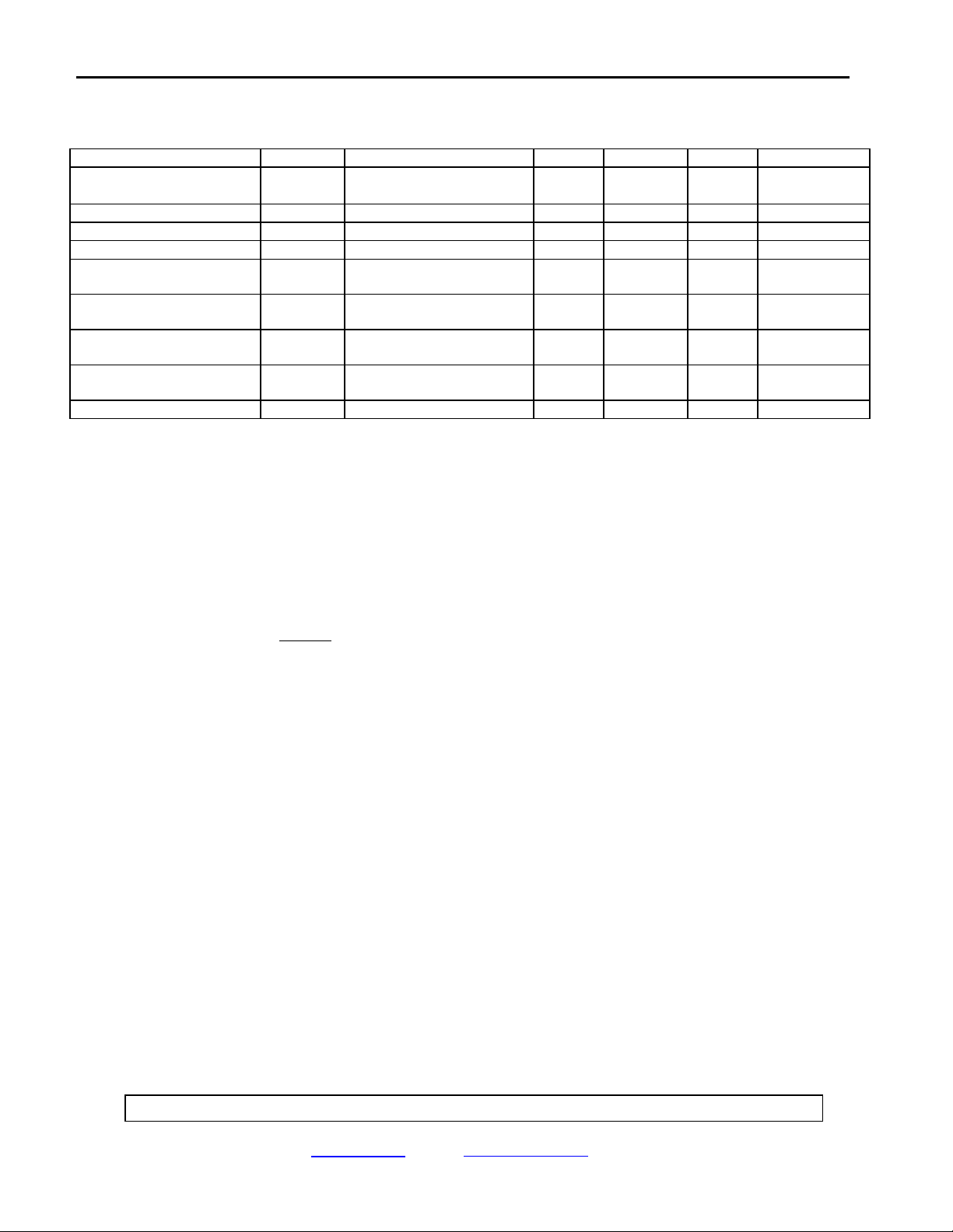
ELECTRICAL CHARACTERISTICS
= 25ºC, V
T
J
= 10 V and I
IN
= -2.0A unless otherwise specified
OUT
PARAMETER SYMBOL TEST CONDITIONS MIN TYP MAX UNIT
Output Voltage (Note 4) V
Line Regulation (Note 2)
Load Regulation (Note 2)
Quiescent Current I
OUT
V
∆
OUT
V
∆
OUT
Q
Ripple Rejection RR I
Output Noise V
Dropout Voltage (Note 5) V
Short-Circuit Current
n
DD
I
OS
I
V
IN
OUT
= V
= 2.0A,
+ 3.5V
OUT
5.0 24 V
VIN = 7.5 to 25V 0.2% 1% V
10mA ≤ I
I
OUT
OUT
f = 210Hz, 5.0V
10Hz ≤ f ≤ 100 kHz
= V
V
IN
I
OUT
I
OUT
VIN = 15V, V
5.0A 0.2% 1% V
≤
OUT
= 0 3.4 10 mA
= 1.0A,
pk-pk
60 dB
50
+ 5.0V
OUT
= 5.0A
= 3.0A
OUT
2.3
2.0
= 5V 7.0 12.0 A
2.5
2.3
V
µ
RMS
V
V
Limit
Control Pin Voltage V
C
4.85 5.0 5.25 V
NOTES:
1. This voltage regulator offers output transistor safe-area protection. However, to maintain full protection, the
device must be operated within the maximum input-to-output voltage differential rating listed on the data sheet
under “Absolute Maximum Ratings”. For applications violating these limits, device will not be fully protected.
2. Load and line regulation are specified at constant junction temperature. Pulse testing is required with a pulse
width ≤ 1 ms and a duty cycle ≤ 5%. Full Kelvin connection methods must be used to measure these parameters.
3. The performance characteristics of the adjustable series (78HGA) is specified for V
= 5.0 V, unless otherwise
OUT
noted.
4. V
is defined as V
OUT
= R1+ R2 (V
OUT
) where R1 and R2 are defined in the Basic Test Circuit diagram.
CONT
R2
5. Dropout Voltage is the input-output voltage differential that causes the output voltage to decrease by 5% of its
initial value.
Micropac Industries cannot assume any responsibility for any circuits shown or represent that they are free from patent infringement.
Micropac reserves the right to make changes at any time in order to improve design and to supply the best product possible.
MICROPAC INDUSTRIES, INC. HYBRID MICROELECTRONICS PRODUCTS DIVISION • 905 E. Walnut St., Garland, TX 75040 • (972) 272-3571 • Fax (972) 494-2281
www.micropac.com E-MAIL: hybridsales@micropac.com
12/13/01
2
Page 3

52150/52175
POSITIVE ADJUSTABLE 5-AMP VOLTAGE REGULATOR
DESIGN CONSIDERATIONS
This device has thermal overload protection from excessive power and internal short circuit protection which limits the
circuit’s maximum current. Thus, the device is protected from overload abnormalities. Although the internal power
dissipation is limited, the junction temperature must be kept below the maximum specified temperature (150ºC). It is
recommended by the manufacturer that the maximum junction temperature be kept as low as possible for increased
reliability. To calculate the maximum junction temperature or heat sink required, the following thermal resistance
values should be used.
Package Type Max
P
θ
JC
TO-3 1.8 2.5
Where: T
T
= Junction Temperature
J
= Ambient Temperature
A
= T
D(MAX)
θ
JC
Solving for T
= Case-to-ambient thermal resistance
θ
CA
– TA
J(max)
+
θ
θ
JC
= TA + PD (
J
CA
=
θ
CA
+
θ
JC
+
θ
θ
CS
SA
)
θ
CA
= Power Dissipation
P
D
θ
= Case-to-heat sink thermal resistance
θ
CS
= Junction-to-case thermal resistance
JC
= Heat sink-to-ambient thermal resistance
θ
SA
The device is designed to operate without external compensation components. However, the amount of external
filtering of these voltage regulators depends upon the circuit layout. If in a specific application the regulator is more
than four inches from the filter capacitor, a 2µF solid tantalum capacitor should be used at the input. A 1µF capacitor
should be used at the output to reduce transients created by fast switching loads, as seen in the basic test circuit.
These filter capacitors must be located as close to the regulator as possible.
Caution: Permanent damage can result from forcing the output voltage higher than the input voltage. A protection
diode from output to input should be used if this condition exists.
VOLTAGE OUTPUT
The device has an adjustable output voltage from 5.0V to 24V which can be programmed by the external resistor
network (potentiometer or two fixed resistors) using the relationship:
Example: If R1 = 0Ω and R2 = 5kΩ, Then
= V
V
OUT
CONTROL
x R1 + R2 V
= 5V nominal.
OUT
R2 Or, if R1 = 10 kΩ and R2 = 5 kΩ then
V
OUT
= 15V
Micropac Industries cannot assume any responsibility for any circuits shown or represent that they are free from patent infringement.
Micropac reserves the right to make changes at any time in order to improve design and to supply the best product possible.
MICROPAC INDUSTRIES, INC. HYBRID MICROELECTRONICS PRODUCTS DIVISION • 905 E. Walnut St., Garland, TX 75040 • (972) 272-3571 • Fax (972) 494-2281
www.micropac.com E-MAIL: hybridsales@micropac.com
12/13/01
3
Page 4

52150/52175
POSITIVE ADJUSTABLE 5-AMP VOLTAGE REGULATOR
Mechanical Configuration
1.551 (39.40)
1.531 (38.19)
.770 (19.56)
MAX.
.293 (7.44)
.273 (6.90)
.421 (10.69)
MIN.
.225 (5.71)
.205 (5.21)
1.197 (30.40)
1.177 (29.30)
PIN 1
.041 (1.04)
.037 (0.94)
PIN 2
SEATING PLANE
.067 (1.70)
MAX.
DIA.
.675 (17.14)
.655 (16.64)
Ø.161 (4.09)
Ø.151 (3.84)
2 HOLES
.440 (11.16)
.420 (10.57)
0.47 (11.34)
DIA. PIN CIRCLE
PIN 4
12°
54°
Test Circuit Adjustable Output Voltage
3
V
IN
C =2uF
IN
SOLID
TANTALUM
Note: All dimensions in inches and millimeters (parentheses).
4
2
1
PIN 3
R1
R2
R .177 (4.5)
V
OUT
C >1.0uF
L
Micropac Industries cannot assume any responsibility for any circuits shown or represent that they are free from patent infringement.
Micropac reserves the right to make changes at any time in order to improve design and to supply the best product possible.
MICROPAC INDUSTRIES, INC. HYBRID MICROELECTRONICS PRODUCTS DIVISION • 905 E. Walnut St., Garland, TX 75040 • (972) 272-3571 • Fax (972) 494-2281
www.micropac.com E-MAIL: hybridsales@micropac.com
12/13/01
4
 Loading...