

Page 1
RTD TRANSMITTER
Programmable via PC
Input for Pt100, Ni100 or Ohm
Linearised analogue output
24 VDC supply
1- or 2-channel version
DIN rail mounting
5102
Application:
Linearised temperature measurement with Pt100 or Ni100
sensor. • Conversion of linear resistance change to standard
analogue current / voltage signal from e.g. valves or linear
movements with attached potentiometer. • Signal simulator
via externally mounted 10-turn potentiometer.
Technical characteristics:
General:
The transmitter may be configured to the requested signal
type by means of a DOS-based PC with the configuration
program PReset 5000 and the communi cations unit Loop
Link. The configuration of the transmitter may be done
without connection of supply voltage as the communications
unit supplies the required power. The supply voltage is 24
VDC with the same reference point for supply, input and
output ground. The sensor connection is always a 3-wire
connection with cable compensation for up to 50 Ω in each
wire. If a 2-wire connection is requested, pins 43 and 42
(channel 1) or 53 and 52 (channel 2) must be short-circuited
in the connection plug (no cable compensation). Sensor
error detection is as standard set to Upscale, Downscale or
entered to special output value.
Input:
Linearised Pt100 temperature input according to IEC
751 within the range -200...+850°C. Linearised Ni100
temperature input according to DIN 43760 within the range
-50...+250°C. Linear resistance input within the range 0...10
kΩ. Min. span for the RTD input is 50°C, for linear resistance
30 Ω. The RTD input can be delivered set up in multiples of
the main type (e.g. Pt1000). The input can be reversed so
that 0% e.g. is 150°C and 100% is 0°C.
Output:
The analogue output may be configured to any current
within the range 0...20 mA or voltage within the range 0...10
VDC with a min. span of 5 mA or 250 mVDC with a max.
offset of 50% of the actual max. value. Voltage signals are
produced by short-circuiting pins 13 and 12 (channel 1)
or 23 and 22 (channel 2) together with mounting a jumper
for internal shunt resistance. For voltage signals within the
range 0...1 VDC a 50 Ω shunt (JP1) is used, within the range
0...10 VDC a 500 Ω shunt (JP2) is used. The voltage signal
is available between pins 12 and 11 (channel 1), or 22 and
21 (channel 2). The min. load resistance for voltage signals
is 500 kΩ.
Electrical specifications:
Specifications range:
-20°C to +60°C
Common specifications:
Supply voltage ................................... 19.2...28.8 VDC
Internal consumption ......................... 1.7 W (2 channels)
Warm-up time .................................... < 5 min.
Communications interface ................ Loop Link
Signal / noise ratio ............................. Min. 60 dB
Signal dynamics, input ...................... 17 bit
Signal dynamics, output .................... 16 bit
Response time (0...90%, 100...10%) .. < 165 ms
Calibration temperature ..................... 20...28°C
Temperature coefficient ..................... < ±0.01% /°C
Linearity error .................................... < 0.1% of span
EMC immunity influence ................... < ±0.5% of span
Screw terminal torsion ....................... 0.5 Nm
Humidity ............................................ < 95% RH (non-cond.)
Dimensions (HxWxD) ......................... 109 x 23.5 x 130 mm
DIN rail type ....................................... DIN 46277
Protection degree .............................. IP20
Weight ............................................... 170 g
Input:
Type Min. value Max. value Min. span Standard
Pt100 -200°C +850°C 50°C IEC 751
Ni100 -50°C +250°C 50°C DIN 43760
Lin.R 0 Ω 10 kΩ 30 Ω -----
Max. offset ......................................... 50% of selected max. value
Cable resistance per wire (prog.). ...... Max. 10...50 Ω
Sensor current ................................... > 0.2, < 0.4 mA
Basic accuracy .................................. < ±0.3°C
Temp. coefficient for span <100°C .... < ±0.01°C/°C
Sensor error detection ....................... Upscale/Downscale/selec. value
Output:
Signal range ...................................... 0...20 mA / 0...10 VDC
Min. signal range ............................... 5 mA / 250 mV
Max. offset ......................................... 50% of selected max. value
Load (max.) ........................................ 20 mA / 600 Ω / 12 VDC
Load stability ..................................... < 0.01% of span / 100 Ω
Current limit ....................................... < 28 mA
GOST R approval:
VNIIM, Cert. no. ................................... See www.prelectronics.com
Observed authority requirements: Standard:
EMC 2004/108/EC ............................ EN 61326-1
Of span = Of the presently selected range
amb.
amb.
Lerbakken 10 · DK-8410 Rønde
Tlf. 8637 2677 · Fax 8637 3085
www.prelectronics.dk
Page 2
Order: 5102
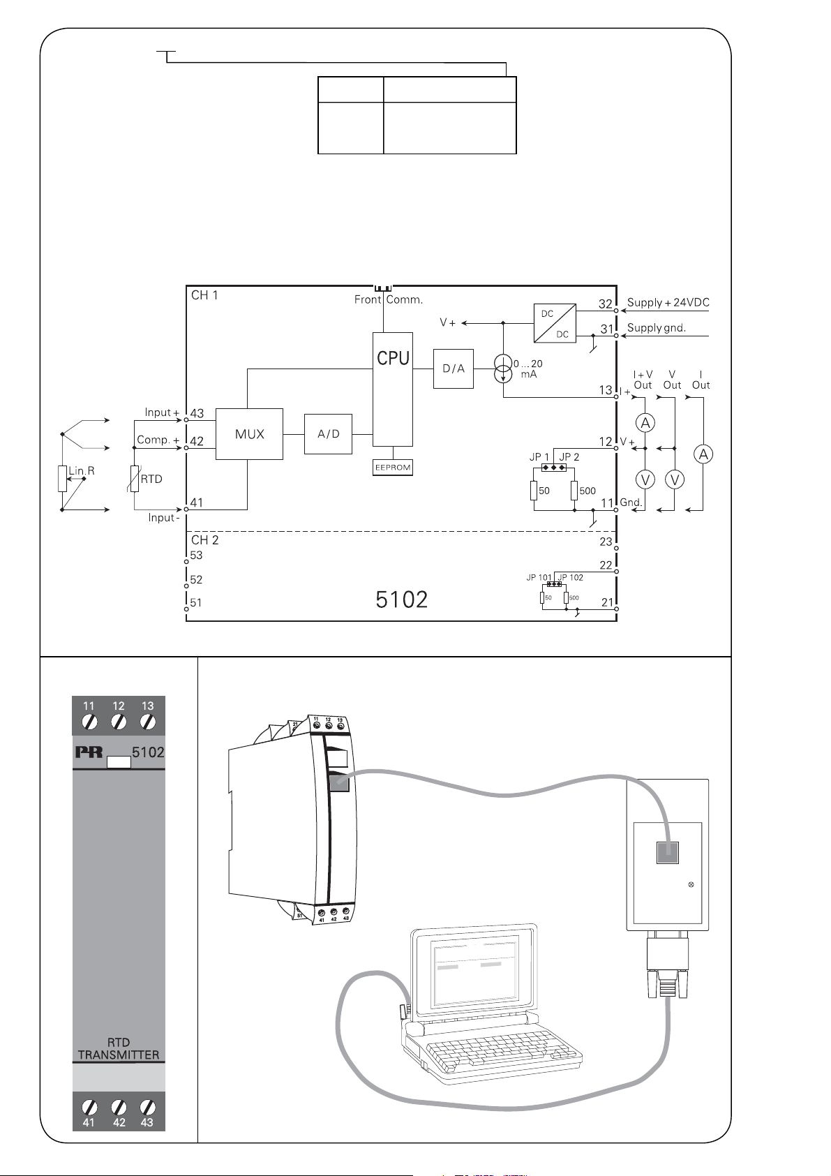
Block diagram:
Type
Channels
5102 1 channel : A
2 channels : B
For 2-wire connection, short-circuit pins 42 and 43.
Front layout: 5102 connection to Loop Link:
CH 2
CH 1
5102
NB: The module can be programmed
whether the supply is connected or disconnected. If the supply is connected during
programming, the module must be disconnected and then reconnected after programming.
0
0
:
0
:
3
8
0
n
i
o
t
p
O
e
g
a
u
g
a
n
L
n
i
o
t
a
i
c
n
u
m
m
o
C
t
u
p
t
u
O
t
u
p
n
I
t
c
u
d
r
o
P
l
e
i
F
D
e
S
a
T
n
I
I
n
C
C
R
3
1
3
5
p
o
t
e
R
P
0
1
-
8
-
4
9
1
9
:
e
t
a
4
9
1
5
0
2
3
4
9
:
o
l
n
a
r
i
s
c
i
n
r
o
t
c
l
e
e
R
P
:
o
n
g
t
u
p
n
i
g
l
o
a
n
A
:
e
p
y
t
u
t
p
:
e
n
g
a
r
t
u
p
:
n
i
o
t
c
n
e
n
o
m
o
c
n
i
o
t
c
n
j
u
d
o
l
:
e
m
t
i
s
e
n
o
p
s
e
t
u
t
p
u
o
g
o
l
a
n
A
A
0
m
2
-
4
:
e
p
y
t
t
u
p
t
u
O
C
E
I
/
N
I
D
0
0
1
t
P
0
0
.
0
i
w
-
3
-
-
-
-
-
-
:
p
0
0
.
1
e
l
a
c
s
p
U
:
r
r
o
r
e
r
o
s
e
n
S
C
0
0
.
5
0
r
e
c
e
s
COM
Loop Link
5102Y103-UK (0910)
 Loading...