

Page 1

RADIATION TOLERANT, ± 90V - 0.8A
53124
POWER MOSFET OPTOCOUPLER
Mii
HYBRID MICROELECTRONICS
PRODUCTS DIVISION
Features:
• Design Tested to 100 krad (Si) Total Dose
• Hermetically Sealed in 8-Pin Dual-In-Line
Package
• Performance over –55°C to +125°C
• Compact Solid State Bi-directional Switch
• AC/DC Power Switching
• Maximum Average Current
AC/DC: 0.8 A
DC only: 1.6 A
(1)
(1)
Per Derating Curves (Figure 3)
AC/DC: 0.5 A
DC only: 1.0 A
• Optically Coupled
• Input/Output Isolation Tested to 1500 VDC
• High Level of Transient Immunity
• 3 A Output Surge Current
• Shock and Vibration Resistant
• MIL-PRF-38534
• Same foot print as HSSR7111 / Mii 53111 &
Electrically Similar
DESCRIPTION
Applications:
• Satellite/Space systems
• Military/High Reliability Systems
• Standard 28 VDC and 48 VDC Load Driver
• Standard 24 VAC Load Driver
• Aircraft Controls
• AC/DC Electromechanical and Solid State
Relay Replacement
• I/O Modules
• Switching Heaters
The 53124 is a single channel power MOSFET optocoupler which is suitable as a pin for pin replacement for the Mii
53111 when radiation tolerant performance and similar electrical performance to the 53111 is required. The primary
difference between the 53124 and 53111 is that the radiation tolerant power MOSFETs employed in the 53124
exhibit a higher R
The higher values of R
DS(ON).
results in a lower current for the same power dissipation or
DS(ON)
higher power dissipation for the same current levels relative to the 53111.
The popular eight pin, hermetic dual-in-line ceramic package combined with 1500 VDC isolation between input and
output, makes this optocoupler ideal for solid-state relay applications. Performance is specified over the full military
temperature range. This device is available as COTS, or as fully compliant MIL-PRF-38534 Class H or with custom
screening. Lead options support both through-hole and surface-mount assembly. Gold plated leads are standard,
but other lead finishes per MIL-PRF-38534 are also available.
Functionally, the device operates as a single-pole, normally open (1 Form A) solid-state relay. The device is
actuated by an input current, which can be supplied from standard logic types such as open-collector TTL. The
input current biases a light emitting diode that is optically coupled to an integrated photovoltaic diode array. The
photovoltaic array powers control circuitry that operates the output MOSFETs. Optimum switching of either AC or
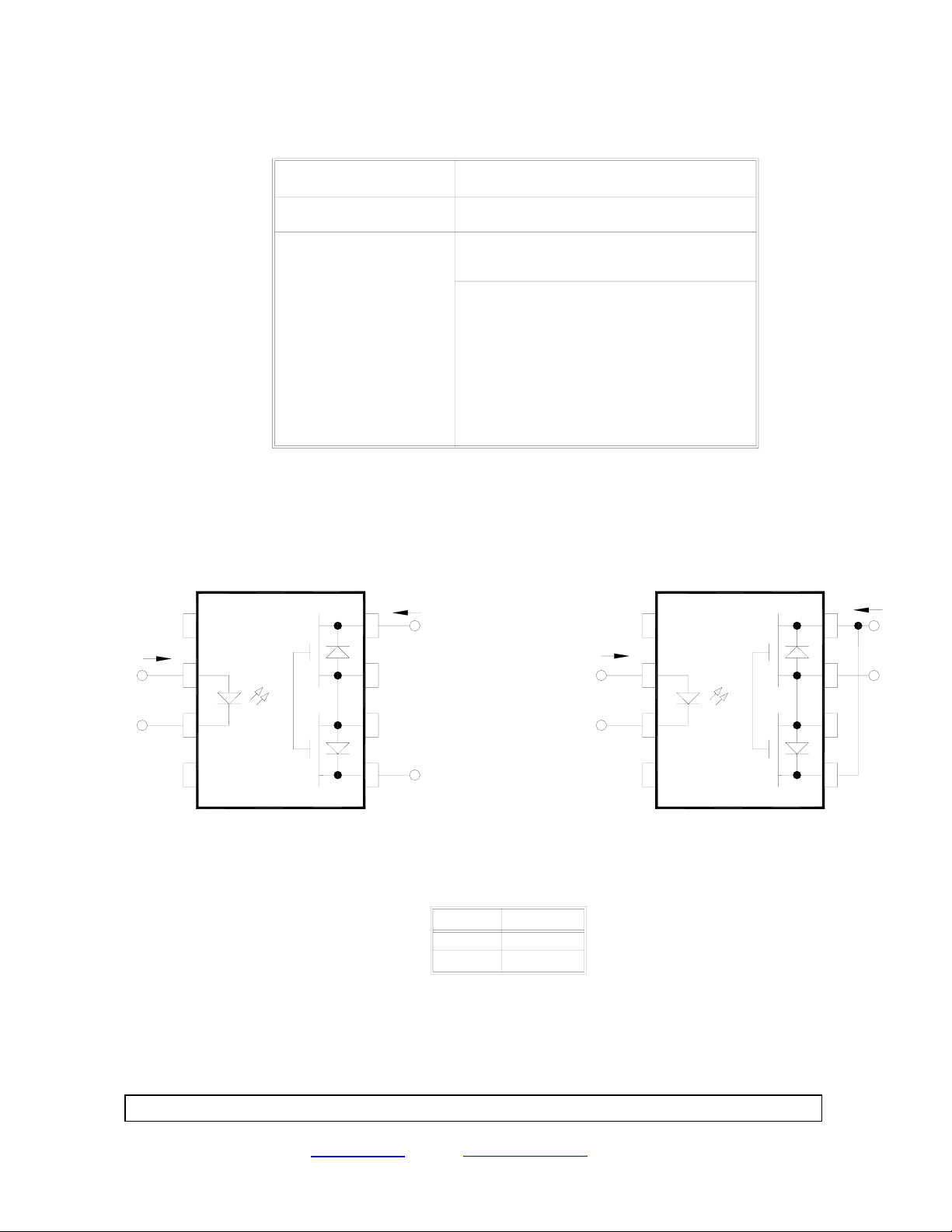
DC loads is provided by a configurable output. For AC loads, Connection A in Figure 1 must be used. Connection
A will also switch DC loads but Connection B, in Figure 1, provides DC-only operation with the advantages of
substantial reduction in on-resistance and twice the output current capability as that obtained with Connection A.
Micropac Industries cannot assume any responsibility for any circuits shown or represent that the y are free from patent infringement.
Micropac reserves the right to make changes at any time in order to improve design and to suppl y the best product possible.
MICROPAC INDUSTRIES, INC. HYBRID MICROELECTRONICS PRODUCTS DIVISION • 905 E. Walnut St., Garland, TX 75040 • (972) 272-3571 • Fax (972) 494-2281
www.micropac.com
E-MAIL: [email protected] 02/15/01
Page 2

53124
Radiation Tolerant Power MOSFET Optocoupler
___________________________________________________________________________________________
ABSOLUTE MAXIMUM RATINGS:
Storage Temperature Range ..……………………………………………………….........……............... -65°C to +150°C
Operating Ambient Temperature - T
Junction Temperature - T
..............................……………………………………………...…….......….........…. +150°C
J
Operating Case Temperature - T
...................…………………………………………..….…..….. -55°C to +125°C
A
.....................………………………………………...……….……............ +145°C
c
Lead Solder Temperature for 10 seconds .......................………………………………………....…….............. +260°C
(1.6 mm below seating plane)
Average Input Current - I
Peak Repetitive Input Current - I
....................…...……………………………………………..……..........…............... 20 mA
F
.............…………………………………...…………………........…............. 40 mA
Fpk
(Pulse width < 100 ms; duty cycle < 50%)
Peak Surge Input Current - I
surge .............……………………………………………………….................. 100 mA
Fpk
(Pulse width < 0.2 ms; duty cycle < 0.1%)
Reverse Input Voltage - V
................................…………………………..……………………………..................... 5 V
R
Average Output Current
Connection A - I
Connection B - I
........................…………………………..…………………..……….................................... 0.8 A
O
..............................................………..………………………..……………………............ 1.6 A
O
Average Output Current, derated per Figure 3
Connection A - I
Connection B - I
.......................................…………………………………………..……………..................... 0.5 A
O
........................................……………………………………………………..….................... 1.0 A
O
Single Shot Output Current - Figure 4
Connection A - I
Connection B - I
surge (Pulse width < 10 ms) ........………………………………………..…...…………...... 3 A
Opk
surge (Pulse width < 10 ms) .........………………………………………..………………..... 6 A
Opk
Output Voltage
Connection A - V
Connection B - V
Average Output Power Dissipation - Figure 5 ........………………………………………….…………….... 800 mW
.........................……………………………………………………..……..…......... –90 V to +90 V
O
............................…...……………………………………………………….............. 0 V to +90 V
O
(3)
(2)
(1)
(1)
RECOMMENDED OPERATING CONDITIONS:
Parameter Symbol Min. Max. Units
Input Current (ON) I
Input Voltage (OFF) V
Operating
Temperature
Micropac Industries cannot assume any responsibility for any circuits shown or represent that the y are free from patent infringement.
Micropac reserves the right to make changes at any time in order to improve design and to suppl y the best product possible.
MICROPAC INDUSTRIES, INC. HYBRID MICROELECTRONICS PRODUCTS DIVISION • 905 E. Walnut St., Garland, TX 75040 • (972) 272-3571 • Fax (972) 494-2281
www.micropac.com
F (ON)
F (OFF)
T
A
E-MAIL: [email protected] 02/15/01
520mA
00.6VDC
-55 +125 °C
Page 3
53124
Radiation Tolerant Power MOSFET Optocoupler
___________________________________________________________________________________________
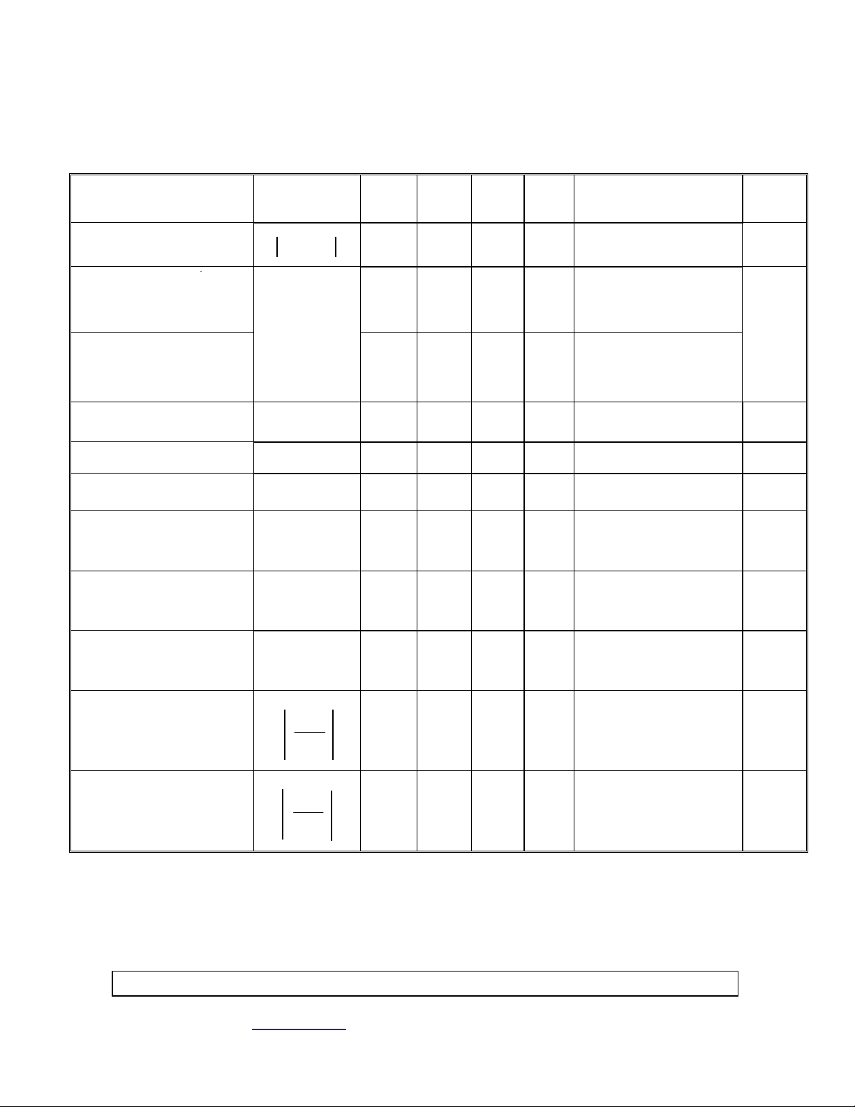
ELECTRICAL SPECIFICATIONS (Pre-Irradiation)
= -55°C to +125°C, unless otherwise specified.
T
A
Parameter Symbol Min. Typ.* Max. Unit
Output Withstand Voltage V
O(OFF)
Output On-Resistance
(Connection A)
R
Output On-Resistance
(Connection B)
Output Leakage Current I
O (OFF)
Input Forward Voltage V
Input Reverse Breakdown
Voltage
Input-Output Insulation I
Turn-On Time t
Turn-Off time t
Output Transient Rejection
Input-Output Transient
dV
dV
Rejection
(ON)
V
I-O
ON
OFF
dt
dt
F
R
I-O
Test Conditions Notes
s
= 0.6 V
V
90 110 V
0.8 2.5
Ω
F
= 10 µA
I
O
I
= 10 mA
F
= 500 mA
I
O
(pulse duration ≤ 30 ms)
4,
Figure
I
= 10 mA
0.2 0.7
F
I
Ω
= 1 A
O
1
(pulse duration ≤ 30 ms)
= 0.6 V
V
10
-4
10
µA
F
V
= 90 V
O
1.0 1.24 1.7 V IF = 10 mA
5V
I
= 10 µA
F
RH ≤ 45%, t = 5 s
1
1.25 6 ms
0.25 ms
O
1000
500
µA
V/µs
V/µs
V
= 1500 VDC
I-O
T
= 25°C
A
= 10 mA
I
F
V
= 28 V
DD
I
= 800 mA
O
= 10 mA
I
F
= 28 V
V
DD
I
= 800 mA
O
V
= 50 V
PEAK
C
= 1000 pF
M
C
= 15 pF
L
≥ 1 MΩ
R
M
V
= 5 V
DD
V
I-O (PEAK)
= 20 kΩ
R
L
C
= 15 pF
L
= 50 V
5, 6
Figure
6
Figure
6
Figure
7
Figure
8
* All typical values are at TA = 25°C, I
Micropac Industries cannot assume any responsibility for any circuits shown or represent that the y are free from patent infringement.
Micropac reserves the right to make changes at any time in order to improve design and to suppl y the best product possible.
MICROPAC INDUSTRIES, INC. HYBRID MICROELECTRONICS PRODUCTS DIVISION • 905 E. Walnut St., Garland, TX 75040 • (972) 272-3571 • Fax (972) 494-2281
www.micropac.com
F (ON)
= 10 mA, V
E-MAIL: [email protected] 02/15/01
= 0.6 V unless otherwise specified.
F (OFF)
Page 4

53124
Radiation Tolerant Power MOSFET Optocoupler
___________________________________________________________________________________________
TYPICAL CHARACTERISTICS - (Pre-Irradiation)
All typical values are at T
= 25°C, I
A
= 10 mA, V
F (ON)
= 0.6 V unless otherwise specified.
F (OFF)
Parameter Symbol Test Conditions Typical Value Units Notes
Output Off-Capacitance C
O (OFF)
Output Offset Voltage V
Input Diode Temperature Coefficient
∆V
Input Capacitance C
Input-Output Capacitance C
Input-Output Resistance R
F
OS
/∆T
IN
I-O
I-O
VO = 28 V
f = 1 MHz
IF = 10 mA
= 0 mA
I
O
A
IF = 10 mA -1.4 mV/°C
VF = 0 V
f = 1 MHz
V
= 0 V
I-O
f = 1 MHz
V
= 500 V
I-O
t = 60 s
145 pF
2
20 pF 8
1.5 pF 5
13
10
Notes:
1. Maximum average current rating where the case temperature (T
) is maintained below 120°C.
C
2. Maximum junction to case thermal resistance for the device is 15°C/W, where case temperature (T
measured at the center of the package bottom.
3. For rating, see Figure 5. The output power P
average output current I
4. During the pulsed R
as shown in Figure 3.
O
measurement (IO duration < 30 ms), ambient (TA) and case temperature (TC) are equal.
ON
rating curve is obtained when the part is handling the maximum
D
5. Pins 2 through 3 shorted together and pins 5 through 8 shorted together.
6. This is a momentary withstand test, not an operating condition.
7. V
is a function of IF and is defined between pins 5 and 8, with pin 5 as the reference. VOS must be measured
OS
in a stable ambient (free of temperature gradients).
8. Zero-bias capacitance measured between the LED anode and cathode.
µV
Ω
C
7
5
) is
CAUTION:
Care should be taken not to exceed the maximum output power dissipation, maximum case temperature, and
maximum junction temperature when repetitively switching loads.
Micropac Industries cannot assume any responsibility for any circuits shown or represent that they are free from patent infringement.
Micropac reserves the right to make changes at any time in order to improve design and to supply the best product possible.
MICROPAC INDUSTRIES, INC. HYBRID MICROELECTRONICS PRODUCTS DIVISION • 905 E. Walnut St., Garland, TX 75040 • (972) 272-3571 • Fax (972) 494-2281
www.micropac.com E-MAIL: [email protected]
02/15/01
Page 5
53124
Radiation Tolerant Power MOSFET Optocoupler
___________________________________________________________________________________________
Case outlines A, B, and C
Terminal number Terminal symbol
Connection A Conneciton B
(AC or DC load) (DC load only)
1
2
3
4
5
6
7
8
NC
V
V
NC
V
NC
NC
V
F+
F-
O-
O+
NC
V
V
NC
V
NC
N
V
F+
F-
O+
OO+
NC = No connection
CONNECTION A
AC/DC CONNECTION
I
O
1
I
F
2
+
V
F
3
-
8
+
7
V
O
6
I
F
+
V
F
-
CONNECTION B
DC CONNECTION
1
2
3
I
O
8
7
+
V
O
-
6
4
-
545
Figure 1 - Terminal Connections
INPUT OUTPUT
OFF OFF
ON ON
Figure 2 - Truth Table
Micropac Industries cannot assume any responsibility for any circuits shown or represent that they are free from patent infringement.
Micropac reserves the right to make changes at any time in order to improve design and to supply the best product possible.
MICROPAC INDUSTRIES, INC. HYBRID MICROELECTRONICS PRODUCTS DIVISION • 905 E. Walnut St., Garland, TX 75040 • (972) 272-3571 • Fax (972) 494-2281
www.micropac.com E-MAIL: [email protected]
02/15/01
Page 6
53124
Radiation Tolerant Power MOSFET Optocoupler
___________________________________________________________________________________________
0.6
0.5
0.4
0.3
0.2
CONNECTION - A
≥
10 mA
I
0.1
F
__
θ
= 40°C/W
O
I - OUTPUT CURRENT- A
0
CA
-
-
θ
= 80°C/W
CA
65
-25-55
T - AMBIENT TEMPERATURE - °C
A
35-5
12595 155
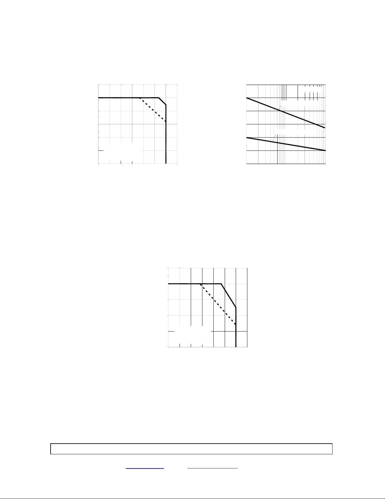
Figure 3. Maximum Average Output
Current Rating vs. Ambient
Temperature.
OPK
I - SURGE - OUTPUT CURRENT - A
7
6
CONNECTION - B
5
4
CONNECTION - A
3
2
1
10
PULSE DURATION - ms
100
I
F
≥
10 mA
Figure 4. Single Shot (nonrepetitive) Output Current vs. Pulse
Duration.
1000
1.0
0.8
0.6
0.4
CONNECTION - A
0.2
DISSIPATION - W
D
P - OUTPUT POWER
≥
10 mA
I
F
__
θ
= 40°C/W
CA
-
-
θ
= 80°C/W
0
-55 -25
CA
655 35 95 125 155
T - AMBIENT TEMPERATURE - °C
A
Figure 5. Output Power Rating vs.
Ambient Temperature.
Micropac Industries cannot assume any responsibility for any circuits shown or represent that they are free from patent infringement.
Micropac reserves the right to make changes at any time in order to improve design and to supply the best product possible.
MICROPAC INDUSTRIES, INC. HYBRID MICROELECTRONICS PRODUCTS DIVISION • 905 E. Walnut St., Garland, TX 75040 • (972) 272-3571 • Fax (972) 494-2281
www.micropac.com E-MAIL: [email protected]
02/15/01
Page 7
53124
Radiation Tolerant Power MOSFET Optocoupler
___________________________________________________________________________________________
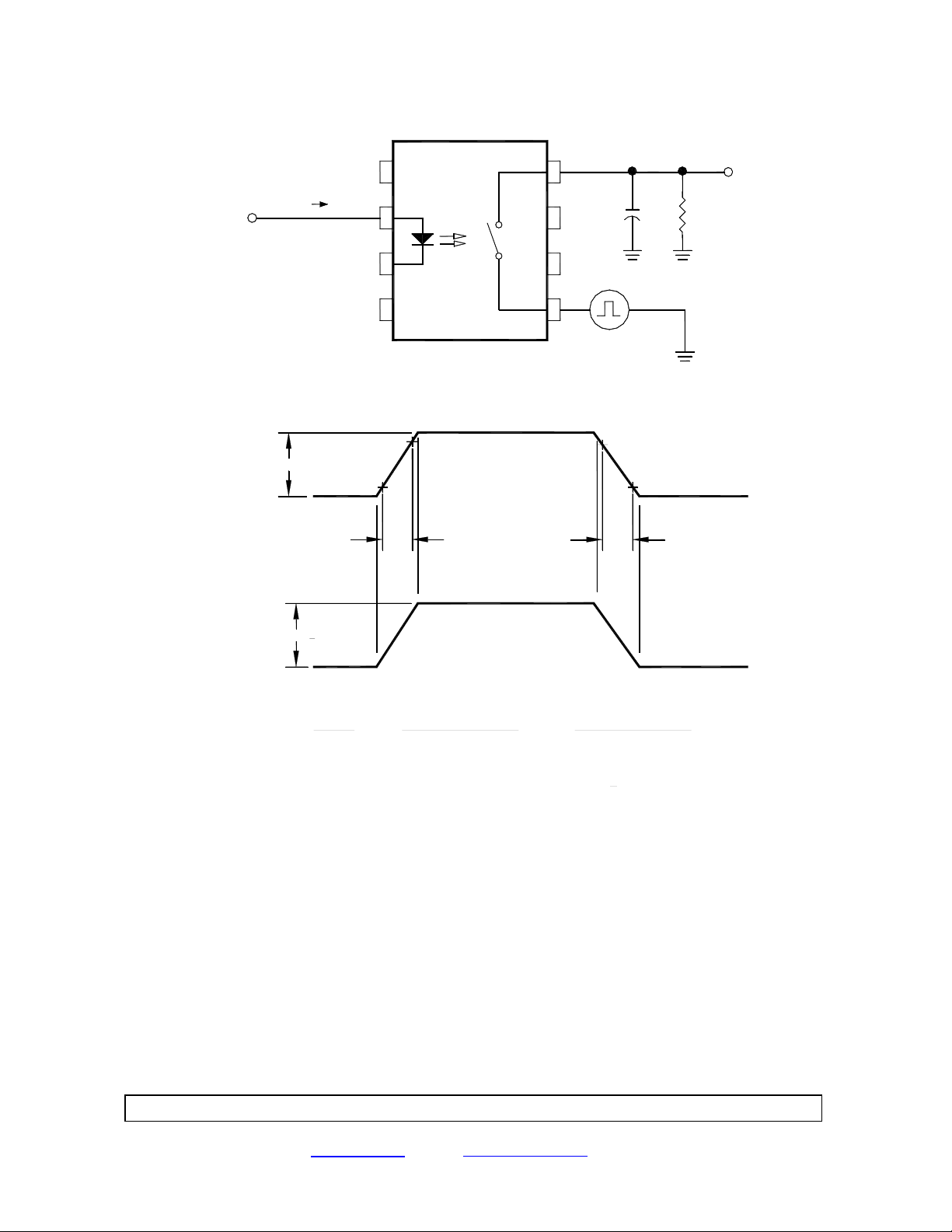
PULSE GEN
(SEE NOTE 1)
I
F
MONITOR
GND
I
R
200
50%
V
DD
R
L
V
O
1
8
MONITOR
NODE
F
2
+
V
F
-
3
4
7
6
5
C
= 25 pF
L
(SEE NOTE 2)
M
GND
50%
I
F
PULSE
WIDTH
V
O
= 15 ms
90%
10%
t
ON
NOTES:
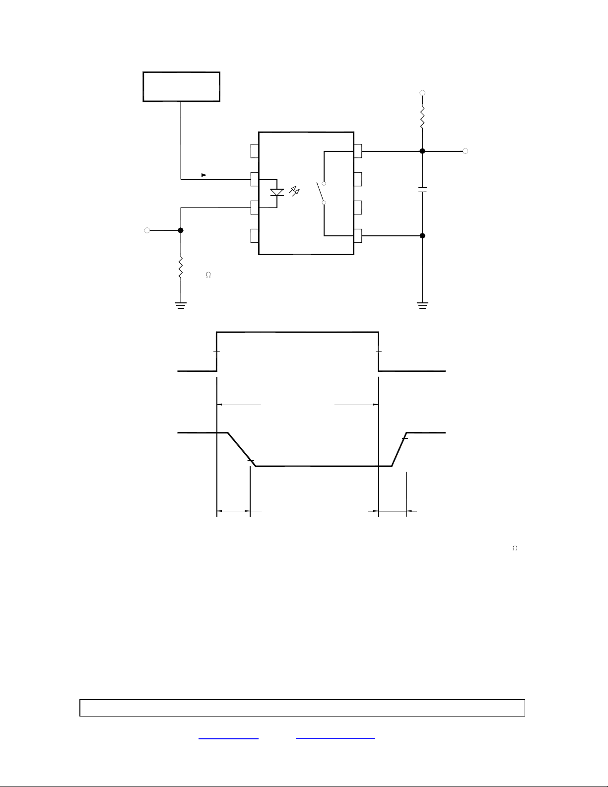
1. PULSE GENERATOR HAS THE FOLLOWING CHARACTERISTICS: OUTPUT IMPEDANCE = 50
AND t
= t = 5.0 ns.
2. LOAD CAPACITANCE (C
r f
) INCLUDES PROBE AND JIG CAPACITANCE.
L
t
OFF
Figure 6. Switching Test Circuit and Waveform.
Micropac Industries cannot assume any responsibility for any circuits shown or represent that they are free from patent infringement.
Micropac reserves the right to make changes at any time in order to improve design and to supply the best product possible.
MICROPAC INDUSTRIES, INC. HYBRID MICROELECTRONICS PRODUCTS DIVISION • 905 E. Walnut St., Garland, TX 75040 • (972) 272-3571 • Fax (972) 494-2281
www.micropac.com E-MAIL: [email protected]
02/15/01
Page 8
53124
Radiation Tolerant Power MOSFET Optocoupler
___________________________________________________________________________________________
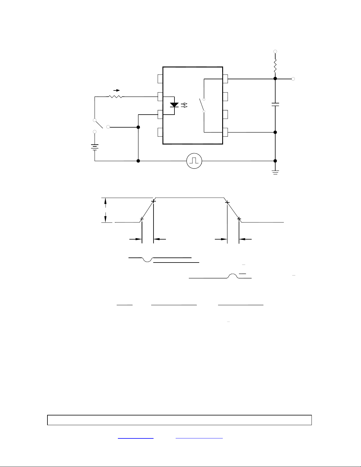
V
M
INPUT
OPEN
1
I
F
2
+
V
F
-
3
4
8
7
6
5
V
O(PEAK)
+
C
M
R
-
PULSE
GENERATOR
MONITOR
NODE
M
90%
V
O(PEAK)
10%
t
r
V (MAX) < 5V
M
V
d
O
d
t
OVERSHOOT ON V
(0.8) V
=
O (PEAK)
t
r
OR
O (PEAK) IS TO BE < 10%
NOTES:
1. C INCLUDES PROBE AND FIXTURE CAPACITANCE.
M
2. R
INCLUDES PROBE AND FIXTURE RESISTANCE.
M
t
(0.8) V
90%
10%
f
O (PEAK)
t
f
Figure 7. Output Transient Rejection Test Circuit and Waveform.
Micropac Industries cannot assume any responsibility for any circuits shown or represent that they are free from patent infringement.
Micropac reserves the right to make changes at any time in order to improve design and to supply the best product possible.
MICROPAC INDUSTRIES, INC. HYBRID MICROELECTRONICS PRODUCTS DIVISION • 905 E. Walnut St., Garland, TX 75040 • (972) 272-3571 • Fax (972) 494-2281
www.micropac.com E-MAIL: [email protected]
02/15/01
Page 9
53124
Radiation Tolerant Power MOSFET Optocoupler
___________________________________________________________________________________________
V
DD
R
L
S1
V
B
IN
V
I-0 (PEAK)
1
I
F
+
V
F
-
3
A
4
V
I-0 (PEAK)
+
-
8
72
6
5
V
O
C
L
PULSE
GENERATOR
t
90%
10%
f
10%
90%
t
r
V
O (OFF)
S
AT A (V = 0 V)
1
F
dV
I-0
d
=
t
OVERSHOOT ON VOVERSHOOT ON V
V
O (ON)
AT B (I = 10 mA)
S
1
(0.8) V
I-0 (PEAK)
t
r
I-0 (PEAK) IS TO BE < 10 %
F
V
O (OFF)
OR
(MIN) > 3.25 V
(0.8) V
I-0 (PEAK)
t
f
V
O (ON)
(MAX) < 0.8 V
NOTES:
1. LOAD CAPACITANCE (C
Micropac Industries cannot assume any responsibility for any circuits shown or represent that they are free from patent infringement.
Micropac reserves the right to make changes at any time in order to improve design and to supply the best product possible.
)INCLUDES PROBE AND FIXTURE CAPACITANCE.
L
MICROPAC INDUSTRIES, INC. HYBRID MICROELECTRONICS PRODUCTS DIVISION • 905 E. Walnut St., Garland, TX 75040 • (972) 272-3571 • Fax (972) 494-2281
www.micropac.com E-MAIL: [email protected]
02/15/01
Page 10
53124
Radiation Tolerant Power MOSFET Optocoupler
___________________________________________________________________________________________
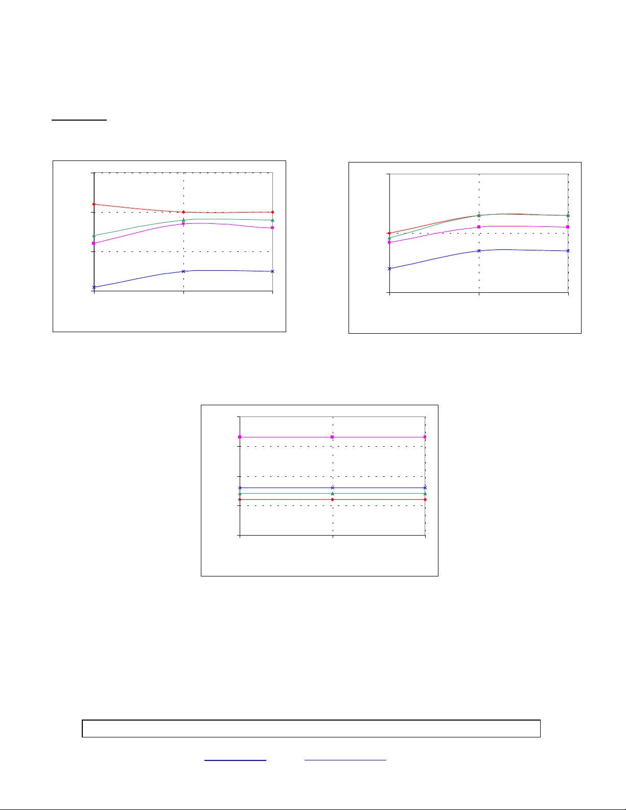
TOTAL DOSE TEST RESULTS
Disclaimer: The data of 4 representative units irradiated in Cobalt-60 chamber is only typical of one lot of
solid state relays. Micropac does not guarantee performance of its SSR to these radiation levels. Individual
lots have to be screened to guarantee the performance.
3.0
1.5
2.5
1.0
2.0
Turn-On Time, ms
1.5
050100
Total Dose, krad (Si)
Rise Time, ms
0.5
050100
Total Dose, krad (Si)
Figure 9. Turn-On Time vs Total Dose Figure 10. Rise Time vs Total Dose
at V
I
= 28 V, R
out
= 15 mA, 10% duty cycle. Iin = 15 mA, 10% duty cycle.
in
= 35 Ω, at V
load
= 28 V, R
out
= 35 Ω,
load
90
s
80
µ
70
60
Turn-Off Time,
50
0 50 100
Total Dose, krad (Si)
Figure 11. Turn-Off Time vs Total Dose at V
R
Micropac Industries cannot assume any responsibility for any circuits shown or represent that they are free from patent infringement.
Micropac reserves the right to make changes at any time in order to improve design and to supply the best product possible.
MICROPAC INDUSTRIES, INC. HYBRID MICROELECTRONICS PRODUCTS DIVISION • 905 E. Walnut St., Garland, TX 75040 • (972) 272-3571 • Fax (972) 494-2281
www.micropac.com E-MAIL: [email protected]
= 35 Ω, Iin = 15 mA, 10% duty cycle.
load
= 28 V,
out
02/15/01
Page 11
53124
Radiation Tolerant Power MOSFET Optocoupler
___________________________________________________________________________________________
0.80
0.75
On-Resistance "A", ohm
0.70
050100
Total Dose, krad (Si)
0.20
0.19
On-Resistance "B", ohm
0.18
050100
Total Dose, krad (Si)
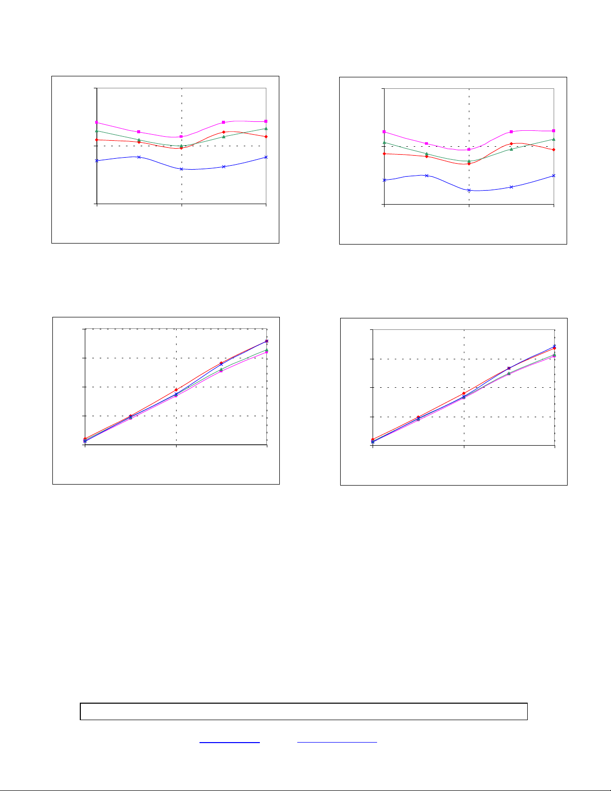
Figure 12. On-Resistance "A" vs Total Dose Figure 13. On-Resistance "B" vs Total Dose
at I
4
3
=10 mA, I
F
= 40 mA for 1second. at IF =10 mA, I
out
8
6
= 40 mA for 1second.
out
2
1
Output Leakage Current "A", nA
0
050100
Total Dose, krad (Si)
4
2
Output Leakage Current "B", nA
0
050100
Total Dose, krad (Si)
Figure 14. Output Leakage Current "A" vs Total Dose Figure 15. Output Leakage Current "B" vs Total
at V
= 1.0 V, V
F
= 90 V. Dose at VF = 1.0 V, V
out
= 90 V.
out
Micropac Industries cannot assume any responsibility for any circuits shown or represent that they are free from patent infringement.
Micropac reserves the right to make changes at any time in order to improve design and to supply the best product possible.
MICROPAC INDUSTRIES, INC. HYBRID MICROELECTRONICS PRODUCTS DIVISION • 905 E. Walnut St., Garland, TX 75040 • (972) 272-3571 • Fax (972) 494-2281
www.micropac.com E-MAIL: [email protected]
02/15/01
Page 12
53124
Radiation Tolerant Power MOSFET Optocoupler
___________________________________________________________________________________________
1.40
60
40
1.35
20
Input Forward Voltage, VDC
1.30
050100
Total Dose, krad (Si)
Input Reverse Voltage, VDC
0
050100
Total Dose, krad (Si)
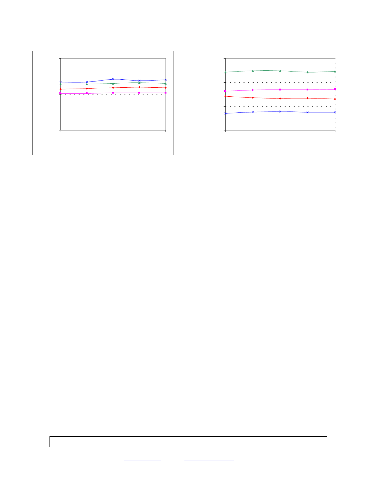
Figure 16. Input Forward Voltage vs Total Dose Figure 17. Input Reverse Voltage vs Total Dose
at I
=15 mA. at IR = 10 µA.
F
Micropac Industries cannot assume any responsibility for any circuits shown or represent that they are free from patent infringement.
Micropac reserves the right to make changes at any time in order to improve design and to supply the best product possible.
MICROPAC INDUSTRIES, INC. HYBRID MICROELECTRONICS PRODUCTS DIVISION • 905 E. Walnut St., Garland, TX 75040 • (972) 272-3571 • Fax (972) 494-2281
www.micropac.com E-MAIL: [email protected]
02/15/01
Page 13
53124
Radiation Tolerant Power MOSFET Optocoupler
___________________________________________________________________________________________
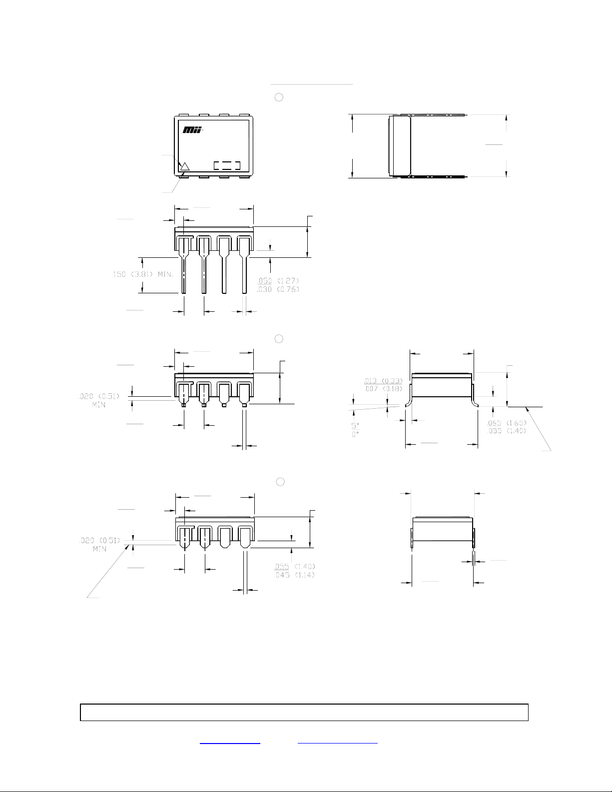
Case Outlines
A
-101 CASE OUTLINE
31757 USA
.310 (7.87)
.290 (7.37)
ESD
SYMBOL
PIN 1
.050 (1.27)
.035 (0.89)
53124
XXXXX
Q
.390 (9.91)
.370 (9.41)
.320 (8.13)
MAX.
.170 (4.32)
MAX.
.110 (2.79)
.090 (2.29)
.050 (1.27)
.035 (0.89)
.110 (2.79)
.090 (2.29)
.050 (1.27)
.035 (0.89)
.110 (2.79)
.090 (2.29)
SEATING PLANE
.020 (0.51)
MAX.
B
.390 (9.91)
.370 (9.41)
-102 CASE OUTLINE
.170 (4.32)
MAX.
.320 (8.13)
MAX
.047 (1.19)
TYP
.020 (.051)
MAX.
.390 (9.91)
.370 (9.41)
-103 CASE OUTLINE
C
.170 (4.32)
.390 (9.91)
.380 (7.87)
.320 (8.13)
MAX
MAX.
.310 (7.87)
.020 (0.51)
.290 (7.37)
MAX.
NOTES:
1. PIN 1 IS INDICATED BY THE ESD TRIANGLE MARKED ON THE LID OF THE PACKAGE.
2. DIMENSIONS ARE IN INCHES, (mm).
3. METRIC EQUIVALENTS ARE GIVEN FOR GENERAL INFORMATION ONLY.
4. UNLESS OTHERWISE SPECIFIED, TOLERANCE IS ±.005 (0.13mm).
.180 (4.57)
MAX
SEATING
PLANE
.013 (0.33)
.007 (0.18)
Micropac Industries cannot assume any responsibility for any circuits shown or represent that they are free from patent infringement.
Micropac reserves the right to make changes at any time in order to improve design and to supply the best product possible.
MICROPAC INDUSTRIES, INC. HYBRID MICROELECTRONICS PRODUCTS DIVISION • 905 E. Walnut St., Garland, TX 75040 • (972) 272-3571 • Fax (972) 494-2281
www.micropac.com E-MAIL: [email protected]
02/15/01
 Loading...