

Page 1

SERVICE
Manual
DVD PLAYER
DVD PLYAER
DHC
CONTENTS
-
2300K
1. Precautions
2. Reference Information
3. Product Specification
4. Operating Instructions
5. Disassembly and Reassembly
6. Troubleshooting
7. Electrical Part List
8. Block Diagram
9. PCB Diagrams
11. Schematic Diagrams
Page 2

should not
exposed Meter
1. Precautions
1-1 Safety Precautions
1) Before returning an instrument to the customer,
and then in the OFF position, measure from a
always make a safety check of the entire
instrument, including, but not limited to, the
following items:
(1) Be sure that no built-in protective devices are
defective or have been defeated during servicing.
(1) Protective shields are provided to protect
both the technician and the customer. Correctly
replace all missing protective shields, including
any remove for servicing convenience.
(2) When reinstalling the chassis and/or other
assembly in the cabinet, be sure to put back in
place all protective devices, including, but not
limited to, nonmetallic control knobs, insulating
fish papers, adjustment and compartment
covers/shields, and isolation resistor/capacitor
networks. Do not operate this instrument or
permit it to be operated without all protective
devices correctly installed and functioning.
known earth ground (metal water pipe, conduit,
etc.) to all exposed metal parts of the
instrument (antennas, handle brackets, metal
cabinets, screwheads, metallic overlays,
control shafts, etc.), especially and exposed
metal parts that offer an electrical return path
to the chassis.
Any current measured must not exceed 0.5mA.
Reverse the instrument power cord plug in the
outlet and repeat the test. See Fig. 1-1.
Any measurements not within the limits
specified herein indicate a potential shock
hazard that must be eliminated before returning
the instrument to the customer.
(Reading
Device
Under
Test
Test all
Sufaces
be above
0.5mA)
(2) Be sure that there are no cabinet openings
through which adults or children might be able
to insert their fingers and contact a hazardous
voltage. Such openings include, but are not
limited to, excessively wide cabinet ventilation
slots, and an improperly fitted and/or incorrectly
secured cabinet back cover.
(3) Leakage Current Hot Check-With the
instrument completely reassembled, plug the
AC line cord directly into a 120V AC outlet. (Do
not use a isolation transformer during this test.)
Use a leakage current tester or a metering
system that complies with American National
Standards institute (ANSI) C101.1 Leakage
Current for Appliances and Underwriters
Laboratories (UL) 1270 (40.7). With the
instrument’s AC switch first in the ON position
2-Wire Cord
Also test with Plug
reserved (Using AC
adapter Plug as
Fig. 1-1 AC Leakage Test
(4) Insulation Resistance Test Cold Check-(1)
Unplug the power supply cord and connect a
jumper wire between the two prongs of the plug.
(2) Turn on the power switch of the instrument.
(3) Measure the resistance with an ohmmeter
between the jumpered AC plug and all exposed
metallic cabinet parts on the instrument, such
as screwheads, antenna, control shafts, handle
brackets, etc. When an exposed metallic part
has a return path to the chassis, the reading
should be between 1 and 5.2 megohm. When
there is no return path to the chassis, the
reading must be infinite. If the reading is not
Earth Ground
2
Page 3

Safety Precautions
(5) within the limits specified, there is the possibility
the AC power cord for damage.
of a shock hazard, and the instrument must be
re-pared and rechecked before it is returned to
the customer. See Fig. 1-2.
Antenna
Terminal
Exposed
Metal Part
ohm
Fig. 1-2 Insulation Resistance Test
2) Read and comply with all caution and safety
related notes non or inside the cabinet, or on the
chassis.
3) Design Alteration Warning-Do not alter of add to
the mechanical or electrical design of this
instrument. Design alterations and additions,
including but not limited to, circuit modifications
and the addition of items such as auxiliary audio
output connections, might alter the safety
characteristics of this instrument and create a
hazard to the user. Any design alterations or
additions will make you, the service, responsible
for personal injury or property damage resulting
there from.
4) Observe original lead dress. Take extra care to
assure correct lead dress in the following areas:
(1) near sharp edges, (2) near thermally hot
parts (be sure that leads and components do not
touch thermally hot parts), (3) the AC supply, (4)
high voltage, and (5) antenna wiring. Always
inspect in all areas for pinched, out-of-place, or
frayed wiring, Do not change spacing between a
component and the printed-circuit board. Check
ohmmeter
5) Components, parts, and/or wiring that appear to
have overheated or that are otherwise damaged
should be replaced with components, parts
and/or wiring that meet original specifications.
Additionally determine the cause of overheating
and/or damage and, if necessary, take corrective
action to remove and potential safety hazard.
6) Product Safety Notice-Some electrical and
mechanical parts have special safety-related
characteristics which are often not evident from
evisual inspection, nor can the protection they
give necessarily be obtained by replacing them
with components rated for higher voltage,
wattage, etc. Parts that have special safety
characteristics are identified by shading, an ( )
or a ( ) on schematics and parts lists. Use of a
substitute replacement that does not have the
same safety characteristics as the recommended
replacement part might created shock, fire
and/or other hazards. Product safety is under
review continuously and new instructions are
issued whenever appropriate.
3
Page 4

1-2 Servicing Precautions
CAUTION : Before servicing Instruments covered
(3) The components used in the unit have a
by this service manual and its supplements, read
and follow the Safety Precautions section of this
manual.
Note : If unforeseen circument create conflict
between the following servicing precautions and
any of the safety precautions, always follow the
safety precautions. Remember: Safety First.
1-2-1 General Servicing Precautions
(1) a. Always unplug the instrument’s AC power
cord from the AC power source before (1) re moving or reinstalling any component, circuit
board, module or any other instrument
assembly, (2) disconnecting any instrument
electrical plug or other electrical connection,
specified flame resistance and dielectric
strength.
When replacing components, use components
which have the same ratings. Components I-
enti-fied by shading, by ( ) or by ( ) in the
circuit diagram are important for safety or for the
characteristics of the unit. Always replace them
with the exact replacement components.
(4) An insulation tube or tape is sometimes used
and some components are raised above the
printed wiring board for safety. The internal
wiring is sometimes clamped to prevent contact
with heating components. Install such elements
as they were.
(5) After servicing, always check that the removed
(3) connecting a test substitute in parallel with
an electrolytic capacitor in the instrument.
b. Do not defeat any plug/socket B+ voltage
interlocks with which instruments covered by
this service manual might be equipped.
c. Do not apply AC power to this instrument
and/or any of its electrical assemblies unless
all solid-state device heat sinks are correctly
installed.
d. Always connect a test instrument’s ground
lead to the instrument chassis ground before
connecting the test instrument positive lead.
Always remove the test instrument ground lead
last.
Note : Refer to the Safety Precautions section
ground lead last.
screws, components, and wiring have been
installed correctly and that the portion around
the serviced part has not been damaged and so
on. Further, check the insulation between the
blades of the attachment plug and accessible
conductive parts.
1-2-2 Insulation Checking Procedure
Disconnect the attachment plug from the AC outlet
and turn the power ON. Connect the insulation
resistance meter (500V) to the blades of the
attachment plug. The insulation resistance between
each blade of the attachment plug and accessible
conductive parts(see note) should be more than 1
Megohm.
(2) The service precautions are indicated or printed
on the cabinet, chassis or components. When
servicing, follow the printed or indicated service
precautions and service materials.
Note : Accessible conductive parts include metal
panels, input terminals, earphone jacks, etc.
4
Page 5

1-3 ESD Precautions
Electrostatically Sensitive Devices (ESD)
its protective package until immediately before you
Some semiconductor (solid state) devices can be
damaged easily by static electricity.
Such components commonly are called
Electrostatically Sensitive Devices(ESD). Examples
of typical ESD devices are integrated circuits and
some field-effect transistors and semiconductor
chip components. The following techniques should
be used to help reduce the incidence of component
damage caused by static electricity.
(1) Immediately before handling any semiconductor
components or semiconductor-equipped
assembly, drain off any electrostatic charge on
your body by touching a known earth ground.
Alternatively, obtain and wear a commercially
available discharging wrist strap device, which
(7) Immediately before removing the protective
CAUTION : Be sure no power is applied to the
chassis or circuit, and observe all other safety
precautions.
(8) Minimize bodily motions when handling
are ready to install it. (Most replacement ESD
devices are packaged with leads electrically
shorted together by conductive foam, aluminum
foil or comparable conductive materials).
materials from the leads of a replacement ESD
device touch the protective material to the
chassis or circuit assembly into which the
device will be installed.
unpackaged replacement ESD devices.
should be removed for potential shock reasons
prior to applying power to the unit under test.
(2) After removing an electrical assembly equipped
with ESD devices, place the assembly on a
conductive surface such as aluminum foil, to
prevent electrostatic charge buildup or exposure
of the assembly.
(3) Use only a grounded-tip soldering iron to solder
or unsolder ESD device.
(4) Use only an anti-static solder removal devices.
Some solder removal devices not classified as
“anti-static” can generate electrical charges
sufficient to damage ESD devices.
(Otherwise harmless motion such as the
brushing together of your clothes fabric or the
lifting of your foot from a carpeted floor can
generate static electricity sufficient to damage
an ESD device).
(5) Do not use freon-propelled chemicals. These
can generate electrical charges sufficient to
damage ESD devices.
(6) Do not remove a replacement ESD device from
5
Page 6

2. Reference Information
2-1 Component Descriptions
2-1-1 DVD ATAPI LOADER (DSL-710A)
* D.C. Power Supply
A 4-pin shrouded, keyed male connector is used to provide the D.C. Power.
The pin assignment is described below.
PIN DC VOLTS
1 +12V
2 GND
3 GND
4 +5V
Figure-1 D.C. Power Connector
* Interface Connector
A 39-pin male, unshielded, shrouded, keyed connector are applied.
Please refer to Section 7-2-3 regarding its pin definition.
39 1
40 2
Interface Connector
* Electrical Charateristics
1. Power
1-1. Voltage
+5V DC with ±5% tolerance, less than 100mVp-p Ripple Voltage
+12V DC with ±10% tolerance, less than 150mVp-p Ripple Voltage
1-2. Current
Continuous Reading
Seeking & Spin up
+5V DC 500mA (Average)
+12V DC 300mA (Average)
+5V DC 0.8 A (Maximum)
+12V DC 1.5 A (Maximum)
2. Signal Summary
The physical interface consists of single ended TTL compatible receivers.
3. Connector Pin Definition
6
Page 7

Component Descriptions
I/F Signals I/O Pin # I/F Signals I/O Pin #
Reset 1 DMARQ 21
GND 2 GND 22
DD7 3 DIOW 23
DD8 4 GND 24
DD6 5 DIOR 25
DD9 6 GND 26
DD5 7 IORDY 27
DD10 8 CSEL 28
DD4 9 DMACK 29
DD11 10 GND 30
DD3 11 INTRQ 31
DD12 12 IOCS16 32
DD2 13 DA1 33
DD13 14 PDIAG 34
DD1 15 DA0 35
DD14 16 DA2 36
DD0 17 CS1FS 37
DD15 18 CS3FS 38
GND 19 DASP 39
NC 20 GND 40
Appendix 1. DSL-710A Block Diagram
Disc
Disc Motor Unit
Laser
Pickup
Spindle
Motor
BA6664FM
Spindle Motor Drive
Focus
Coil
Actuator Signal
Track
Coil
4Ch Motor Drive
Sled
Motor
BA5954FP
Spindle Motor Signal for CLV
MT1366
(RF AMP.)
Laser Driver
Equalizer
Error Gen.
Loading
Motor
Motor Signal
33.86MHz
MT1368
(Decoder/Servo)
ATAPI
Buffer Manager
Demodulator
Error Correction
PLl
Focus & Tracking
Feeding
Loading
DRAM
(4Mbit)
I/F
Conn.
5V
GND
Flash
Memory
(1Mbit)
80C52
System Controller
GND
12V
7
Page 8

Component Descriptions
Appendix 2. Key-Components List
Items Model No. Maker Location
Spindle Motor
Loading Motor
Sled Motor
Laser Pick-up SF-HD3 Sanyo Japan
Actuator Drive BA5954FP Rohm Japan
Spindle Motor Drive BA6664FM Rohm Japan
RF Amp. MT1366 Media Tek Taiwan
Servo / DSP MT1368 Media Tek Taiwan
DMDSPC41C Samsung Korea
RSM-2811F Samhongsa Korea
RF-300CA-11440 Mabuchi Japan
MDN3BL3CSA Matsushita Japan
RF-300CA-11440 Mabuchi Japan
MDN3BL3CSA Matsushita Japan
8
Page 9

Component Descriptions
2-1-2 Fiber Optic Transmitting Module for Digital Audio Eqipments (TOTX178)
* Recommended Operating Conditions
Item Symbol Min. Typ. Max. Unit
Supply Voltage Vcc 4.75 5.0 5.25 V
High Level Input Voltage VIH 2.0 - Vcc V
Low Level Input Voltage VIL 0 - 0.8 V
9
Page 10

10
Component Descriptions
2-1-3 NTSC/PAL Digital Video Encoder (ADV7170)
Page 11

Comonent Descriptions
mA
11
Page 12

12
Comonent Descriptions
Page 13

13
Component Descriptions
2-1-4 DVD Processor Chip (Swan-2TM ES4318)
* Features
l Single-chip DVD video decoder in a 208-pin PQFP package
l Supports MPEG-1 system and MPEG-2 program streams
l Programmable multimedia processor architecture
l Compatible with Audio CD, Video CD, VCD 3.0, and Super Video CD(SVCD)
l DVD Navigation 1
l Built-in Content Scrambling System(CSS)
- Audio
l Built-in Karaoke key-shift function
l DolbyTM Digital 2-channel downmix audio output for DolbyTM
l Dolby Pro Logic
l Linear PCM streams for 24 bit / 96KHz
l Concurrent S/PDIF out and 2-channel audio output
l Sensaura Dolby Digital Virtual Surround
l DTS Digital Surround 2-channel downmix stereo output
l S/PDIF output for encoded AC-3, DTS Digital output or Linear PCM
- Peripheral
l Glueless unterface to DVD loaders (ATAPI or A/V bus I/F)
l Bidirectional I2C audio interface
l Direct servo / loader interface
l 8 general-purpose auxiliary ports
l Single 27MHz clock input
- Smart Technology
l SmartZoom
l SmartScale
l SmartStream
TM
for motion zoom & pan
TM
for NTSC to PAL conversion and vice versa
TM
for video error concealment
Page 14

14
Component Descriptions
* Functional Description
Page 15

15
Component Descriptions
* Pinout Diagram
Page 16

16
Component Descriptions
*PIN DESCRIPTION
Name Number I/O Definition
1, 9, 18, 27, 35, 44, 51, 59, 68, 75, 83,
VCC
LA[21:0] 23:19,16:10,7:2,207:204 O Device address output.
VSS
RESET# 24 I Reset input, active low.
TDMDX O TDM transmit data
RSEL 25 I
TDMDR 28 I TDM receive data.
TDMCLK 29 I TDM clock input.
TDMFS 30 I TDM frame synch.
TDMTSC# 31 O TDM output enable, active low.
TWS
SEL_PLL1
TSD
SEL_PLL0
SEL_PLL2 36
MCLK 39 I/O Audio master clock for audio DAC.
TBCK 40 I/O Audio transmit bit clock.
SDIF_DOBM 41 O S/PDIF (IEC958)Format Output.
RSD 45 I Audio receive serial data.
RWS 46 I Audio receive frame synch.
RBCK 47 I Audio receive bit clock.
APLLCAP 48 I Analog PLL Capacitor.
XIN 49 I Crystal input.
XOUT 50 O Crystal output.
DMA[11:0] 66:61, 58:53 O DRAM address bus.
DCAS# 69 O Column address strobe, active low.
DOE#
DSCK_EN
DWE# 71 O DRAM write enable, active low.
DRAS[2:0]# 74:72 O Row address strobe, active low.
DB[15:0] 96:93, 90:85, 82:77 I/O DRAM data bus.
DCS[1:0]# 97, 100 O SDRAM chip select [1:0], active low.
DQM 101 O Data input / output mask.
DSCK 102 O Clock to SDRAM.
DCLK 105 I Clock Input(27MHz).
YUV[7:0] 115:113, 110:106 O 8-bit YUV output.
PCLK2XSCN 116 I/O 2X pixel clock.
PCLKQSCN 117 I/O Pixel clock.
1. VSY
NC
H#
121, 130, 139, 148, 157, 164, 172, 183,
8,17,26,34,43,52,60,67,76,84,91,98,103,
38,147,156,163,171,177,184,192,200,20
92, 99, 104, 111,
193, 201
112,120,129,1
8
32
33
70
118 I/O
I 3.65 V ± 150 mv.
I Ground.
ROM Select
RSEL Selection
0 16-bit ROM
1 8-bit ROM
O
I
O
I
0 0 2.5 x DCLK
0 1 3 x DCLK
1 0 3.5 x DCLK
1 1 4 x DCLK
Select PLL2. See the table for pin number
O
I
Audio transmit frame sync.
Select PLL1.
Audio transmit serial data port.
Select PLL0.
SEL_PLL2 SEL_PLL0 Clock
Output
33.
Output enable, active low.
Clock enable, active low.
Vertical synch for screen video interface,
programmable for rising or falling edge,
active low.
Page 17

17
Component Descriptions
Name Number I/O Definition
Horizontal synch for screen video
HSYNCH# 119 I/O
HD[15:0] 141:140, 137:131, 128:122 O Host data bus
HCS1FX# 152 O Host select 1.
HCS3FX# 153 O Host select 3.
HIOCS16# 151 I Device 16-bit data transfer.
HA[2:0] 158, 155:154 I/O Host address bus.
VPP 159 I Peripheral protection voltage.
HWR#/DCI_
ACK#
HRD#DCI_C
LK
HD[15:0] 141:140, 137:131, 128:122 I/O Host data bus.
HWRQ# 142 O Host write request.
HRDQ# 143 O Host read request.
HIRQ 144 I/O Host interrupt.
HRST# 145 O Host reset.
HIORDY 146 I Host I/O ready
HWR# 149 O Host write request.
AUX[7:0] 169:165, 162:160 I/O Auxiliary ports.
LOE# 170 O Device output enable, active low.
LCS[3:0]# 176:173 O Chip select[3:0], active low.
LD[15:0] 197:194, 191:185, 182:178 I/O Device data bus.
LWRLL# 198 O Device write enable, active low.
LWRHL# 199 O Device write enable, active low.
NC 37, 38, 42, 203:202 No Connect pins. Leave open
149 I,I
150 I,I Host read/DCI Interface Clock.
interface, programmable for rising or falling
edge, active low.
Host write/DCI Interface Acknowledge
Signal, active low.
Page 18

18
Component Descriptions
2-1-5 DIGITAL-TO-ANALOG STEREO AUDIO CONVERTER (CS4391)
Page 19

19
Component Descriptions
Page 20

20
Component Descriptions
Page 21

21
Component Descriptions
Page 22

22
Component Descriptions
2-1-6 DIGITAL-TO-ANALOG STEREO AUDIO CONVERTER (CS4340)
Page 23

23
Component Descriptions
Page 24

24
Component Descriptions
Page 25

25
Component Descriptions
ABSOLUTE Maximum Ratings
Power Suppiy Voltage……………………………6.0V
Input Current………………………………………15mA
Power Dissipatron…………………………………75mW
Operating Temperature Range………………….-55~+125°C
Storage Tenperature……………………………..-65~+150°C
Page 26

26
Component Descriptions
2-1-7 8-BIT MTP MICROCONTROLLER (W78LE52)
* FEATURES
Fully static design 8-bit CMOS microcontroller
256 bytes of on-chip scratchpad RAM
8 KB electrically erasable/programmable MTP-ROM
64 KB program memory address space
64 KB data memory address space
Four 8-bit bi-directional ports
Three 16-bit timer/counters
One full duplex serial port(UART)
Watchdog Timer
Eight sources, two-level interrupt capability
EMI reduction mode
Built-in power management
Code protection mechanism
Code protection mechanism
* PIN CONFIGURATIONS
Page 27

27
Component Descriptions
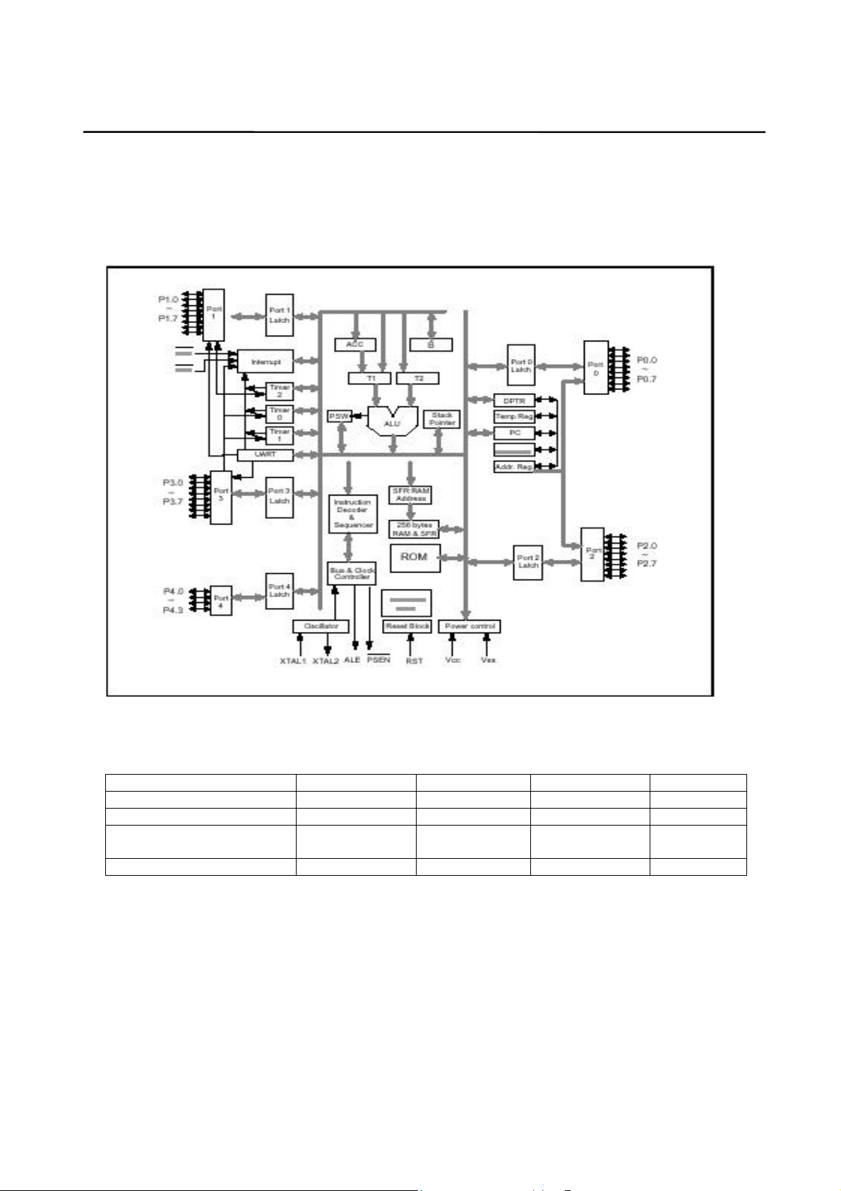
* PIN DESCRIPTION
SYMBOL DESCRIPTIONS
EXTERNAL ACCESS ENABLE: This pin forces the processor to execute out of
EA#
PSEN#
ALE
RST
XTAL1
XTAL2 CRYSTAL2: This is the crystal oscillator output. It is the inversion of XTAL1.
VSS GROUND: Ground potential
VDD POWER SUPPLY: Supply voltage for operation.
P0.0 - P0.7
P1.0 - P1.7
P2.0 - P2.7
P3.0 - P3.7
P4.0 - P4.3
external ROM. It should be kept high to access internal ROM. The ROM address and
data will not be presented on the bus if EA pin is high and the program counter is
within on-chip ROM area.
PROGRAM STORE ENABLE: PSEN enables the external ROM data onto the Port 0
address/ data bus during fetch and MOVC operations. When internal ROM access is
performed, no PSEN strobe signal outputs from this pin.
ADDRESS LATCH ENABLE: ALE is used to enable the address latch that separates
the address from the data on Port 0.
RESET: A high on this pin for two machine cycles while the oscillator is running
resets
the device.
CRYSTAL1: This is the crystal oscillator input. This pin may be driven by an external
clock.
PORT 0: Port 0 is a bi-directional I/O port which also provides a multiplexed low
order
address/data bus during accesses to external memory. The pins of Port 0 can be
individually configured to open-drain or standard port with internal pull-ups.
PORT 1: Port 1 is a bi-directional I/O port with internal pull-ups. The bits have
alternate
functions which are described below:
T2(P1.0): Timer/Counter 2 external count input
T2EX(P1.1): Timer/Counter 2 Reload/Capture control
PORT 2: Port 2 is a bi-directional I/O port with internal pull-ups. This port also
provides the upper address bits for accesses to external memory.
PORT 3: Port 3 is a bi-directional I/O port with internal pull-ups. All bits have alternate
functions, which are described below:
RXD(P3.0) : Serial Port receiver input
TXD(P3.1) : Serial Port transmitter output
INT0 (P3.2) : External Interrupt 0
INT1(P3.3) : External Interrupt 1
T0(P3.4) : Timer 0 External Input
T1(P3.5) : Timer 1 External Input
WR(P3.6) :External Data Memory Write Strobe
RD(P3.7) : External Data Memory Read Strobe
PORT 4: Another bit-addressable bidirectional I/O port P4. P4.3 and P4.2 are
alternative function pins. It can be used as general I/O port or external interrupt input
sources (INT2 / INT3 ).
Page 28
28
Component Descriptions
* BLOCK DIAGRAM
* ABSOLUTE MAXIMUM RATINGS
PARAMETER SYMBOL MIN. MAX. UNIT
DC Power Supply VDD-VSS -0.3 +7.0 V
Input Voltage VIN VSS -0.3 VDD +0.3 V
Operating
Temperature
Storage Temperature TST -55 +150 °C
TA 0 70 °C
Page 29

29
Component Descriptions
2-1-8 Serial EEPROM, 2K (256 x 8) (AT24C02)
* Features
• Low-Voltage and Standard-Voltage Operation
– 5.0 (V CC = 4.5V to 5.5V)
– 2.7 (V CC = 2.7V to 5.5V)
– 2.5 (V CC = 2.5V to 5.5V)
– 1.8 (V CC = 1.8V to 5.5V)
• Internally Organized 128 x 8 (1K), 256 x 8 (2K), 512 x 8 (4K),1024 x 8 (8K) or 2048 x 8 (16K)
• 2-Wire Serial Interface
• Schmitt Trigger, Filtered Inputs for Noise Suppression
• Bidirectional Data Transfer Protocol
• 100 kHz (1.8V, 2.5V, 2.7V) and 400 kHz (5V) Compatibility
• Write Protect Pin for Hardware Data Protection
• 8-Byte Page (1K, 2K), 16-Byte Page (4K, 8K, 16K) Write Modes
• Partial Page Writes Are Allowed
• Self-Timed Write Cycle (10 ms max)
• High Reliability
– Endurance: 1 Million Write Cycles
– Data Retention: 100 Years
– ESD Protection: >3000V
• Automotive Grade and Extended Temperature Devices Available
• 8-Pin and 14-Pin JEDEC SOIC, 8-Pin PDIP, 8-Pin MSOP, and 8-Pin TSSOP Packages
* Pin Configurations
* Pin Description
Pin Name Function
A0 - A2 Address Inputs
SDA Serial Data
SCL Serial Clock Input
WP Write Protect
NC No Connect
Page 30

30
Component Descriptions
2-1-9 4-Megabit (512K x 8) FLASH (A29040)
* Features
• 5.0V±40% for read and write operations
• Access time –70max
• Current
–20 mA typical active read current
–30 mA typical program/erase current
–1µA typical CMOS Standby
• Flexible sector architecture
– 8 uniform sectors of 64 Kbyte each
– Any combination of sectors can be erased
– Supports full chip erase
– Sector protection
• Embedded Erase Algorithms
• Typical 100,000 program/erase cycles per sector
• Compatible with FEDEC-standards
* Pin Configurations
Page 31

31
Component Descriptions
Block Diagram
* Absolute Maximum Ratings*
Ambient Operating Temperature ...................... -55°C to +125°C
Storage Temperature ...................................…. -65°C to +150°C
VOC Ground .……………………………………..-2.0V to +7.0V
Output Voltage…………………………………… -2.0V to +7.0V
Page 32

32
Component Descriptions
2-1-10 512K X 16 Bit X 2 Banks Synchronous DRAM (A43L0616)
Features
n JEDEC standard 3.3V power supply
n LVTTL compatible with multiplexed address
n Dual banks / Pulse RAS
n MRS cycle with address key programs
- CAS Latency (2,3)
- Burst Length (1,2,4,8 & full page)
- Burst Type (Sequential & Interleave)
n All inputs are sampled at the positive going edge of the
n system clock
n Burst Read Single-bit Write operation
n DQM for masking
n Auto & self refresh
n 64ms refresh period (4K cycle)
n 50 Pin TSOP (II)
Pin Configuration
Page 33

33
Component Descriptions
Block Diagram
Pin Descriptions
Symbol Name Description
CLK System Clock Active on the positive going edge to sample all inputs.
CS Chip Select
CKE Clock Enable
A0~A10/AP Address
BA Bank Select Address
RAS Row Address Strobe
CAS Column Address Strobe
WE Write Enable Enables write operation and Row precharge.
L(U)DQM Data Input/Output Mask
DQ0-15
VDD/VSS Power Supply/Ground Power Supply: +3.3V±0.3V/Ground
VDDQ/VSSQ
NC/RFU No Connection
Data Input/Output Data inputs/outputs are multiplexed on the same pins.
Data Output
Power/Ground
Disables or Enables device operation by masking or enabling
all inputs exceptCLK, CKE and L(U)DQM
Masks system clock to freeze operation from the next clock
cycle.
CKE should be enabled at least one clock + tss prior to new
command.
Disable input buffers for power down in standby.
Row / Column addresses are multiplexed on the same pins.
Row address : RA0~RA10, Column address: CA0~CA7
Selects bank to be activated during row address latch time.
Selects band for read/write during column address latch time.
Latches row addresses on the positive going edge of the
CLK with RAS low.
Enables row access & precharge.
Latches column addresses on the positive going edge of the
CLK with CAS low. Enables column access.
Makes data output Hi-Z, t SHZ after the clock and masks the
output.
Blocks data input when L(U)DQM active.
Provide isolated Power/Ground to DQs for improved noise
immunity.
Page 34

34
3. Product Specifications
n Playback System
DVD Video
Video CD (1.1, 2.0, 3.0)
SVCD and CVD
CDDA
CD-ROM with MP3 data
n Television Signal System
NTSC/PAL
n Video Performance
Video Out 1 Vpp into 75 ohm
S-Video Out
Component Out 0.7 Vpp into 75 ohm
D/A Converter 27MHz / 10bit
n Audio Performance
Frequency Response
Output Level
D/A Converter 96KHz/24bit
Y : 1 Vpp into 75 ohm
C : 0.286 Vpp into 75 ohm
DVD : fs 48/96KHz, 4Hz ~
22/44KHz
Video CD : fs 44.1KHz, 4Hz ~
20KHz
Audio CD : fs 44.1KHz, 4Hz ~
20KHz
Analog : 2Vrms (1 KHz)
Digital : 1.15 Vpp
S/N Ratio 110 dB
Page 35

35
AC 90~250V, 50/60Hz
Product Specifications
n Connections
Coaxial digital out X1
Audio Analog out for 2-channel X1
SCART connector for Component Video X1
SCART connector for External Video X1 (option)
Composite Video out X1
S-Video out X1
Optical out X1
n Power Supply
Power Source
n Set
Power Consumption < 25 Watt
Dimensions (W X H X D) 420 X 84 X 270 (mm )
Net Weight 3.6 Kg
Gross Weight 4.9 Kg
Page 36

36
4. Operating Instructions
4-1 Basic Connections
Connecting to audio equipment
Audio equipment
TV set
S-Video cable (optional)
To S-Video input connector
Video/audio cable (supplied)
To video input connector (yellow)
Audio cable (optional)
Connecting to a monaural TV set
Video/audio cable (supplied)
To video input connector (yellow)
Audio cable (optional)
Page 37

37
TV set
To coaxial digital audio input
To optical digital audio input
Operating Instructions
Connecting to a decoder with a Dolby Digital or DTS processing
Video/audio cable (supplied)
Coaxial audio cable (optional)
Optical audio cable (optional)
Decoder or Amplifier with
Front
Subwoofer
Centre
Front
Surround
Connecting to a stereo TV set
Surround
Video/audio cabl(supplied)
To audio input connector (red,
white)To video input connector
(yellow)
S-Video cable
(optional)
Page 38

38
Operating Instructions
4-2 Selecting Video MODE
Press SETUP button and select VIDEO submenu on SETUP screen. After that, select TV type by pressing
DOWN arrow button ( ▼) until desired TV mode is selected. For more information, refer to 7.2 Video on
the Instruction Manual.
4-3 Selecting the desired DVD menu Item
When a DVD disc is loaded, select desired menu item using arrow
button or numeric button, if number for each menu item is displayed,
then press the SELECT button to start play. To select subtitles, the
forth menu item in the figure as shown right, press the RIGHT arrow
button three times and press the SELECT button.
Example:
1. Press the RIGHT arrow button ( ▶ )
2. Press the RIGHT arrow button ( ▶ )
3. Press the RIGHT arrow button ( ▶ )
4. Press the SELECT button
4-4 Selecting the desired MP3 folder
When a MP3 disc is loaded, you may see the menu screen as shown
right. To play a MP3 title, you should select a title under the desired
folder. Use arrow button, select the folder, which you want to play,
by pressing the SELECT button. If you press the SELECT button,
you can see the file lists under the folder. To select DDROST folder
in this case, press the SELECT button.
Example:
1. Press the SELECT button
Page 39

39
Operating Instructions
4-5 Selecting the desired MP3 title
Use arrow button and select an MP3 title using the SELECT button
then play will start automatically. When you know the title number,
enter the MP3 title number using numeric buttons and press the SELECT button. If you want to play an adjacent MP3 title, press the
NEXT button for next title and the PREV button for previous title
during playing. To select “005 HAVEYOU” MP3 title in this case,
press the DOWN arrow button twice and press the SELECT button.
Example:
1. Press the DOWN arrow button ( ▼)
2. Press the DOWN arrow button ( ▼)
3. Press the SELECT button
4-6 Searching
When you want to view the disc contents in fast forward or fast rev erse, you can do that by pressing FF/SF button( ) or FR/SR button
( ). There are total 6 steps for DVD, 4 steps for VCD and 2 steps for
CDDA in fast searching. They are FAST 2X, FAST 4X, FAST 8X,
FAST 16X, FAST 32X and FAST 64X for both direction. To search
at FAST 16X in forward direction, press the FF/SF button 4 times
during play mode.
Example:
1. Press the FF/SF button ( )
2. Press the FF/SF button ( )
3. Press the FF/SF button ( )
4. Press the FF/SF button ( )
4-7 Resume Play
If power is OFF by pressing the POWER button during PLAY or PRESTOP state, play is resumed from the
point where it was stopped. If you switch OFF by disconnecting AC cord, the machine will start playing from
the first track or chapter.
Example:
Press the POWER button during play mode or prestop mode.
Page 40

40
Operating Instructions
4-8 Slow Viewing
When you want to view the disc contents very slowly in forward or
reverse direction, you can do that by pressing the FF/SF button ( )
or the FR/SR button ( ) during pause mode. There are total 3 steps
for DVD and VCD. They are SLOW 1/2X, SLOW 1/4X and SLOW
1/8X for both direction. The slow reverse function is possible only
when a DVD disc is loaded. To view at slow 1/4X in forward direc-
tion, press the FF/SF button ( ) two times during pause mode.
Example:
1. press the PLAY/PAUSE button ( )
1. Press the FF/SF button ( )
2. Press the FF/SF button ( )
4-9 Selecting Audio Language
This function works only with discs on which multiple audio sound
track languages are recorded. If the loaded disc supports multiple
languages, you can see the AUD indicator on fluorescent display.
In the figure shown right, there are total 8 audio languages. To select
the third audio language, press the AUDIO button twice during play.
Example:
1. Press the AUDIO button
2. Press the AUDIO button
4-10 Selecting Subtitle Language
This function works only with discs on which multiple subtitle lan-
gauges are recorded. If the loaded disc supports multiple languages,
you can see the SUB-T indicator on fluorescent display. In the figure
shown right, there is only one subtitle language. To turn on the sub-
title language, press the SUBTITLE button. If you press it again,
you can turn off the subtitle language.
Example:
1. Press the SUBTITLE button
Page 41

41
Operating Instructions
4-11 Selecting Angle
Some DVD discs may contain scenes, which have been shot simultaneously from a number of different angles. If the loaded disc su-
pports multiple angles, you can see indicator on the fluorescent
display and the TV screen. In the figure shown right, there are total
9 angles. To switch to the angle number 2, press the ANGLE button.
Example:
1. Press the ANGLE button
Page 42

42
Operating Instructions
Remained to be defined
Page 43
43
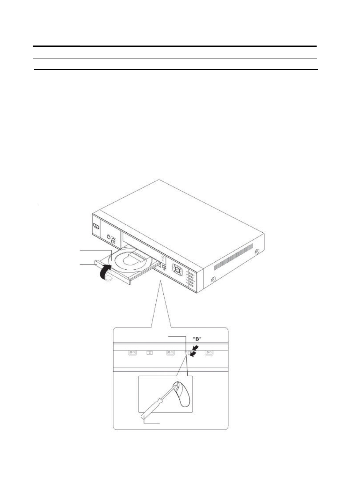
5. Disassembly and Reassembly
¶ Tray
· Door Tray
5-1 Cabinet and PCB
5-1-1 Door Tray Removal
1) Supply Power and open Tray ¶.
2) Disassemble the Door Tray · in direction off arrow “A”.
3) Close Tray ¶ and power off.
Note : If Tray ¶ doesn’t open, insert a Screw driver ¹ into the Emergency hole ¸ (as shown in detailed
drawing) and then turn it in the direction of arrow “B”. Open Tray manually.
¸ Emergency Hole
¹ Screw Driver
<Bottom View>
Fig 5-1 Door Tray Removal
Page 44
44
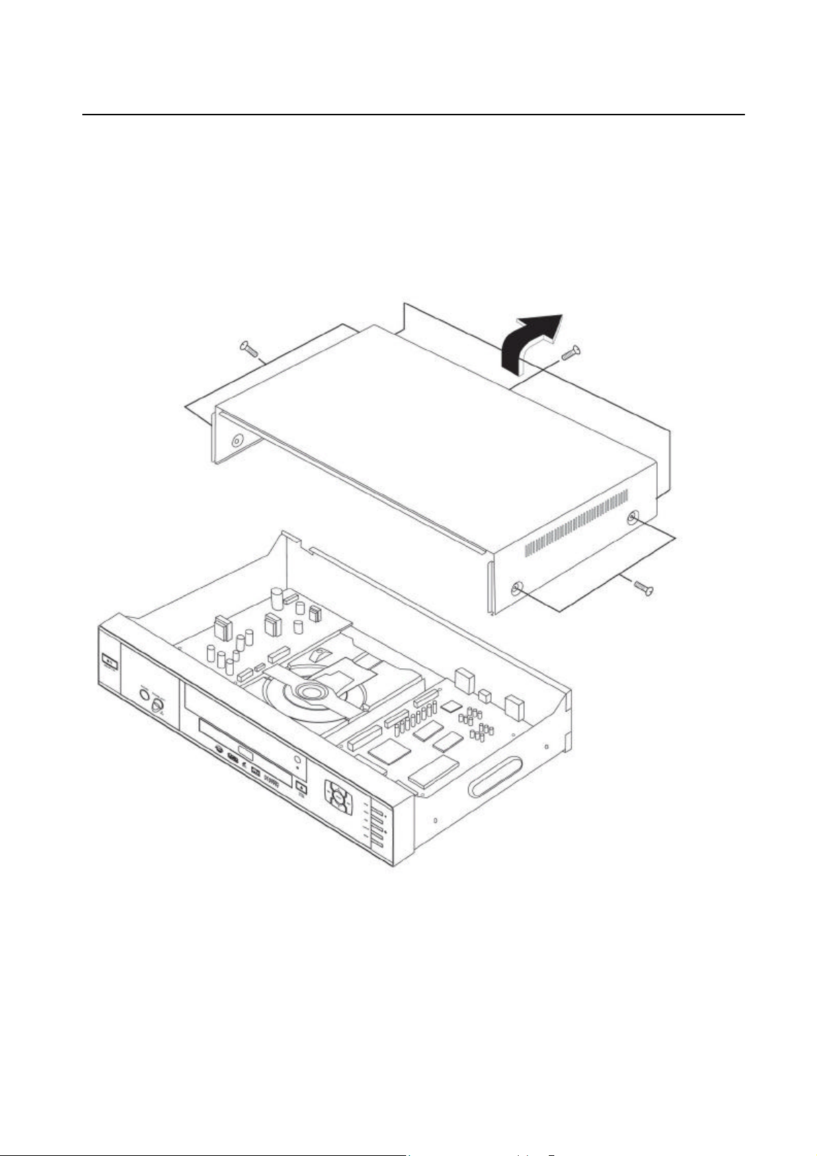
Disassembly and Reassembly
5-1-2 Top Cabinet Removal
1) Remove 3 Screws ¶ on the back Top Cabinet.
2) Remove 2 Screws ·, ¸ on the left and right side.
3) Lift up the Top Cabinet in direction of arrow.
· 2 Screws
¶ 3 Screws
Fig 5-2 Top Cabinet Removal
¸ 2 Screws
Page 45

45
Disassembly and Reassembly
5-1-3 PCB Cable Removal
1) Disconnect PCN1 ¶.
2) Disconnect PCN4 ·.
3) Disconnect LCN1 ¸.
4) Disconnect CON2 ¹.
5) Disconnect CON1 º.
6) Disconnect CON6 ».
7) Disconnect LCN7 ○7.
º CON1
¸ LCN1
¶ PCN1
º CON6
· PCN4
○7LCN7
Fig 5-3 PCB Cable Removal
¹ CON2
Page 46

46
Disassembly and Reassembly
5-1-4 PCB and Front Ass’y Removal
1) Remove 2 Screws ¶ on the back of the Cabinet.
2) Remove 8 Screws · and disassemble the Main PCB ¹ and SMPS PCB º.
3) Remove 5 Screws ¸ and disassemble the Front Ass’y ».
º SMPS PCB
· 8 Screws
¹ Main PCB
» Front Ass’y
¸ 5 Screws
Fig 5-4 PCB and Front Ass’y Removal
Page 47

47
Disassembly and Reassembly
5-1-5 Loader Removal
1) Remove 4 Screws ¶ and disassemble the Loader ·.
¶ 4 Screws
· Loader
Fig 5-5 Loader Removal
Page 48

48
¶ 7 Screws
Disassembly and Reassembly
5-1-6 Front PCB Removal
1) Remove 7 Screws ¶ and disassemble the Front PCB ¸ from the Front Ass’y ·.
`
¸ Front PCB
· Front Ass’y
Fig 5-6 Front PCB Removal
Page 49

49
6. Troubleshooting
Trouble
No power Insert the AC power plug securely into the power outlet.
Action
No picture
No sound Make sure that the equipment is connected properly.
Distorted sound
No fast forward or fast
reverse
No proper aspect ratio
No operations can be
performed with the remote
controller
No button operation
Audio soundtrack and/or
Subtitle language is not the
one you selected.
No Angle change
Make sure that the equipment is connected properly.
Make sure that the input setting for the TV is Video (AV).
Make sure that the input settings for the TV and stereo system are
correct.
Some discs may have sections that prohibit fast forward or fast
reverse.
Select the correct setup for TV aspect ratio that matches your TV
set.
Check the batteries are installed with the correct polarities.
Point the remote control unit at the remote control sensor and
operate.
Remove the obstacles between the remote control unit and remote
control sensor.
Set the POWER button to OFF and then back to ON.
Alternatively, turn off the power, disconnect the power plug and then
reconnect it.
If the audio soundtrack and/or subtitle language does not exist on
the disc, the language selected at the initial settings will not be seen.
This function is dependent on software availability. Even if a disc has
a number of angles recorded, these angles may be recorded for
specific scenes only.
Page 50

50
Troubleshooting
Remained to be defined
Page 51

51
7. Electrical Part List
1.Main board
5.1 Channel Single SCART
NO Spec Pak' Usa' No
ASS'Y MAIN
1 SMPS MANUAL 1
2 Hard Disc Cable, 25mm, 40Pin 1
3 DVD Loader, Mechanism Ass'y Ass'y 1
PCB ASS'Y, MAIN (T/U)
1 80C52(80C51), 40PIN DIP, MPU DIP 1 U701
2 PROGRAM MEMORY 512K * 8 DIP 1 U202
PCB ASS'Y, MAIN (M/I)
1 POWER CON', 12PIN, 2.54mm Strat 1 CON101
2 FRONT CON', WAFER,11PIN, 2.54mm strat 1 CON102
3 BOX HEADER, 20*2, 2.54mm 1 CON103
4 S-VHS CON, MINI DIN, SHILD 1 CON104
2CH Audio CON',6PIN JACK,SHILD, (W-W-Y,R-R-Y)
5
5.1CH Audio CON',6PIN JACK,SHILD, (W-W-B,R-R-B)
6
7 Coaxial CON', 1PIN JACK,SHILD, (B) PCB-L 1 CON108
8 SINGLE SCART, SHIELD,RIGHT ANGLE PCB-L 1 CON105
Sub PCB CON'9PIN, 2.54mm, (Main PCB insert)
9
10 Optical Connector for Audio 1 CON109
11 X-TAL, 11.0592MHZ,HC-49/S, 20pF HC-49/S 1 X601
12 X-TAL, 27MHZ,HC-49/S, 20pF HC-49/S 1 X201
PCB ASS'Y, MAIN (DIP)
1 40PIN, DIP, MPU SOCKET DIP 1 U701
2 32PIN, DIP, ROM SOCKET DIP 1 U202
PCB ASS'Y, MAIN (RAD)
1 ELEC' CAP', 100uF/16V,M 5mm 5 CE101,CE104,CE105,CE106,CE107
2 ELEC' CAP', 100uF/25V,M 5mm 3 CE102,CE103,CE526
3 ELEC' CAP', 10uF/16V,M 5mm 30 CE108,CE109,CE110,CE111,CE201,CE202,CE203,CE204,
4 ELEC' CAP', 10uF/25V,M 5mm 3 CE313,CE314,CE501
5 ELEC' CAP', 47uF/16V,M 5mm 2 CE301,CE401
6 ELEC' CAP', 22uF/16V,M 5mm 20 CE506,CE507,CE508,CE509,CE510,CE511,CE512,CE513,
7 ELEC' CAP', 470uF/25V,M 5mm 1 CE527
PCB ASS'Y, MAIN (SMD)
Location
PCB-L 1 CON106
PCB-L 1 CON107
1 CON110
CE205,CE206,CE207,CE303,CE304,CE305,CE306,CE307,
CE308,CE309,CE310,CE311,CE312,CE315,CE316,CE317,
CE318,CE320,CE321,CE322,CE323,CE701
CE514,CE515,CE516,CE517,CE518,CE519,CE520,CE521,
CE522,CE523,CE524,CE525
Page 52

52
xer, TWO
1 PCB, 2 LAYER FR4 1
2 CPU&RISC SINGLE CHIP PQFP 1 U201
3 Video Encoder, NTSC/PAL LQFP 1 U401
4 16M-SDRAM, 3.3V,400mil,512K*16*2 TSOP(II) 2 U204,U203
5 TTL, HEX INVERTER(FAST) SOIC 1 U206
6 TTL, HEX INVERTER SOIC 1 U207
7 EEPROM, 2KBIT,SOIC SOIC 1 U205
8 Streo DAC,192kHz,24BIt,20Pin SOIC 1 U301
9 Streo DAC,96kHz,24BIt,16Pin SOIC 2 U303,U302
10 DUAL OP-AMP SOIC 7 U304,U305,U306,U307,U308,U309.U310
11 Triple 2-Channel Multiple
SCART
12 WOUND INDUCT', 15uH,3225 SMD 4 L404,L407,L408,L409
13 CHIP POWER BEAD 3216 8 PL101,PL102,PL103,PL104,PL105,PL106,PL107,PL108
14 CHIP FERRITE BEAD 2012 38 EL101,EL102,EL104,EL105,EL106,EL107,EL108,PL109,
15 ZENER DIODE, 3.9V,350mW,SOT-23 SOT-23 1 D504
16 ZENER DIODE, 8.2V,350mW,SOT-23 SOT-23 0
17 Switching diode SOT-23 1 D503
18 Dual Diode, Common kethode SOT-23 4 D501,D502,D508,D509
19 RLS4148 SOT-23 1 D701
20 GENERAL TR, NPN SOT-23 37 Q501,Q502,Q504,Q506,Q507,Q508,Q509,Q510,Q511,
21 GENERAL TR, PNP SOT-23 0
22 Switching TR, NPN SOT-23 5 Q538,Q539,Q541,Q544,Q701
23 Switching TR, PNP SOT-23 5 Q540,Q542,Q545,Q550,Q702
24 CHIP RES', 1/10W,0 ΩJ 1608 14 R107,R203,R207,R209,R245,R252,R265,R406,
25 CHIP RES', 1/10W,10 ΩJ 1608 13 R202,R253,R254,R255,R256,R257,R258,R259,R260,
26 CHIP RES', 1/10W,100 ΩJ 1608 12 R561,R566,R571,R576,R581,R586,R591,R596,R601,
27 CHIP RES', 1/10W,1K ΩJ 1608 13 R266,R267,R507,R509,R514,R560,R562,R565,R567,
28 CHIP RES', 1/10W,10K ΩJ 1608 7 R350,R355,R358,R360,R701,R712,R715
29 CHIP RES', 1/10W,100K ΩJ 1608 33 R519,R522,R524,R527,R529,R532,R534,R537,R539,
30 CHIP RES', 1/10W,1M ΩJ 1608 3 R268,R269,R275
31 CHIP RES', 1/10W,22 ΩJ 1608 23 ER201,ER202,R301,R302,R303,R304,R305,R306,R307,
32 CHIP RES', 1/10W,220 ΩJ 1608 8 R270,R271,R272,R273,R274,R620,R621,R702
33 CHIP RES', 1/10W,33 ΩJ 1608 28 R219,R220,R221,R222,R223,R224,R225,R226,R227,
34 CHIP RES', 1/10W,330 ΩJ 1608 2 R103,R104
DMP 0
EL109,PL110,EL110,PL111,PL112,PL201,PL202,PL301,
PL401,PL303,PL304,PL502,EL501,EL502,EL503,EL504,
EL505,EL506,EL507,EL508,EL509,EL510,EL511,EL512,
EL513,EL514,EL515,EL516,EL517,EL518
Q512,Q513,Q514,Q515,Q516,Q517,Q518,Q519,Q520,
Q521,Q522,Q523,Q524,Q525,Q526,Q527,Q528,Q529,
Q530,Q531,Q532,Q533,Q534,Q535,Q536,Q537,Q546,
Q547
R501~R506
R261,R262,R263,R264
R606,R611,R616
R628,R629,R630,R631
R542,R544,R547,R549,R552,R554,R557,R558,R563,
R568,R573,R578,R583,R588,R593,R598,R603,R608,
R613,R632
R308,R309,R310,R311,R312,R313,R314,R315,
R316,R317,R318,R319,R320,R321
R228,R229,R230,R231,R232,R233,R234,R235,
R236,R237,R238,R246,R247,R248,R249,R250,R251,
R401,R402
Page 53

53
BC234,BC235,BC236,BC237,BC238,BC240,BC301,BC303,
35 CHIP RES', 1/10W,3.3K ΩJ 1608 27 R201,R334,R342,R345,R347,R361,R405,R520,R525,
R530,R535,R540,R545,R550,R555,R618,R619,R703,
R705,R706,R707,R708,R709,R710,R713,R714,R717
36 CHIP RES', 1/10W,47 ΩJ 1608 9 R211,R212,R213,R214,R215,R216,R217,R218,R508
37 CHIP RES', 1/10W,470 ΩJ 1608 1 R404
38 CHIP RES', 1/10W,47K ΩJ 1608 2 R239,R240
39 CHIP RES', 1/10W,4.7K ΩJ 1608 9 R101,R102,R204,R241,R242,R243,R510,R511,R515
40 CHIP RES', 1/10W,5.6K ΩJ 1608 12 R322,R323,R324,R325,R326,R328,R330,R332,R349,
R352,R354,R357
41 CHIP RES', 1/10W,620 ΩJ 1608 8 R407,R408,R413,R414,R415,R416,R417,R418
42 CHIP RES', 1/10W,6.2K ΩJ 1608 2 R346,R348
43 CHIP RES', 1/10W,75 ΩJ 1608 9 R521,R526,R531,R536,R541,R546,R551,R556,R633
44 CHIP RES', 1/10W,91 ΩJ 1608 1 R106
45 CHIP RES', 1/10W,1.2K ΩJ 1608 4 R327,R329,R331,R333
46 CHIP RES', 1/10W,1.3K ΩJ 1608 20 R570,R572,R575,R577,580,R582,R585,R587,R590,
R592,R595,R597,R600,R602,R605,R607,R610,R612,
R615,R617
46 CHIP RES', 1/10W,3.9K ΩJ 1608 6 R339,R343,R351,R353,R356,R359
47 CHIP RES', 1/10W,15K ΩJ 1608 1 R716
48 CHIP RES', 1/10W,20K ΩJ 1608 8 R538,R543,R548,R553, R518,R523,R528,R533
49 CHIP RES', 1/10W,300 ΩJ 1608 12 R559,R564,R569,R574,R579,R584,R589,R594,R599,R60
4,R609,R614
50 CHIP RES', 1/10W,9.31K ΩF 1608 3 R362,R363,R364
51 CHIP RES', 1/10W,18.7K ΩF 1608 3 R365,R366,R367
52 CHIP CAP', 25V,3pF,J,COG 1608 4 C402,C411,C414,C417
53 CHIP CAP', 25V,22pF,J,COG 1608 1 C202
54 CHIP CAP', 25V,2700pF,J,COG 1608 8 C302,C303,C304,C305,C310,C312,C314,C316
55 CHIP CAP', 25V,27pF,J,COG 1608 16 C203,C207,C208,C210,C211,C212,C403,C404,C412,
C413,C415,C416,C418, C419,C701,C702
56 CHIP CAP', 25V,33pF,J,COG 1608 6 C201,C220,C221,C222,C223,C224
57 CHIP CAP', 25V,330pF,J,COG 1608 4 C313,C315,C317,C321
58 CHIP CAP', 25V,47pF,J,COG 1608 10 TC201,C501,C502,C503,C504,C505,C506,C507,C508,
C530
59 CHIP CAP', 25V,470pF,J,COG 1608 12 C509,C510,C511,C512,C513,C514,C515,C516,C517,
C518,C519,C520
60 CHIP CAP', 25V,560pF,J,COG 1608 4 C306,C307,C308,C309
61 CHIP CAP', 25V,15pF,J,COG 1608 29 EC101,EC103,EC104,EC105,EC106,EC107,EC108,EC109,
EC110,EC111,C205,EC501,EC502,EC503,
EC504,EC505,EC506,EC507,EC508,EC509,EC510,EC511,
EC512,EC513,EC514,EC515,EC516,EC517,EC518
62 CHIP CAP', 25V,0.1uF,Z,Y5V 1608 98 BC101,BC102,BC103,C104,BC104,BC105,BC106,BC107,
BC108,BC109,BC110,BC111,BC112,BC200,BC201,BC202,
BC203,BC204,BC205,C206,BC206,BC207,BC208,BC209,
BC210,BC211,BC212,BC213,BC214,BC215,BC216,BC217,
BC218,BC219,BC220,BC221,BC222,BC223,BC224,BC225,
BC226,BC227,BC228,BC229,BC230,BC231,BC232,BC233,
BC304,BC305,BC306,BC307,BC308,BC309,BC310,BC311,
BC312,BC313,BC314,BC315,BC316,BC317,BC318,BC319,
BC320,BC321,BC322,BC323,BC325,BC326,BC327,BC328,
BC329,BC330,BC331,BC332,BC333,BC334,BC401,C422,
C423,C424,C425,C426,C427,C428,BC501,BC506,BC507,
BC701
Page 54

54
5.1CH Audio CON',6PIN JACK,SHILD,
Sub PCB CON'9PIN, 2.54mm, (Main PCB
5.1 Channel Dual SCART
NO Spec Pak' Usa' No
ASS'Y MAIN
1 SMPS MANUAL 1
2 Hard Disc Cable, 25mm, 40Pin 1
3 DVD Loader, Mechanism Ass'y Ass'y 1
PCB ASS'Y, MAIN (T/U)
1 80C52(80C51), 40PIN DIP, MPU DIP 1 U701
2 PROGRAM MEMORY 512K * 8 DIP 1 U202
PCB ASS'Y, MAIN (M/I)
1 POWER CON', 12PIN, 2.54mm Strat 1 CON101
2 FRONT CON', WAFER,11PIN, 2.54mm strat 1 CON102
3 BOX HEADER, 20*2, 2.54mm 1 CON103
4 S-VHS CON, MINI DIN, SHILD 1 CON104
5 2CH Audio CON',6PIN JACK,SHILD, (W-
W-Y,R-R-Y)
6
(W-W-B,R-R-B)
7 Coaxial CON', 1PIN JACK,SHILD, (B) PCB-L 1 CON108
8 DUAL SCART, SHIELD,RIGHT ANGLE PCB-L 1 CON105
9
insert)
10 Optical Connector for Audio 1 CON109
11 X-TAL, 11.0592MHZ,HC-49/S, 20pF HC-49/S 1 X601
12 X-TAL, 27MHZ,HC-49/S, 20pF HC-49/S 1 X201
PCB ASS'Y, MAIN (DIP)
1 40PIN, DIP, MPU SOCKET DIP 1 U701
2 32PIN, DIP, ROM SOCKET DIP 1 U202
PCB ASS'Y, MAIN (RAD)
1 ELEC' CAP', 100uF/16V,M 5mm 5 CE101,CE104,CE105,CE106,CE107
2 ELEC' CAP', 100uF/25V,M 5mm 3 CE102,CE103,CE526
3 ELEC' CAP', 10uF/16V,M 5mm 30 CE108,CE109,CE110,CE111,CE201,CE202,CE203,CE204,
4 ELEC' CAP', 10uF/25V,M 5mm 5 CE313,CE314,CE501,CE504,CE505
5 ELEC' CAP', 47uF/16V,M 5mm 2 CE301,CE401
6 ELEC' CAP', 22uF/16V,M 5mm 20 CE506,CE507,CE508,CE509,CE510,CE511,CE512,CE513,
7 ELEC' CAP', 470uF/25V,M 5mm 1 CE527
PCB ASS'Y, MAIN (SMD)
Location
PCB-L 1 CON106
PCB-L 1 CON107
1 CON110
CE205,CE206,CE207,CE303,CE304,CE305,CE306,CE307,
CE308,CE309,CE310,CE311,CE312,CE315,CE316,CE317,
CE318,CE320,CE321,CE322,CE323,CE701
CE514,CE515,CE516,CE517,CE518,CE519,CE520,CE521,
CE522,CE523,CE524,CE525
Page 55

55
1 PCB, 2 LAYER FR4 1
2 CPU&RISC SINGLE CHIP PQFP 1 U201
3 Video Encoder, NTSC/PAL LQFP 1 U401
4 16M-SDRAM, 3.3V,400mil,512K*16*2 TSOP(II) 2 U204,U203
5 TTL, HEX INVERTER(FAST) SOIC 1 U206
6 TTL, HEX INVERTER SOIC 1 U207
7 EEPROM, 2KBIT,SOIC SOIC 1 U205
8 Streo DAC,192kHz,24BIt,20Pin SOIC 1 U301
9 Streo DAC,96kHz,24BIt,16Pin SOIC 2 U303,U302
10 DUAL OP-AMP SOIC 7 U304,U305,U306,U307,U308,U309.U310
Triple 2-Channel Multiplexer, TWO SCART
11
12 WOUND INDUCT', 15uH,3225 SMD 4 L404,L407,L408,L409
13 CHIP POWER BEAD 3216 8 PL101,PL102,PL103,PL104,PL105,PL106,PL107,PL108
14 CHIP FERRITE BEAD 2012 38 EL101,EL102,EL104,EL105,EL106,EL107,EL108,PL109,
15 ZENER DIODE, 3.9V,350mW,SOT-23 SOT-23 1 D504
16 ZENER DIODE, 8.2V,350mW,SOT-23 SOT-23 2 D506.D507
17 Switching diode SOT-23 1 D503
18 Dual Diode, Common kethode SOT-23 4 D501,D502,D508,D509
19 RLS4148 SOT-23 1 D701
20 GENERAL TR, NPN SOT-23 40 Q501,Q502,Q503,Q504,Q505,Q506,Q507,Q508,Q509,
21 GENERAL TR, PNP SOT-23 1 Q543
22 Switching TR, NPN SOT-23 6 Q538,Q539,Q541,Q544.Q549,Q701
23 Switching TR, PNP SOT-23 5 Q540,Q542,Q545,Q550,Q702
24 CHIP RES', 1/10W,0 ΩJ 1608 8 R107,R203,R207,R209,R245,R252,R265,R406
25 CHIP RES', 1/10W,10 ΩJ 1608 13 R202,R253,R254,R255,R256,R257,R258,R259,R260,
26 CHIP RES', 1/10W,100 ΩJ 1608 12 R561,R566,R571,R576,R581,R586,R591,R596,R601,
27 CHIP RES', 1/10W,1K ΩJ 1608 18 R266,R267,R507,R509,R512,R514,R516,R560,R562,
28 CHIP RES', 1/10W,10K ΩJ 1608 7 R350,R355,R358,R360,R701,R712,R715
29 CHIP RES', 1/10W,100K ΩJ 1608 33 R518,R519,R522,R523,R524,R527,R528,R529,R532,
30 CHIP RES', 1/10W,1M ΩJ 1608 3 R268,R269,R275
31 CHIP RES', 1/10W,22 ΩJ 1608 23 ER201,ER202,R301,R302,R303,R304,R305,R306,R307,
32 CHIP RES', 1/10W,220 ΩJ 1608 8 R270,R271,R272,R273,R274,R620,R621,R702
33 CHIP RES', 1/10W,33 ΩJ 1608 28 R219,R220,R221,R222,R223,R224,R225,R226,R227,
34 CHIP RES', 1/10W,330 ΩJ 1608 2 R103,R104
35 CHIP RES', 1/10W,3.3K ΩJ 1608 27 R201,R334,R342,R345,R347,R361,R405,R520,R525,
DMP 2 U501,U502
EL109,PL110,EL110,PL111,PL112,PL201,PL202,PL301,
PL401,PL303,PL304,PL501,EL501,EL502,EL503,EL504,
EL505,EL506,EL507,EL508,EL509,EL510,EL511,EL512,
EL513,EL514,EL515,EL516,EL517,EL518
Q510,Q511,Q512,Q513,Q514,Q515,Q516,Q517,Q518,
Q519,Q520,Q521,Q522,Q523,Q524,Q525,Q526,Q527,
Q528,Q529,Q530,Q531,Q532,Q533,Q534,Q535,Q536,
Q537,Q546,Q547,Q548
R261,R262,R263,R264
R606,R611,R616
R565,R567,R626,R627,R628,R629, R630,R631,R634
R533,R534,R537,R539,R542,R544,R547,R549,R552,
R554,R557,R558,R563,R568,R573,R578,R583,R588,
R593,R598,R603,R608,R613,R632
R308,R309,R310,R311,R312,R313,R314,R315,R316,
R317,R318,R319,R320,R321
R228,R229,R230,R231,R232,R233,R234,R235,R236,
R237,R238,R246,R247,R248,R249,R250,R251,R401,R402
R530,R535,R540,R545,R550,R555,R618,R619,R703,
R705,R706,R707,R708,R709,R710,R713,R714,R717
Page 56

56
BC234,BC235,BC236,BC237,BC238,BC240,BC301,BC303,
36 CHIP RES', 1/10W,47 ΩJ 1608 9 R211,R212,R213,R214,R215,R216,R217,R218,R508
37 CHIP RES', 1/10W,470 ΩJ 1608 1 R404
38 CHIP RES', 1/10W,47K ΩJ 1608 2 R239,R240
39 CHIP RES', 1/10W,4.7K ΩJ 1608 11 R101,R102,R204,R241,R242,R243,R510,R511,R513,R515
,R517
40 CHIP RES', 1/10W,5.6K ΩJ 1608 12 R322,R323,R324,R325,R326,R328,R330,R332,R349,
R352,R354,R357
41 CHIP RES', 1/10W,620 ΩJ 1608 8 R407,R408,R413,R414,R415,R416,R417,R418
42 CHIP RES', 1/10W,6.2K ΩJ 1608 2 R346,R348
43 CHIP RES', 1/10W,75 ΩJ 1608 9 R521,R526,R531,R536,R541,R546,R551,R556,R633
44 CHIP RES', 1/10W,91 ΩJ 1608 1 R106
45 CHIP RES', 1/10W,1.2K ΩJ 1608 4 R327,R329,R331,R333
46 CHIP RES', 1/10W,1.3K ΩJ 1608 20 R570,R572,R575,R577,580,R582,R585,R587,R590,R592,
R595,R597,R600,R602,R605,R607,R610,
R612,R615,R617
46 CHIP RES', 1/10W,3.9K ΩJ 1608 6 R339,R343,R351,R353,R356,R359
47 CHIP RES', 1/10W,15K ΩJ 1608 1 R716
48 CHIP RES', 1/10W,20K ΩJ 1608 4 R538,R543,R548,R553
49 CHIP RES', 1/10W,300 ΩJ 1608 12 R559,R564,R569,R574,R579,R584,R589,R594,R599,R604
,R609,R614
50 CHIP RES', 1/10W,9.31K ΩF 1608 3 R362,R363,R364
51 CHIP RES', 1/10W,18.7K ΩF 1608 3 R365,R366,R367
52 CHIP CAP', 25V,3pF,J,COG 1608 4 C402,C411,C414,C417
53 CHIP CAP', 25V,22pF,J,COG 1608 1 C202
54 CHIP CAP', 25V,2700pF,J,COG 1608 8 C302,C303,C304,C305,C310,C312,C314,C316
55 CHIP CAP', 25V,27pF,J,COG 1608 16 C203,C207,C208,C210,C211,C212,C403,C404,C412,C413
,C415,C416,C418, C419,C701,C702
56 CHIP CAP', 25V,33pF,J,COG 1608 6 C201,C220,C221,C222,C223,C224
57 CHIP CAP', 25V,330pF,J,COG 1608 4 C313,C315,C317,C321
58 CHIP CAP', 25V,47pF,J,COG 1608 10 TC201,C501,C502,C503,C504,C505,C506,C507,C508,
C530
59 CHIP CAP', 25V,470pF,J,COG 1608 12 C509,C510,C511,C512,C513,C514,C515,C516,C517,C518
,C519,C520
60 CHIP CAP', 25V,560pF,J,COG 1608 4 C306,C307,C308,C309
61 CHIP CAP', 25V,15pF,J,COG 1608 29 EC101,EC103,EC104,EC105,EC106,EC107,EC108,EC109,
EC110,EC111,C205,EC501,EC502,EC503,
EC504,EC505,EC506,EC507,EC508,EC509,EC510,EC511,
EC512,EC513,EC514,EC515,EC516,EC517,EC518
62 CHIP CAP', 25V,0.1uF,Z,Y5V 1608 102 BC101,BC102,BC103,C104,BC104,BC105,BC106,BC107,
BC108,BC109,BC110,BC111,BC112,BC200,BC201,BC202,
BC203,BC204,BC205,C206,BC206,BC207,BC208,BC209,
BC210,BC211,BC212,BC213,BC214,BC215,BC216,BC217,
BC218,BC219,BC220,BC221,BC222,BC223,BC224,BC225,
BC226,BC227,BC228,BC229,BC230,BC231,BC232,BC233,
BC304,BC305,BC306,BC307,BC308,BC309,BC310,BC311,
BC312,BC313,BC314,BC315,BC316,BC317,BC318,BC319,
BC320,BC321,BC322,BC323,BC325,BC326,BC327,BC328,
BC329,BC330,BC331,BC332,BC333,BC334,BC401,C422,
C423,C424,C425,C426,C427,C428,BC501,BC502,BC503,
BC504,BC505, BC506,BC507,BC701
Page 57

57
N(PCB), PCB
2. Headphone board
PCB ASS'Y, HEADPHONE (M/I)
1 HEADPHONE WIRE, 9PIN-9PI
IN
2 HEADPHONE JACK 1 JAC901
3 VARIABLE RESISTOR
PCB ASS'Y, HEADPHONE (RAD)
1 ELEC' CAP', 22uF/16V,M 5mm 2 CE902,CE901
2 ELEC' CAP', 47uF/25V,M 5mm 2 CE903,CE904
PCB ASS'Y, HEADPHONE (SMD)
1 HEADPHONE PCB 1LAYER FR1 1
2 CHIP CAP', 25V,470pF,J,COG 1608 2 C901,C903
3 CHIP CAP', 25V,100pF,J,COG 1608 2 C902,C904
4 CHIP CAP', 25V,0.1uF,Z,Y5V 1608 2 C906,C905
5 CHIP FERRITE BEAD 2012 2 L901,L902
6 GENERAL TR, NPN SOT-23 4 Q901,Q902,Q903,Q904
7 CHIP RES', 1/10W,100 ΩJ 0603 4 R902,R907,R904,R909
8 CHIP RES', 1/10W,1 K ΩJ 0603 4 R903,R905,R908,R910
9 CHIP RES', 1/10W, 10K ΩJ 0603 1 R915
10 CHIP RES', 1/10W,100K ΩJ 0603 2 R901,R906
11 CHIP RES', 1/10W, 3.3K ΩJ 0603 2 R911,R913
12 CHIP RES', 1/10W, 6.2K ΩJ 0603 2 R912,R914
13 DUAL OP-AMP SOIC 1 U901
Total
WIRE 1 CON901
1 VR901
3. Front Board
NO
PCB ASS'Y, FRONT (T/U)
PCB ASS'Y, FRONT (M/I)
1 (IR)INFRA RECIEVER L Type 1 U2
2 TR TO-92 1 Q1
3 VFD DISPLAY 1 U3
4 FrontPowerWire, 5Pin-5Pin(PCB), PCB IN WIRE 1 CON2
5 FrontSignalWire,11Pin-11Pin(PCB),PCB IN WIRE 1 CON1
6 TACT S/W, 4PIN,5mm 5mm 11
PCB ASS'Y, FRONT (RAD)
1 LED,RED, 3 PIE, 5mm Formming, High 4.5mm 1 D2
2 ELEC' CAP', 10uF/16V,M 5mm 2 CE1,CE2,CE4
3 ELEC' CAP', 10uF/50V,M 5mm 1 CE3
PCB ASS'Y, FRONT (AXI)
1 PCB, 1 LAYER FR1 1 REV. C+
2 JUMPER 8mm 9 JP1,JP16,JP17,JP23,JP24,JP25,JP26,JP27,JP28
3 JUMPER 12mm 17 JP2,JP4~15,JP18~JP21
4 JUMPER 18mm 2 JP3,JP22
5 DIODE AXIAL 3 D3,D4,D5
6 Axial Cap, 50V,0.IUF,Z AXIAL 7 C1,C3,C4,C5,C6,C7,C8
7 AXIAL,BEAD, 3560 AXIAL 2 L1,L2
8
AXI' RES', 1/8W,3.3K ΩJ
Spec' & description Pak' Usa' Location No.
SW1,SW2,SW3,SW4,SW5,SW6,SW8,SW9,SW10,
SW11,SW12
AXIAL 1 R9
Page 58

58
9
AXI' RES', 1/8W,56K ΩJ
10
AXI' RES', 1/6W,10K ΩJ
11
AXI' RES', 1/6W,330 ΩJ
12
AXI' RES', 1/6W,22 ΩJ
PCB ASS'Y, FRONT BOTTUM (SMD)
1 VFD DRIVER PQFP 1 U1
AXIAL 1 R12
AXIAL 6 R3,R4,R5,R6,R7,R8
AXIAL 1 R1
AXIAL 1 NR1
4. SMPS PART LIST
NO
PCB ASS'Y, SMPS (RAD)
1 ELEC' CAP', 220uF/6.3V,M 6mm 2 PC14,15
2 ELEC' CAP', 220uF/16V,M 8mm 3 PC16,28,30
3 ELEC' CAP', 470uF/16V,M 10mm 3 PC6,10,11
4 ELEC' CAP', 10uF/50V,M 5mm 1 PC32
5 ELEC' CAP', 47uF/35V,M 6mm 1 PC17
6 ELEC' CAP', 470uF/6.3V,M 8mm 4 PC13,19,22,25
7 ELEC' CAP', 1000uF/6.3V,M 10mm 3 PC12,18,33
8 ELEC' CAP', 47uF/16V,M 5mm 1 PC34
9 ELEC' CAP', 220uF/25V,M 5mm 1 PC8
10 ELEC' CAP', 22uF/16V,M 5mm 1 PC40
11 ELEC' CAP', 1uF/50V,M 5mm 3 PC21,26,29
12 PE-CAP',YSG472J2AN 5mm 3 PC3,23,61
13 PE-CAP',PEA102J2AN 5mm 2 PC24,60
14 PE-CAP',PEA103J2AN 5mm 1 PC7
15 PE-CAP',PEA682J2AN 5mm 1 PC5
16 FRD', FR103 4 PD9,14,16,17
17 FRD', FR204 1 PD7
18 FRD', FR107 2 PD5,6
19 FRD', FR154 1 PD11
20 SRD', SR204 1 PD10
21 RECTIFIER', 1N4007 6 PD1,2,3,4,18,19
22 ZENER', 1N5252(500mW) DO-35 3 PZD2,5,6
23 ZENER', 1N5234(500mW) DO-35 1 PZD4
24 ZENER', 1N5242(500mW) DO-35 3 PZD1,3,7
PCB ASS'Y, SMPS (AXI)
1 PCB, 1 LAYER FR1 1
2
RES-RD', 1/8W,10 ΩJ
3
RES-RD', 1/8W,47K ΩJ
4
RES-RD' 1/8W,10K ΩJ
5
RES-RD', 1/8W,220 ΩJ
6
RES-RD', 1/8W,22K ΩJ
7
RES-RD', 1/8W,150 ΩJ
8
RES-RD', 1/8W,27K ΩJ
9
RES-RD', 1/8W,51 ΩJ
10
RES-RD', 1/8W,1K ΩJ
11
RES-RD', 1/8W,100 ΩJ
12
RES-RD', 1/8W,18K ΩJ
13
RES-RD', 1/8W,4.7K ΩJ
14
RES-RD', 1/8W,470 ΩJ
15
RES-CF', 1/8W,560 ΩJ
Spec Pak' Usa' No
2 PR6,21
3 PR1,9,42
3 PR7,16,18
2 PR38,43
1 PR3
1 PR33
2 PR5,17
1 PR26
2 PR32,39
2 PR25,30
1 PR22
2 PR36,40
4 PR11,12,15,19
1 PR35
Page 59
59
16
RES-RD', 1/4W,2K ΩJ
17
RES-RD', 1/8W,4.7K ΩJ
18
RES-RD', 1/8W,6.8K ΩJ
19
RES-RD', 1/4W,270K ΩJ
NO
20
RES-RN', 1/8W,2K ΩJ F
21
RES-RN', 1/8W,12K ΩJ F
22
RES-RN', 1/8W,6.8K ΩJ F
23
RES-MOF', 2W,15 ΩJ (MOR)
24 CER.CAP', 102K 1KV 2 PC4,9
25 CER.CAP', 471K 50V 2 PC27,57
26 KSP2222ATA TO-92 5 PQ2,4,5,6,7
27 KIA431 TO-92 2 PU2,3
28 PN2907 TO-92 1 PQ8
29 THERMISTER’, 5D-9 1 PTH1
30 CHOKE', PEAKING 10uH 5 PL3,4,6,8,10,
PCB ASS'Y, SMPS (M/I)
1 MOS FET', IRF 830 T0-220 2 PQ1,3
2 VTG REGULATER KA7805 T0-220 1 PU9
3 VTG REGULATER KA7812 T0-220 1 PU4
4
ELEC' CAP', 47uF/400,(105℃)
5 250VAC 104 1 PC1
6 FRD’ SF34 1 PD8
7 TCET 1103 2 PU1,6
8
RES-MOF', 2W,1K ΩJ(MOR)
9
RES-MOF', 2W,12K ΩJ(MOR)
10
RES-MOF', 2W,470 ΩJ(MOR)
11 Y-CAP', 332 Y-1 1 PC20
12 TRANS', EER2229 1 PT1
13 TRANS', EER2828 1 PT2
14 LINEFILTER', UU 1116(40mH) 1 PL1
15 FUSE', 250T 2.0A 1 PF1
16 FUSE CLIP', PLASTIC 1
17 RUBBER', BAR 1
18
절연지', SIZE 50*35
19 CONN ASS'Y', 12PIN, 350mm PCB IN WIRE 1 PCN2
20 CONN ASS'Y', 4PIN, 220mm PCB IN WIRE 1 PCN3
21 WAFER,5PIN(SMALL) PCB IN WAFER 1 PCN4
22 PIN POST', 2PIN 10mm
Spec Pak' Usa' No
3 PR10,13,29
1 PR36
1 PR41
2 PR2,28
3 PR23,31,37
1 PR45
1 PR34
2 PR44,46
1 PC2
2 PR4,47
2 PR8,20
1 PR27
1
PIN
POST'
1 PCN5
Page 60

60
Electrical Part List
Remained to be defined
Page 61

61
8. Block Diagram
MAIN PCB
POWER
PCB
HEAD PHONE
PCB
LOADER
(DVS)
VFD
REMOCON
EYE
VIDEO
ENCODER
A/V
DECODER
&
MAIN CPU
KEY
MATRIX
D/A
CONVERTE
R
SUB
MICOM
RCU
FRONT PCB
Page 62

62
Block Diagram
Remained to be defined
Page 63

63
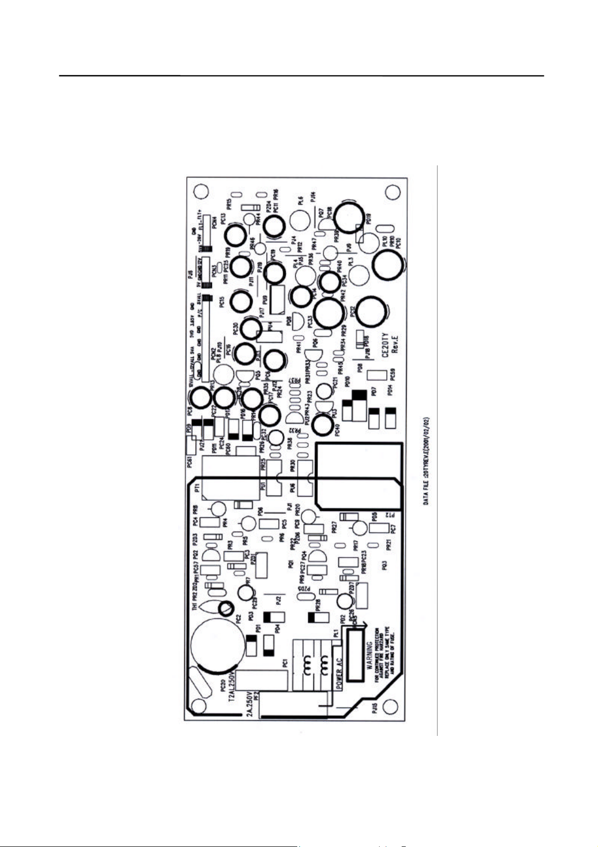
9. PCB Diagrams
9-1 Main PCB (Component Side)
Page 64

64
PCB Diagrams
9-2 Main PCB (Solder Side)
Page 65

65
PCB Diagrams
9-3 Front PCB (Component Side) 9-4 Front PCB (Solder Side)
Page 66
66
PCB Diagrams
9-5 SMPS PCB (Top Side)
Page 67

67
PCB Diagrams
9-6 SMPS PCB (Bottom Side)
Page 68

68
10. Wiring Diagram
Page 69

69
Wiring Diagram
Remained to be defined
Page 70

70
11. Schematic Diagrams
11-1 Main PCB Schematic Diagram
11-1-1 Main PCB Top Schematic diagram
Page 71

71
Schematic Diagrams
11-1-2 Main PCB A/V Decoder Block Schematic diagram
Page 72

72
Schematic Diagrams
11-1-3 Main PCB Submicom Block Schematic diagram
Page 73

73
Schematic Diagrams
11-1-4 Main PCB Video Block Schematic diagram
Page 74

74
Schematic Diagrams
11-1-5 Main PCB Audio Block Schematic diagram
Page 75

75
Schematic Diagrams
11-1-6 Main PCB Out Stage Block Schematic diagram
Page 76
76
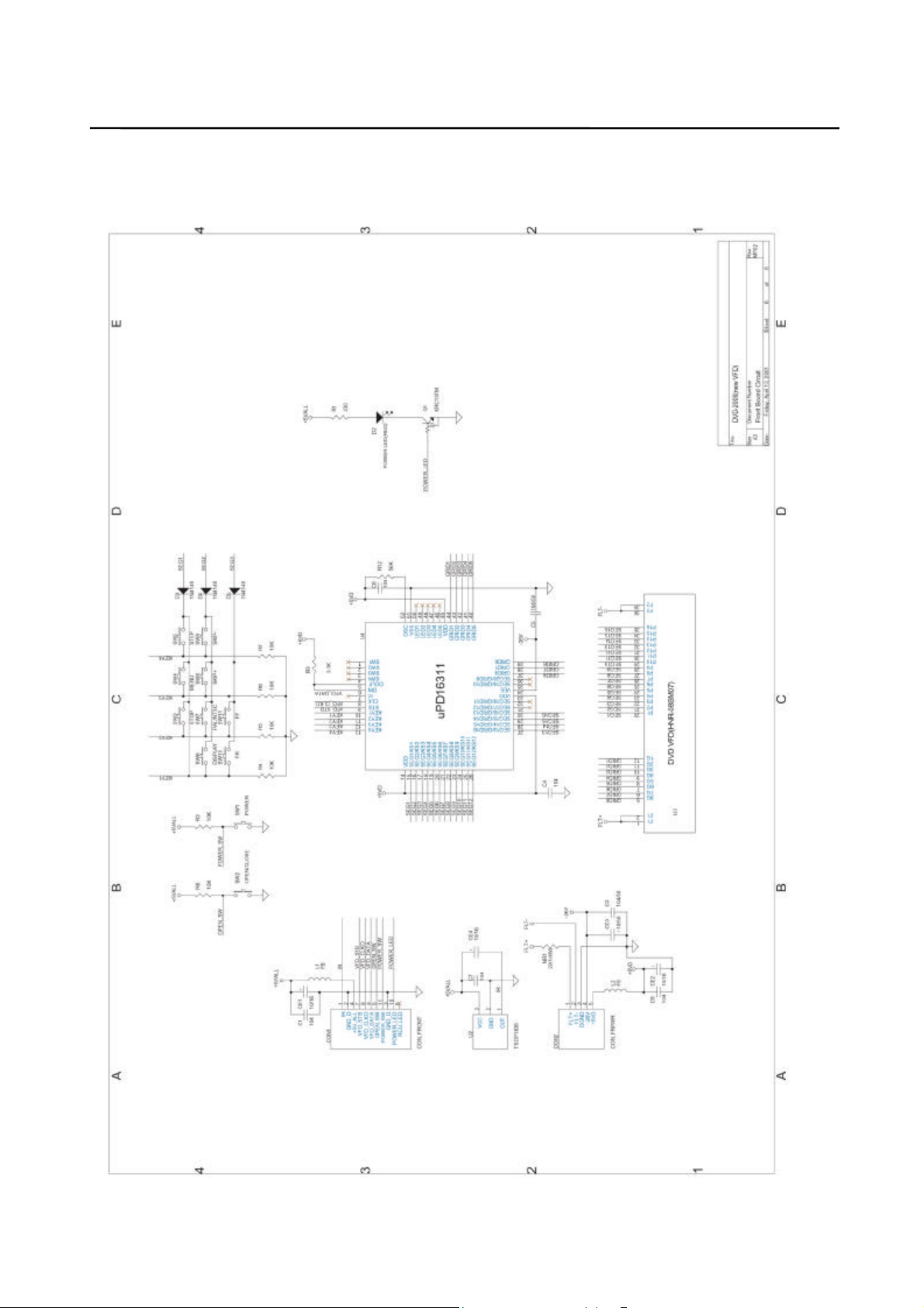
11-2 Front PCB Schematic Diagram
11-2-1 Front PCB Schematic diagram
Page 77
77
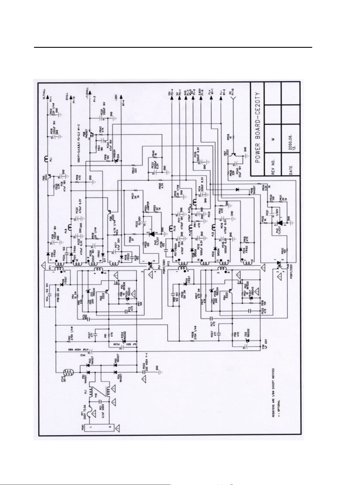
11-3 SMPS PCB Schematic Diagram
Page 78

78
Schematic Diagrams
Remained to be defined
Page 79

79
TaeYoung Telstar Co.,Ltd May.2001
Printed in Korea
 Loading...