

Cypress Semiconductor CY7C466A-25PTC, CY7C466A-25JC, CY7C460A-10PC, CY7C460A-10JC, CY7C462A-10PTC Datasheet
...
Asynchronous, Cascadable 8K/16K/32K/64K x9 FIFOs
CY7C460A/CY7C462A
CY7C464A/CY7C466A
Cypress Semiconductor Corporation
• 3901 North First Street • San Jose • CA 95134 • 408-943-2600
October 4, 1999
Features
• High-speed, low-power, fir st-in first-out (FIFO)
memories
• 8K x 9 FIFO (CY7C460A)
• 16K x 9 FIFO (CY7C462A)
• 32K x 9 FIFO (CY7C464A)
• 64K x 9 FIFO (CY7C466A)
• 10-ns access times, 20- ns read/write cycl e ti mes
• High-speed 50-MHz read/write independent of
depth/width
• Low operat i n g power
—I
CC
= 60 mA
—I
SB
=8 mA
• Asynchr onous read/write
• Empty and Full flags
• Half Full flag (in standalone mode)
• Retransmit (in standalone mode)
• TTL-compatible
• Width and Depth Expansion Capabili ty
•
5V ± 10% supply
• PLCC, LCC, 300-mil and 600-mil DIP packaging
• Three-state outputs
• Pin compatibl e density upgrade to CY7C42X/ 46X family
• Pin compatible and functionall y equival ent to IDT7205,
IDT7206, IDT7207, IDT7208
Functional Description
The CY7C460A, CY7C462A, CY7C4 64A, and CY7C46 6A are
respectivel y , 8K , 16K, 32K, and 64K words b y 9-bit wi de first-in
first-out (FIFO) memories. Each FIFO memory is organized
such that the data is read in the same sequential order that it
was written. Full and Empty flags are provi ded to pre ven t over run and underrun. Three additional pins are also provided to
facilitate unlimited expansion in width, depth, or both. The
depth expansi on technique st eers the cont rol signals fr om one
device to another by passing tokens.
The read and write operations may be asynchronous; each
can occur at a rate of up to 50 M Hz. The write ope ration o ccurs
when the Write (W
) signal is LOW. Read occurs when Read
(R
) goes LOW. The nine data outputs go to the high-imped-
ance state when R
is HIGH.
A Half Full (HF
) output flag is pr ovi ded that i s val id in th e standalone (single device) and width expansion configurations. In
the depth expan sion configur ation, this pin pro vides the expan sion out (XO
) info rmation tha t is used t o tell the ne xt FIFO tha t
it will be activated.
In the standalone and width expansion configur ati ons, a LOW
on the Retransmit (RT
) input causes the FIFOs to retransmit
the data. Read Enab le ( R
) and Write Enab le (W) must bot h be
HIGH during a retransmit cycle, and then R
is used to access
the data.
The CY7C460A, CY7C462A, CY7C4 64A, and CY7C46 6A are
fabricated usi ng Cy press’s adv anced 0.5µ RAM3 CMOS tech nology. Input ESD protection is greater than 2000V and
latch-up is prevented by careful layout and the use of guard
rings.
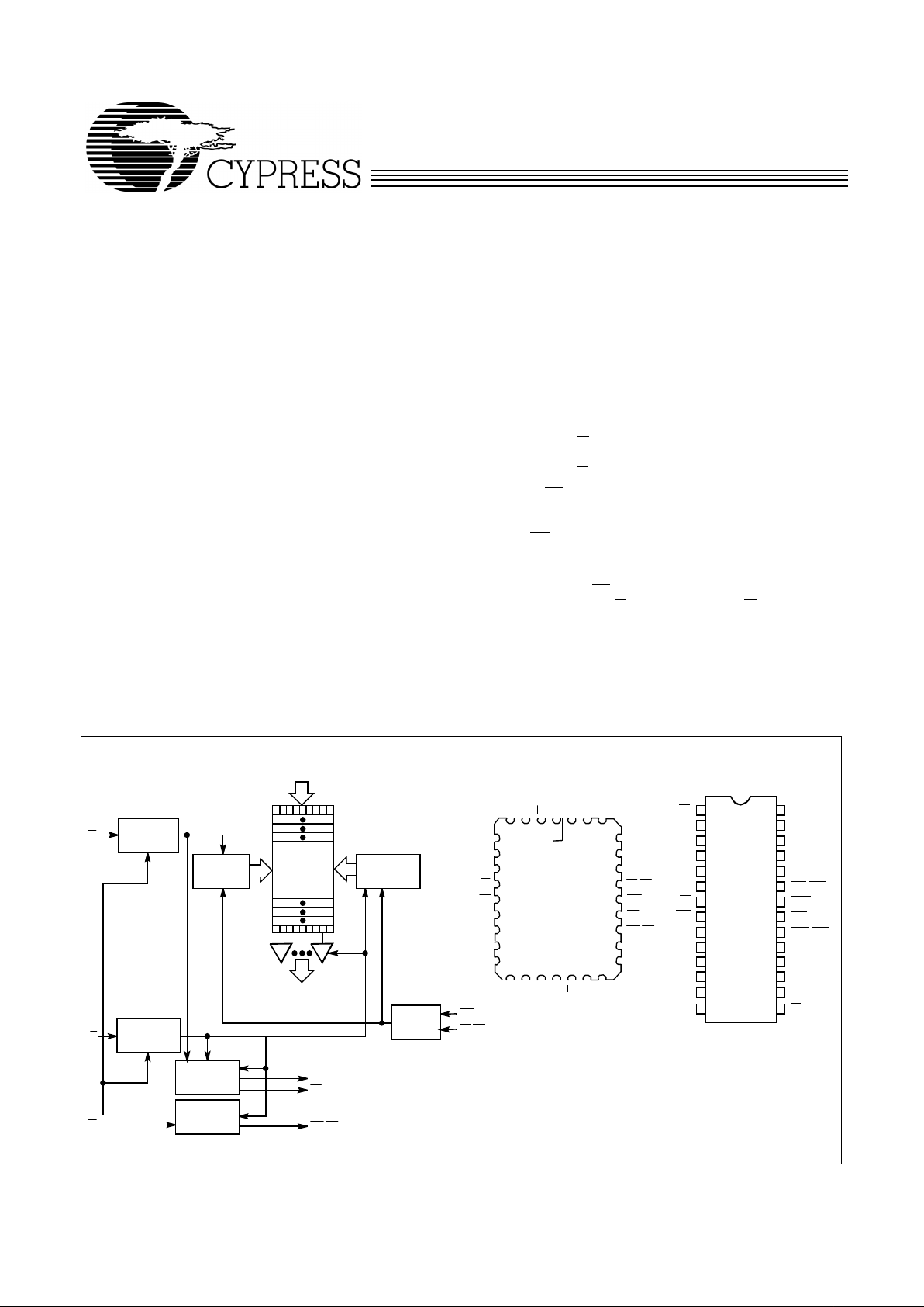
32K x
LogicBlock Diagram
Pin
Configurations
1
2
3
4
5
6
7
8
9
10
11
12
15
16
17
18
19
20
24
23
22
21
13
14
25
28
27
26
Top View
DIP
W
D
8
D
3
D
2
D
1
D
0
XI
FF
Q
0
Q
1
Q
2
GND
V
CC
D
4
FL/RT
MR
EF
XO/HF
Q
7
R
PLCC/LCC
Top View
Q
3
Q
8
D
5
D
6
D
7
Q
6
Q
5
Q
4
4 3 2 1 32 31 30
14 15 16 17 18 19 20
5
6
7
8
9
10
11
12
13
29
28
27
26
25
24
23
22
21
FL
/RT
MR
EF
XO/HF
Q
7
D
6
Q
6
D
7
NC
READ
CONTROL
WRITE
CONTROL
WRITE
POINTER
RESET
LOGIC
EXPANSION
LOGIC
RAM ARRAY
8K x 9
16K x 9
9
DATAINPUTS
(D
0
−
D8)
THREE–
STATE
BUFFERS
DATAOUTPUTS
(Q0-Q8)
W
READ
POINTER
FLAG
LOGIC
R
XI
EF
FF
XO/HF
MR
FL/RT
D
2
D
1
D
0
XI
FF
Q
0
Q
1
NC
Q
2
DDWNCVDD
3
8
cc45
Q
Q
GND
NC
R
Q
Q
3
8
4
5
C46XA–1
C46XA–2
C46XA–3
7C460A
7C462A
7C464A
7C460A
7C462A
7C464A
64K x 9
7C466A
7C466A
DUAL PORT
CY7C460A/CY7C462A
CY7C464A/CY7C466A
2
Maximum Ratings
(Above which the useful life may be impaired. F or user guidelines, not tested.)
Storage Temperature. .. ............. .. ............. .. .–65
°
C to +150°C
Ambient Temperature with
Power Applied.............................................–55
°
C to +125°C
Supply Voltage to Ground Potential...............–0.5V to +7.0V
DC V oltage Applied to Outputs
in High Z State............................................... –0.5V to +7.0V
DC Input Voltage............................................–0.5V to +7.0V
Power Dissipation ..........................................................1.0W
Output Current, into Outputs (LOW)............................20 mA
Static Discharge Voltage.................... .. ............. .. .. ....>2001V
(per MIL-STD-883, Method 3015)
Latch-Up Current.....................................................>200 mA
Selection Guide
7C460A-10
7C462A-10
7C464A-10
7C466A-10
7C460A-15
7C462A-15
7C464A-15
7C466A-15
7C460A-25
7C462A-25
7C464A-25
7C466A-25
Frequency (MHz) 50 40 28.5
Maximum Access Time (ns) 10 15 25
Operating Range
Range
Ambient
Temperature
V
CC
Commercial 0°C to + 70°C 5V ± 10%
Industrial –40°C to +85°C 5V ± 10%
Military
[1]
–55°C to +125°C 5V ± 10%
Electrical Characteristics
Over the Operating Range
[2]
Parameter Description Tes t Condi ti ons
7C460A/462A/464A/466A
(-10,-15,-25)
UnitMin. Max.
V
OH
Output HIGH Voltage VCC = Min., IOH = −2.0 mA 2.4 V
V
OL
Output LOW Voltage VCC = Min., IOL = 8.0 mA 0.4 V
V
IH
Input HIGH Voltage 2.2 V
CC
V
V
IL
Input LOW Voltage
−0.5
0.8 V
I
IX
Input Leakage Current GND < VI < V
CC
–10 +10
µA
I
OZ
Output Leakage Current R > VIH, GND < VO < V
CC
–10 +10
µA
I
CC
Operating Current VCC = Max.,
I
OUT
= 0 mA, Freq. = 20 MHz
60 mA
I
SB
Standby Current All Inpu ts = VIH min. 8 mA
Capacitance
[4]
Parameter Description Test Conditions Max. Unit
C
IN
Input Capacitance TA = 25°C, f = 1 MHz,
V
CC
= 4.5V
10 pF
C
OUT
Output Capacitance 12 pF
Notes:
1. T
A
is the “instant on” case temperature.
2. See the last page of this specification for Group A subgroup testing information.
3. For test purposes, not more than one output at a time should be shorted. Short circuit test duration should not exceed 1 second.
4. Tested initially and after any design or process changes that may affect these parameters.
CY7C460A/CY7C462A
CY7C464A/CY7C466A
3
AC Test Loads and Waveforms
3.0V
5V
OUTPUT
R1 500
Ω
R2
333
Ω
30pF
INCLUDING
JIG AND
SCOPE
GND
90%
10%
90%
10%
≤
5ns
≤
5
ns
5V
OUTPUT
R1 500
Ω
R2
333
Ω
5pF
INCLUDING
JIG AND
SCOPE
OUTPUT 2V
Equivalent to: THÉ VENIN EQUIVALENT
(b)
C460A–4
C460A–5
C460A–6
(a)
ALL INPUT PULSES
200
Ω
Switching Characteristics
Over the Operati ng Range
[2, 5]
Parameter Description
7C460A-10
7C462A-10
7C464A-10
7C466A-10
7C460A-15
7C462A-15
7C464A-15
7C466A-15
7C460A-25
7C462A-25
7C464A-25
7C466A-25
UnitMin. Max. Min. Max. Min. Max.
t
RC
Read Cycle Time 20 25 35 ns
t
A
Access Time 10 15 25 ns
t
RR
Read Recovery Time 10 10 10 ns
t
PR
Read Pulse Width 10 15 25 ns
t
LZR
Read LOW to Low Z 3 3 3 ns
t
DVR
[6]
Data Valid After Read HIGH 3 3 3 ns
t
HZR
[6]
Read HIGH to High Z 15 15 18 ns
t
WC
Write Cycle Time 20 25 35 ns
t
PW
Write Pulse Width 10 15 25 ns
t
HWZ
Write HIGH to Low Z 5 5 5 ns
t
WR
Write Recovery Time 10 10 10 ns
t
SD
Data Set-Up Time 9 9 9 ns
t
HD
Data Hold Time 0 0 0 ns
t
MRSC
MR Cycle Time 20 25 35 ns
t
PMR
MR Pulse Width 10 15 25 ns
t
RMR
MR Recovery Time 10 10 10 ns
t
RPW
Read HIGH to MR HIGH 10 15 25 ns
t
WPW
Write HIGH to MR HIGH 10 15 25 ns
t
RTC
Retransmit Cyc le Ti me 20 25 35 ns
t
PRT
Retransmit Pulse W idt h 10 15 25 ns
t
RTR
Retransmit Reco very Time 10 10 10 ns
t
EFL
MR to EF LOW 20 25 35 ns
t
HFH
MR to HF HIGH 20 25 35 ns
t
FFH
MR to FF HIGH 20 25 35 ns
t
REF
Read LOW to EF LOW 10 15 25 ns
t
RFF
Read HIGH to FF HIGH 10 15 25 ns
Notes:
5. Test conditions assume signal transmission time of 5 ns or less, timing reference levels of 1.5V and output loading of the specified I
OL/IOH
and 30-pF load
capacitance, as in part (a) of AC Test Loads, unless otherwise specified.
6. t
HZR
and t
DVR
use capacitance loading as in part (b) of AC Test Loads.
CY7C460A/CY7C462A
CY7C464A/CY7C466A
4
t
WEF
Write HIGH to EF HIGH 10 15 25 ns
t
WFF
Write LOW to FF LOW 10 15 25 ns
t
WHF
Write LOW to HF LOW 10 15 35 ns
t
RHF
Read HIGH to HF HIGH 10 15 35 ns
t
RAE
Effective Read from Write
HIGH
10 15 25 ns
t
RPE
Effective Rea d P ulse Wi dth
After EF
HIGH
10
15 25 ns
t
WAF
Effective Write from Read
HIGH
10 15 25 ns
t
WPF
Effective Write Pulse
Width After FF
HIGH
10
15 25 ns
t
XOL
Expansion Out LOW
Delay from Clock
10 15 25 ns
t
XOH
Expansion Out HIGH
Delay from Clock
10 15 25 ns
Switching Characteristics
Over the Operati ng Range
[2, 5]
(continued)
Parameter Description
7C460A-10
7C462A-10
7C464A-10
7C466A-10
7C460A-15
7C462A-15
7C464A-15
7C466A-15
7C460A-25
7C462A-25
7C464A-25
7C466A-25
UnitMin. Max. Min. Max. Min. Max.

CY7C460A/CY7C462A
CY7C464A/CY7C466A
5
Switching Waveforms
[7]
Notes:
7. A HIGH-to-LOW transition of either the write or read strobe causes a HIGH-to-LOW transition of the responding flag. Correspondingly, a LOW- to-HIGH strobe
transition causes a LOW-to-HIGH flag transition.
8. W
and R = VIH around the rising edge of MR.
9. t
MSRC
= t
PMR
+ t
RMR
Asynchronous Read and Write
C460A–7
DATA VALIDDATA VALID
DATA VALID DATA VALID
t
SD
t
HD
t
RC
t
PR
t
A
t
RR
t
A
t
LZR
t
DVR
t
HZR
t
WC
t
PW
t
WR
R
Q
0
−
Q
8
W
D
0
−
D
8
t
SD
t
HD
t
PW
Master Reset
MR
R,W
HF
FF
EF
t
MRSC
t
PMR
t
EFL
t
HFH
t
FFH
t
RPW
t
WPW
t
RMR
C460A–8
[9]
[8]
HALF FULL+1HALF FULL HALF FULL
W
R
HF
t
WHF
t
RHF
HalfFullFlag
C460A–9

CY7C460A/CY7C462A
CY7C464A/CY7C466A
6
Notes:
10. t
RTC
= t
PRT
+ t
RTR
.
11. EF
, HF , and FF may change state during retransmit as a result of the offset of the read and write pointers, but flags will be valid at t
RTC
, except for the CY7C46x-20
(Military), whose flags will be valid after t
RTC
+ 10 ns.
Switching Waveforms
[7]
(continued)
Last WritetoFirst ReadFullFlag
C460A–10
LAST WRITE FIRST READ
ADDITIONAL
READS FIRST WRITE
t
WFF
t
RFF
R
W
FF
Last READ to First WRITE Empty Flag
C460A–11
VALID
LAST READ FIRST WRITE
ADDITIONAL
WRITES
FIRST READ
VALID
t
REF
t
WEF
t
A
W
R
EF
DATA OUT
Retransmit
C460A–12
t
RTC
t
PRT
t
RTR
FL/RT
R,W
t
RTC
t
RTR
[10,11]

CY7C460A/CY7C462A
CY7C464A/CY7C466A
7
Switching Waveforms
[7]
(continued)
Full Flag and WriteData Flow-Through M ode
C460A–13
R
W
FF
DATA IN
DATA
OUT
DATA VALID
DATA VALID
t
WAF
t
WPF
t
WFF
t
RFF
t
SD
t
HD
t
A
EmptyFlagand Read Data Flow-Through Mode
C460A–14
W
R
EF
DATA IN
DATA
OUT
DATA VALID
t
RAE
t
REF
t
WEF
t
HWZ
t
A
t
RPE

CY7C460A/CY7C462A
CY7C464A/CY7C466A
8
Architecture
Resetting the FIFO
Upon power-up, the FIFO must be reset with a master reset
(MR
) cycle. This ca uses the FI FO t o enter the em pty condit io n
signified by the Empty flag (EF
) being LOW, and both the Half
Full (HF
), and Full flags (FF) being HIGH. Read (R) and Write
(W
) must be HIGH t
RPW/tWPW
before and t
RMR
after the rising
edge of MR
for a valid reset cycle. If reading from the FIFO
after a reset cycle is attempted, the outputs will all be in the
high-impedance state.
Writing Data to the FIFO
The avail abil ity of at least one empty locat ion is indica ted by a
HIGH FF
. The falling edge of W initiates a write cycle. Data
appearing at the inputs (D
0−D8
) tSD before and tHD after the
rising edge of W
will be stored sequent ial ly in the FIFO.
The EF
LOW-to-HIGH transition occurs t
WEF
after the first
LOW-to-HIGH transition of W
for an empty FIFO. HF goes
LOW t
WHF
after the falling edge of W following the FIFO actu-
ally being half full. Therefore, the HF
is active once the FIFO
is filled t o half its capacity plus one word. HF
will remain LOW
while less than one half of t otal memory is avai lable f or writing.
The LOW -to- HIGH tran siti on of HF
occurs t
RHF
after the rising
edge of R
when the FIFO goes from half full +1 to half full. HF
is available in standalone and width expansion modes. FF
goes LOW t
WFF
after the falling edge of W, during the cycle in
which the last av ailab le locat ion is fill ed. Internal l ogic pre vents
overrunning a full FIFO. Writes to a full FIFO are ignored and
the write pointer is not incremented. FF
goes HIGH t
RFF
after
a read from a full FIFO.
Reading Data from the FIFO
The falling e dge of R
initiates a re ad cycle if the EF is not LO W .
Data outputs (Q
0−Q8
) are in a high-impedance condition be-
tween read operations (R
HIGH), when the FIFO is empty, or
when the FIFO is not the active de vice in the depth e xpa nsion
mode.
When one word is in t he FIFO, the f alling edge of R
initiates a
HIGH-to-LOW transition of EF
. When the FIFO is empty, the
outputs are in a high-impedance state. Reads to an empty
FIFO are ignored and do no t incr ement the r ead point er . F rom
the empty condition, the FIFO can be read t
WEF
after a valid
write.
Retransmit
The retransmit feature is beneficial when transferring packets
of data. It enables the receipt of data to be acknowledged by
the receiver and retransmitted if necessary. The retransmit
(RT
) input is active in the standalone and width expansion
modes. The retransm it feat ure is intended f or u se when a num-
Note:
12. Expansion out of device 1 (XO
1
) is connected to expansion in of device 2 (XI2).
Switching Waveforms
[7]
(continued)
Expansion TimingDiagrams
C460A–15
R
W
XO1(XI2)
D
0
−
D
8
DATA VALID
DATA DATA
VALID
VALID
t
XOL
t
HD
t
SD
t
SD
t
HD
t
XOL
t
LZR
t
A
t
DVR
t
A
t
DVR
t
HZR
XO1(XI2)
Q
0
−
Q
8
C460A–16
t
WR
t
RR
DATA VALID
t
XOH
t
XOH
[12]
[12]

CY7C460A/CY7C462A
CY7C464A/CY7C466A
9
ber of writes equal -to-or-less-than the depth of the FIFO have
occurred since the last MR
cycle. A LOW pulse on RT resets
the internal read pointer to the first physical location of the
FIFO. R
and W must both be HIGH while and t
RTR
after re transmit is LOW. With ev ery read cycle after retrans mit, previously accessed data is read an d the read poin ter in creme nted
until equal to the write pointer . Full, Half Full, and Em pty flags
are governed by the relative locations of the read and write
pointers and are updated during a retr ansmit cycle. Data written to the FIFO after act ivation of RT
are transmitted also.
The full depth of the FI FO can be repeatedly retransmitted.
Standalone/Width Expansion Modes
Standalone and wid th expansion modes are se t by grounding
expans ion in (XI
) and tying fi rst load (FL) to VCC prior to a MR
cycle. FI FOs can b e expa nded in wi dth to pr o vide wor d widths
greater than nine in increments of nine. During width expansion mode, all control line inputs are common to all devices,
and flag outputs from any device can be monitored.
Depth Expansion Mode (
see Figure 1
)
Depth expansion mode is entered when, during a MR
cycle,
expansion out (XO
) of one device is connected to expansion
in (X I
) of the nex t de vice, with XO of t he last devi ce con nected
to XI
of the first device. In the depth expansion mode, th e first
load (FL
) input, when grounded, indicates that this is the first
part to be loaded. All other devices must have this pin HIGH.
To enable the correct FIFO, XO
is pulsed LOW when the last
physical location of the previous FIFO is written to and is
pulsed LO W again wh en the last p hysica l locat ion is read. Onl y
one FIFO is enabled for Read and one is enabled for Write at
any given time. All other devices are in standby.
FIFOs can also be expanded simultaneously in depth and
width. Consequently, any depth or width FIFO can be created
with word widths in increments of nine. When expanding in
depth, a composite FF
is created by ORing the FFs together.
Likewise, a composite EF
is created by ORing EFs together.
HF
and RT functions are not available in depth expansion
mode.
Figure 1. Depth Expansion
CY7C460A
CY7C462A
CY7C464A
W
RS
XI
FL
EF
XO
FF
XI
FL
EF
XO
XI
FL
EF
XO
FF
R
EMPTY
FULL
D
0-8
Q
0-8
9
9
9
9
9
FF
V
CC
* FIRSTDEVICE
*
C460A–17
CY7C460A
CY7C462A
CY7C464A
CY7C460A
CY7C462A
CY7C464A
CY7C466A
CY7C466A
CY7C466A

CY7C460A/CY7C462A
CY7C464A/CY7C466A
10
Ordering Information
8K x 9 Asynchronous FIFO
Speed
(ns) Ordering Code
Package
Name Package Type
Operating
Range
10 CY7C460A-10JC J65 32-Lead Plastic Leaded Chip Carrier Commercial
CY7C460A-10PC P15 28-Lead (600-M il ) Molded DIP
CY7C460A-10PTC P21 28- Lead (300-Mil) Molded DIP
CY7C460A-10JI J65 32-Lead Plastic Leaded Chip Carrier Industrial
15 CY7C460A-15JC J65 32-Lead Plastic Leaded Chip Carrier Commercial
CY7C460A-15PC P15 28-Lead (600-M il ) Molded DIP
CY7C460A-15PTC P21 28- Lead (300-Mil) Molded DIP
25 CY7C460A-25JC J65 32-Lead Plastic Leaded Chip Carrier Commercial
CY7C460A-25PC P15 28-Lead (600-M il ) Molded DIP
CY7C460A-25PTC P21 28- Lead (300-Mil) Molded DIP
16K x 9 Asynchronous FIFO
Speed
(ns)
Ordering Code
Package
Name
Package Type
Operating
Range
10 CY7C462A-10JC J65 32-Lead Plastic Leaded Chip Carrier Commercial
CY7C462A-10PC P15 28-Lead (600-Mil) Molded DIP
CY7C462A-10PTC P21 28-Lead (300-Mil) Molded DIP
CY7C462A-10JI J65 32-Lead Plastic Leaded Chip Carrier Industrial
15 CY7C462A-15JC J65 32-Lead Plastic Leaded Chip Carrier Commercial
CY7C462A-15PC P15 28-Lead (600-Mil) Molded DIP
CY7C462A-15PTC P21 28-Lead (300-Mil) Molded DIP
25 CY7C462A-25JC J65 32-Lead Plastic Leaded Chip Carrier Commercial
CY7C462A-25PC P15 28-Lead (600-Mil) Molded DIP
CY7C462A-25PTC P21 28-Lead (300-Mil) Molded DIP
32K x 9 Asynchronous FIFO
Speed
(ns) Ordering Code
Package
Name Package Type
Operating
Range
10 CY7C464A-10JC J65 32-Lead Plastic Leaded Chip Carrier Commercial
CY7C464A-10PC P15 28-Lead (600-Mil) Molded DIP
CY7C464A-10PTC P21 28-Lead (300-Mil) Molded DIP
CY7C464A-10JI J65 32-Lead Plastic Leaded Chip Carrier Industrial
15 CY7C464A-15JC J65 32-Lead Plastic Leaded Chip Carrier Commercial
CY7C464A-15PC P15 28-Lead (600-Mil) Molded DIP
CY7C464A-15PTC P21 28-Lead (300-Mil) Molded DIP
CY7C464A-15LMB L55 32-Pin Rectangular Leadless Chip Carrier Military
25 CY7C464A-25JC J65 32-Lead Plastic Leaded Chip Carrier Commercial
CY7C464A-25PC P15 28-Lead (600-Mil) Molded DIP
CY7C464A-25PTC P21 28-Lead (300-Mil) Molded DIP

CY7C460A/CY7C462A
CY7C464A/CY7C466A
11
Ordering Information
(continued)
64K x 9 Asynchronous FIFO
Speed
(ns) Orderi ng Code
Package
Name Package Type
Operating
Range
10 CY7C466A-10JC J65 32-Lead Plastic Leaded Chip Carrier Commercial
CY7C466A-10PC P15 28-Lead (600-Mil) Molded DIP
CY7C466A-10PTC P21 28-Lead (300-Mil) Molded DIP
CY7C466A-10JI J65 32-Lead Plastic Leaded Chip Carrier Industrial
15 CY7C466A-15JC J65 32-Lead Plastic Leaded Chip Carrier Commercial
CY7C466A-15PC P15 28-Lead (600-Mil) Molded DIP
CY7C466A-15PTC P21 28-Lead (300-Mil) Molded DIP
CY7C466A-15LMB L55 32-Pin Rectangular Lea dless Chip Carrier Military
25 CY7C466A-25JC J65 32-Lead Plastic Leaded Chip Carrier Commercial
CY7C466A-25PC P15 28-Lead (600-Mil) Molded DIP
CY7C466A-25PTC P21 28-Lead (300-Mil) Molded DIP

CY7C460A/CY7C462A
CY7C464A/CY7C466A
12
MILI TARY SPECIF ICATION S
Group A Subgroup Testing
Document #: 38-00627-A
DC Characteristics
Parameter Subgroups
V
OH
1, 2, 3
V
OL
1, 2, 3
V
IH
1, 2, 3
VIL Max. 1, 2, 3
I
IX
1, 2, 3
I
CC
1, 2, 3
I
SB1
1, 2, 3
I
SB2
1, 2, 3
I
OS
1, 2, 3
I
OZ
1, 2, 3
Switching Characteristics
Parameter Subgroups
t
RC
9, 10, 11
t
A
9, 10, 11
t
RR
9, 10, 11
t
PR
9, 10, 11
t
LZR
9, 10, 11
t
DVR
9, 10, 11
t
HZR
9, 10, 11
t
WC
9, 10, 11
t
PW
9, 10, 11
t
HWZ
9, 10, 11
t
WR
9, 10, 11
t
SD
9, 10, 11
t
HD
9, 10, 11
t
MRSC
9, 10, 11
t
PMR
9, 10, 11
t
RMR
9, 10, 11
t
RPW
9, 10, 11
t
WPW
9, 10, 11
t
RTC
9, 10, 11
t
PRT
9, 10, 11
t
RTR
9, 10, 11
t
EFL
9, 10, 11
t
HFH
9, 10, 11
t
FFH
9, 10, 11
t
REF
9, 10, 11
t
RFF
9, 10, 11
t
WEF
9, 10, 11
t
WFF
9, 10, 11
t
WHF
9, 10, 11
t
RHF
9, 10, 11
t
RAE
9, 10, 11
t
RPE
9, 10, 11
t
WAF
9, 10, 11
t
WPF
9, 10, 11
t
XOL
9, 10, 11
t
XOH
9, 10, 11

CY7C460A/CY7C462A
CY7C464A/CY7C466A
13
Package Diagrams
32-Lead Plastic Leaded Chip Carrier J65
51-85002-B
32-Pin Rectangular Leadless Chip Carrier L55
MIL-STD-1835 C-12
51-80068

CY7C460A/CY7C462A
CY7C464A/CY7C466A
© Cypress Semiconductor Corporation, 1999. The information contained herein is subject to change without notice. Cypress Semiconductor Corporation assumes no responsibility for the use
of any circuitry other than circuitry embodied in a Cypress Semiconductor product. Nor does it con vey or imply any license under patent or other rights. Cypress Semiconductor does not authorize
its products for use as critical components in life-support systems where a malfunction or failure may reasonably be expected to result in significant injury to the user. The inclusion of Cypress
Semiconductor products in life-support systems application implies that the manufacturer assumes all risk of such use and in doing so indemnifies Cypress Semiconductor against all charges.
Package Diagrams
(continued)
51-85017-A
28-Lead(600-Mil) MoldedDIPP15
51-85014-B
28-Lead(300-Mil) MoldedDIPP21
 Loading...