

Page 1

LTT1450G
Ku-Band Loop Test Translator
Installation and Operation Manual
TM063 - Rev. 1
February, 1997
- NOTICE -
1997, Radyne Corporation. All rights reserved. Unauthorized
reproduction of this manual in any form without the expressed
written approval of Radyne Corporation is strictly prohibited.
This manual may not in whole or in part be copied, reproduced,
translated or reduced to any electronic or magnetic storage
medium without the written consent of a duly authorized officer
of Radyne Corporation.
Radyne Corporation • 5225 South 37th St. • Phoenix, AZ 85040 • (602) 437-9620 • Fax: (602) 437-4811
Page 2

Page 3

LTT1450G Ku-Band Loop Test Translator Warranty Policy
RADYNE WARRANTY POLICY
WARRANTY AND SERVICE
Radyne (Seller) warrants the items manufactured and sold by Radyne to be free of defects in material
and workmanship for a period of two (2) years from date of shipment Radyne's obligation under its
warranty is limited in accordance with the periods of time and all other conditions stated in all
provisions of this warranty.
This warranty applies only to defects in material and workmanship in products manufactured by
Radyne. Radyne makes no warranty whatsoever concerning products or accessories not of its
manufacture.
Repair, or at Radyne's option, replacement of the Radyne products or defective parts therein shall be
the sole and exclusive remedy for all valid warranty claims.
WARRANTY PERIOD
The applicable warranty period shall commence on the date of shipment from Radyne's facility to the
original purchaser and extend for the stated period following the date of shipment. Upon beginning of
the applicable Radyne warranty period, all customer's remedies shall be governed by the terms stated
or referenced in this warranty. In-warranty repaired or replacement products or parts are warranted
only for the remaining unexpired portion of the original warranty period applicable to the repaired or
replaced products or parts. Repair or replacement of products or parts under warranty does not
extend the original warranty period.
WARRANTY COVERAGE LIMITATIONS
The following are expressly not covered under warranty:
1. Any loss, damage and/or malfunction relating in any way to shipping, storage, accident, abuse,
alteration, misuse, neglect, failure to use products under normal operating conditions, failure to use
products according to any operating instructions provided by Radyne, lack of routine care and
maintenance as indicated in any operating maintenance instructions, or failure to use or take any
proper precautions under the circumstances.
2. Products, items, parts, accessories, subassemblies, or components which are expendable in
normal use or are of limited life, such as but not limited to, bulbs, fuses, lamps, glassware, etc.
Radyne reserves the right to revise the foregoing list of what is covered under this warranty.
WARRANTY REPLACEMENT AND ADJUSTMENT
Radyne will not make warranty adjustments for failures of products or parts which occur after the
specified maximum adjustment period. Unless otherwise agreed, failure shall be deemed to have
occurred no more than seven (7) working days before the first date on which a notice of failure is
received by Radyne. Under no circumstances shall any warranty exceed the period stated above
unless expressly agreed to in writing by Radyne.
TM063 - Rev. 1 ii
Page 4

Warranty Policy LTT1450G Ku-Band Loop Test Translator
LIABILITY LIMITATIONS
This warranty is expressly in lieu of and excludes all other express and implied warranties, including
but not limited to warranties of merchantability and of fitness for particular purpose, use, or
applications, and all other obligations or liabilities on the part of Radyne, unless such other warranties,
obligations, or liabilities are expressly agreed to in writing by Radyne.
All obligations of Radyne under this warranty shall cease in the event its products or parts thereof
have been subjected to accident, abuse, alteration, misuse or neglect, or which have not been
operated and maintained in accordance with proper operating instructions.
IN NO EVENT SHALL RADYNE BE LIABLE FOR INCIDENTAL, CONSEQUENTIAL, SPECIAL OR
RESULTING LOSS OR DAMAGE OF ANY KIND HOWSOEVER CAUSED. RADYNE’S LIABILITY
FOR DAMAGES SHALL NOT EXCEED THE PAYMENT, IF ANY, RECEIVED BY RADYNE FOR
THE UNIT OR PRODUCT OR SERVICE FURNISHED OR TO BE FURNISHED, AS THE CASE MAY
BE, WHICH IS THE SUBJECT OF CLAIM OR DISPUTE.
Statements made by any person, including representatives of Radyne, which are inconsistent or in
conflict with the terms of this warranty, shall not be binding upon Radyne unless reduced to writing
and approved by an officer of Radyne.
WARRANTY REPAIR RETURN PROCEDURE
Before a warranty repair can be accomplished, a Repair Authorization must be received. It is at this
time that Radyne will authorize the product or part be returned to the Radyne facility or if field repair
will be accomplished. The Repair Authorization may be requested in writing or by telephoning:
Radyne Corporation
5225 South 37th Street
Phoenix, Arizona 85040 (USA)
ATTN: Customer Support
Phone: (602) 437-9620 Fax: (602) 437-4811
Any product returned to Radyne for examination must be sent prepaid via the means of transportation
indicated as acceptable to Radyne. Return Authorization Number must be clearly marked on the
shipping label. Returned products or parts should be carefully packaged in the original container, if
possible, and unless otherwise indicated, shipped to the above address.
NON-WARRANTY REPAIR
When a product is returned for any reason, Customer and its shipping agency shall be responsible for
all damage resulting from improper packing and handling, and for loss in transit, not withstanding any
defect or nonconformity in the product. By returning a product, the owner grants Radyne permission
to open and disassemble the product as required for evaluation. In all cases, Radyne has sole
responsibility for determining the cause and nature of failure, and Radyne's determination with regard
thereto shall be final.
TM063 - Rev. 1 iii
Page 5

Page 6
LTT1450G Ku-Band Loop Test Translator Record of Revisions
LTT1450G Ku-Band Loop Test Translator
Installation and Operation Manual
TM063 - Record of Revisions
Radyne Corporation is constantly improving its products and therefore the information in this document is
subject to change without prior notice. Radyne Corporation makes no warranty of any kind with regard to
this material, including but not limited to the implied warranties of merchantability and fitness for a
particular purpose. No responsibility for any errors or omissions that may pertain to the material herein is
assumed. Radyne Corporation makes no commitment to update nor to keep current the information
contained in this document. Radyne Corporation assumes no responsibility for use of any circuitry other
than the circuitry employed in Radyne Corporation’s systems and equipment.
Revision
Level
Date Reason for Change
1 2-24-97 Initial Release
TM063 - Rev. 1 iv
Page 7

LTT1450G Ku-Band Loop Test Translator Table of Contents
Table of Contents
1.0 Introduction…..………………………………………………………………………………………… 1-1
1.1 Model LTT1450G Ku-Band Translator Overview………………………………………………….. 1-1
2.0 Installation Requirements…..…...…………………………………………………………………… 2-1
2.1 Mounting….………..…………………………………………………………………………………… 2-1
2.2 Power-Up…..…………….…..………………………………………………………………………… 2-1
2.3 Apply Signals..…………………………………………………………………………………………. 2-2
2.4 Receive Signal Injection.….…………………………………………………………………………2-2
2.5 Hardware Description………………………………………………………………………………… 2-2
2.5.1 Ku-Band PLO….……………………………………………………………………………………2-3
2.5.2 Ku-Band Converter Module..……..……………………………………………………………… 2-3
2.5.3 Microcontroller PWB AS/1030…………………………………………………………….. 2-4
3.0 Operating Procedures ..……………..….……………………………………………………………. 3-1
3.1 Operator Controls……..……..……………………………………………………………………… 3-1
3.1.1 Power On/Off……………………………………………………………………………………… 3-1
3.1.2 Power LED…………………………………………………………………………………………… 3-1
3.1.3 FREQ ADJ.………………………………………………………………………………………… 3-1
3.1.4 RCV Monitor………………………………………………………………………………………… 3-1
3.1.5 EXT Reference LED………………………………………………………………………………… 3-1
3.1.6 Remote LED………………………………………………………………………………………… 3-2
3.1.7 LO Fault..……………………………………………………………………………………………3-2
3.1.8 LCD Display…………………………………………………………………………………………3-2
3.2 Pushbutton Panel.…………………………………………………………………………………… 3-2
3.3 Rear Panel Connectors and Adjustments……………………………………………………………3-3
3.3.1 TX and RX RF I/O………………………………………………………………………………….. 3-3
3.3.2 REF IN……………………………………………………………………………………………… 3-3
TM063 - Rev. 1 v
Page 8

LTT1450G Ku-Band Loop Test Translator Table of Contents
3.3.3 REF OUT…………………………………………………………………………………………… 3-3
3.3.4 Test Fault (J5)………………………………………………………………………………………3-3
3.3.5 Serial Port (J6)……………………………………………………………………………………… 3-4
3.3.6 GND………………………………………………………………………………………………… 3-5
3.3.7 100/240 Vac Power Entry Module………………………………………………………………… 3-5
4.0 Confidence Test and Troubleshooting……………………………………………………………… 4-1
4.1 Confidence Test Procedure………………………………………………………………………… 4-1
4.1.1 Power ON Testing……….………………………………………………………………………… 4-1
4.1.2 Transfer Characteristics Testing….……………………………………………………………… 4-1
4.1.3 Attenuator Calibration Testing.…..…….……………………………………………………………4-2
4.1.4 Spectral Response Testing……..…………………………………………………………………4-2
4.2 Troubleshooting....……………………………………………………………………………………4-2
4.2.1 LO Fault….……….…………………………………………………………………………………4-2
4.2.2 Transfer Characteristics Faults…..……………………………………………………………… 4-3
4.3 Attenuator DAC and Calibration...…..………………………………………………………………4-3
5.1 Introduction……………..…..………………………………………………………………….………. 5-1
5.2 Command Structure………………………………………………………………………………… 5-1
5.2.1 Status Prompt....……………………………………………………………………………………5-1
5.2.2 Control Commands…...……………………………………………………………………………5-2
5.3 Status Commands..…..………………………………………………………………………………5-3
5.4 Calibration Commands…..…………………………………………………………………………… 5-4
5.4.1 Set-Calibrate-Mode Command.…………………………………………………………………… 5-4
5.4.2 Valid Commands while in CAL Mode…..………………………………………………………… 5-4
Appendix A - Technical Specifications..……………………………………………………………… A-1
Appendix B - Configuration Drawings…………………………………………………………………... B-1
TM063 - Rev. 1
vi
Page 9

LTT1450G Ku-Band Loop Test Translator Table of Contents
TM063 - Rev. 1
vii
Page 10

Page 11
LTT1450G Ku-Band Loop Test Translator Description
Section One - LTT1450G
Ku-Band Loopback Test Translator Description
1.0 Introduction
This manual is designed to serve as a guide during installation, operation, and interfacing of the Model
LTT1450G Ku-Band Loopback Test Translator. This manual describes operation of the microwave,
analog, and digital circuitry found in the translator. This dialogue is offered to provide insight into the
normal operation of the system as well as to provide assistance in identifying a faulty subsystem. The
level of description in this manual is not intended to provide information for component level test or
alignment. These functions are best performed by trained factory technicians.
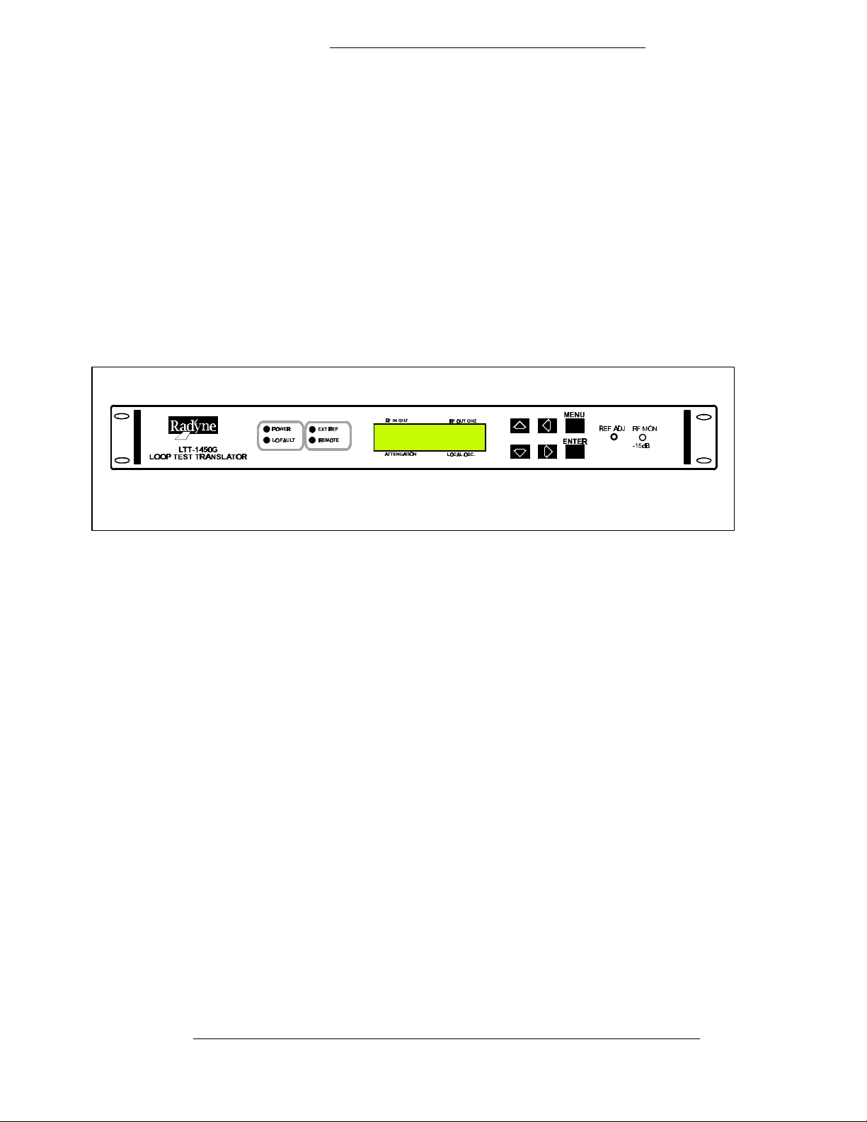
Figure 1-1. LTT1450G Front Panel
1.1 Model LTT1450G Ku-Band Translator Overview
The Model LTT1450G Global Ku-band Loopback Test Translator is designed to provide frequency
conversion of Ku-Band earth terminal uplink transmit carrier signals to earth terminal downlink receive
carrier signals for the purpose of testing all of the transmit and receive hardware simultaneously in the
earth terminal prior to acquiring actual satellite transponder space. Digital information to the MODEM
equipment will be received where it can be compared to that which was transmitted for the purpose of
determining a precise bit error rate. This function is normally provided by a bit error rate monitor (BER
Tester).
The LTT1450G translator is capable of converting Ku-Band uplink signals in the uplink 500 MHz band.
Uplink signals from either the output of the upconverter or HPA in the frequency range of 14.0 to 14.5
GHz are translated in four user-selectable 500 MHz bands covering the downlink frequency range of
10.95 to 12.70 GHz.
Output signal gain is variable in 0.1 dB increments via the front panel pushbuttons or serial remote
control. A PIN diode attenuator provides voltage controlled attenuation of the output signals in one dB
steps over the range of 00 to 60 dB. The serial port allows remote control of attenuation in precise 0.1dB
steps.
The local oscillator used in the translator is a four-band high-Q oscillator, phase locked to a 25 MHz
intermediate frequency crystal oscillator. The 25 MHz crystal oscillator is in turn locked to either an
internal 10.000 MHz ovenized SC-cut 3rd overtone crystal oscillator or to an external 5 or 10 MHz
external reference. The dual loop architecture used in the PLOs provide for a typical 14 dB
improvement over 20 Log N. In this way, the phase noise of the local oscillators is independent of the
phase noise of the internal or external 5 or 10 MHz references.
TM063 - Rev. 1 Page 1-1
Page 12

Description LTT1450G Ku-Band Loop Test Translator
The use of an external reference allows the translation to be phase coherent with the external reference.
The frequency of translation will track the frequency of the external reference to approximately 200 KHz
at the output frequency. This allows the external reference to contain Doppler information.
Page 1-2 TM063 - Rev. 1
Page 13

LTT1450G Ku-Band Loop Test Translator Installation
Section 2 - Installation
2.0 Installation Requirements
2.1 Mounting
The Radyne Loopback Test Translator product line is designed for either a rack mount installation or
bench top use. Rack mounting the test translator can be accomplished by securing the chassis front
panel with standard rack mount hardware. The welded construction of the test translator chassis makes
this a secure method of installation. Alternately, the chassis is equipped to accept standard rack
mounting slides if so desired. In a permanent rack installation, the adhesive rubber feet on the underside
of the chassis are intended to be removed if they interfere with other equipment. Ventilation of the
chassis is via side vents, so stacking the test translator with other chassis’ does not pose a problem. It is
assumed however, that the ambient temperatures in the rack will be maintained to less than 50 degrees
Celsius.
2.2 Power-up
Primary power may be applied via the AC line receptacle. Unless indicated otherwise, the test translator
may be operated from 100 to 240 volts AC at 50 to 60 Hertz. Turn the power switch on the Power Entry
Module at the rear panel to the ON position. At this time, the green power LED will illuminate and the
red LO fault will also illuminate momentarily. Note that if the test translator is being powered up from a
cold start, the momentary LO fault may last for a few minutes and should clear after the internal
ovenized reference oscillator stabilizes on frequency. It is not uncommon for the cold ovenized oscillator
to be off by as much a hundred hertz. Once stabilized (20 minutes), the ovenized oscillator will be
accurate to better than ±0.005 ppm. The test translators are designed for continuous operation. The
units draw little power (less than 20 watts) and may be left powered-up indefinitely.
Shielded cables with the shield terminated to conductive backshells are required in order to meet EMC
directives.
Cables with insulation flammability ratings of 94V0 or better are required in order to meet low voltage
directives.
2.3 Apply Signals
Apply the transmit signal to the TX RF input port in the good operating range of -5 dBm to - 25 dBm.
Good operating range is defined as signal levels that will guarantee a linear response with low
intermodulation and spurious content. An input level of -10 dBm is considered to be ideal. If multiple
carriers are to be translated simultaneously, it is recommended that the total power not be greater than -5
dBm for the same reasons. The test translator can be interfaced directly with most upconverter outputs.
When interfaced to an SSPA or TWTA, attenuator pads and/or directional couplers may be used to
attenuate the power of the signal to a good operating range.
Signal type may be CW or modulated for set-up. A CW signal has some advantages for use in testing
integrity of the hardware to be looped back. Naturally, a CW signal could never be used to check the
performance of the transmit and receive hardware over a satellite. But, with the test translator, a CW
signal can be used to test the stability and phase noise of the synthesizers in the up and downconverters.
Test translator phase noise is typically 20 dB better than most synthesized converters and as such
should never contribute to any noise appearing close to the carrier.
TM063 - Rev. 1 Page 2-1
Page 14

Installation LTT1450G Ku-Band Loop Test Translator
2.4 Receive Signal Injection
The translated receive signal is available at the RX signal output port. This signal will be the transmit
input signal translated by the LO frequency represented mathematically as TX-LO=RX. With the
attenuator set to 00, the Rx signal will be 15 dB lower in power.
Alternately, the RX signal can be viewed on a spectrum analyzer with an additional 15 dB of attenuation
at the Rx monitor SMA connector on the front panel.
Next, you will want to set the power level of the receive signal for injection into the receive hardware. To
inject the signal directly into a downconverter, a small amount of additional attenuation may be required.
Typical downconverter input saturations may run as high as -35 dBm. With a TX input level of -10 dBm
and 20 dB of attenuation, an output of -45 dBm can be attained. This will allow direct interface with the
downconverter.
If you wish to include an LNA in the receive path, additional attenuation of 50 to 70 dB will be required.
Using an LNA in the receive path is an excellent method of raising the noise floor of the receive signal
without having to inject external broadband noise. In order to test the BER performance of a system, it
becomes necessary to degrade the signal-to-noise ratio of the receive signal to a range of 5 to 15 dB
Eb/No. The noise figure of the LNA will guarantee that when the receive signal, when attenuated to
within 5 to 15 dB, the noise floor (No) of the LNA will yield a usable signal-to-noise ratio.
Please note that as a rule, the output of the translator should be attenuated to reach the desired power
level.
NOTE: Always attenuate the RX output path versus attenuating the TX input signal beyond -25
dBm to achieve the desired signal power.
2.5 Hardware Description
The Model LTT1450G Translator is comprised of a phase-locked oscillator source and a converter
module. The phase-locked oscillator subsystem provides the local oscillator frequencies for the converter
module. The converter module is a complete microwave integrated assembly that contains the filters,
mixer, amplifier and voltage-controlled attenuator.
The microcontroller module (AS1030) is an 8-bit Intel 80C32 microprocessor-based subsystem. The
controller contains various power supplies that provide positive and negative voltages used throughout
the translator, a 12-bit digital-to-analog converter, an 8-channel, 8-bit analog-to-digital converter, 24 bits
of parallel input and output, and a serial interface.
The A/D allows monitoring of various phase-lock loop voltages throughout the system. The 12-bit D/A
provides the precise currents for attenuation control. A nonvolatile RAM on the microcontroller board
stores calibration data for the different look-up tables. The parallel I/O provides the interface to the front
panel and to the LO selector module.
A 10.000 MHz ovenized oscillator assembly located at the rear of the chassis provides the internal
reference to each of the phase lock oscillator modules. This assembly also provides an interface for
external references to be applied to the system. An external reference, when applied to the system, is
exclusively OR’d with the internal 10.0 MHz oscillator. The microcontroller will detect the presence of an
external reference and will turn the internal reference off.
Page 2-2 TM063 - Rev. 1
Page 15

LTT1450G Ku-Band Loop Test Translator Installation
A single 15 Vdc, 25-watt power supply provides the current to run the translator. The system is designed
to minimize power consumption.
The following section provides a description of the various signals that are present on each assembly:
2.5.1 Ku-Band PLO
The Ku-Band PLO (AS/5003B) is a Four-Band, Microstrip dual-loop phase-locked oscillator. The
primary loop of the PLO runs at either 1.75, 2.30, 2.55, or 3.05 GHz with a 25 MHz internal reference.
Signals in and out of the PLO include the following:
5.0 MHz Ref In
A 5.0 MHz reference is routed into the PLO module via this SMB connector. This signal is a
CMOS level.
+15 Vdc - This pin is the primary power input pin to the PLO module.
VT25-C
The VT25-C signal is the phase lock loop voltage from the 25 MHz phase-lock loop in the PLO.
The PLO contains a 25 MHz VCXO that drives the sampling phase detector of the primary loop
in the dual loop system. This signal is routed to the analog input of the microcontroller where it is
monitored for faults. This signal is also hard wired to the fault connector on the rear of the
chassis. A valid range for this signal is 1 to 7.8 Vdc.
VTPRI-C
VTPRI-C is the phase lock loop voltage of the PLO. This signal is routed to the analog input of
the microcontroller where it is monitored for faults. This signal is also hard wired to the fault
connector on the rear of the chassis. A valid range for this signal is 1 to 3.9 Vdc.
2.5.2 Ku-Band Converter Module
The Ku-Band Converter module is a microwave integrated assembly that contains the filters, mixer, and
voltage controlled attenuator. Signals in and out of this module include the following:
LO Input High-Band
The LO input is routed from the Ku-Band PLO module via semi-rigid cable. The 1.75 or 2.30
GHz CW signal is applied to the LO port at +8 dBm.
LO Input Low-Band
The LO input is routed from the Ku-Band PLO module via semi-rigid cable. The 2.55 or 3.05
GHz CW signal is applied to the LO port at +8.0 dBm.
RF Monitor Port
TM063 - Rev. 1
Page 2-3
Page 16

Installation LTT1450G Ku-Band Loop Test Translator
This is a -15 dB sample of the received output signal to goes to the SMA connector on the front
panel.
RF Input
The RF input to the Ku-Band converter module comes from the rear panel N-type connector.
RF Output
The Ku-Band translated output is routed from this port back to the rear panel N-type connector.
+15 Vdc
+15 Vdc which powers the Ku-Band PLO is also routed to this pin to provide drain current for the
FET mixer in the converter.
-VGS
The -VGS pin is the gate voltage for the FET Mixer. A potentiometer on the up board allows the
gate voltage to be adjusted during alignment to provide proper conversion gain, linearity and
third order intercept.
VCA
The VCA input pin is the port that the attenuator control current is applied. Current of 0 to 30
milliamps is typical for 0 to full scale attenuation. This current is derived from the D/A converter
on the microcontroller
2.5.3 Micrcontroller PWB AS/1030
Key elements of the microcontroller board are the serial interface, non-volatile memory, 12-bit D/A, 8channel 8-bit A/D, Negative voltage inverter and digital and analog positive voltage regulators.
The following various adjustments are found on this board:
R27 Zero adjustment 12-bit DAC
R28 Span adjustment 12-bit DAC
R29 -10 VDC Regulator adjustment
R24 -2V FET gate Bias Adjustment (X-band converter amplifier, VGS-X)
Note: Adjustment of zero or span potentiometer will invalidate the calibration on all bands. Also, no
attempts to adjust gate bias should be attempted by unqualified persons. Gate voltages are set to
provide the required gain, compression, stability and flatness of those channels which employ FET
mixers.
Page 2-4 TM063 - Rev. 1
Page 17

LTT1450G Ku-Band Loop Test Translator Installation
TM063 - Rev. 1
Page 2-5
Page 18

Page 19

LTT1450G Ku-Band Loop Test Translator Operation
Section 3 - Operation
3.0 Operating Procedures
3.1 Operator Controls
Figure 3-1 below shows the front panel elevation, controls and indicators of the LTT1450. Front panel
controls and indicators are as follows:
Figure 3-1. LTT1450G Front Panel Controls and Indicators
3.1.1 Power ON/OFF
The power on/off rocker switch allows front panel control of power to the translator. This switch controls
primary line voltage to the translator’s onboard power supply. By cycling the power switch to the
translator, the microcontroller will also reset.
3.1.2 Power LED
An illuminated POWER LED indicates that the LTT1450 onboard power supply is operating.
3.1.3 Freq Adj.
The front panel frequency adjustment control allows the operator to fine-tune the frequency of the
internal 5 MHz ovenized oscillator to within ±5 x 10 E-8. This level of accuracy requires that the input
signal be synthesized and coherent with a frequency standard used in the frequency counter. Under
normal operation, adjustment of this oscillator will most likely not be required.
3.1.4 RCV Monitor
The receive monitor ports allow the operator to access a sample of the received signal (coupled by -15
dB) from the Ku-Band converter module.
3.1.5 EXT Reference LED
The EXT REF LED provides an indication to the operator that an external reference signal has been
detected on the REF IN connector located at the rear panel of the translator. An EXT REF indication and
no LO FAULT indication means that the translator has correctly synchronized the selected LO band with
the external 5 or 10 MHz signal. If an EXT REF indication is accompanied by a LO FAULT indication,
the operator should remove the external reference signal. If the LO fault clears, the translator was unable
to synchronize to the frequency of the external reference signal. The operator should test the frequency
TM063 - Rev. 1 Page 3-1
Page 20

Operation LTT1450G Ku-Band Loop Test Translator
and level of the external reference signal before proceeding further. See the section on troubleshooting
for more details.
3.1.6 Remote LED
The remote LED will light to indicate that a valid serial command has been issued to the translator. If at
any time the operator manually alters the configuration of the translator from the front panel, the
translator will revert to local operation and update its state from the front panel. A power Off/On reset will
also revert the translator to local control.
3.1.7 LO FAULT
The LO fault indicator will light to signify that a problem exists in either the primary or 25 MHz phase lock
loops of the local oscillator for the currently selected band. This light indicates that the phase lock loop
voltage to the VCO is out of the acceptable range. To identify the loop that is currently at fault, the
operator should either read the LO voltage via serial command or use a voltmeter to manually measure
the loop voltages present at the Test/Fault connector J5 at the rear of the translator. See the
Troubleshooting section for more details.
3.1.8 LCD Display
The LCD display located on the front panel of the converter in the root menu provides and indication of
output attenuation, Input frequency range, output frequency range, and LO frequency. The root menu is
visible on power-up. Two other menus can be seen by pressing the Menu pushbutton. These are the
Status menus which display the phase lock loop tuning voltages of the primary and 25 MHz loops and
the calibration menu. The calibration menu allows for viewing and alignment of the 12-bit DAC look-up
table for the 60 dB pin attenuator.
3.2 Pushbutton Panel
The pushbutton panel provides the means to control the bands selection, and attenuation value of the
translator during normal operation. The functions of the pushbutton and their action visible on the LCD
display are as follows:
Left/Right Pushbutton The left right pushbutton provides a means to position the cursor visible on the
LCD display ether under the attenuation digit of choice or under the band select field which is the Local
Oscillator (LO) field.
Up/Down Pushbutton The up/down pushbutton provides a means to increment or decrement the digit
of attenuation, or to change bands. To change the attenuation, position the cursor under the tens, units or
tenths digit. Pressing the up arrow will increase attenuation. At this time, the output level of the translator
will change to reflect this change on the display.
To mute the output of the translator, position the cursor under the local oscillator fields and press the up
or down arrows. The LO field will scroll to indicate, 2.225 GHz or STANDBY. Note that the RF output
fields change to reflect the output band in relation to the input band minus the LO frequency. In standby
mode, the translator is muted and no signal will be present at the output.
Enter Pushbutton The enter pushbutton provides a means to store a setting or value into nonvolatile
memory. Upon power-up, this will become the default condition. Both the band that was present and the
value of attenuation will be restored upon powerup.
3-2 TM063 - Rev. 1
Page 21

LTT1450G Ku-Band Loop Test Translator Operation
Menu Pushbutton The menu pushbutton scrolls the translator through the status and calibration menus.
This will be discussed in detail in the troubleshooting section.
3.3 Rear Panel Connectors and Adjustments
3.3.1 Tx and Rx RF I/O
For Model LTT1450G translators, the TX and RX RF input and output ports are as follows:
Input Output
Ku-Band J1 J2
3.3.2 REF IN
This BNC-type connector allows the operator to inject either a 5 or 10 MHz reference signal for the
purpose of synchronizing the translator to an external reference. The signal to be injected should be 50
ohm, AC or DC coupled, TTL in the range of 0 to +10 dBm. It is not required to indicate to the translator
whether the signal is 5 or 10 MHz, as the microcontroller will determine the frequency of the external
reference. When a signal is injected at the REF in port, the front panel EXT REF LED will light to
indicate that an external reference signal was detected. If the EXT REF light lights and the LO FAULT
LED is not lit, the translator has synchronized the selected bands local oscillator to the external
reference. When an external reference is detected, the microcontroller shuts off the internal 5 MHz
VCXO. If a proper reference is not present, then an LO fault in the 25 MHz PLO of the selected bands
LO will be indicated.
3.3.3 REF OUT
The REF OUT BNC connector contains the 5 MHz reference currently being used to synchronize the
selected bands LO. If an external reference is not present, this port is the internal 5.00 MHz reference. If
an external 5 or 10 MHz reference is present on J4, then J5 will be the external reference loop out of the
translator. If the external reference is 10 MHz, J5 will contain that reference divided by 2 or once again 5
MHz
3.3.4 Test Fault (J5)
The dB 9-pin connector contains summary fault form-C contact and phase lock loop voltages for the six
phase-lock loops found in the translator.
The pinout of this connector is as follows:
Pin # Signal
1 Summary Fault common
2 Summary Fault N.O.
3 Summary Fault N.C.
4 GND
TM063 - Rev. 1 Page 3-3
Page 22

Operation LTT1450G Ku-Band Loop Test Translator
5 VTPR. Primary Loop Voltage
6 VT25 MHz Loop Voltage
7 Not Used
8 Not Used
9 Not Used
Correct voltage levels for the VTPRI loop should 1.5 to 7.8 volts, and 1 to 3.9 volts for the VTPRI loop.
3.3.5 User Serial Port (J6)
The user serial port is a DB 9-pin female connector at the rear of the translator. This port provides a
serial interface that can be configured as either an RS232, RS422 or RS485 interface. This port allows
the user to remotely control all of the features outlined in the Serial Protocol (Section 5). The serial port
comes configured as an RS-232 Serial port for DCE unless indicated otherwise. The pinout of the D-sub,
9-pin socket connector configured for RS232 or RS422 is as follows:
Operator Serial I/O Connector (Rear Panel)
J6 DB 9 Pin# RS232 (Factory) RS422 AS/1036 J6
1 N/C RXData\ 1
2 TXData TXData 3
3 RXData RXData 5
4 DTR----to pin 6 DTR---to pin 6 7
5 GND Gnd 9
6 DSR----to pin 4 DSR ---to pin 4 2
7 RTS----to Pin 8 RTS----to Pin 8 4
8 CTS----to pin 7 CTS----to pin 7 6
9 N/C TXData\ 8
Note that in order to obtain these signals at the output connector, the jumper configuration on the
AS/1030 Controller PWB must have been performed as outlined in Appendix C. A summary of jumper
selections is as follows:
Configuration JP1-1 JP1-2 JP1-3 JP1-4 JP1-5 JP1-6 JP8 JP4 JP7 JP5 JP6
RS232
RS422
3-4 TM063 - Rev. 1
OUT OUT OUT OUT IN IN OUT OUT IN OUT OUT
IN IN IN IN OUT OUT OUT* OUT OUT OUT IN
Page 23

LTT1450G Ku-Band Loop Test Translator Operation
RS485
485 1/2 DPLX
IN IN IN IN OUT OUT OUT* OUT OUT OUT IN
IN OUT OUT IN OUT OUT OUT* IN OUT IN IN
3.3.6 GND
A #10 ground lug is provided on the rear of the chassis for permanently grounding the chassis of the
translator equipment.
3.3.7 100/240 Vac Power Entry Module
The Power entry Module on the rear of the translator allows a standard 3-prong power cord to be
inserted. The power entry module also contains the AC power switch.
TM063 - Rev. 1 Page 3-5
Page 24

Page 25

LTT1450G Ku-Band Loop Test Translator Maintenance
Section 4 - Maintenance
4.0 Confidence Test and Troubleshooting
This section provides two functions. Primarily, this section describes a procedure for performing a
confidence test on the translator. In the process fault identification and isolation can be performed. The
confidence test section is appropriate for incoming inspection of the unit.
4.1 Confidence Test Procedure
The confidence test procedure requires the following test equipment:
Signal Source/Sweep Generator 3-15 GHz +5 dBm leveled output.
Spectrum Analyzer
(alternately a scalar network analyzer can be used for transfer
characteristics testing)
Dumb Terminal (VT100)
Voltmeter
4.1.1 Power-ON Testing
Connect the VT100 configured for 9600 baud, 8 data bits, 1 start, 1 stop bit and no parity to the serial
port connector. This connector is wired as a DCE and should allow for interfacing to a terminal without
the aid of a null-modem cable. Apply power and turn the translator on. The Power On LED should light
and the terminal should print a Radyne Microwave, Inc. banner followed by a carriage return and line
feed followed by the firmware revision number. The LO fault should not be lit at this time.
4.1.2 Transfer Characteristics Testing
Built-in test of the converters is not a function that can be monitored internally on the translator. For this
reason, a manual test must be performed to test the performance of all the converter bands. This test
procedure requires that a CW input signal be applied to the translator input at -5 dBm (nominal). The
spectrum analyzer start and stop frequencies should be set to those that correspond to the band under
test. Prior to performing the test, the operator should calibrate the test setup by connecting the cables
used on the input and output port together. This test allows insertion loss in the cables to be measured,
the actual input power level determined, and the frequency of the sweeper to be determined. The latter
determination is useful when the signal generator is not synthesized.
Next, the signal is presented to the translator at a known power level and frequency. By observing the
frequency and power of the translated output signal, the conversion loss and functionality of the PLO for
the selected band can be determined. With the spectrum analyzer set at the correct stop and start
frequencies, the sweeper can be swept across the required input frequency range. With the attenuation
set to zero, the frequency response of the band can be tested. Conversion loss is nominally -15 to -18
dB. Test data provided with the translator should be consulted to verify that the gain and transfer
characteristics are as tested at the factory.
TM063 - Rev. 1 Page 4-1
Page 26

Maintenance LTT1450G Ku-Band Loop Test Translator
With the attenuator set to zero, increase the power to +5 dBm and make sure that the converter signal
also increases by 10 dB. Compression on all bands is tested to provide 1 dB compression of greater than
+7 dBm.
4.1.3 Attenuator Calibration Testing
Next the attenuator calibration can be tested. The spectrum analyzer resolution bandwidth should be
adjusted to provide dynamic range on the display to be 6-10 dB grater than the maximum attenuation of
the translator. Next the vertical scale on the spectrum analyzer should be adjusted to 1 dB/ division. With
the attenuator set to zero and the amplitude on the analyzer set to the top line on the display, set the
relative offset on the analyzer to indicate 0 dB relative. The attenuator can now be stepped 1 dB at a
time and every five dB the reference level can be adjusted 5 dB so that analyzer reads out in relative
attenuation identically to the thumbwheel switches. At the factory, calibration is performed mid-band in
each band. At the high end of the attenuation range the nonlinearity of the attenuator versus frequency is
the greatest. During calibration the attenuator is calibrated mid-band. Nonlinearity from band edge to
band edge should not exceed ±1 dB. Errors not due to nonlinearity can be removed by performing
attenuator calibration. Calibration of the attenuator can be performed via the terminal for any setting that
does not meet the operators requirements. See the section on serial protocol for performing attenuation
calibration.
4.1.4 Spectral Response Testing
Beyond frequency amplitude response and attenuator calibration, the operator should check the spurious
responses. Spurious responses in-band can be seen by sweeping the input while looking at the output
bandwidth. Out of band spurious signals are usually limited to harmonics of the local oscillator and input
out isolation.
LO harmonics are easier to measure if you calculate integer harmonics of the LO that fall near the band
edges of the selected band. Some of the signals are near -90 dBm and are difficult to spot unless you
know exactly where they are in frequency.
LO harmonics that are visible are a useful way of measuring the performance of the PLO. A synthesized
spectrum analyzer can measure the frequency of a low level spur with accuracy. Also, for
troubleshooting an LO fault, this technique will be useful in verifying the nature of the fault. For example,
an LO that is sweeping or false locked to the wrong frequency can be identified.
4.2 Troubleshooting
4.2.1 LO Fault
LO fault indications mean that one or both of the two phase lock loops is indicating an output voltage
beyond an acceptable limit. Phase lock loop voltage limits for the various oscillators are set in software
to be the following:
Oscillator Model Freq Band Limits
AS/5003B Ku-Band Primary Loop 1 - 7 Vdc
25 MHz Loop 1 - 7 Vdc
These voltages can be measured at the test fault connector located at the rear of the translator. Check
the voltage to determine which loop has failed. If an acceptable DC level is read, make sure that it is not
4-2 TM063 - Rev. 1
Page 27

LTT1450G Ku-Band Loop Test Translator Maintenance
an average DC value by putting the voltmeter on AC and making sure that the voltmeter reads zero. An
AC measurement other than zero indicates a sweeping or oscillating PLL. If you suspect sweeping, look
at a harmonic on the output with a spectrum analyzer to verify.
Look for the presence of 5.000 MHz at the REF OUT jack at the rear of the translator. If the fault has
been isolated, the faulty module should be repaired or replaced by a qualified person. Contact the
Radyne Microwave Field service office to arrange for repair.
4.2.2 Transfer Characteristics Faults
Faults with the ability of the translator to translate the input signal within the limits of acceptable
conversion loss over the specified range of attenuation are more difficult to troubleshoot.
Converter modules contain no serviceable components and must be returned to the factory for repair. A
change in gate voltage could render a converter inoperative. Data sheets shipped with the converter
indicate what the gate voltages were when the unit was shipped. It may be possible to return the unit to
operation by returning the gate voltage to the proper value. This adjustment should not be attempted by
an unqualified person. Typical gate voltages range from -1 to -3 Vdc.
4.3 Attenuator DAC and Calibration
Attenuation error in all bands may indicate a DAC problem. DAC span and zero is typically set at 0.5 V
(zero) to 9.0 Vdc full scale. Zero and full scale can be jumpered (see AS/1030) or controlled remotely via
the serial port. Adjusting the DAC zero or span will require complete calibration of all bands in the
translator. This is a time-consuming task when performed manually. When a full-calibration is planned,
adjustment of the DAC should be done first.
See the section on serial protocol and performance testing to gain insight into the calibration procedure.
TM063 - Rev. 1 Page 4-3
Page 28

Page 29

LTT1450G Ku-Band Loop Test Translator Serial Interface Protocol
Section 5 - Serial Interface Protocol
5.1 Introduction
This section describes the operation of the serial interface, the serial commands and the command
structure. The command set is described in three groups. The first group contains the user control
commands, the second group is the user status commands, and the third group covers the calibration
commands.
5.2 Command Structure
All commands can be communicated to the test translator over the full duplex asynchronous RS-232
serial port. The RS-232 interface hardware comes configured at 9600 baud, 1 start bit, 8 data bits, 1 stop
bit, no parity. Other baud rates are switch selectable. All command sequences are constructed from
ASCII character data. As such, it is possible to control the translator from a dumb terminal.
Command structure consists of the command header, the command, the command variables, and the
command delimiter. The command header prevents random character data from triggering an undesired
response. The command and command variable data will be described in detail below.
5.2.1 Status prompt
Upon power-up, the unit will send a status prompt of the form:
STATUS: BAND: {bb} ATT: {aa} {mode} {fault} >
Where bb represents the selected band; aa represents the selected attenuation; and {mode} contains the
current mode as follows:
LOC: Band and attenuation set by front panel switches
REM: Band and attenuation set by terminal
CAL: Unit in calibrate mode.
Any valid command entered from the terminal will put the unit in remote (REM:) mode. With the unit in
remote or calibrate (CAL:) mode, any change in the front panel switch settings will put the unit in local
(LOC:) mode and update the current status from the front panel. If a fault is detected {fault} it will
contain FLT, otherwise nothing will appear
.
TM063 - Rev. 1 Page 5-1
Page 30

Serial Interface Protocol LTT1450G Ku-Band Loop Test Translator
5.2.2 Control Commands
Control commands allow the user to select the desired translator band and to control the level of signal
attenuation. When a control command is issued the current settings of the translator will be changed.
The remote light will light to indicate that the setting was requested remotely. In the case of attenuation,
the remote light indicates that the value displayed by the thumbwheel switches may not be the true
value. If a band selection or attenuation value is selected from the front panel while the unit is in remote
control, operation of the translator will revert to the front panel and the remote light will be extinguished
5.2.2.1 Set-Attenuation
The Set Attenuation command sets the level of attenuation in dB from 0 to 39 dB for the selected band.
The command structure is as follows:
MMA{##}{CR}
The two numbers are ASCII character (0-9) values, tens and units, of dB of attenuation.
5.2.2.2 Force Update from Front Panel Switches and Enter Local Mode
The LOCAL command forces an update from the front panel switch settings and puts the unit in local
mode. The command structure is as follows:
MMLOC{CR}
5.2.2.3 Set-Band
The Select band command selects one of 2 translator frequency conversion bands. The set band
command is 3 byte in length consisting of the following:
MMB{#}{CR}
where {#} is the ASCII number from 0 through 4 where:
0 = Mute
1 = 2.225 GHz
5.3 Status Commands
5.3.1 Return Analog-to-Digital Converter Value
The command is as follows:
MMR{#}{cr}
Allows the operator to read ADC input #, where # must be from 0 to 7.
A/D INPUT #
0 Ku-Primary loop voltage
Page 5-2 TM063 - Rev. 1
Page 31

LTT1450G Ku-Band Loop Test Translator Serial Interface Protocol
1 Ku-25 MHz loop voltage
2 Spare
3 Spare
4 Spare
5 Spare
6 Spare
7 D/A attenuation control voltage
The translator will return the following string:
[1]{cr}
Where Byte 1 is the hexadecimal 8-bit value read from the ADC.
5.3.2 Return DAC Value
Often it would be good to know what the current DAC value is before issuing any commands to change
that value. The Return DAC Value command is useful for either double checking the DAC value prior to
storage or simply determining what the value is prior to issuing a new value. To request the current DAC
value enter:
MMV{cr}
The translator will return the following string:
[1][2]{cr}
Where bytes 1 and 2 are the hexadecimal 16-bit value of the right justified 12-bit DAC value.
5.4 Calibration Commands
The calibration shell resident in the test translator firmware is used to load calibration data into the
EEPROM for the purpose of linearizing the PIN diode attenuator. This calibration was performed at the
factory and should not be needed to be performed in the field. However, there are situations where the
user may want to re-calibrate the attenuator on the translator. One reason may be to eliminate
interconnect cable frequency response variations in gain. In this situation, a user may want to calibrate
the gain to some port other than the one’s on the translator itself.
Note that calibration of the translator is only as accurate as the equipment used in making the calibration.
Normally, the calibration requires that a test signal be input to the translator at a known level and then
the translator output power be measured with a spectrum analyzer. Few power meters have the required
dynamic range and selectivity.
TM063 - Rev. 1 Page 5-3
Page 32

Serial Interface Protocol LTT1450G Ku-Band Loop Test Translator
Alternately, a scalar network analyzer may be used for calibration. Calibration can be performed
manually (i.e. at every point for both bands) or the calibration can be computer automated with an ATE
setup.
Calibration can be performed on any one of the two active bands. Calibration is performed at precise 1
dB increments. The calibration sequence and associated commands are now presented.
5.4.1 Set-Calibrate-Mode Command
The set calibrate command is a key that allows entry into the calibration firmware shell. To enter
calibration mode enter the following command:
MMCAL{cr}
Once in calibrate mode the cal prompt, STATUS: BAND:{bb} ATT: {aa} CAL: >, will be sent where bb
and as represent the band and attenuation selected.
5.4.2 Valid Commands While in CAL Mode
When the unit is in CAL mode the following commands are valid:
U Coarse Increment DAC Value
u Fine Increment DAC Value
D Coarse Decrement DAC value.
d Fine Decrement DAC value
C Store DAC value at this location.
N Increment ATT location being calibrated while maintaining current DAC value.
P Decrement ATT location being calibrated while maintaining current DAC value.
X Exit CAL mode.
These commands do not require a carriage return, and all other commands are invalid. Any change of
the front panel switches will take the unit out of CAL mode. Both the increment and decrement DAC
value commands will wrap around when they reach full scale.
Page 5-4 TM063 - Rev. 1
Page 33

LTT1450G Ku-Band Loop Test Translator Serial Interface Protocol
TM063 - Rev. 1 Page 5-5
Page 34

Page 35

LTT1450G Ku-Band Loop Test Translator Technical Specifications
Appendix A
LTT1450G Technical Specifications
A.1 Introduction
Performance Specifications for the Model LTT1450G Ku-Band Loop Test Translator are as follows:
Input Frequency….......................................... 14.00 to 14.50 GHz
Output Frequency…....................................... 10.95 to 12.75 GHz in the following bands:
Plan A Local Osc. Plan B Local Osc. Plan C LO
DOMESTIC 11.7 - 12.2 GHz 2.30 GHz Same 2.3 GHz
INTELSAT LB 10.95 - 11.20 GHz 3.05 GHz 10.95-11.45 GHz 3.05 GHz 3.05 GHz
INTELSAT HB 11.45 - 11.7 GHz 2.80 GHz 11.45-11.95 GHz 2.55 GHz 2.8 GHz
AUSAT/EUTELSAT 12.25 - 12.75 GHz 1.75 GHz Same 1.5 GHz
Input/Output Return Loss.......................... >18 dB
Conversion Gain....................................... -15 dB to -54 dB Continuously Variable
(0-39 dB Attenuation Standard)
-15 to to -74 dB (0-59 dB attenuation with Option 02)
Gain Ripple............................................... ± -1.0 dB/500 MHz
±0.20 dB/36 MHz
Input 1 dB Compression............................ +7 dBm minimum
Third Order Intercept................................. +18 dBm minimum
Image Rejection......................................... 65 dB minimum
Input to Output Isolation............................ 40 dB minimum, 60 dB typical
Group Delay Distortion:
Linear ................................................. <0.010 nanoseconds/MHz
Parabolic.............................................. <0 .0002 nanoseconds/MHz
Ripple ................................................. <1.5 nanoseconds p-p
Spurious (in selected band)
Input Signal Related ................................ <-60 dBc
LO Related .............................................. <-85 dBm
LO harmonics (out of selected band)........ -50 dBm @ 0 dB attenuation
Phase Noise: (Maximums all LOs)
10 HZ offset......................................... -58 dBc
100 Hz offset........................................ -72 dBc
1 KHz offset....................................... -96 dBc
10 KHz offset...................................... -105 dBc
100 KHz offset..................................... -110 dBc
2
TM063 - Rev. 1 A-1
Page 36

LTT1450G Ku-Band Loop Test Translator Technical Specifications
1 MHz offset...................................... -120 dBc
Frequency Stability (5 MHz Ovenized SC):
Temperature (0-50 Deg. C.)…................ 5 x 10E-9 maximum
Aging..…................................................ 3 x 10E
-10
/day maximum
External Reference Input….................... 5/10 MHz 0 dBm ± 5 dB
Front Panel Controls: 4-position Receive Band Select
1 dB/Step Gain Control
±5 dB vernier continuously variable gain control
Power On/Off
Internal 5.000 MHz reference frequency adjustment
Front Panel Indicators: Power, Selected LO, LO Fault, System Fault,
External LO Lock
Front Panel Monitors: -15 dB output signal monitor
Rear Panel Connections: RF In , Type SMA Jack
RF Out, Type SMA Jack
External Reference IN, BNC
External Reference Select (5/10 MHz)
Internal 5 MHz Ref. Output, BNC
100-240 Vac Line In
Summary fault contact (DB 9-pin) & PLO phase lock loop voltage
monitors
RS-232 Serial Interface (DB 9-pin socket connector)
Power Requirements: 100-240 Vac, 50-60 Hz, 50 watts
Regulatory Compliances: EMC: EN55022, Class B
EN50082-1
IEC801-2, 4 KV CD, 8 KV AD
IEC801-3, 27-500 MHz, 3 V/M
IEC801-4, 0.5 KV Signal, 1 KV Power
Safety: EN60950
Dimensions: 19" x 1.71" x 10 "
Weight: 9 lbs.
TM063 - Rev. 1 A-2
Page 37

Appendix B
LTT1450G Ku-Band Loop Test Translator
Configuration Drawings
TM063 - Rev. 1 B-1
 Loading...