

Page 1
Xiamen Clarion Electrical Enterprise Co., Ltd
8/F., Xiamen Mail Processing Centre, No.275 Lujiang Road , Xiamen,China
Tel:+86-592-2389080 Fax:+86-592-2389089
Clarion Co., Ltd.
50 Kamitoda , Toda-shi, Saitama 335-8511 Japan
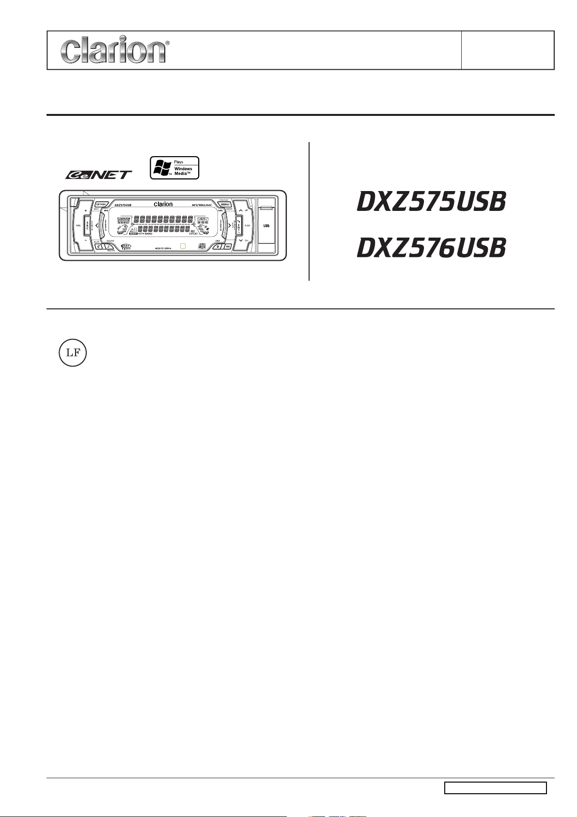
Service Manual
CD/USB/MP3/WMA/AAC Receiver
with CeNET Control
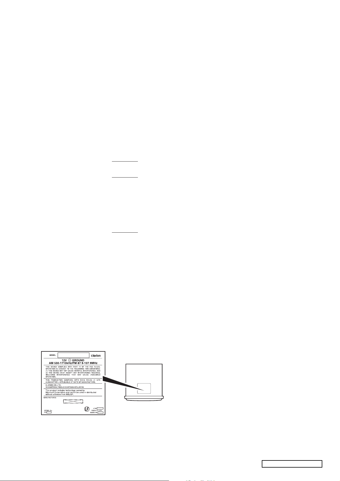
Model
Model
Published by Service Dept.
298-6407-00 MAR. 2007P
Printed in P.R.C.
(PE-2902B-A for U.S.A)
(DXZ575USB)
This product is a lead free model.
Lead free solder is used in PWB stamped LF mark.
Please keep the following conditions when you repair.
1. Use lead free solder.
* Koki's lead free solder S3X-55M 0.6mm
(CLARION Parts No.642-0231-01)
* Koki's lead free solder S3X-55M 1.0mm
(CLARION Parts No.642-0231-02)
2. Use a nitrogen solder system.
3. Do not use "General solder" and "Lead free solder"
together.
SPECIFICATIONS
FM tuner section
Frequency range: 87.9MHz to 107.9MHz
(PE-2902B-A)
87.0MHz to 108.0MHz
(PE-2902K-A/B)
Usable sensitivity: 9dBf
50dB quieting sensitivity: 15dBf
Alternate channel selectivity: 70dB
Stereo separation: 35dB(1kHz)
Frequency Response: 30Hz to 15kHz(+3/-3dB)
AM tuner section
Frequency range: 530kHz to 1710kHz
(PE-2902B-A)
531kHz to 1629kHz
(PE-2902K-A/B)
Usable sensitivity: 25uV
(PE-2902K-A/B for Other Countries)
CD player section
System: Compact disc digital audio
system
Usable discs: Compact disc
Frequency response: 5Hz to 20kHz(+1/-1dB)
Dynamic range: 95dB(1kHz)
Harmonic distortion: 0.01%
MP3/WMA/AAC mode
MP3 Sampling rate: 8kHz to 48kHz
MP3 Bit rate: 8kbps to 320kbps / VBR
WMA Bit rate: 32kbps to 192kbps
AAC Sampling rate: 8kHz to 48kHz
AAC Bit rate: 8kbps to 320kbps / VBR
Logical format: ISO9660 level1, 2
JOLIET or Romeo or APPLE ISO
file system
Audio section
Maximum power output: 53Wx4
Bass control action: +14/-14dB(80Hz)
Treble control action: +12/-12dB(10kHz)
Line output level: 5.7V(CD 1kHz)
General
Power supply voltage: 14.4V DC(10.8 to 15.6V allowable),
negative ground
Current consumption: Less than 15A
Speaker impedance: 4ohm(4ohm to 8ohm allowable)
Auto Antenna Rated Current: 500mA or less
Weight: Source unit 1.6kg
Remote control unit
40g(including battery)
Dimensions(mm): Source unit
178(W)x50(H)x158(D)
Remote control unit
44(W)x113(H)x11(D)
-1-
DXZ575USB/DXZ576USB
Page 2

NOTE
We cannot supply PWB with component parts in principle. When
*
a circuit on PWB has failure, please repair it by component parts
base. Parts which are not mentioned in service manual are not
supplied.
Specifications and design are subject to change without notice for
*
further improvement.
Use only compact discs bearing the or mark.
*
Some CDs recorded in CD-R/CD-RW mode may not be usable.
*
* Windows Media , and the Windows logo are trademarks, or re-
gistered trademarks of Microsoft Corporation in the United States
and/or other countries.
* WMA is the abbreviation of Windows Media Audio, an audio file
format developed by Microsoft Corporation.
* This product includes technology owned by Microsoft Corporation
and cannot be used or distributed without a license from MSLGP.
* As for this model, the tuner of the DSP type is used.When you
exchange it due to the tuner pack(BL1:880-2091E) trouble, it is
necessary to adjust for S-meter etc.Special JIG is necessary for
an accurate adjustment.The procedure document for the exclusive
use jig is appended to it.
* This DSP IC SAF7730HN219A(051-6706-40) of main PWB is ex-
posed die soldering pad type. The middle of this IC package is so-
ldered with the main PWB, and it cannot remove in an ordinary s-
oldering iron.Please use special removal JIG at the time of IC exc-
hange.
* This unit is compatible with USB 1.1/2.0 with maximum data tran-
sfer rates of 12 Mbps. USB memory devices that can be played by
connecting to the unit's USB connector are limited to those recog-
nized as "USB mass storage class devices"; operation is not gua-
ranteed with all USB memory devices.
* To prevent the accidental loss of data, always back up important
data on your computer.
* This unit does not support connections to a computer.In addition,
connections made through a USB hub device are also not
supported.
* Do not connect an iPod to the USB connector, since playback and
controls may not function properly.
* Insert and remove a USB memory device only when the device is
not being accessed. Connecting or disconnecting the device at the
following times may result in the loss of data:
- If the USB memory device is removed or power is disconnected
during writing to the device.
- When the device is subjected to static electricity or electric noise.
* iPod is for legal or rightholder-authorized copying only. Don't st-
eal music. iPod is a trademark of Apple Computer, Inc., registered
in the U.S. and other countries.
To engineers in charge of repair or
inspection of our products.
Before repair or inspection, make sure to follow the
instructions so that customers and Engineers in charge
of repair or inspection can avoid suffering any risk or
injury.
DXZ575USB/DXZ576USB
1. Use specified parts.
The system uses parts with special safety features against fire
and voltage. Use only parts with equivalent characteristics
when replacing them.
The use of unspecified parts shall be regarded as remodeling
for which we shall not be liable. The onus of product liability
(PL) shall not be our responsibility in cases where an accident
or failure is as a result of unspecified parts being used.
2. Place the parts and wiring back in their original positions after
replacement or re-wiring.
For proper circuit construction, use of insulation tubes, bond-
ing, gaps to PWB, etc, is involved. The wiring connection and
routing to the PWB are specially planned using clamps to keep
away from heated and high voltage parts. Ensure that they are
placed back in their original positions after repair or inspec-
tion.
If extended damage is caused due to negligence during re-
pair, the legal responsibility shall be with the repairing com-
pany.
3. Check for safety after repair.
Check that the screws, parts and wires are put back securely
in their original position after repair. Ensure for safety reasons
there is no possibility of secondary ploblems around the re-
paired spots.
If extended damage is caused due to negligence of repair, the
legal responsibility shall be with the repairing company.
4. Caution in removal and making wiring connection to the parts
for the automobile.
Disconnect the battery terminal after turning the ignition key
off. If wrong wiring connections are made with the battery connected, a short circuit and/or fire may occur. If extensive dam-
age is caused due to negligence of repair, the legal responsi-
bility shall be with the repairing company.
5. Cautions in soldering
Please do not spread liquid flux in soldering.
Please do not wash the soldering point after soldering.
6. Cautions in soldering for chip capacitors
Please solder the chip capacitors after pre-heating for replace-
ment because they are very weak to heat.
Please do not heat the chip capacitors with a soldering iron
directly.
7. Cautions in handling for chip parts.
Do not reuse removed chips even when no abnormality is ob-
served in their appearance. Always replace them with new
ones. (The chip parts include resistors, capacitors, diodes, tran-
sistors, etc).
Please make an operation test after replacement.
8. Cautions in handling flexible PWB
Before working with a soldering iron, make sure that the iron
tip temperature is around 270
iron tip repeatedly(more than three times)to the same patterns.
Also take care not to apply the tip with force.
9. Turn the unit OFF during disassembly and parts replacement.
Recheck all work before you apply power to the unit.
10. Cautions in checking that the optical pickup lights up.
The laser is focused on the disc reflection surface through the
lens of the optical pickup. When checking that the laser opti-
cal diode lights up, keep your eyes more than 30cms away
from the lens. Prolonged viewing of the laser within 30cms
may damage your eyesight.
11. Cautions in handling the optical pickup
The laser diode of the optical pickup can be damaged by elec-
trostatic charge caused by your clothes and body. Make sure
to avoid electrostatic charges on your clothes or body, or dis-
charge static electricity before handling the optical pickup.
. Take care not to apply the
-2-
Page 3
11-1. Laser diode
The laser diode terminals are shorted for transportation in order to prevent electrostatic damage. After replacement, open
the shorted circuit. When removing the pickup from the mechanism, short the terminals by soldering them to prevent this
damage.
11-2. Actuator
The actuator has a powerful magnetic circuit. If a magnetic
material is put close to it. Its characteristics will change. En-
sure that no foreign substances enter through the ventilation
slots in the cover.
11-3. Cleaning the lens
Dust on the optical lens affects performance.
To clean the lens, apply a small amount of isopropyl alcohol to
lens paper and wipe the lens gently.
COMPONENTS
PE-2902B-A/PE-2902K-A/B
1. Source unit 1
2. Remote control unit RCB-176-200 1
3. Battery(CR2025) 1
4. Mounting bracket 300-8088-00 1
5. Mounting bracket
6. DCP case 335-6035-22 1
7. Escutcheon(OUT-ES)
8. Extension lead 854-6433-50 1
9. RCA PIN CORD 855-5520-55 1
10. Parts bag
10-1. Removal key 331-2497-00 2
10-2. Screw(M1.7x6)(PE2902B-A) 716-0872-61 1
10-3. Screw(M5x8) 716-0496-51 1
10-4. Rubber part 345-3799-20 8
300-4976-00 1
370-6272-00 1
ADJUSTMENTS
ADJUSTMENT OF BUS-TUNER : 880-2091E
This adjustment sets some values of the tuner.The adjustment data is written in EEPROM(IC605).The special jig and
software are necessary for this adjustment.
* CeNET-analyzer
* Personal computer
*SG
* Adjustment-Software:Adjustment system for DSP N217
with CeNET(Ver.Y4-S024-103-20060623)
Preparation
1. Installation of software
Execute the windows installer package in the set-folde
of the writing E2P.
2. Connection
1) Connect CeNET-analyzer to the unit with the CeNETcable.
2) Connect CeNET-analyzer(MASTER/SLAVE side) to the
PC with the serial crossing cable.
3) Connect POWER-lead of CeNET-analyzer to the
POWER-lead of the unit.
4) Connect the antenna to the unit.(FM-ANT for first adjustment)
5) Turn on CeNET-analyzer,and press the RESET-button
of it.
Set up the software
1) Click [ADJ_DSP].
2) Click [open Comm PORT].(To open the COM port of
PC)
1
3) Click [Initialization of JIG].(The BUS-analyzer sounds)
4) Click [Incoming connection].(The unit is recognized to
the BUS-analyzer)
The data is displayed, and the display changes regu-
larly.
PRN data writing
1) Click [prn FILE LOAD], and select PRN-FILE.
2) Click [EEPROM WRITE], the PRN-data is write in EEPROM of the unit.
CAUTION
Use of controls, adjustments, or performance of procedures other
than those specified herein, may result in hazardous radiation ex-
posure.
The compact disc player should not be adjusted or repaired by
anyone except properly qualified service personnel.
Bottom View of DXZ575USB
Adjustments
1. FM S-meter
1) Set SG output to 65dBuV.(FM)
2) Click [Adjustment] of "FM S-Meter".(Wait until the value
stops.)
2. FM IF-Count
1) Click [Adjustment] under "FM IF-COUNT".(The FM-IFOffset data of EEPRON is effective.)
2) Click [Check], and confirm the display is within +/-500.0.
3. Set up AM IF Offset data
* Exchange the antenna for "AM-ANT-dummy"
1) Click [Adjustment] under "AM IF-COUNT".(The AM-IFOffset data of EEPRON is effective.)
2) Click [Check], and confirm the display is within +/-500.0.
4. AM S-meter
1) Set SG output to 70dBuV.(AM)
2) Click [Adjustment] of "AM S-Meter".(Wait until the value
stops.)
Finally, push the reset button of the unit.
When computer continues to freeze, click [RESET] of
"MENU", and readjust the lost adjustment point.IF not returning, press the RESET-button of CeNET-analyzer.and
restart adjustment from the first step.
-3-
DXZ575USB/DXZ576USB
Page 4
TROUBLESHOOTING
Problem
Power does not turn on.
(No sound is produced.)
Fuse is blown.
Incorrect wiring.
Cause
Measure
Replace with a fuse of the same amperage as the old fuse.
Read the attached "Installation/Wire connection Guide" once again
and wire properly.
No sound output when
operating the unit with
amplifiers or power
antenna attached.
Nothing happens when
buttons are pressed.
GeneralCD/MP3/WMA
Display is not accurate.
No sound heard. The speaker protection circuit is
No sound heard. MP3/WMA/AAC files are absent
Sound skips or is noisy.
Sound is cut or skipped.
Noise is generated or noise
is mixed with sound.
Sound is bad directly after
power is turned on.
Power antenna lead is shorted
to ground or excessive current
is required for remote-on the
amplifiers or power antenna.
The microprocessor has
malfunctioned due to noise,
etc.
DCP or main unit connectors
are dirty.
operating.
in a disc.
Files are not recognized as an
MP3/WMA/AAC file.
File system is not correct.
Compact disc is dirty.
Compact disc is heavily scratch-
ed or warped.
MP3/WMA/AAC files are not
encoded properly.
Water droplets may form on
the internal lens when the car
is parked in a humid place.
1. Turn the unit off.
2. Remove all wires attached to the power antenna lead. Check
each wire for a possible short to ground using an ohm meter.
3.Turn the unit back on.
4. Reconnect each amplifier remote wire to the power antenna lead
one by one. If the amplifiers turn off before all wires are attached,
use an external relay to provide remote-on voltage
(excessive current required).
Turn off the power, then press the
[OPEN] button and remove the DCP.
Press the reset button for about 2 seconds
with a thin rod.
Wipe the dirt off with a soft cloth moistened with cleaning alcohol.
Turn down sound volume. Function can also be restored by turning
the power off and on again.
(Speaker volume is reduced automatically when the speaker prote-
ction circuit operates).
Write MP3/WMA/AAC files onto the disc properly.
Use MP3/WMA/AAC files encoded properly.
Use ISO9660 level 1,2 or JOLIET or Romeo or APPLE ISO
file system.
Clean the compact disc with a soft cloth.
Replace with a compsct disc with no scratches.
Use MP3/WMA/AAC files encoded properly.
Let dry for about 1 hour with the power on.
Reset button
Wrong filename File system is not correct.
The USB memory device contains
no MP3/WMA/AAC files.
No sound heard
Sound is interrupted or has
USB
noise.
USB memory device is not
recognized.
Can not insert USB memory
device.
DXZ575USB/DXZ576USB
The files are not proper MP3/
WMA/ACC format.
Files are DRM copyright protected.
Connectors are loose. Disconnect the USB memory device and reconnect securely.
The MP3/WMA/AAC files are
improperly encoded.
The USB memory device is
damaged.
Connectors are loose.
The USB memory devices has
been inserted improperly.
The USB connector is broken.
Use ISO9660 level 1,2 or JOLIET or Romeo or APPLE ISO
file system.
Record MP3/WMA/AAC files properly to the USB memory device.
Use only properly encoded MP3/WMA/AAC files.
Cancel DRM protection.
Use only properly encoded MP3/WMA/AAC files.
Disconnect the USB memory device and reconnect. If the device is
still not recognized, try replacing with a different USB memory device.
Try reversing the connection direction of the USB device (usually the
brand name surface should be facing left).
Replace with a new USB memory device.
-4-
Page 5

ERROR DISPLAYS
If an error occurs, one of the following displays is displayed. Take the measures described below to eliminate the problem.
Error Display Cause Measure
CD/MP3/
WMA/AAC
CD
changer
DVD
changer
iPod
ERROR 2
ERROR 3 A CD cannot be played due to scratches, etc. Replace with a non-scratched, non-warped disc.
ERROR 6
ERROR 2 A CD inside the CD changer is not loaded. This is a failure of CD changer’s mechanism.
ERROR 3 A CD inside the CD changer cannot be played
ERROR 6 A CD inside the CD changer cannot be played
ERROR 2 A DISC inside the DVD changer cannot be played.
ERROR 3 A DISC cannot be played due to scratches, etc. Retry or replace with a non-scratched, non-warped-
ERROR 6
ERROR P Parental level error. Set the correct Parental level.
ERROR R
ERROR 1 A communication error occurs between the iPod
NO IPOD There is no iPod connected. Please connect the iPod.
A CD is caught inside the CD deck and is not ejected. This is a failure of CD deck's mechanism.
A CD is loaded upside-down inside the CD deck
and does not play.
due to scratches, etc.
because it is loaded upside-down.
A DISC inside the DVD changer cannot be
played because it is loaded upside-down.
Region code error. Eject the disc and replace correct region code disc.
and the iPod CeNET Controller.
Eject the disc then reload it properly.
Replace with a non-scratched, non-warped disc.
Eject the disc then reload it properly.
This is a failure of DVD mechanism.
disc.
Eject the disc then reload it properly.
Disconnect the iPod, then connect it again.
ERROR 1
USB
If an error display other than the ones described above appears, press the reset button.
NO FILE
DSP ERROR
Device mechanism is damaged.
USB memory device contains no audio files.
USB connector is shortcircuited or USB memory
device is overloaded.
The unit's mechanism may be damaged.
Insert USB memory device containing audio files.
Disconnect USB memory device, then hold [SRC]
button depress to turn power OFF. Then press [SRC]
button once again to turn power ON.
-5-
DXZ575USB/DXZ576USB
Page 6
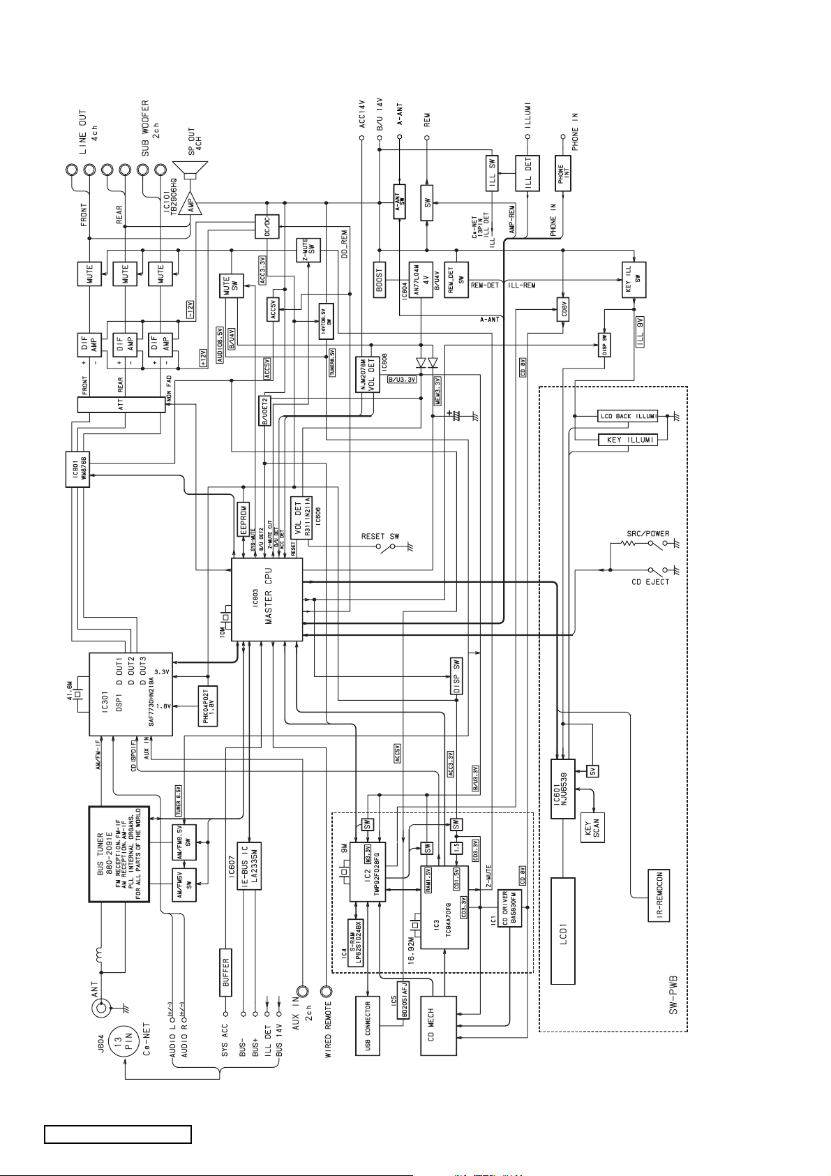
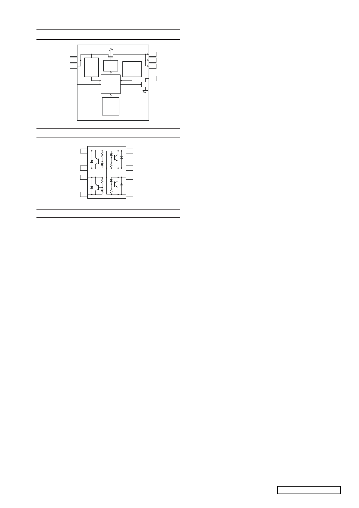
BLOCK DIAGRAM
Main section
M30873MHB-703GH
MECH PWB
USB CONTROLLER
FRONT
DXZ575USB/DXZ576USB
CD/MP3/WMA/AAC
-6-
Page 7

r
0
EXPLANATION OF IC
Main section
052-3979-01 M30873MHB-703GP Main System controller
1.Terminal Description
pin 1 : DSP SAMPLE : IN : Ground.
pin 2 : OEM-REMOCON : IN : The steering remote controller signal input.
pin 3 : IE-BUS-TX : O : IE Bus serial data output.
pin 4 : IE-BUS-RX : IN : IE Bus serial data input.
pin 5 : AUTO-ANT : O : Antenna control output.
pin 6 : BYTE(GND) : IN : Connect to VSS.
pin 7 : CNVSS : IN : Connect to VSS.
(with internal pull-down resistor)
pin 8 : XCIN : IN : The crystal resonator for sub-clock.
pin 9 : XCOUT : IN : The crystal resonator for sub-clock.
pin 10 : RESET : IN : The reset signal input.
pin 11 : X-OUT : O : The resonator for main clock.
pin 12 : GND : - : Ground.
pin 13 : X-IN : IN : The resonator for main clock.
pin 14 : VCC : - : Positive power supply.
pin 15 : VCC : IN : Positive power supply.
pin 16 : ACC-DET : IN : ACC detection signal input.
pin 17 : B/U-DET1 : IN : Backup detection signal input.
pin 18 : ILL-DET : IN : The illumination detection signal input.
pin 19 : OFFSET-DET : IN : The emergency signal input from the power IC.
pin 20 : E2P-DO : O : The serial data output to the E2PROM.
pin 21 : E2P-SCK : O : The clock pulse output to the E2PROM.
pin 22 : E2P-DI : IN : The serial data output to the E2PROM.
pin 23 : E2P-CS : O : E2PROM chip selection signal output.
pin 24 : N.C : IN : Ground.
pin 25 : RDS-CLK : IN : Ground.
pin 26 : N.C : IN : Not in use.
pin 27 : TUN-SCL : O : The clock pulse output to the BUS tunner.
pin 28 : TUN-SDA : I/O : The serial data input/output to the BUS tunner.
pin 29 : N.C : O : Not in use.
pin 30 : N.C : IN : Not in use.
pin 31 : FLASH-SCL : IN : Ground.
pin 32 : FLASH-BUSY : O : Not in use.
pin 33 : BOLERO-SDA : I/O : The serial data input/output to the BOLERO.
pin 34 : BOLERO-SCL : O : The clock pulse output when to the BOLERO.
pin 35 : Z-MUTE-CUT : O : The cut of contral signal output to the MUTE.
(CD:H:no cut; out of CD:L:cut)
pin 36 : A-MUTE(TEST) : IN : Test pin.
pin 37 : EMPH : O : Test pin.
pin 38 : BOLERO-RESET : O : The reset signal output of the BOLERO.
pin 39 : FLASH-EPM : IN : Ground.
pin 40 : N.C : IN : Not in use.
pin 41 : N.C : IN : Not in use.
pin 42 : N.C : IN : Not in use.
pin 43 : BLINKING-LED : O : BLINKING LED drive output.
pin 44 : FLASH-CE : IN : The serial data output for the flash memory.
pin 45 : P RDS TEST P1 : O : For RDS test pin
pin 46 : N.C : IN : Not in use.
pin 47 : N.C : IN : Not in use.
pin 48 : N.C : IN : Not in use.
pin 49 : N.C : IN : Not in use.
pin 50 : BOLERO-REQ : IN : The request signal input to the BOLERO.
pin 51 : AMP-MUTE : O : Muting signal output to the
Audio Power Amplifier.
pin 52 : LCD-SI/SO : I/O : The serial data input from/output to the LCD
driver
pin 53 : LCD-CE : O : Chip select signal output to the LCD driver.
pin 54 : LCD-CLK : O : The clock pulse output to the LCD driver.
pin 55 : DSP-RESET : O : Reset signal output to the DSP IC.
pin 56 : DSP-INIT : IN : The initial finished signal input from the
Radio-Audio-DSP.
pin 57 : AMP-STBY : O : ON signal output to the internal Amplifier.
pin 58 : EXT-AMP-REM : O : ON signal output to the external Amplifier.
pin 59 : NOISE-CUT : O : The cut of contral signal output to the noise.
pin 60 : VCC : - : Positive power supply.
pin 61 : N.C : IN : Not in use.
pin 62 : GND : - : Ground.
pin 63 : AM/FM-ON : O : The 8.5V power supply ON signal output.
pin 64 : AM/FM-5V-ON : O : The 5V power supply ON signal output.
pin 65 : N.C : O : Not in use.
pin 66 : N.C : O : Not in use.
pin 67 : N.C : O : Not in use.
pin 68 : N.C : O : Not in use.
-7-
pin 69 : N.C : O : Not in use.
pin 70 : N.C : IN : Not in use.
pin 71 : KEY-INT : IN : Key interrupting signal input.
pin 72 : B/U-DET2 : IN : Backup detection signal input.
pin 73 : BOLERO-ACC : O : The ACC signal of the BOLERO.
pin 74 : PHONE-IN : IN : The telephone interrupt signal input.
pin 75 : AMP-REM-DET : IN : Remote controller wire short detection.
pin 76 : N.C : O : Not in use.
pin 77 : N.C : O : Not in use.
pin 78 : N.C : IN : Not in use.
pin 79 : N.C : IN : Not in use.
pin 80 : N.C : IN : Not in use.
pin 81 : N.C : O : Not in use.
pin 82 : DISP-REM : O : The power supply control signal output for the
pin 83 : N.C : IN : Ground.
pin 84 : DD-REM : O : The control signal output for DC_DC_Converte
pin 85 : DD-F-SW : O : The frequency control signal output
pin 86 : N.C : O : Not in use.
pin 87 : N.C : O : Not in use.
pin 88 : N.C : O : Not in use.
pin 89 : KEY-A/D : IN : The input terminal of the internal ADC
pin 90 : SYS-ACC : O : ACC detection signal input.
pin 91 : SYS-MUTE : O : System muting signal output.
pin 92 : INT1 : IN : The destination setting input.
pin 93 : INT2 : IN : The destination setting input.
pin 94 : AVSS(GND) : - : Negative voltage supply for A/D converter.
pin 95 : TEST : O : Test pin.
pin 96 : VREF : IN : Reference vlotage input for A/D converter .
pin 97 : AVDD : - : Positive voltage supply for A/D converter.
pin 98 : DSP-SCL : O : I2BUS serial clock output
pin 99 : DSP-SDA : I/O : I2BUS serial data input/output
pin10
: N.C : IN : Not in use.
051-9126-30 LP62S1024BX-70LLIF 128 x 8 b it SRAM
Terminal Description
pin 1: A 11 : IN : Address signal input.
pin 2: A 9 : IN : Address signal input.
pin 3: A 8 : IN : Address signal input.
pin 4: A 13 : IN : Address signal input.
pin 5: WE_ : IN : Write enable signal input.
pin 6: CE 2 : IN : The chip enable signal input.
pin 7: A 15 : IN : Address signal input.
pin 8: VCC : - : Positive voltage supply.
pin 9 : NU : - : Not in use.
pin 10: A 1 6 : IN : Address signal input.
pin 11: A 1 4 : IN : Address signal input.
pin 12: A 1 2 : IN : Address signal input.
pin 13: A 7 : IN : Address signal input.
pin 14: A 6 : IN : Address signal input.
pin 15: A 5 : IN : Address signal input.
pin 16: A 4 : IN : Address signal input.
pin 17: A 3 : IN : Address signal input.
pin 18: A 2 : IN : Address signal input.
pin 19: A 1 : IN : Address signal input.
pin 20: A 0 : IN : Address signal input.
pin 21 : D 0 :I/O: Data input/output.
pin 22 : D 1 :I/O: Data input/output.
pin 23 : D 2 :I/O: Data input/output.
pin 24: GND : - : Ground.
pin 25 : D 3 :I/O: Data input/output.
pin 26 : D 4 :I/O: Data input/output.
pin 27 : D 5 :I/O: Data input/output.
pin 28 : D 6 :I/O: Data input/output.
pin 29 : D 7 :I/O: Data input/output.
pin 30: CE 1_ : IN : The chip enable signal input.
pin 31: A 1 0 : IN : Address signal input.
pin 32: OE_ : IN : Output enable signal input.
Truth Table
WE_ CE1_ CE2 OE_
(pin 5) (pin 30) (pin 6) (pin 32) I/O Operation
x H x x High Z
x x L x High Z
HLHH HighZ
H L H L data out
L L H x data in
displayer.
for DC_DC_Converter.
for key judgment.
for the Radio-Audio-DSP.
for the Radio-Audio-DSP.
DXZ575USB/DXZ576USB
Page 8

051-6706-40 SAF7730HN219A Main system controller
:-:
:
:IN:
:
:
:
:IN:
:
:IN:
:
:IN:
:
:-:
:
:-:
:
:-:
:
:-:
:
:IN:
:
:
:IN:
:
:IN:
:
:IN:
:
:
:IN:
:
:IN:
:
:-:
:
:-:
:
:-:
:
:-:
:
:O:
:
:IN:
:
:-:
:A0:-:
:
:IN:
:
:
:
:-:
:
:O:
:
:IN:
:
:-:
:
:IN:
:
:
:IN:
:
:
:O:
:
:O:
:
:-:
:
:-:
:
:-:
:
:O:
:
:O:
:
:
:
:-:
:
:
:
:-:
:
:-:
:
:IN:
:
:IN:
:
:IN:
:
:-:
:
:-:
:
:
:
:O:
:
:
:
:O:
:
:-:
:
:-:
:
:IN:
:
:IN:
:
:IN:
:
:IN:
:
:IN:
:
:IN:
:
:-:
:
:-:
:
:-:
:
:-:
:
:IN:
:
:IN:
:
:IN:
:
:IN:
:
:O:
:
:O:
:
:O:
:
:O:
:
:
:
:
:
:
:
:
:
:-:
:
:-:
:
:
:
:
:
:
:
:
:
:-:
:
:IN:
:
:
:
:
:
:
:
:
pin100
:
pin101
:
pin102
:
:
pin103
:
:
pin104
:
:-:
pin105
:
:-:
pin106
:
pin107
:
pin108
:
:O:
pin109
:
:O:
pin110
:
:O:
pin111
:
:O:
pin112
:
pin113
:
pin114
:
pin115
:
:O:
pin116
:
:O:
pin117
:
:O:
pin118
:
pin119
:
pin120
:
pin121
:
:-:
pin122
:
:-:
pin123
:
:
pin124
:
:
pin125
:
:-:
pin126
:
:-:
pin127
:
:O:
pin129
:
:-:
pin130
:
:-:
pin131
:
:IN:
pin132
:
:O:
pin133
:
:-:
pin134
:
:O:
pin135
:
:O:
pin136
:
:IN:
pin137
:
:IN:
pin138
:
:-:
pin139
:
:-:
pin140
:
:-:
pin141
:
:-:
pin142
:
:-:
pin143
:
:IN:
pin144
:
:IN:
1.Terminal Description
pin 1:VDDA_1V8
AUX_R
pin 2
AUX_R_GND:IN:Right common mode reference auxiliary input.
pin 3
AUX_L_GND:IN:Left common mode reference auxiliary input.
pin 4
AUX_L
pin 5
pin 6
TAPE_R
TAPE_L
pin 7
VADCP
pin 8
VDD_ADC
pin 9
VADCN
pin 10
VREFAD
pin 11
CD_R
pin 12
CD_R_GND:IN:Right common mode reference CD input.
pin 13
CD_L_GND
pin 14
pin 15
CD_L
PHONE_IN
pin 16
PHONE_GND:IN:Common reference audio phone input.
pin 17
NAV
pin 18
NAV_GND
pin 19
VDDD1
pin 20
VSSS1
pin 21
TRSTN
pin 22
pin 23
TCK
N.C
pin 24
TDI
pin 25
TMS
pin 26
pin 27
pin 28
SCL
SDA
pin 29
GAPREG
pin 30
CONREG
pin 31
FEBREG
pin 32
VDD_REG
pin 33
SPDIF_IN1
pin 34
pin 35
VSS_SPDIF:IN:Ground supply for spdif input.
SPDIF_IN2
pin 36
VDD_SPDIF:IN:3.3V supply for spdif input.
pin 37
DAC_RR
pin 38
DAC_RL
pin 39
pin 40
VDACP
VDACN
pin 41
VDD_DAC
pin 42
DAC_FR
pin 43
DAC_FL
pin 44
DAC_SUBW:O:Audio output for subwoofer.
pin 45
DAC_CENTER:O:Audio output for center speaker.
pin 46
VDDQ1
pin 47
pin 48
FS_SYS
RESETN
pin 49
TEST1
pin 50
BCK_IN1
pin 51
WS_IN1
pin 52
SD_IN1
pin 53
pin 54
VDDD2
VSSS2
pin 55
N.C
pin 56
N.C
pin 57
N.C
pin 58
N.C
pin 59
N.C
pin 60
VSSS5
pin 61
pin 62
BCK_IN2
WS_IN2
pin 63
SD_IN2
pin 64
BCK_IN3
pin 65
WS_IN3
pin 66
SD_IN3
pin 67
VSSQ1
pin 68
VDDQ2
pin 69
pin 70
ADSP_IOF5
ADSP_IOF6
pin 71
BCK_IN4
pin 72
1.8V supply for IFADC and Audio ADCs.
Right channel of auxiliary input.
Left channel of auxiliary input.
Right channel of tape input.
Left channel of tape input.
Positive reference voltage for Audio ADCs.
3.3V supply for audio ADCs.
Ground reference for audio ADCs.
Common mode reference voltage ADCs.
Right channel of CD input.
Left common mode reference CD input.
Right channel of CD input.
Audio phone input.
Audio navigation input.
Common reference audio navigation input.
1.8V positive supply.
Ground supply.
Test reset, active low.
Test clock.
Not in use.
Test control data input.
Test mode select.
Slave sub-address I2C selection.
Serial clock input I2C bus.
I/O:Serial data input / output I2C bus.
Decoupling for regultator bandgap voltage.
Control output for external PMOS transistor.
Feedback input monitoring the 1.8V.
3.3V supply for regulator.
Spdif input1.
Spdif input2.
Audio output for Rear-right speaker.
Audio output for Rear_left speaker.
Positive reference voltage for audio DACs.
Ground reference voltage for audio DACs.
3.3V supply for audio DACs.
Audio output for Front-right speaker.
Audio output for Front-left speaker.
Positive supply (peripheral cells only).
I/O:FS system clock in/output.
General reset of chip (active low).
Test pin1 reserved for digital testing.
IIS source 1 Bit Clock input.
IIS source 1 Word Select input.
IIS source 1 Data input.
1.8V positive supply.
Ground supply.
I/O:Not in use.
Not in use.
I/O:Not in use.
Not in use.
1.8V positive supply (for memories only).
Ground supply (for memories).
IIS source 2 Bit Clock input.
IIS source 2 Word Select input.
IIS source 2 Data input.
IIS source 3 Bit Clock input.
IIS source 3 Word Select input.
IIS source 3 Data input.
Ground supply (peripheral cells only).
Positive supply (peripheral cells only).
Audio DSP general purpose I/O flag 5.
Audio/SRC DSP general purpose I/O flag 6.
IIS source 4 Bit Clock input.
pin 72
BCK_IN4
WS_IN4
pin 73
SD_IN4
pin 74
pin 75
SD_HOST_OUT1
pin 76
SD_HOST_OUT2
pin 77
SD_HOST_OUT3
pin 78
N.C
WS_HOST
pin 79
BCK_HOST:I/O:Host IIS Bit Clock output/input.
pin 80
SD_HOST_IN1:IN:Host IIS 1 Data input.
pin 81
SD_HOST_IN2:IN:Host IIS 2 Data input.
pin 82
SD_HOST_IN3:IN:Host IIS 3 Data input.
pin 83
SD_HOST_IN4:IN:Host IIS 4 Data input.
pin 84
SD_HOST_IN5:IN:Host IIS 5 Data input.
pin 85
VSSQ2
pin 86
pin 87
VDDQ3
ADSP_IOF7:I/O:Audio/SRC DSP general purpose I/O flag 7.
pin 88
ADSP_IOF8:I/O:Audio/SRC DSP general purpose I/O flag 8.
pin 89
ADSP_IOF9:I/O:Audio/SRC DSP general purpose I/O flag 9.
pin 90
N.C
pin 91
pin 92
ADSP_IOF11:I/O:Audio/SRC DSP general purpose I/O flag 11.
N.C
pin 93
pin 94
VDDD3
VSSS3
pin 95
N.C
pin 96
N.C
pin 97
N.C
pin 98
N.C
pin 99
IIS source 4 Bit Clock input.
IIS source 4 Word Select input.
IIS source 4 Data input.
Host IIS 1 Data output.
Host IIS 2 Data output.
Host IIS 3 Data output.
Not in use.
I/O:Host IIS Word Select output/input.
Ground supply (peripheral cells only).
Positive supply (peripheral cells only).
I/O:Not in use.
I/O:Not in use.
1.8V positive supply.
Ground supply.
I/O:Not in use.
I/O:Not in use.
I/O:Not in use.
I/O:Not in use.
TDSP_IOF5:I/O:Tuner DSP general purpose I/O flag 5.
TDSP_IOF6:I/O:Tuner DSP general purpose I/O flag 6.
N.C
N.C
VSSQ3
VDDQ4
I/O:Not in use.
I/O:Not in use.
Ground supply (peripheral cells only).
Positive supply (peripheral cells only).
TDSP_IOF9:I/O:Tuner DSP general purpose I/O flag 9.
TDSP_IOF10:I/O:Tuner DSP general purpose I/O flag 10.
N.C
N.C
AGC2_1
AGC2_2
Not in use,
Not in use.
LSB Gain control output 1 to DICE2.
MSB Gain control output 2 to DICE2.
TDSP_IOF11:I/O:Tuner DSP general purpose I/O flag 11.
TDSP_IOF12:I/O:Tuner DSP general purpose I/O flag 12.
ADSP_IOF4:I/O:Audio DSP general purpose I/O flag 4
(e.g. IBOC_BLEND).
SD_IBOC_OUT_I
SD_IBOC_OUT_Q
WS_IBOC_OUT
Serial data output IBOC I-signal.
Serial data output IBOC Q-signal.
IBOC Word Select output.
BCK_IBOC_:O:IBOC Bit Clock output.
RESERVED_:-:Reserved.
RESERVED_:-:Reserved.
VSSS6
VDD_MEM2
N.C
N.C
VDDD4
VSSS4
N.C
Ground supply (for memories).
1.8V positive supply (for memories only).
I/O:Not in use.
I/O:Not in use.
1.8V positive supply.
Ground supply.
Not in use.
pin128 : N.C : O : Not in use.
VSSQ4
VSS_OSC
OSC_IN
OSC_OUT
VDD_OSC
N.C
KAGC2
IFAD_N1
IFAD_P1
VSS_IFAD
VDD_IFAD
VIFADP
VIFADN
VIFADBG
IFAD_P2
IFAD_N2
Ground supply (peripheral cells only).
Ground supply for oscillator and PLLs.
Crystal oscillator input.
Crystal oscillator output.
1.8V supply for oscillator and PLLs.
Not in use.
Keyed AGC DAC output 2.
Negative phase of the first differential IF input.
Positive phase of the first differential IF input.
Ground supply for IF ADCs.
3.3V supply for IF ADCs.
Decoupling for IF ADCs positive reference voltage.
Ground reference voltage for IF ADCs.
Decoupling for IF ADCs bandgap voltage.
Positive phase of the second differential IF input.
Negative phase of the second differential IF input.
DXZ575USB/DXZ576USB
-8-
Page 9
051-6926-90 BD2051AFJ-TR MECH System controller
1Ground 8 Output
(Positive
Logic)
2Input
Under
Voltage
3Input
Down
4Enable Input
Shut
Charge
Pump
Logic
Thermal
Shut
Down
Over
Current
Detection
7 Output
6 Output
Over
Current
5
Detection
Output
(Negative
Logic)
051-6927-90 SN65240PWR Main System controller
1GND 8A
2C
3GND
4D
7 GND
6B
5 GND
052-3981-90 TMP92FD28FG Main System Controller
Terminal Description
pin 1: RESET : IN : Reset signal input.
pin 2: BU DET :IN : Backup detection signal input.
pin 3: ACC DET : IN : ACC detection signal input.
pin 4: SBSY : IN : Sub code block synchronous signal detec-
pin 5: LIMIT : IN : Inside limit switch signal input for the pick-
tion input.
up.
pin 6: D VCC : - : Positive voltage supply.
pin 7: X T 1 : IN : Crystal connection.
pin 8: X T 2 : O : Crystal connection.
pin 9: PW E : O : External power supply control output.
pin 10 : D V S S : - : Digital ground.
pin 11 : D V CC : - : Positive voltage supply.
pin 12 : Vref : O : Reference voltage output.
pin 13 : VREFI : IN : Reference voltage input.
pin 14 : VREFI : IN : Reference voltage input.
pin 15 : Vref : O : Reference voltage output.
pin 16 : D V CC : - : Positive voltage supply.
pin 17 : D V S S : - : Digital ground.
pin 18 : D 0 :I/O: Data input/output.
pin 19 : D 1 :I/O: Data input/output.
pin 20 : D 2 :I/O: Data input/output.
pin 21 : D 3 :I/O: Data input/output.
pin 22 : D 4 :I/O: Data input/output.
pin 23 : D 5 :I/O: Data input/output.
pin 24 : D 6 :I/O: Data input/output.
pin 25 : D 7 :I/O: Data input/output.
pin 26 : D V S S : - : Digital ground.
pin 27 : D V CC : - : Positive voltage supply.
pin 28: R E Q O : O : Request signal output.
pin 29: LD CONT : O : Loading signal output.
pin 30: LD MUTE : O : Muting signal output to the CD mecha-
nism.
pin 31: DR MUTE : O : Drive mute signal output to the CD IC.
pin 32: P O N 1 : O : Power ON signal output.
pin 33: PO N 2 : O : Power ON signal output.
pin 34: TR A : IN : Photo sensor signal input from the CD
pin 35: TR B : IN : Photo sensor signal input from the CD
mechanism.
mechanism.
pin 36: A 0 : O : Address signal output.
pin 37: A 1 : O : Address signal output.
pin 38: A 2 : O : Address signal output.
pin 39: A 3 : O : Address signal output.
pin 40: A 4 : O : Address signal output.
pin 41: A 5 : O : Address signal output.
pin 42: A 6 : O : Address signal output.
pin 43: A 7 : O : Address signal output.
pin 44 : D V S S : - : Digital ground.
pin 45 : D V CC : - : Positive voltage supply.
pin 46: A 8 : O : Address signal output.
pin 47: A 9 : O : Address signal output.
pin 48: A 1 0 : O : Address signal output.
pin 49: A 1 1 : O : Address signal output.
pin 50: A 1 2 : O : Address signal output.
pin 51: A 1 3 : O : Address signal output.
pin 52: A 1 4 : O : Address signal output.
pin 53: A 1 5 : O : Address signal output.
pin 54: A 1 6 : O : Address signal output.
pin 55: BUS 0 :I/O: Data input / output.
pin 56: BUS 1 :I/O: Data input / output.
pin 57: BUS 2 :I/O: Data input / output.
pin 58: BUS 3 :I/O: Data input / output.
pin 59: BU CLOCK : O : Clock pulse output.
pin 60: CCE : O : Chip enable signal output.
pin 61: CD RESET : O : Reset pulse output.
pin 62 : D V S S : - : Digital ground.
pin 63 : D V CC : - : Positive voltage supply.
pin 64: RD : O : Read enable flag output.
pin 65: S-RAM WR : O : Write command output to the S-RAM.
pin 66: HSSW : IN : Through mode setting.
pin 67: HSSW 2 : IN : Through mode setting.
pin 68: SRAM STND : O : SRAM standby output.
pin 69 : BOOT :IN : Flash Memory Write mode selection.
pin 70: CHIP SEL : O : Chip select signal output.
pin 71: LR CK : O : LR clock output.
pin 72 : AM 1 : IN : Function Mode.
pin 73 : X 2 : - : Crystal connection.
pin 74 : D V S S : - : Digital ground.
pin 75 : X 1 : - : Crystal connection.
pin 76 : D V CC : - : Positive voltage supply.
pin 77: USB OC :IN : USB over current.
pin 78: USB P ON : O : USB opwer on.
pin 79: USB D+IO :I/O: USB D+.
pin 80: USB D-IO :I/O: USB D-.
pin 81 : AM 0 : IN : Function Mode.
pin 82: DSP REQ : IN : DSP request input.
pin 83 : D V S S : - : Digital ground.
pin 84 : TEST : O : F o r t h e t est.
pin 85: P O N 3 : O : Power ON signal output.
pin 86: SD CS : O : SD chip select output.
pin 87: SD Data O : O : SD data output.
pin 88: SD Data I : IN : SD data input.
pin 89: SD CK : IN : SD clock input.
pin 90: S D A :I/O: Serial data input/output.
pin 91: S C K : IN : Serial clock pulse input.
pin 92: B C K : O : Bit clock output.
pin 93 : DATA : O : DATA output.
pin 94: GATE : O : Gate signal input.
pin 95 : D VC C : - : Positive voltage supply.
pin 96: CHUCK : IN : CD MECHA CHUCK
pin 97: S D W P : IN : SD write protection.
pin 98: SD Detect : IN : SD Card detection.
pin 99: ST RE Q : IN : Request signal input.
pin100: D VSS : - : Digital ground.
-9-
DXZ575USB/DXZ576USB
Page 10

EXPLODED VIEW / PARTS LIST
DCP section
1-4
1-7
1-1
1-12
1-8
1-11
1-9
1-2
1-19
1-13
1-5
1-8
1-20
1-6
1-28
1-24
1-11
1-16
1-10
1-11
1-10
1-23
1-9
1-21
1-17
1-7
1-30
1-10
1-18
1-10
1-22
1-32
1-3
1-25
1-23
1-14
1-26
1-49
1-15
1-34
1-10
1-27
1-33
1-10
1-29
1-33
1-31
1-35
1-43
1-47
1-43
1-42
1-36
1-36
1-48
1-44
1-37
1-38
1-45
1-46
1-39
1-47
1-40
1-43
1-43
1-43
1-34
1
Note) Some parts depend on
each model. The model name
is specified in the description.
1-41
: SANKOL application
Note) SANKOL uses G-311S
NO PART NO DESCRIPTION Q'TY NO PART NO DESCRIPTION Q'TY
1 DCP-587-600 DCP ASSY(PE-2902B-A) 1 1-23 335-7985-01 INDICATOR-A 2
DCP-587-800 DCP ASSY(PE-2902K-A/B) 1 1-24 382-8175-00 BUTTON 1
1-1 335-7724-00 BRAND 1 1-25 382-8176-00 BUTTON 1
1-2 373-1125-05
373-1125-09
SEEK PANEL(PE-2902B-A)
SEEK PANEL(PE-2902K-A/B)
1 1-26 382-8179-00 BUTTON 1
1 1-27 382-8177-00 BUTTON 1
1-3 382-8178-00 BUTTON 1 1-28 335-7997-00 ILLUMI PLATE 1
1-4 382-8171-00 BUTTON 1 1-29 335-7996-00 ILLUMI PLATE 1
1-5 347-8246-00 LEATHER SHEET 1 1-30 345-5979-00 RUBBER KEY 1
1-6 347-8245-00 LEATHER SHEET 1 1-31 345-5980-00 RUBBER KEY 1
1-7 347-8208-00 LEATHER SHEET 4 1-32 335-7998-00 REAR CVR 1
1-8 347-8210-00 TRIM CVR 2 1-33 716-0872-62 SCREW(M1.7x8) 4
1-9 335-8004-00 ROLLER 2 1-34 345-5983-00 RUBBER SPACER 4
1-10 716-0872-51 SCREW(M1.7x6) 6 1-35 379-1382-51 INDICATOR(LCD) 1
1-11 347-8251-00 FILM 6 1-36 345-5981-00 RUBBER CONNECTOR 2
1-12 382-8170-00 REL BUTTON 1 1-37 347-8152-00 BLACK FILM 1
1-13 750-6720-00 SPRING 1 1-38 347-8153-00 FILM 1
1-14 370-6262-01
370-6262-00
ESCUTCHEON(PE-2902B-A)
ESCUTCHEON(PE-2902K-A/B)
1 1-39 335-7999-00 ILLUMI PLATE 1
1 1-40 335-8000-00 LCD HOLDER 1
1-15 335-7984-00 IR FILTER 1 1-41 331-4378-00 LCD CVR 1
1-16 335-7989-00 SPRING CAP 2 1-42
---------------
SWITCH PWB 1
1-17 750-6856-00 SPRING 1 1-43 013-6524-50 SWITCH 5
1-18 335-7992-00 SPRING CVR 1 1-44 013-7419-00 SWITCH 1
1-19 382-8172-00 BUTTON 1 1-45 060-4017-90 IR RECEIVER 1
1-20 382-8173-00 BUTTON 1 1-46 001-7046-01 DIODE 1
1-21 382-8180-00 BUTTON 1 1-47 001-7040-91 LED 2
1-22 382-8174-01 BUTTON 1 1-48 076-0647-00 PLUG 1
1-49 382-8343-00 BUTTON 1
DXZ575USB/DXZ576USB
-10-
Page 11

Inner Escutcheon section
13
12
10
3
14
8
7
6
5
4
2
SANKOL
application
11
20
21
Grease application
1
(spring immerge
into grease)
22
24
23
19
14
18
15
18
32
SANKOL
application
25
16
Grease
application
23
33
26
9
17
Finished figure
34
27
29
31
23
30
28
Note) SANKOL uses CFD-409Z, Grease uses G-311S.
NO.
PART NO. DESCRIPTION
1
345-6048-00 CUSHION
2
345-5982-00 USB-CAP
3
347-8232-00 SHADE
4
335-6499-00 CN-CVR
5
335-6501-01 HOOK DCP
6
750-3454-00 SPRING
7
341-1764-00 SHAFT
8
346-0097-00 LEATHER SHEET
9
780-2004-51 SCREW(M2 x 4) 1
10
370-6263-00 INNER-ES
11
335-6886-00 ILLUMI PLATE
12
331-4380-00 FRONT PLATE
13
335-7369-01 HOOK
14
716-3546-51 SCREW(M2x0.4)
15
750-3341-00 SPRING
16
716-0872-51 SCREW(M1.7x6)
17
613-0730-00 GEAR DAMPER
Q'TY NO.
118
119
120
121
122
1
123
124
25
126
127
128
129
230
131
432
133
34
Grease
application
PART NO. DESCRIPTION
716-0778-52 SCREW(M2x8)
855-0612-50 USB CABLE
347-7008-00 FPC SUPPORT
074-1278-01 OUTLET SOCKET(16P)
039-1862-01 INNER ES FPC
(WITHOUT COMPONENT)
738-1722-1H PRECISION
716-3444-50 SCREW(M1.7
SCREW(M1.7x2.2)
)
347-6356-00 DOUBLE FACE
335-6502-00 SLIDER
291-0092-00 STICKER
743-1500-10 E-RING
613-0684-00 FAN GEAR
335-8001-00 HOOK
290-0168-00 LABEL
750-3342-21 SPRING
331-4379-00 DCP HOLDER
341-1830-00 SHAFT
Q'TY
2
1
1
1
1
5
2
1
1
1
1
1
1
1
1
1
1
- 11-
DXZ575USB/DXZ576USB
Page 12

Main section
33
32
31
29
29
29
31
29
43
42
30
17
44
41
29
27
40
22
25
39
19
17
17
19
26
19
17
18
17
21
20
9
35
23
Inner escutcheon
37
36
NO.
PART NO. DESCRIPTION
1
074-2244-68 OUTLET SOCKET
2
305-0336-01 SIDE-CVR(L)
3
880-2091E TUNER
4
074-1214-50 OUTLET SOCKET(16P)
5
331-3954-00 IC-HOLDER
6
076-0368-16 PLUG(16P)
7
076-6003-18 PLUG(18P)
8
074-1194-00 OUTLET SOCKET(Ce-NET)
9
307-0723-01 REAR-CVR 1
10
313-1924-00 HEAT SINK
11
714-3005-8B MACHINE SCREW(M3 x 5)
12
305-0337-00 SIDE-CVR(R)
13
074-1138-79 OUTLET SOCKET(20P)
14
013-6103-00 TACT SWITCH
15
001-7062-90 DIODE
16
17
18
19
20
21
22
23
------------ MAIN PWB
731-3006-8B TAPTIGHT(M3 x 6)
092-2215-50 ANT-RECEPT
714-3006-8B MACHINE SCREW(M3 x 6)
074-0898-16 OUTLET SOCKET(16P)
------------ D/D PWB
313-1923-00 HEAT SINK
780-2607-52 SCREW(M2.6 x 7)
34
28
17
29
Q'TY NO.
124
125
126
127
128
129
130
131
133
434
135
136
137
138
1
8
139
740
141
142
143
244
28
5
4
6
3
2
1
16
15
14
38
13
12
7
11
PART NO. DESCRIPTION
347-7580-10 SHADE
331-4073-00 STOPPER
347-7581-10 CUSHION
303-0472-07 UPPER CASE
716-1670-01 SCREW(M2x4)
714-2603-8B MACHINE SCREW(M2.6 x 3)
331-4376-00 MECH-BRKT(R)
347-6821-00 SPCER FILM
32
929-5016-80 CD-MECH MODULE
816-4026-50 FLAT WIRE
331-4367-01 MECH BRKT(F)
347-8250-00 DOUBLE FACE
347-7578-10 INSULATOR
304-0483-00 LOWER-CVR
276-0173-00 SETPLATE(PE-2902B-A)
276-0245-00 SETPLATE(PE-2902K-A) 1
276-0246-00 SETPLATE(PE-2902K-B) 1
331-4312-01 EARTH PLATE
074-1228-79 OUTLET SOCKET(29P)
074-1138-60 OUTLET SOCKET(10P)
074-1138-65 OUTLET SOCKET(15P)
076-0478-55 OUTLET SOCKET(5P)
------------ MECH PWB
8
17
24
10
19
11
17
Q'TY
1
1
2
1
2
7
1
2
1
1
1
1
1
1
1
1
1
1
1
1
1
DXZ575USB/DXZ576USB
-12-
Page 13

CD mechanism section: 929-5016-80
B1
71
H1
46
H2
22
B2
29
H3
23
73
A1
34
63
1
72
48
H4
H5
G6
44
68
A4
65
75
D1
G13
H6
A4
H7
52
H3
H1
H2
70
to MAIN
31
B1
22
G2
26
H6
G13
29
60
G12
A1
3
H5
H4
A3
D2
21
62
A8
64
B2
1
65
47
67
2
35
G6
66
61
9
A5
25
G3
K1
C3
K2
7
E2
G12
M1
A2
50
43
18
11
G14
G14
K3
K4
17
G2
41
6
C2
G5
C1
24
37
G4
G5
A3
57
E2
66
G1
G9
C5
G8
20
G11
38
42
39
8
E1
G3
M1
32
40
G4
K3
K4
56
54
27
58
10
E1
G11
G8
G9
C5
33
55
53
51
30
74
G1
59
D1
12
A8
59
D2
A2
46
5
A5
13
69
45
36
H6
49
C1
14
H6
H7
-13-
4
49
K1
C3
K2
16
28
DXZ575USB/DXZ576USB
15
19
C2
Page 14

NO.
PART NO. DESCRIPTION
1 ----------- SENSOR PWB 1 38 621-1749-20 POWER GEAR B 1
2 966-1743-21 DRIVE-PLT-ASSY 1 39 621-1750-20 POWER GEAR C 1
3 SMA-182-100 SPINDLE MOTOR-ASSY 1 40 621-1751-20 POWER GEAR D 1
4 SMA-197-100 SLED MOTOR-ASSY 1 41 621-1752-20 DISC STOPPER 1
5 345-5476-20 CUSHION RUBBER 1 42 621-1753-20 CLAMPER RING 1
6 620-1023-23 CLAMPER PLATE 1 43 621-1754-20 GEAR BASE 1
7 620-1026-21 SPRING PLATE 1 44 622-1571-21 ROLLER SHAFT 1
8 620-1596-23 CLAMPER LINK 1 45 624-0020-00 LEAD SCREW 1
9 620-1598-22 UPPER CHASSIS 1 46 629-0086-20 DAMPER F 2
10 620-1752-20 SENSOR ARM 1 47 629-0087-20 DAMPER R 1
11 620-1753-20 ID-LOCK PLATE 1 48 716-1507-01 SCREW(M2x3) 1
12 620-1766-20 LOWER CHASSIS 1 49 716-1670-01 SCREW(M2x4) 4
13 621-0608-21 SECOND GEAR 1 50 716-1733-01 SCREW(M1.7x2.3) 2
14 621-0609-20 BASE GEAR 1 51 716-3469-01 SCREW(1.7x4) 2
15 621-0610-20 IDLE GEAR A 1 52 716-3473-01 SCREW(M2x3) 1
16 621-0611-20 IDLE GEAR B 1 53 716-3551-00 SCREW(M1.4x2.5) 2
17 621-0612-21 ROLLER GEAR A 1 54 750-3467-21 SHIFT SPRING 1
18 621-0620-20 THREAD GEAR A 1 55 750-3468-20 RACK SPRING 1
19 621-0621-20 THREAD GEAR B 1 56 750-3469-20 CLAMPER SPRING 1
20 621-0623-23 LS-HOLDER 1 57 750-3470-20 ID-LOCK SPRING 1
21 621-0624-22 GUIDE RAIL 1 58 750-3471-20 SENSOR SPRING 1
22 621-0711-20 LOADING ROLLER 2 59 750-3472-21 DR-SPRING F 2
23 621-0718-21 ROLLER GUIDE 1 60 750-3473-20 DR-SPRING RA 1
24 621-0719-20 ROLLER GEAR 1 61 750-3474-20 DR-SPRING RB 1
25 621-0720-20 ROLLER GEAR C 1 62 750-3475-21 DR-SPRING C 1
26 621-0721-20 ROLLER GEAR D 1 63 750-6797-20 ROLLER SPRING L 1
27 621-0728-20 STOPPER LINK 1 64 750-6798-20 ROLLER SPRING R 1
28 621-1719-20 IDLE CASE 1 65 714-2003-8B SCREW(M2x3) 2
29 621-1726-20 ROLLER SLEEVE 2 66 780-2025-00 SCREW(M2x2.5) 3
30 621-1729-20 SH-BASE 1 67 781-1730-00 SCREW(M1.7x3) 1
31 621-1742-20 UPPER GUIDE 1 68 803-4906-60 VINYL-COAT-WIRE(ORG) 1
32 621-1743-20 SHIFT LEVER 1 69 969-0071-30 PICKUP-ASSY 1
33 621-1744-20 RACK 1 70 816-2590-00 SPECIAL LEAD(GRN) 1
34 621-1745-20 LOCK ARM L 1 71 816-2591-00 SPECIAL LEAD(YEL) 1
35 621-1746-20 LOCK ARM R 1 72 816-2592-00 SPECIAL LEAD(BLUE) 1
36 621-1747-20 GEAR COVER 1 73 816-2593-00 SPECIAL LEAD(PUR) 1
37 621-1748-20 POWER GEAR A 1 74 966-1722-20 SH-RACK-ASSY 1
Q'TY NO.
PART NO. DESCRIPTION
75 816-2624-50 FLAT WIRE 1
Q'TY
ELECTRICAL PARTS LIST
Main PWB(B1) section
REF No. PART No. DESCRIPTION REF No. PART No. DESCRIPTION REF No. PART No. DESCRIPTION
ANT1
BL1 880-2091E
C2 043-1719-90 22pF C104 042-0654-52 6.3V 10uF C123 043-1751-90 4700pF
C3 042-1631-50 10VL 100uF C105 042-0654-52 6.3V 10uF C124 043-1804-90 0.1uF
C4 043-1802-90 0.01uF C106 042-0654-52 6.3V 10uF C125 043-1751-90 470pF
C5 043-1821-90 0.022pF C107 042-0654-52 6.3V 10uF C126 043-1751-90 470pF
C7 043-1800-90 1000pF C108 042-0654-52 6.3V 10uF C127 043-1751-90 470pF
C8 187-4763-15 6.3V 47uF C109 042-0654-52 6.3V 10uF C128 043-1751-90 470pF
C9 043-1608-90 0.1uF C110 163-2253-65 50V 2.2uF C129 043-1751-90 470pF
C9 046-1042-78 0.1uF C114 178-4742-78 25V 0.47uF C130 043-1751-90 470pF
C10 043-1804-90 0.1uF C115 178-4742-78 25V 0.47uF C131 043-1751-90 470pF
C11 043-1739-90 150pF C116 178-4742-78 25V 0.47uF C132 043-1751-90 470pF
C12 043-1735-90 100pF C117 178-4742-78 25V 0.47uF C133 043-1800-90 1000pF
C13 043-1735-90 100pF C118 043-1751-90 470pF C138 043-1800-90 1000pF
C14 043-1800-90 1000pF C119 163-1053-65 50V 1uF C139 043-1800-90 1000pF
C15 043-0552-90 6.3V 47uF C120 163-1063-35 16V 10uF C301 178-4742-78 25V 0.47uF
DXZ575USB/DXZ576USB
092-2215-50
ANT-RECEPT
TUNER
Note)Several different parts of the same reference number are alternative parts.
One of those parts is used in the set.
Some parts depend on each model. The model name is specified in the description.
C101 042-1715-00 16V 3300pF C121 043-1751-90 470pF
C102 172-1041-15 50V 0.1uF C122 043-1751-90 470pF
-14-
Page 15

REF No. PART No. DESCRIPTION REF No. PART No. DESCRIPTION REF No. PART No. DESCRIPTION
C302 043-0540-00 6.3V 10uF C365 043-1804-90 0.1uF C906 043-1804-90 0.1uF
C303 163-1073-15 6.3V 100pF C366 043-1735-90 100pF C907 043-1608-90 0.1uF
C304 043-1601-90 100pF C368 043-1608-90 0.1uF C907 046-1042-78 0.1uF
C304 045-1011-50 100pF C368 046-1042-78 0.1uF C908 042-0654-52 6.3V 10uF
C305 043-1601-90 100pF C369 043-0551-90 6.3V 4.7uF C909 163-1073-35 16V 100pF
C305 045-1011-50 100pF C370 042-0654-52 16V 10uF C910 043-1608-90 0.1uF
C306 163-1063-35 16V 10uF C371 043-1608-90 0.1uF C910 046-1042-78 0.1uF
C307 163-1063-35 16V 10uF C371 046-1042-78 0.1uF C911 163-1063-35 16V 10uF
C308 163-1063-35 16V 10uF C372 042-0654-52 16V 10uF C912 042-1563-71 16V 100uF
C309 163-1063-35 16V 10uF C373 043-1608-90 0.1uF C913 042-0654-50 6.3V 22uF
C310 043-1804-90 0.1uF C373 046-1042-78 0.1uF C914 042-0654-50 6.3V 22uF
C311 043-1606-90 1000pF C374 043-0552-90 6.3V 47uF C915 042-0654-50 6.3V 22uF
C311 046-1022-58 1000pF C375 043-1601-90 100pF C916 042-0654-50 6.3V 22uF
C312 043-1606-90 1000pF C375 045-1011-50 100pF C917 042-0654-50 6.3V 22uF
C312 046-1022-58 1000pF C377 043-1608-90 0.1uF C918 042-0654-50 6.3V 22uF
C313 043-1606-90 1000pF C377 046-1042-78 0.1uF C919 043-1804-90 0.1uF
C313 046-1022-58 1000pF C378 043-1601-90 100pF C920 043-1723-90 33pF
C314 043-1804-90 0.1uF C378 045-1011-50 100pF C920 166-3301-50 50V 33pF
C315 043-1735-90 100pF C379 043-1735-90 100pF C921 043-1735-90 100pF
C316 043-1735-90 100pF C380 043-1735-90 100pF C922 043-1735-90 100pF
C317 043-1735-90 100pF C600 042-1563-71 16V 100uF C923 043-1723-90 33pF
C319 178-4742-78 25V 0.47uF C601 043-1804-90 0.1uF C923 166-3301-50 50V 33pF
C320 043-1824-90 0.22pF C602 163-2263-35 16V 22uF C924 043-1735-90 100pF
C320 168-2245-79 0.22pF C603 043-1841-90 0.047pF C925 043-1735-90 100pF
C321 043-1735-90 100pF C604 043-1735-90 100pF C926 043-1804-90 0.1uF
C322 042-0654-52 16V 10uF C605 042-1563-71 16V 100uF C927 043-0264-59 2700pF
C323 043-1802-90 0.01uF C606 163-1063-35 16V 10uF C928 043-0264-59 2700pF
C324 043-1804-90 0.1uF C607 043-1606-90 1000pF C929 043-0264-51 2200pF
C325 043-0552-90 6.3V 47uF C607 046-1022-58 1000pF C930 043-0264-51 2200pF
C326 042-1505-80 25V 1uF C608 187-4763-35 16V 47uF C931 043-0264-51 2200pF
C327 043-1824-90 0.22pF C609 043-1602-90 18pF C932 043-0264-51 2200pF
C327 168-2245-79 0.22pF C609 045-1801-50 18pF C933 043-1802-90 0.01uF
C329 043-0540-00 6.3V 10uF C610 043-1603-90 22pF C934 187-1063-35 16V 10uF
C330 043-1841-90 0.047pF C610 045-2201-50 22pF C947 042-0654-52 6.3V 10uF
C331 043-1608-90 0.1uF C611 043-1804-90 0.1uF C948 042-0654-52 6.3V 10uF
C331 046-1042-78 0.1uF C613 187-4763-35 16V 47uF C949 042-0654-52 6.3V 10uF
C332 163-2273-25 10V 220 uF C614 043-1821-90 0.022pF C950 042-0654-52 6.3V 10uF
C334 043-1711-90 10pF C616 172-4731-15 50V 0.047uF C951 042-0654-52 6.3V 10uF
C335 043-1824-90 0.22pF C617 042-1576-00 5.5V 0.1F C952 042-0654-52 6.3V 10uF
C335 168-2245-79 0.22pF C618 042-1577-00 6.3V 100uF D1 001-1310-00 KDS160
C337 043-1606-90 1000pF C619 043-1802-90 0.01uF D101 001-0592-61 1N5404
C337 046-1022-58 1000pF C621 043-1607-90 0.01uF D102 001-0466-91 S5688G
C338 043-1606-90 1000pF C621 046-1032-78 0.01uF D103 001-1310-00 KDS160
C338 046-1022-58 1000pF C624 043-1824-90 0.22pF D104 001-1310-00 KDS160
C340 043-1751-90 470pF C624 168-2245-79 0.22pF D105 001-4301-43 HZU8.2B1
C342 043-1819-90 2200pF C625 043-1608-90 0.1uF D130 001-1310-00 KDS160
C343 043-1711-90 10pF C625 046-1042-78 0.1uF D340 001-4301-28 HZU5.1B
C344 043-0540-02 16V 1uF C626 187-1063-35 16V 10uF D600 001-0401-47 HZS9C1
C345 043-1819-90 2200pF C628 043-1804-90 0.1uF D601 001-0504-47 HZS9B3L
C346 043-1819-90 2200pF C629 163-3363-25 25V 33uF D602 001-0504-45 HZS9B1L
C347 043-1802-90 0.01uF C630 043-1804-90 0.1uF D603 001-0504-33 HZS6B2L
C350 043-0540-00 6.3V 10uF C631 043-1802-90 0.01uF D604 001-7062-90 RBR1111C
C351 043-1751-90 470pF C632 043-1804-90 0.1uF D605 001-0644-90 MA113
C352 043-1819-90 2200pF C633 043-1606-90 1000pF D606 001-0644-90 MA113
C353 043-1819-90 2200pF C633 046-1022-58 1000pF D607 001-1310-00 KDS160
C354 043-1819-90 2200pF C634 163-1063-35 16V 10uF D608 001-2601-90 MA728
C355 043-1804-90 0.1uF C635 043-1735-90 100pF D609 001-1310-00 KDS160
C356 043-1606-90 1000pF C637 043-1804-90 0.1uF D610 001-0466-91 S5688G
C356 046-1022-58 1000pF C638 043-1802-90 0.01uF D611 001-4301-26 HZU4.7B2
C357 043-1741-90 180pF C639 189-1083-12 6.3V 1000pF D612 001-1310-00 KDS160
C357 166-1811-50 50V 180pF C901 043-1802-90 0.01uF D613 001-1310-00 KDS160
C358 043-0551-90 6.3V 4.7uF C902 042-1563-71 16V 100uF D614 001-0466-91 S5688G
C359 043-0551-90 6.3V 4.7uF C903 043-1804-90 0.1uF D615 001-4301-44 HZU8.2B2
C360 043-1800-90 1000pF C904 042-1505-82 16V 10uF D616 001-0644-90 MA113
C361 042-0654-52 16V 10uF C905 043-1608-90 0.1uF D619 001-2601-90 MA728
C362 043-0551-90 6.3V 4.7uF C905 046-1042-78 0.1uF IC1 051-1905-91 AN77L05M
-15-
DXZ575USB/DXZ576USB
Page 16

REF No. PART No. DESCRIPTION REF No. PART No. DESCRIPTION REF No. PART No. DESCRIPTION
A
A
7
A
0
0
A
A
A
A
A
A
A
A
A
A
IC101 051-2056-00 TB2913HQ
IC301 -------------- SAF7730HN219A
IC603 052-3979-01
M30873MHB-703GP
IC604 051-3335-90 AN77L04M
IC605 051-9402-68 BR93L58F-WE2
IC606 051-5437-08 R3111N211
IC606 051-5437-58 R3111N211
IC607 051-6600-90 LA2335M
IC608 051-3406-90 NJM2078M
IC901 051-6730-90 WM8766
IC902 051-3026-90 NJM4580V
IC903 051-3026-90 NJM4580V
IC904 051-3026-90 NJM4580V
J101 074-1214-50 16P
J102 076-6003-18 18P
J601 074-2244-68 18P
J604 074-1194-00 13P
J605 074-1138-79 20P
J606 076-0368-16 16P
L1 010-2003-04 30uH
L2 010-2279-5
L3 010-2279-5
L101 010-8038-01
L102 010-3105-67
L103 010-3105-67
L104 010-3105-67
L105 010-3105-67
L106 010-3105-67
L107 010-3105-67
L301 010-3112-91
L303 010-3112-90
L305 010-3112-90
L306 010-3112-90
L308 010-3112-91
L309 010-3112-91
L310 010-3112-91
L311 010-3112-91
L312 010-3112-91
L313 010-3112-91
L314 010-3112-91
L315 010-3112-91
L316 010-3112-91
L317 010-3112-91
L318 010-3105-67
L319 010-3105-67
L320 010-3112-90
L321 010-3105-67
L322 010-3105-67
L323 010-3112-90
L324 010-3112-90
L325 010-3112-90
L326 010-3112-91
L377 010-3112-91
L601 010-3112-90
4.7uH
4.7uH
CHOKE COIL 130uH
1.5K ohm/100MHz
1.5K ohm/100MHz
1.5K ohm/100MHz
1.5K ohm/100MHz
1.5K ohm/100MHz
1.5K ohm/100MHz
1.5K ohm/100MHz
1k ohm/100MHz
1k ohm/100MHz
1k ohm/100MHz
1.5K ohm/100MHz
1.5K ohm/100MHz
1.5K ohm/100MHz
1.5K ohm/100MHz
1.5K ohm/100MHz
1.5K ohm/100MHz
1.5K ohm/100MHz
1.5K ohm/100MHz
1.5K ohm/100MHz
1.5K ohm/100MHz
1.5K ohm/100MHz
1.5K ohm/100MHz
1k ohm/100MHz
1.5K ohm/100MHz
1.5K ohm/100MHz
1k ohm/100MHz
1k ohm/100MHz
1k ohm/100MHz
1.5K ohm/100MHz
1.5K ohm/100MHz
1k ohm/100MHz
L602 010-6025-00 10uH
L901 010-3112-91
L902 010-3112-91
L903 010-3112-91
L904 010-3112-91
L905 010-3112-91
L906 010-3112-91
L907 010-3112-91
L908 010-3105-67
L909 010-3105-67
L910 010-3105-67
L911 010-3105-67
1.5K ohm/100MHz
1.5K ohm/100MHz
1.5K ohm/100MHz
1.5K ohm/100MHz
1.5K ohm/100MHz
1.5K ohm/100MHz
1.5K ohm/100MHz
1.5K ohm/100MHz
1.5K ohm/100MHz
1.5K ohm/100MHz
1.5K ohm/100MHz
L912 010-3105-67 R10 033-1021-15 1/16W 1k ohm
L913 010-3105-67 R11 033-1031-15 1/16W 10k ohm
L914 010-3105-67 R16 033-1021-15 1/16W 1k ohm
L915 010-3112-91 R17 119-0000-05 1/10W 0 ohm JW
L916 010-3112-91 R18 119-0000-05 1/10W 0 ohm JW
L917 010-3112-91 R22 033-1831-15 1/16W 18k ohm
L918 010-3105-6
1.5K ohm/100MHz
1.5K ohm/100MHz
1.5K ohm/100MHz
1.5K ohm/100MHz
1.5K ohm/100MHz
1.5K ohm/100MHz
1.5K ohm/100MHz
R23 119-1031-15 1/10W 10k ohm
Q1 125-7005-90 PHK04P02T R24 033-1831-15 1/16W 18k ohm
Q2 190-1365-50 2SA1365 R25 119-0000-05 1/10W 0 ohm JW
Q3 125-2041-96 RT1N436M R26 119-0000-05 1/10W 0 ohm JW
Q4 125-2041-96 RT1N436M R27 119-1831-15 1/10W 18k ohm
Q5 190-1602-00 2SA1602
R28 119-3331-15 1/10W 33k ohm
Q101 125-4012-90 KTD1304 R29 119-1831-15 1/10W 18k ohm
Q102 125-4012-90 KTD1304 R30 119-3331-15 1/10W 33k ohm
Q103 125-4012-90 KTD1304 R31 119-3331-15 1/10W 33k ohm
Q104 125-4012-90 KTD1304 R32 119-1831-15 1/10W 18k ohm
Q105 125-4012-90 KTD1304 R33 119-3331-15 1/10W 33k ohm
Q106 125-4012-90 KTD1304 R34 119-1831-15 1/10W 18k ohm
Q108 125-2041-93 RT1N241M R35 119-0000-05 1/10W 0 ohm JW
Q109 125-0034-96 RT1P436M R36 119-1031-15 1/10W 10k ohm
Q110 125-2041-96 RT1N436M R37 119-1031-15 1/10W 10k ohm
Q112 192-4155-49 2SC4155
R39 119-2201-15 1/10W 22 ohm
Q600 125-4015-90 KTC2026 R40 119-0000-05 1/10W 0 ohm JW
Q601 198-0302-50 2SK302 R41 119-1001-15 1/10W 10 ohm
Q602 190-1602-00 2SA1602
R42 119-0000-05 1/10W 0 ohm JW
Q603 125-2041-93 RT1N241M R43 119-0000-05 1/10W 0 ohm JW
Q606 125-2041-93 RT1N241M R44 119-0000-05 1/10W 0 ohm JW
Q607 190-1365-50 2SA1365 R45 119-4721-15 1/10W 4.7k ohm
Q608 125-4015-90 KTC2026 R46 119-4721-15 1/10W 4.7k ohm
Q609 125-2041-93 RT1N241M R49 119-0000-05 1/10W 0 ohm JW
Q612 125-4014-90 KTC2020D R50 119-0000-05 1/10W 0 ohm JW
Q615 125-2041-92 RT1N141M R51 119-0000-05 1/10W 0 ohm JW
Q616 190-1602-00 2SA1602
R52 119-0000-05 1/10W 0 ohm JW
Q617 101-0941-00 2SB941 R54 033-1001-15 1/16W 10k ohm
Q618 125-0034-93 RT1P241M R55 119-0000-05 1/10W 0 ohm JW
Q619 190-1602-00 2SA1602
Q620 190-1602-00 2SA1602
Q621 192-4155-49 2SC4155
Q622 192-4155-49 2SC4155
R56 033-1021-15 1/16W 1k ohm
R59 119-1011-15 1/10W 100 ohm
R60 119-1031-15 1/10W 10k ohm
R64 119-0000-05 1/10W 0 ohm JW
Q623 125-0034-93 RT1P241M R67 119-0000-05 1/10W 0 ohm JW
Q624 125-2041-93 RT1N241M R68 033-1011-15 1/16W 100k ohm
Q625 125-2041-93 RT1N241M R69 119-1031-15 1/10W 10k ohm
Q626 131-1260-00 2SB1260 R70 033-1011-15 1/16W 100k ohm
Q627 190-1602-00 2SA1602
R71 033-1031-15 1/16W 10k ohm
Q628 125-2041-93 RT1N241M R72 033-1011-15 1/16W 100k ohm
Q629 131-1260-00 2SB1260 R73 119-0000-05 1/10W 0 ohm JW
Q631 125-4015-90 KTC2026 R74 033-1031-15 1/16W 10k ohm
Q632 190-1602-00 2SA1602
R75 033-1031-15 1/16W 10k ohm
Q633 125-2041-96 RT1N436M R77 119-0000-05 1/10W 0 ohm JW
Q635 125-0034-93 RT1P241M R78 119-1031-15 1/10W 10k ohm
Q636 192-4155-49 2SC4155
R79 033-4721-15 1/16W 4.7k ohm
Q641 125-9015-92 RN4902 R80 119-1011-15 1/10W 100 ohm
Q642 125-9015-92 RN4902 R81 119-0000-05 1/10W 0 ohm JW
Q801 125-2041-96 RT1N436M R82 119-1011-15 1/10W 100 ohm
Q901 125-4012-90 KTD1304 R86 033-0000-05 0.5A 0 ohm
Q902 125-4012-90 KTD1304 R87 033-0000-05 0.5A 0 ohm
Q903 125-4012-90 KTD1304 R90 119-0000-05 1/10W 0 ohm JW
Q904 125-4012-90 KTD1304 R101 119-1031-15 1/10W 10k ohm
Q905 125-4012-90 KTD1304 R102 033-3331-15 1/16W 33k ohm
Q906 125-2041-93 RT1N241M R103 033-1021-15 1/16W 1k ohm
Q907 125-0034-96 RT1P436M R104 033-5621-15 1/16W 5.6k ohm
Q908 125-4012-90 KTD1304 R108 119-4721-15 1/10W 4.7k ohm
R3 119-1041-15 1/10W 100k ohm R110 119-1021-15 1/10W 1k ohm
R6 119-1031-15 1/10W 10k ohm R111 119-1021-15 1/10W 1k ohm
R7 119-1031-15 1/10W 10k ohm R112 119-1021-15 1/10W 1k ohm
R8 033-1031-15 1/16W 10k ohm R113 119-3311-15 1/10W 330 ohm
DXZ575USB/DXZ576USB
-16-
Page 17

REF No. PART No. DESCRIPTION REF No. PART No. DESCRIPTION REF No. PART No. DESCRIPTION
T
(
R114 119-3311-15 1/10W 330 ohm R635 033-4711-15 1/16W 470 ohm R910 033-4721-15 1/16W 4.7k ohm
R115 119-3311-15 1/10W 330 ohm R636 033-1031-15 1/16W 10k ohm R911 033-3301-15 1/16W 33 ohm
R116 119-3311-15 1/10W 330 ohm R637 033-1031-15 1/16W 10k ohm R912 032-0140-50
1/10W 10k (F) ohm
R117 119-3311-15 1/10W 330 ohm R638 033-1031-15 1/16W 10k ohm R913 032-0140-50 1/10W 10k (F) ohm
R118 119-3311-15 1/10W 330 ohm R639 033-5621-15 1/16W 5.6k ohm R914 032-0140-50 1/10W 10k (F) ohm
R119 119-2231-15 1/10W 22k ohm R640 033-4721-15 1/16W 4.7k ohm R915 032-0140-50 1/10W 10k (F) ohm
R120 119-2231-15 1/10W 22k ohm R641 033-1031-15 1/16W 10k ohm R916 032-0140-50 1/10W 10k (F) ohm
R121 119-2231-15 1/10W 22k ohm R642 033-1041-15 1/16W 100k ohm R917 032-0140-50 1/10W 10k (F) ohm
R122 119-2231-15 1/10W 22k ohm R643 116-1801-15 1/4WS 18 ohm R918 032-0140-03 1/10W 220k (F) ohm
R123 119-2231-15 1/10W 22k ohm R644 119-1041-15 1/10W 100k ohm R919 032-0140-22 1/10W 68k (F) ohm
R124 119-2231-15 1/10W 22k ohm R645 033-4731-15 1/16W 47k ohm R920 032-0140-22 1/10W 68k (F) ohm
R133 116-1521-15 1/4WS 1.5k ohm R646 119-1031-15 1/10W 10k ohm R921 032-0140-03 1/10W 220k (F) ohm
R134 119-1021-15 1/10W 1k ohm R647 116-1591-15 1/4WS 1.5 ohm R922 032-0140-22 1/10W 68k (F) ohm
R135 119-1021-15 1/10W 1k ohm R648 119-4731-15 1/10W 47k ohm R923 032-0140-22 1/10W 68k (F) ohm
R136 119-1021-15 1/10W 1k ohm R649 116-1591-15 1/4WS 1.5 ohm R926 119-8211-15 1/10W 820 ohm
R137 119-1021-15 1/10W 1k ohm R650 033-3321-15 1/16W 3.3k ohm R927 119-1221-15 1/10W 1.2k ohm
R145 032-0140-50 1/10W 10k ohm R651 033-1531-15 1/16W 15k ohm R932 119-0000-05 1/10W 0 ohm JW
R151 033-2231-15 1/16W 22k ohm R652 119-3321-15 1/10W 3.3k ohm R933 119-0000-05 1/10W 0 ohm JW
R337 033-1041-15
R341 033-1041-15 1/16W 100k ohm R654 119-2231-15 1/10W 22k ohm R935 032-0140-62
1/16W 100k ohm R653 033-4711-15 1/16W 470 ohm R934 119-0000-05 1/10W 0 ohm JW
1/10W 1k (F) ohm
R355 119-1021-15 1/10W 1k ohm R655 033-1051-15 1/16W 1M ohm R937 119-0000-05 1/10W 0 ohm JW
R361 119-1021-15 1/10W 1k ohm R657 116-1591-15 1/4WS 1.5 ohm R939 032-0140-62
1/10W 1k (F) ohm
R364 119-7501-15 1/10W 75 ohm R658 033-2231-15 1/16W 22k ohm R940 119-0000-05 1/10W 0 ohm JW
R450 033-1021-15 1/16W 1k ohm R659 033-1031-15 1/16W 10k ohm R943 119-0000-05 1/10W 0 ohm JW
R600 119-1011-15 1/10W 100 ohm R660 116-1591-15 1/4WS 1.5 ohm R944 032-0140-79
1/10W 2.7k (F) ohm
R601 033-1031-15 1/16W 10k ohm R661 116-6801-15 1/4WS 68 ohm R945 032-0140-79 1/10W 2.7k (F) ohm
R602 119-2231-15 1/10W 22k ohm R662 033-1041-15 1/16W 100k ohm R946 032-0140-79 1/10W 2.7k (F) ohm
R603 119-3921-15 1/10W 3.9k ohm R663 033-1031-15 1/16W 10k ohm R947 033-0000-05 0.5A 0 ohm
R604 119-1031-15 1/10W 10k ohm R664 119-4731-15 1/10W 47k ohm R948 032-0140-79
1/10W 2.7k (F) ohm
R605 116-4711-15 1/4WS 470 ohm R665 119-4731-15 1/10W 47k ohm R950 033-4721-15 1/16W 4.7k ohm
R606 116-4711-15 1/4WS 470 ohm R666 116-1221-15 1/4WS 1.2k ohm R952 033-0000-05 0.5A 0 ohm
R607 033-1031-15 1/16W 10k ohm R667 032-0140-66 R954 119-0000-05 1/10W 0 ohm JW
R608 116-1811-15 1/4WS 180 ohm R668 032-0140-67 R955 033-0000-05 0.5A 0 ohm
R609 033-2221-15 1/16W 2.2k ohm R669 033-4711-15 1/16W 470 ohm R961 032-0140-62
1/10W 220 (F) ohm
1/10W 3.3k (F) ohm
1/10W 1k (F) ohm
R610 033-1031-15 1/16W 10k ohm R670 033-4721-15 1/16W 4.7k ohm R962 032-0140-62 1/10W 1k (F) ohm
R612 116-3311-15 1/4WS 330 ohm R671 032-0140-56 1/10W 12k (F) ohm R963 032-0140-62 1/10W 1k (F) ohm
R613 119-1031-15 1/10W 10k ohm R672 119-4721-15 1/10W 4.7k ohm R964 032-0140-62 1/10W 1k (F) ohm
(PE2902K-A/B) R673 033-1031-15 1/16W 10k ohm R965 032-0140-62 1/10W 1k (F) ohm
R614 119-1031-15 1/10W 10k ohm R674 033-1031-15 1/16W 10k ohm R966 032-0140-62 1/10W 1k (F) ohm
(PE2902B-A) R675 116-1221-15 1/4WS 1.2k ohm R967 032-0140-98
R616 119-0000-05 1/10W 0 ohm R678 119-0000-05 1/10W 0 ohm JW R968 032-0140-98
R617 119-2231-15 1/10W 22k ohm R680 119-1031-15 1/10W 10k ohm R969 032-0140-98
R620 119-1031-15 1/10W 10k ohm R681 119-0000-05 1/10W 0 ohm JW R970 032-0140-98
(PE2902B-A) R682 119-0000-05 1/10W 0 ohm JW R971 032-0140-98
R621 119-1031-15 1/10W 10k ohm R690 119-4731-15 1/10W 47k ohm R972 032-0140-98
1/10W 330 (F) ohm
1/10W 330 (F) ohm
1/10W 330 (F) ohm
1/10W 330 (F) ohm
1/10W 330 (F) ohm
1/10W 330 (F) ohm
(PE2902K-A/B) R691 119-1031-15 1/10W 10k ohm R973 033-1021-15 1/16W 1k ohm
R622 119-1031-15 1/10W 10k ohm R695 119-1031-15 1/10W 10k ohm R974 033-1021-15 1/16W 1k ohm
R623 033-1811-15 1/16W 180 ohm R696 119-0000-05 1/10W 0 ohm JW R975 033-1021-15 1/16W 1k ohm
R624 033-1031-15 1/16W 10k ohm R697 033-4731-15 1/16W 47k ohm RR600 119-0000-05 1/10W 0 ohm JW
R625 119-4721-15 1/10W 4.7k ohm R698 033-1041-15 1/16W 100k ohm S601 013-6103-00 TACT SWITCH
R626 119-4721-15 1/10W 4.7k ohm R903 033-4721-15 1/16W 4.7k ohm SUP1 060-8057-90
CSA20-141NR628 119-1011-15 1/10W 100 ohm R904 033-5611-15 1/16W 560 ohm X301 061-3537-90 41.6MHz
R629 033-1011-15 1/16W 100k ohm R905 033-5611-15 1/16W 560 ohm X601 060-1533-90 10MHz
R630 119-1011-15 1/10W 100 ohm R906 033-5611-15 1/16W 560 ohm X602 061-1056-00 32.768KHz
R631 033-1011-15 1/16W 100k ohm R907 033-4711-15 1/16W 470 ohm
PWB
039-3053-00
PWB
WITHOUT
R633 033-1021-15 1/16W 1k ohm R908 033-4711-15 1/16W 470 ohm COMPONENT)
R634 033-1041-15 1/16W 100k ohm R909 033-5611-15 1/16W 560 ohm
Switch PWB(B2) section
REF No. PART No. DESCRIPTION REF No. PART No. DESCRIPTION REF No. PART No. DESCRIPTION
C601 043-1608-90 0.1uF C604 043-1608-90 0.1uF C607 043-1608-90 0.1uF
C601 046-1042-78 0.1uF C604 046-1042-78 0.1uF C607 046-1042-78 0.1uF
C602 043-1608-90 0.1uF C605 043-1608-90 0.1uF C608 042-0423-97
C602 046-1042-78 0.1uF C605 046-1042-78 0.1uF C609 042-0423-97
C603 043-1608-90 0.1uF C606 043-1608-90 0.1uF C610 042-0423-97
C603 046-1042-78 0.1uF C606 046-1042-78 0.1uF C611 178-4742-78 0.47uF
-17-
DXZ575USB/DXZ576USB
16V 10uF
16V 10uF
16V 10uF
Page 18

REF No. PART No. DESCRIPTION REF No. PART No. DESCRIPTION REF No. PART No. DESCRIPTION
P
)
p
p
p
A
(
K
p
p
p
p
p
p
p
p
p
p
p
p
p
p
p
p
p
p
C612 178-4742-78 0.47uF Q604 125-2041-96 RT1N436M R625 033-3921-15
D603 001-0529-29 MA8051M Q605 125-0034-93 RT1P241M R628 119-0000-05
D605 001-7046-01 DIODE Q606 125-2041-96 RT1N436M R630 119-0000-05
D610 001-4301-35 HZU6.2B2 R605 033-1241-15
D611 001-4301-35 HZU6.2B2 R606 033-1011-15
D715 001-7040-91 DIODE R607 033-1021-15
D716 001-2601-90 MA728 R608 116-1811-15
D737 001-7040-91 DIODE R609 033-4721-15
IC601 051-6089-00 NJU6539 R610 033-1041-15
IR601 060-4017-90 RS-671 R612 119-3911-15
LCD1 379-1382-51
INDICATOR(LCD)
P601 076-0647-00 16
R614 119-3911-15
R620 033-1031-15
Q601 125-2041-93 RT1N241M R622 119-3311-15
1/16W 120k ohm
1/16W 100 ohm
1/16W 1k ohm
1/4WS 180 ohm
1/16W 4.7k ohm
1/16W 100k ohm
1/10W 390 ohm
1/10W 390 ohm
1/16W 10k ohm
1/10W 330 ohm
R631 119-0000-05
S609 013-6524-50 TACT SWITCH
S610 013-6524-50 TACT SWITCH
S611 013-6524-50 TACT SWITCH
S612 013-6524-50 TACT SWITCH
S613 013-7419-00 SWITCH
S614 013-6524-50 TACT SWITCH
PWB 039-3052-00 PWB(WITHOUT
1/16W 3.9k ohm
1/10W 0 ohm JW
1/10W 0 ohm JW
1/10W 0 ohm JW
COMPONENT
D/D PWB(B3) section
REF No. PART No. DESCRIPTION REF No. PART No. DESCRIPTION REF No. PART No. DESCRIPTION
C502 042-1563-71 16V 100uF D506 001-2635-90 D1FJ10 R506 119-1031-15 1/10W 10k ohm
C503 043-1804-90 0.1uF D507 001-0529-57 MA8120H R507 119-4701-15 1/10W 47 ohm
C505 042-1563-71 16V 100uF D508 001-2635-90 D1FJ10 R508 032-0140-90
C506 043-1804-90 0.1uF FIL501 060-3116-55
C507 043-0510-51 25V 10uF FIL502 060-3116-55
C508 043-1800-90 1000
C510 043-1800-90 1000
F FIL503 060-3115-52
F IC501 051-3924-90 MD1424R R512 119-5631-15 1/10W 56k ohm
CKD510JB1H102ST
CKD510JB1H102ST
CKD510JB1H102ST
R509 032-0164-50 1/10W 0.1 ohm F
R510 032-0164-50 1/10W 0.1 ohm F
R511 119-1001-15 1/10W 10 ohm
C511 043-1841-90 0.047uF J501 074-0898-16 16P R513 119-1811-15 1/10W 180 ohm
C512 043-1802-90 0.01uF L501 010-3600-90 2k ohm/100MHz R514 119-1811-15 1/10W 180 ohm
C513 163-1073-35 16V 100uF L504 010-3041-90 10uH R516 032-0140-53
C514 042-1697-00 10V 680uF L505 010-3108-53
C517 043-1800-90 1000
F L506 010-2275-50 33uH R522 119-1031-15 1/10W 10k ohm
330 ohm/100MHz
R521 119-1051-15 1/10W 1M ohm
C521 043-1804-90 0.1uF L507 010-2275-50 33uH R523 032-0140-15
C523 163-2263-35 16V 22uF Q501 125-2041-93 RT1N241M R527 119-1041-15 1/10W 100k ohm
C524 163-3363-45 16V 33uF Q502 190-1602-00 2SA1602
R529 119-3321-15 1/10W 3.3k ohm
C525 163-2263-35 16V 22uF Q503 192-2873-00 192287300 R530 119-3321-15 1/10W 3.3k ohm
C526 163-3363-45 16V 33uF Q504 125-2041-93 RT1N241M T501 007-1180-00 SRW13EPC
D502 001-0608-90 D1FS4 Q506 125-3010-90 KTA1666
D504 001-0507-90 DAP202
R501 119-1031-15 1/10W 10k ohm
PWB
039-3046-00 PWB
D505 001-0529-57 MA8120H R502 119-1031-15 1/10W 10k ohm
1/10W 560 ohm F
1/10W 2.2k ohm F
1/10W 6.8k ohm F
WITHOUT
COMPONENT)
MECH PWB(B4) section
REF No. PART No. DESCRIPTION REF No. PART No. DESCRIPTION REF No. PART No. DESCRIPTION
C2 043-1804-90 0.1uF C24 043-1713-90 12
C3 042-0636-50 6.3V 100uF C24 166-1201-50 12
C4 043-1804-90 0.1uF C25 043-1713-90 12
C5 163-1073-35 16V 100uF C25 166-1201-50 12
C6 163-1073-35 16V 100uF C26 043-1804-90 0.1uF C45 045-6801-50 68
C7 168-1052-78
25V 1uF
C27 043-1611-90 2200
C8 163-1063-35 16V 10uF C27 046-2222-58 2200
C9 168-1052-78
C10 042-0423-21
25V 1uF
10V 22uF TAN
C28 043-1804-90 0.1uF C47 046-1532-78 0.015uF
C30 043-1617-90 6800
C11 042-0560-85 6.3V 100uF C30 046-6822-58 6800
C12 043-0552-90 6.3V 47uF C31 043-1804-90 0.1uF C49 046-1032-78 0.01uF
C13 043-1804-90 0.1uF C32 043-1804-90 0.1uF C50 043-1804-90 0.1uF
C14 043-1804-90 0.1uF C33 043-1613-90 0.033uF C51 043-1804-90 0.1uF
C15 168-1052-78
C16 168-1052-78
C17 042-0423-21
C20 043-1614-90 470
C20 045-4711-50 470
C21 043-1841-90 0.047
C22 043-1614-90 470
C22 045-4711-50 470
C23 043-1841-90 0.047
25V 1uF
25V 1uF
10V 22uF TAN
C33 046-3332-78 0.033
C34 043-1804-90 0.1uF C52 046-1522-58 1500
C35 043-1804-90 0.1uF C53 043-1612-90 3300
F C37 043-1804-90 0.1uF C53 046-3322-58 3300pF
F C38 042-0423-20
F C39 043-1804-90 0.1uF C54 046-1032-78 0.01uF
F C40 043-1804-90 0.1uF C56 043-1804-90 0.1uF
F C41 043-1804-90 0.1uF C57 043-1610-90 0.015uF
F C42 043-1804-90 0.1uF C57 046-1532-78 0.015uF
F C43 043-1804-90 0.1uF
F C44 043-1607-90 0.01uF
F C44 046-1032-78 0.01uF
F C45 043-1605-90 68pF
F C46 043-1804-90 0.1uF
F C47 043-1610-90 0.015uF
F C48 043-1804-90 0.1uF
F C49 043-1607-90 0.01uF
F C52 043-1609-90 1500pF
10V 10uF TAN
C54 043-1607-90 0.01uF
F
F
F
DXZ575USB/DXZ576USB
-18-
Page 19

REF No. PART No. DESCRIPTION REF No. PART No. DESCRIPTION REF No. PART No. DESCRIPTION
p
p
p
p
p
p
p
p
p
p
p
(
)
(
REF No. PART No. DESCRIPTION
J1000 074-1278-01 SOCKET(16P)
REF No. PART No. DESCRIPTION
C60 043-1604-90 47
C60 045-4701-50 47
C61 043-1804-90 0.1uF IC999 051-3392-90 S-1323B15NB R52 033-4721-15
C62 043-1804-90 0.1uF J101 074-1228-79 29P R53 033-1041-15
C63 043-1804-90 0.1uF J201 074-1138-65 15P R57 033-1041-15
C64 043-1804-90 0.1uF J301 074-1138-60 10P R59 033-4731-15
C65 042-0423-21
C66 043-1804-90 0.1uF L8 010-3105-69 80 ohm/100MHz R61 033-1041-15
C67 043-1804-90 0.1uF P2 076-0478-55 5P R62 033-4731-15
C70 168-1052-78
C72 168-1052-78
C73 043-1804-90 0.1uF Q7 190-1365-50 2SA1365 R65 033-4731-15
F IC997 051-7226-08 TC7SH00FU R49 033-0000-05 0.5A
F IC998 051-3392-90 S-1323B15NB R51 033-4721-15
10V 22uF TAN
25V 1uF
25V 1uF
L4 010-3112-91
Q4 190-2060-00 2SA2060 R63 033-0000-05 0.5A
Q4 131-1188-50 2SB1188 R64 033-4731-15
1.5K ohm/100MHz R60 033-1041-15
1/16W 4.7k ohm
1/16W 4.7k ohm
1/16W 100k ohm
1/16W 100k ohm
1/16W 47k ohm
1/16W 100k ohm
1/16W 100k ohm
1/16W 47k ohm
1/16W 47k ohm
1/16W 47k ohm
C74 043-1804-90 0.1uF Q8 125-2041-93 RT1N241M R66 033-0000-05 0.5A
C78 043-1804-90 0.1uF Q11 125-2041-93 RT1N241M R67 033-0000-05 0.5A
C79 043-1804-90 0.1uF R1 033-5621-15
C80 043-1804-90 0.1uF R2 033-1031-15
C81 043-1804-90 0.1uF R3 117-6811-15
C82 043-1804-90 0.1uF R4 033-1041-15
C83 043-1804-90 0.1uF R5 033-1041-15
C89 043-1613-90 0.033uF R6 033-1021-15
C89 046-3332-78 0.033
F R7 117-1001-15
C90 043-1804-90 0.1uF R8 033-0000-05 0.5A R78 033-2211-15
C93 043-1600-90 10
C93 045-1007-50 10
C94 043-1600-90 10
C94 045-1007-50 10
F R9 033-0000-05 0.5A R79 033-1051-15
F R10 033-8231-15
F R12 033-1531-15
F R13 033-8231-15
C95 043-1804-90 0.1uF R15 033-2731-15
C96 042-0423-20
10V 10uF TAN
R16 033-4731-15
C97 043-1804-90 0.1uF R17 033-2731-15
C98 043-1804-90 0.1uF R18 033-2211-15
C100 043-1600-90 10
C100 045-1007-50 10
C101 043-1600-90 10
C101 045-1007-50 10
F R19 033-2731-15
F R20 033-2731-15
F R21 033-2221-15
F R22 033-1051-15
C102 043-1804-90 0.1uF R24 033-2211-15
C103 043-1607-90 0.01uF R25 033-2711-15
C103 046-1032-78 0.01uF R26 033-2711-15
CCT1 050-0140-57
CCT2 050-0140-54
1/32W 10kohmx4 J
1/32W 1k ohm x4 J
R27 033-4731-15
R28 033-2231-15
CCT3 010-3042-54 COIL R29 033-2231-15
CCT4 010-3042-54 COIL R30 033-4731-15
CCT5 010-3042-54 COIL R31 033-3341-15
CCT6 010-3042-54 COIL R33 033-5621-15
CCT7 010-3042-54 COIL R35 033-1011-15
CCT8 010-3042-54 COIL R36 033-1021-15
D1 001-0367-91 1SS226TE85L R37 033-1021-15
D903 001-0584-16 MA8039M R39 033-4731-15
IC1 051-6079-80 BA5830FM R40 033-4731-15
IC2 052-3981-90 TMP92FD28FG R41 033-6831-15
IC3 051-6733-10 TC94A70FG R42 033-6831-15
IC4 051-9126-30
LP62S1024BX-70LLIF
R43 033-2211-15
1/16W 5.6k ohm
1/16W 10k ohm
1/10W 680k ohm
1/16W 100k ohm
1/16W 100k ohm
1/16W 1k ohm
1/10W 10k ohm
1/16W 82k ohm
1/16W 15k ohm
1/16W 82k ohm
1/16W 27k ohm
1/16W 47k ohm
1/16W 27k ohm
1/16W 220 ohm
1/16W 27k ohm
1/16W 27k ohm
1/16W 2.2k ohm
1/16W 1M ohm
1/16W 220 ohm
1/16W 270 ohm
1/16W 270 ohm
1/16W 47k ohm
1/16W 22k ohm
1/16W 22k ohm
1/16W 47k ohm
1/16W 330k ohm
1/16W 5.6k ohm
1/16W 100 ohm
1/16W 1k ohm
1/16W 1k ohm
1/16W 47k ohm
1/16W 47k ohm
1/16W 68k ohm
1/16W 68k ohm
1/16W 220 ohm
R68 033-0000-05 0.5A
R69 033-1041-15
R71 033-2211-15
R72 033-2211-15
R74 033-1041-15
R75 033-1041-15
R76 033-2211-15
1/16W 100k ohm
1/16W 220 ohm
1/16W 220 ohm
1/16W 100k ohm
1/16W 100k ohm
1/16W 220 ohm
1/16W 220 ohm
1/16W 1M ohm
R80 033-1051-15
R81 033-4701-15
1/16W 1M ohm
1/16W 47 ohm
R82 033-0000-05 0.5A
R86 033-4731-15
R87 033-4731-15
R88 033-4731-15
R89 033-4731-15
R94 033-1031-15
R95 033-1041-15
R96 033-1531-15
R97 033-1531-15
R98 033-2701-15
R99 033-2701-15
R101 033-1041-15
R103 033-1031-15
1/16W 47k ohm
1/16W 47k ohm
1/16W 47k ohm
1/16W 47k ohm
1/16W 10k ohm
1/16W 100k ohm
1/16W 15k ohm
1/16W 15k ohm
1/16W 27 ohm
1/16W 27 ohm
1/16W 100k ohm
1/16W 10k ohm
R104 033-0000-05 0.5A
R110 033-0000-05 0.5A
R111 033-0000-05 0.5A
R114 033-1031-15
R115 033-1221-15
1/16W 10k ohm
1/16W 1.2k ohm
R116 033-0000-05 0.5A
R117 033-0000-05 0.5A
R119 033-1041-15
R124 033-4731-15
R126 033-1031-15
1/16W 100k ohm
1/16W 47k ohm
1/16W 10k ohm
TM101 073-0768-90 TERMINAL
X1 061-3534-90 16.92MHz
X2 061-3559-90 9MHz
IC5 051-6926-90 BD2051AFJ-TR R44 033-0000-05 0.5A X4 061-3522-90 32.768KHz
IC6 051-6927-90 SN65240PWR R45 033-0000-05 0.5A PWB 039-3047-00 PWB
IC7 051-5418-18 BD4827G R46 033-4731-15
1/16W 47k ohm
WITHOUT
COMPONENT
IC996 051-7202-28 TC7SH32FU
SENSOR PWB(B5) section
REF No. PART No. DESCRIPTION REF No. PART No. DESCRIPTION REF No. PART No. DESCRIPTION
D1 001-7058-90 AN1105W-RR Q1 060-4015-91 PS1192HB S2 013-7413-50 LIMIT
D2 001-7058-90 AN1105W-RR Q2 060-4015-91 PS1192HB PWB 039-2675-20 PWB
J1 074-1138-60 10P S1 013-7414-50 CHUCKING
INNER ES FPC(B6) section
PWB 039-2409-05 PWB(WITHOUT
COMPONENT)
-19-
WITHOUT
COMPONENT)
DXZ575USB/DXZ576USB
Page 20

CIRCUIT DIAGRAM 1/8
D/D PWB(B3) section
To J606 of Main PWB(B1) (page 21)
6
14
12
12.6
14
DXZ575USB/DXZ576USB
-20-
Page 21

CIRCUIT DIAGRAM 2/8
Main PWB(B1) section 1/4
To 3/4 PAGE 23
To 2/4 PAGE 22
To 4 / 4 PA G E 2 4
To J501 of D/D PWB(B3) (page 20)
Ce NET
To 2 / 4 PA G E 2 2
To 4 / 4 PA G E 2 4
ILL
To 4/4 PAGE 24
PE2902B-A
PE2902K-A/B
PE2902K-A/B
PE2902B-A
2.8
3.2
3.2
3.2
3.2
3.2
3.3
3.2
3.2
0.35
3.3
ILL
To J101 of MECH PWB(B4) (page 26)
connect with FLAT WIRE (816-4026-50)
To 2 / 4 PA G E 2 2
To 3 / 4 PA G E 2 3
To P601 of Switch PWB(B2) (page 25)
connect with INNER ES FPC(B6) (039-1862-01)
-21-
To 4 / 4 PA G E 2 4
DXZ575USB/DXZ576USB
Page 22

CIRCUIT DIAGRAM 3/8
Main PWB(B1) section 2/4
880-2091E
0
0
0
8.5
0
2.7
000
5
5
6.3
6.3
To 4/ 4 PA GE 2 4
0
5
0.3
To 4/4 PAGE 24
8.6
7.8
8.55
3.2
8.5
1.8
5
0
3.4
3.4
1.8
1.8
3.4
1.8
To 3/ 4 PA GE 2 3
To 1/4 PAGE 21
-22-
3.4
To 1/ 4 PA GE 2 1
To 4/ 4 PA GE 2 4
To 1/4 PAGE 21
DXZ575USB/DXZ576USB
Page 23

CIRCUIT DIAGRAM 4/8
Main PWB(B1) section 3/4
To 2/4 PAGE 22
To 4/4 PAGE 24
3.3
1.7
1.7
1.7
3.3
0
1.28
1.28 2.5
1.28
0
3.3
3.3
00
0
5
0
2.5
2.5 2.5
2.5 2.5
2.5
2.5
2.6
5.2
1.7
2.5
2.5
2.5
VOL>=20 0
VOL<20 0.65
VOL>=20 0
VOL<20 0.65
-12
0
-12
12
12
0
0
VOL>=20 3.3
VOL<20 0
VOL>=20 0
VOL<20 1.7
To 4/4 PAGE 24
VOL>=20 0
VOL<20 0.65
-12
12
To1/4PAGE21
-23-
DXZ575USB/DXZ576USB
Page 24

CIRCUIT DIAGRAM 5/8
Main PWB(B1) section 4/4
To 3/4 PAGE 23
0
RCA CONNECTOR
To 1 /4 PA G E 2 1
0
0
0
0
To 1/4 PAGE 21
To 3/4 PAGE 23
14
Mute ON:0.66
Mute OFF:0
0
To 2 /4 PA G E 2 2
To 1 /4 PA G E 2 1
Mute ON:2.45
7.98.5
4
3.4
Mute OFF:0
2.39
0
0
6.8
3.3
6.8
6.8
13.8
0
6.8
8.5
3.5
3.5
0
3.5
3.5
3.5
6.8
0
6.8
6.8
13.8
3.3
6.8
0
0.35
2.7
0
0.74
5.8
IA
6.8
3.2
14
To 1/4 PAGE 21
To 2/4 PAGE 22
To 1/4 PAGE 21
-24-
14
14
0
14
PH
DXZ575USB/DXZ576USB
Page 25

CIRCUIT DIAGRAM 6/8
Switch PWB(B2) section
-25-
To J601 of Main PWB(B1) (page 21)
connect with INNER ES FPC(B6) 039-1862-01
DXZ575USB/DXZ576USB
Page 26

CIRCUIT DIAGRAM 7/8
MECH PWB(B4) section
To PICK UP ASSY
8
8
2.95
3.3
4
0
1.9
0
0.2
1.6
3.3
1.95
1.75
3.89
3.6
3.84
8.1
0
3
0
3.2
8.1
0
0
0
1.7
1.61
1.63
8.1
1.61
1.73
8.1
1.51
1.61
1.61
1.61
1.78
1.96
1.75
1.95
1.25
1.95
0
1.64
0.7
1.6
1.6
1.6
3.3
1.64
1.64
1.64
1.64
1.64
0
1.32
3.3
1.5
0
0
0
1.5
1.5
3.3
0
0
0
0
1.75
0.8
3.3
3.3
1.63
0.2
2.5
1.75
0
1.75
1.75
3.3
1.5
1.63
1.5
0
0
0
1.62
1.62
1.62
1.62
1.27
1.62
1.62
2.8
2.8
3
0
1.62
1.62
2.6
2.8
2.8
2.4
0
0
0
0
0
0
0
0
0
1.62
1.42
0
1.5
1.62
1.57
1.62
0
0
0
3
0.18
1.62
3.3
1.6
0
1.5
0
0
0
0
0
0
1
3.3
0
0
0
0
3.3
0
3.3
0
0.2
0.2
0
0
0
0
0
0
0
3.3
3.3
3.3
3.3
0
0
0
0
0
3
0
3
3
3
0
3
3
3
3
3
3
3
3
0.23
3
1.5
0
1.35
0
0
0
0
0
0
3
3.3
0
0
0
0
0
0
3
3
3
0
3
3.3
3.3
3
0
0
3
0
0.3
0
1.5
3
3
0
0.23
0.23
0.23
0.23
0.23
0.23
0.23
0.23
0
0
3
0
0
0
3
0
1
3
3
0
3.2
3.3
3
0
0.2
0
0
3
3.3
3.24
0
0
3.3
3.3
3
0
0.4
0
3.3
5.2
5.2
3.1
To J605 of Main PWB(B1) (page 21)
connect with FLAT WIRE (816-4026-50)
To J1 of SENSOR PWB(B5) (page30)
connect with FLAT WIRE(816-2624-50)
3
3
3
3
0
0
0
0
0.23
0.23
0.23
0.23
4.1
3.6
3.6
4
3
0
3
3
2.3
-26-
3
3
3
3
0
3
0
3
3
0
DXZ575USB/DXZ576USB
0.23
0.23
0.23
3
0.23
0.23
3
3
0
0
0
3
3
0
3
0
0
0
3
3
0.1
0
3
5.2
3
5.2
0
3
0
0
0
0.3
0
5.2
0
3
0
Page 27

PRINTED WIRING BOARD 1/6
Main PWB(B1) section 1/2
J
I
M
K
L
ABCD E FGH
PON
ANT LEAD
092-2215-50
BLACK
LINE OUT
PONMLKJI
G
H
ABCDEF
REAR/RIGHT
REAR/LEFT
FRONT/RIGHT
FRONT/LEFT
16P OUTLET SOCKET
SUB-WOOFER
/RIGHT
SUB-WOOFER
/LEFT
AUX IN/RIGHT
AUX IN/LEFT
JACK LEAD
RED
WHITE
RED
WHITE
BLACK
GRAY
RED
WHITE
WHITE
RED
BLUE/
PURPLE
RED
BLACK
RCA PIN CORD
855-5520-55
TO J501 of D/D PWB(B3)
(page 29)
18P RCA Connector
131197531
86
10
42
1412
16
Description
No.
1
REMOCON
2
N.C
3
GND
4
N.C
5
N.C
S-GND(L)
6
1715
7 16 S-GNDAUX-L
8
9
S-GND(R)
AUX-R
18
Description
No.
10
S-GND
11
N-FAD(R)
12
N-FAD(L)
13
S-GND
14
F-R
15
R-R
17
F-L
18 R-L
13P DIN
(Ce-NET)
2
13
5
6
9
10
12
J604 (Ce-NET)
Description
No.
1
GND
2
BUS 14V
3
L-CH (+)
4
5
6
7
N.C
N.C
BUS (+)
R-CH (+)
1
4
3
8
7
11
No.
8
9
10
11
12
13
IC Q
Description
R-CH (-)
SYS-ACC
BUS (-)
L-CH (-)
ILLUMI
N.C
854-6433-50
EXTENSION LEAD
BROWN
WHITE
GREEN/BLACK
GREEN
GRAY
WHITE/BLACK
J101
EXTENSION-LEAD CONNECTOR
Port No.
Description
A
SP R/L
SP F/L
B
SP F/L
C
SP F/R
D
E
SP F/R
F
SP R/R
SP R/R
G
B/U
H
I
SP R/L
J
PHONE INT
ACC
K
AUTO ANT BLUE
L
M
REMOTE
N
ILLUMI
O
BUS 14V
GND
P
GREEN
WHITE/BLACK
WHITE
GRAY
GRAY/BLACK
PURPLE
PURPLE/BLACK
YELLOW
GREEN/BLACK
BROWN
RED
BLUE/WHITE
ORANGE/WHITE
YELLOW
BLACK
BLUE
BLUE/WHITE
LINE COLOR
ORANGE/WHITE
GRAY/BLACK
PURPLE
RED
FUSE(3A) 120-0030-00
PURPLE/BLACK
YELLOW
BLACK
FUSE(15A) 120-0150-00
YELLOW
2
654 3
10 9 8 7
12
P
O
N
MLK J I
G
H
ABCDEF
1
13
11
816-4026-50
FLAT WIRE
COMPONENT SIDE
Caution:
COMPONENT SIDE: Parts on the component side seen
from the component side are indicated.
Inner ES FPC(B6) 039-1862-01
To P601 of Switch PWB(B2)
(page 29)
J1000
-27-
TO J101 of MECH PWB(B4) (page 30)
DXZ575USB/DXZ576USB
Page 28

PRINTED WIRING BOARD 2/6
Main PWB(B1) section 2/2
1
345 6
78910
11
2
13
12
P
O
N
M
LKJ
I
A
BCDE
H
G
F
SOLDER SIDE
Caution:
SOLDER SIDE: Parts on the solder side seen
from the solder side are indicated.
1
PE2902B-A
PE2902K-A/B
29
The parts of a dashed line express the parts on a component side.
PE2902K-A/B
PE2902B-A
-28-
DXZ575USB/DXZ576USB
Page 29

PRINTED WIRING BOARD 3/6
Switch PWB(B2) section
PRINTED WIRING BOARD 4/6
D/D PWB(B3) section
QIC
COMPONENT SIDE
Caution:
COMPONENT SIDE: Parts on the component side seen
from the component side are indicated.
1
16
14
To J601 of Main PWB(B1) (page 27)
1
Inner ES FPC(B6) 039-1862-01
2
1
ICQ
To J606 of Main PWB(B1) (page 27)
16
15
COMPONENT SIDE
Caution:
COMPONENT SIDE: Parts on the component side seen
from the component side are indicated.
1
26
76
51
SOLDER SIDE
Caution:
SOLDER SIDE: Parts on the solder side seen
from the solder side are indicated.
1
2
SOLDER SIDE
Caution:
SOLDER SIDE: Parts on the solder side seen
from the solder side are indicated.
15
16
-29-
DXZ575USB/DXZ576USB
Page 30

PRINTED WIRING BOARD 5/6
MECH PWB(B4) section
PRINTED WIRING BOARD 6/6
SENSOR PWB(B5) section
QIC
22
USB CONNECTOR
15
1 VCC
2D3D+
4GND
1234
SENSOR PWB(B5)-B
SPINDLE MOTOR ASSY
1
26
51
1
1
76
29
1
76
1
8
F-GND
5
GND
D+
D-
VCC
1
5
5
1
1
51
26
USB CABLE
855-0612-50
(SMA-182-100)
BLK
RED(+)
ORG(+)
GRN
SLED MOTOR ASSY
(SMA-197-100)
GRN
ORG
BLK
RED
PUR
BLU
YEL
PUR
YEL
BLU
PICK UP-ASSY
(969-0071-32)
SENSOR PWB(B5)-A
17
1
10
COMPONENT SIDE
Caution:
COMPONENT SIDE: Parts on the component side seen
from the component side are indicated.
29
FLAT WIRE
1
816-4026-50
To J605 of Main PWB(B1) (page 27)
SOLDER SIDE
Caution:
SOLDER SIDE: Parts on the solder side seen
from the solder side are indicated.
CIRCUIT DIAGRAM 8/8
SENSOR PWB(B5) section
PWB(B5)-A
connect with FLAT WIRE(816-2624-50)
To J301 of MECH PWB(B4) (page26)
FLAT WIRE (816-2624-50)
SENSOR PWB(B5)-B
SPINDLE MOT OR ASSY
M
(SMA-182-100)
SLED M OT OR ASSY
M
(SMA-197-100)
-30-
DXZ575USB/DXZ576USB
 Loading...