

CATALYST CAT24FC16 Service Manual
S
查询CAT24FC16JETE13REV-F供应商
CAT24FC16
N
E
G
F
O
R
L
A
H
E
E
16-kb I2C Serial EEPROM
FEATURES
■ 400 kHz (2.5 V) and 100 kHz (1.8 V) I
compatible
■ 1.8 to 5.5 volt operation
■ Low power CMOS technology
■ 16-byte page write buffer
■ Industrial and extended temperature ranges
■ Self-timed write cycle with auto-clear
2
C bus
DESCRIPTION
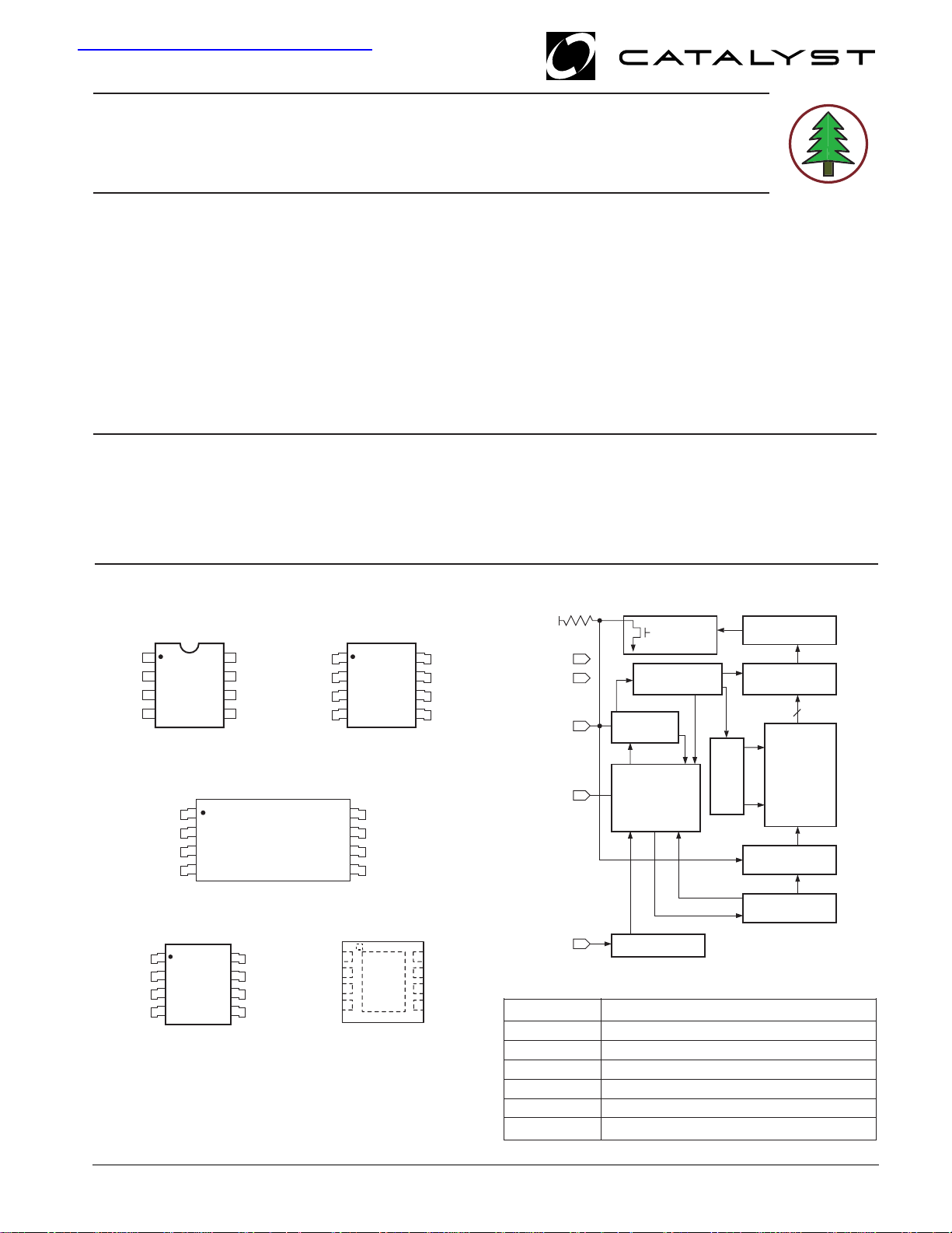
The CAT24FC16 is a 16-kb Serial CMOS EEPROM
internally organized as 2048 words of 8 bits each.
Catalyst’s advanced CMOS technology substantially
reduces device power requirements. The CAT24FC16
PIN CONFIGURATION
DIP Package (P, L)
1
NC
NC
NC
V
SS
8
2
7
3
6
4
5
V
CC
WP
SCL
SDA
SOIC Package (J, W)
1
NC
NC
NC
V
SS
8
2
7
3
6
4
5
V
CC
WP
SCL
SDA
L
E
A
E
E
R
D
F
■ 1,000,000 program/erase cycles
■ 100 year data retention
■ 8-pin DIP, 8-pin SOIC, 8-pin TSSOP, 8-pin MSOP
and TDFN packages
- “Green” package option available
■ 256 x 8 memory organization
■ Hardware write protect
features a 16-byte page write buffer. The device operates
via the I
2
C bus serial interface and is available in 8-pin
DIP, 8-pin SOIC, 8-pin TSSOP, 8-pin MSOP and TDFN
packages.
BLOCK DIAGRAM
EXTERNAL LOAD
SENSE AMPS
SHIFT REGISTERS
COLUMN
DECODERS
V
CC
V
SS
SDA
D
OUT
ACK
WORD ADDRESS
BUFFERS
START/STOP
LOGIC
TM
TSSOP Package (U, Y)
8
V
CC
7
WP
6
SCL
5
SDA
TDFN Package (RD4, ZD4)
V
1
CC
WP
2
SCL
3
SDA
4
SS
1
2
3
4
NC
NC
NC
V
MSOP Package (R, Z)
1
8
NC
2
NC
3
NC
SS
4
V
* Catalyst Semiconductor is licensed by Philips Corporation
to carry the I2C Bus Protocol.
© 2004 by Catalyst Semiconductor, Inc.
Characteristics subject to change without notice.
V
CC
7
WP
6
SCL
5
SDA
XDEC
WP
8
NC
7
NC
6
NC
5
V
S
SCL
PIN FUNCTIONS
Pin Name Function
NC No Connect
SDA Serial Data/Address
SCL Serial Clock
WP Write Protect
V
CC
V
SS
CONTROL
LOGIC
STATE COUNTERS
1.8 V to 5.5 V Power Supply
Ground
1
E2PROM
DATA IN STORAGE
HIGH VOLTAGE/
TIMING CONTROL
Doc. No. 1054, Rev. G

CAT24FC16
ABSOLUTE MAXIMUM RATINGS*
Temperature Under Bias –55°C to +125°C
Storage Temperature ....................... –65°C to +150°C
Voltage on Any Pin with
Respect to Ground
VCC with Respect to Ground ............. –2.0 V to +7.0 V
Package Power Dissipation
Capability (T
(1)
............–2.0 V to V
= 25°C) .................................. 1.0 W
A
CC
+ 2.0 V
Lead Soldering Temperature (10 seconds) ...... 300°C
Output Short Circuit Current
(2)
....................... 100 mA
*COMMENT
Stresses above those listed under “Absolute Maximum Ratings” may
cause permanent damage to the device. These are stress ratings only,
and functional operation of the device at these or any other conditions
outside of those listed in the operational sections of this specification is not
implied. Exposure to any absolute maximum rating for extended periods
may affect device performance and reliability.
RELIABILITY CHARACTERISTICS
Symbol Parameter Reference Test Method Min Typ Max Units
(3)
N
V
I
LTH
T
END
DR
ZAP
(3)
(3)
(3)(4)
Endurance MIL-STD-883, Test Method 1033 1,000,000 Cycles/Byte
Data Retention MIL-STD-883, Test Method 1008 100 Years
ESD Susceptibility MIL-STD-883, Test Method 3015 4000 Volts
Latch-up JEDEC Standard 17 100 mA
D.C. OPERATING CHARACTERISTICS
VCC = 1.8 V to 5.5 V, unless otherwise specified.
Symbol Parameter Test Conditions Min Typ Max Units
I
CC
I
CC
(5)
I
SB
I
LI
I
LO
V
IL
V
IH
V
OL1
V
OL2
Power Supply Current (Read) f
Power Supply Current (Write) f
Standby Current (VCC = 5.0 V) VIN = GND or V
Input Leakage Current VIN = GND to V
Output Leakage Current V
Input Low Voltage –1V
= 100 kHz 1 mA
SCL
= 100 kHz 3 mA
SCL
1 µA
1 µA
1 µA
x 0.3 V
CC
= GND to V
OUT
CC
CC
CC
Input High Voltage VCC x 0.7 VCC + 1.0 V
Output Low Voltage (VCC = 3.0 V) IOL = 3 mA 0.4 V
Output Low Voltage (VCC = 1.8 V) IOL = 1.5 mA 0.5 V
CAPACITANCE TA = 25°C, f = 400 kHz, VCC = 5 V
Symbol Test Conditions Min Typ Max Units
(3)
C
I/O
(3)
C
IN
Note:
(1) The minimum DC input voltage is –0.5 V. During transitions, inputs may undershoot to –2.0 V for periods of less than 20 ns. Maximum DC
voltage on output pins is VCC + 0.5 V, which may overshoot to VCC + 2.0 V for periods of less than 20 ns.
(2) Output shorted for no more than one second. No more than one output shorted at a time.
(3) This parameter is tested initially and after a design or process change that affects the parameter.
(4) Latch-up protection is provided for stresses up to 100 mA on address and data pins from –1.0 V to VCC + 1.0 V.
(5) Maximum standby current (ISB) = 10µA for the Extended Automotive temperature range.
Input/Output Capacitance (SDA) V
Input Capacitance (other pins) V
= 0 V 8 pF
I/O
= 0 V 6 pF
IN
Doc. No. 1054, Rev. G
2
A.C. CHARACTERISTICS
VCC = 1.8 V to 5.5 V, unless otherwise specified.
Read & Write Cycle Limits
Symbol Parameter 1.8 V - 5.5 V 2.5 V - 5.5 V
Min Max Min Max Units
CAT24FC16
F
SCL
(1)
T
I
t
AA
t
BUF
t
HD:STA
t
LOW
t
HIGH
t
SU:STA
t
HD:DAT
t
SU:DAT
(1)
t
R
(1)
t
F
t
SU:STO
t
DH
(1)
Clock Frequency 100 400 kHz
Noise Suppression Time 100 100 ns
Constant at SCL, SDA Inputs
SCL Low to SDA Data Out 3.5 0.9 µs
and ACK Out
Time the Bus Must be Free Before 4.7 1.3 µs
a New Transmission Can Start
Start Condition Hold Time 4 0.6 µs
Clock Low Period 4.7 1.3 µs
Clock High Period 4 0.6 µs
Start Condition Setup Time 4.7 0.6 µs
(for a Repeated Start Condition)
Data In Hold Time 0 0 ns
Data In Setup Time 250 100 ns
SDA and SCL Rise Time 1 0.3 µs
SDA and SCL Fall Time 300 300 ns
Stop Condition Setup Time 4 0.6 µs
Data Out Hold Time 100 100 ns
Power-Up Timing
(1)(2)
Symbol Parameter Min Typ Max Units
t
PUR
t
PUW
Power-up to Read Operation 1 ms
Power-up to Write Operation 1 ms
Write Cycle Limits
Symbol Parameter Min Typ Max Units
t
WR
The write cycle time is the time from a valid stop
condition of a write sequence to the end of the internal
program/erase cycle. During the write cycle, the bus
Note:
(1) This parameter is tested initially and after a design or process change that affects the parameter.
(2) t
PUR
and t
are the delays required from the time VCC is stable until the specified operation can be initiated.
PUW
Write Cycle Time 5 ms
interface circuits are disabled, SDA is allowed to remain
high, and the device does not respond to its slave
address.
3
Doc No. 1054, Rev. G
CAT24FC16
FUNCTIONAL DESCRIPTION
The CAT24FC16 supports the I2C Bus data transmission
protocol. This Inter-Integrated Circuit Bus protocol defines
any device that sends data to the bus to be a transmitter
and any device receiving data to be a receiver. Data
transfer is controlled by the Master device which
generates the serial clock and all START and STOP
conditions for bus access. The CAT24FC16 operates as
a Slave device. Both the Master and Slave devices can
operate as either transmitter or receiver, but the Master
device controls which mode is activated.
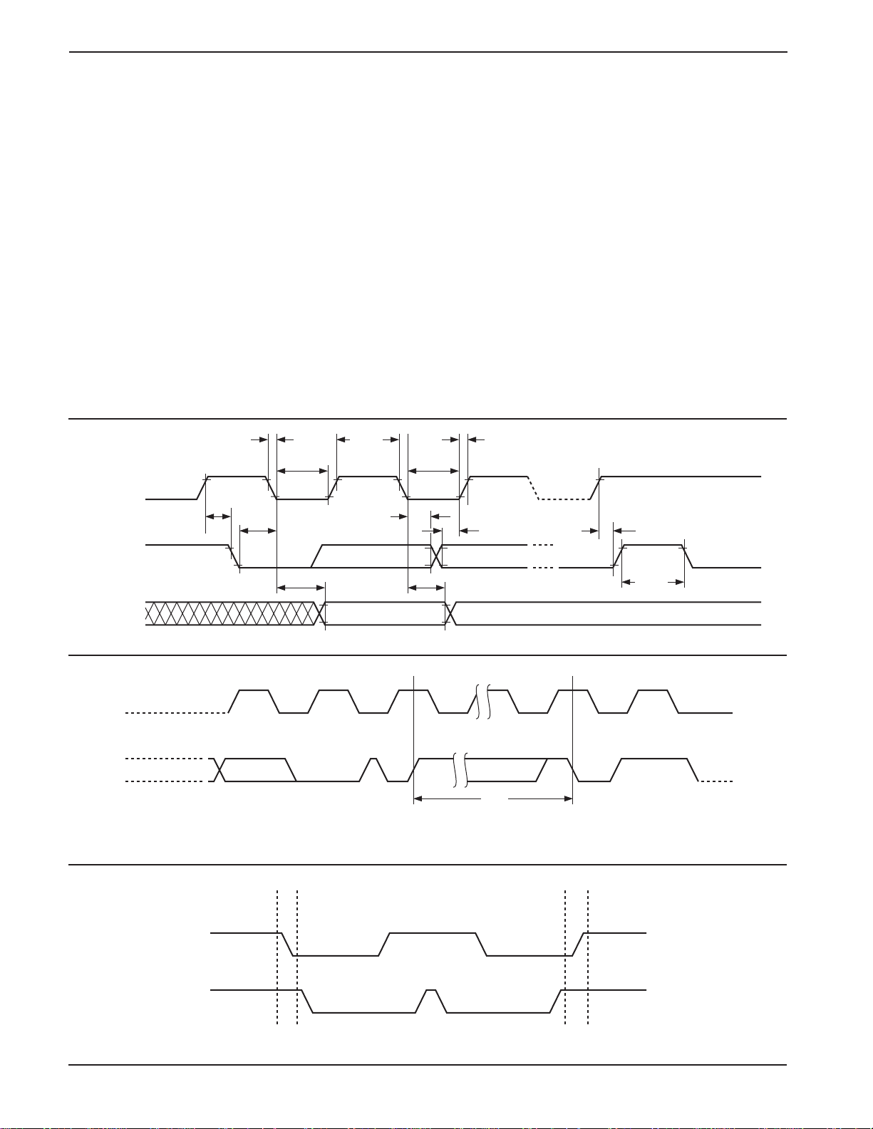
Figure 1. Bus Timing
SCL
t
SU:STA
t
F
t
LOW
t
HD:STA
t
HIGH
t
HD:DAT
PIN DESCRIPTIONS
SCL: Serial Clock
The CAT24FC16 serial clock input pin is used to clock all
data transfers into or out of the device. This is an input
pin.
SDA: Serial Data/Address
The CAT24FC16 bidirectional serial data/address pin is
used to transfer data into and out of the device. The SDA
pin is an open drain output and can be wire-ORed with
other open drain or open collector outputs.
WP: Write Protect
This input, when tied to GND, allows write operations to
the entire memory. For CAT24FC16 when this pin is tied
to VCC, the entire array of memory is write protected.
When left floating, memory is unprotected.
t
R
t
LOW
t
SU:DAT
t
SU:STO
SDA IN
SDA OUT
Figure 2. Write Cycle Timing
SCL
SDA
BYTE n
Figure 3. Start/Stop Timing
SDA
t
t
AA
ACK8TH BIT
STOP
CONDITION
t
DH
t
WR
START
CONDITION
BUF
ADDRESS
Doc. No. 1054, Rev. G
SCL
START BIT
STOP BIT
4
 Loading...