

Page 1
CAT5113
ONE
OF
ONE HUNDRED
DECODER
99
98
97
28
2
1
0
TRANSFER
GATES
RESISTOR
ARRAY
R
H
L
R
H
V
V
L
/
/
V
WRW
/
7-BIT
NONVOLATILE
MEMORY
STORE AND
RECALL
CONTROL
CIRCUITRY
U/D
INC
CS
Vcc
V
SS
7-BIT
UP/DOWN
COUNTER
N
E
G
F
O
R
L
A
H
E
E
100-Tap Digitally Programmable Potentiometer (DPP™)
FEATURES
■ 100-position linear taper potentiometer
■ Non-volatile EEPROM wiper storage
■ 10nA ultra-low standby current
■ Single supply operation: 2.5V-6.0V
■ Increment Up/Down serial interface
ΩΩ
■ Resistance values: 1k
Ω ,10k
ΩΩ
ΩΩ
Ω , 50k
ΩΩ
■ Available in PDIP, SOIC, TSSOP and MSOP packages
Ω Ω
Ω and 100k
Ω Ω
ΩΩ
Ω
ΩΩ
APPLICATIONS
■ Automated product calibration
■ Remote control adjustments
■ Offset, gain and zero control
■ Tamper-proof calibrations
■ Contrast, brightness and volume controls
■ Motor controls and feedback systems
■ Programmable analog functions
DESCRIPTION
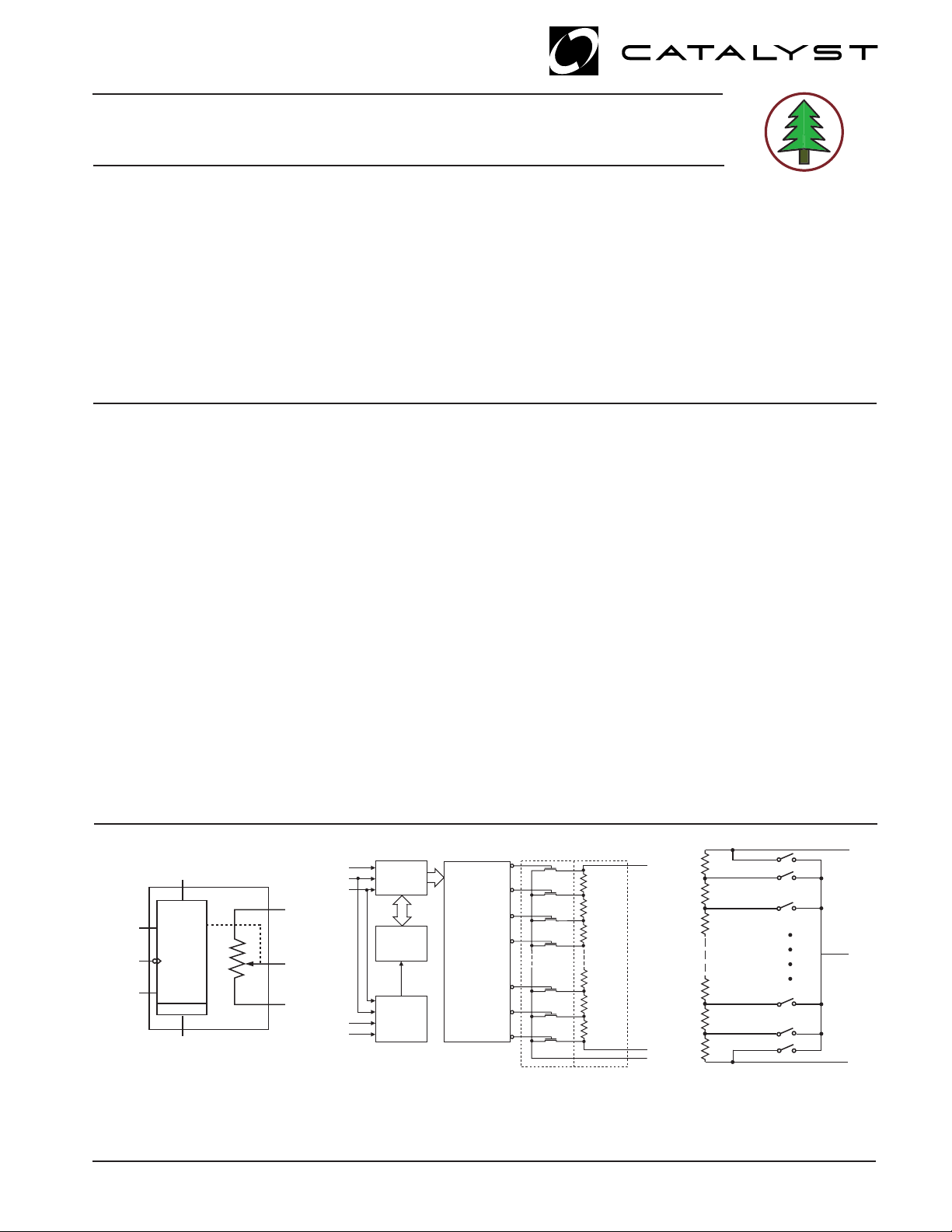
The CAT5113 is a single digitally programmable
potentiometer (DPP™) designed as a electronic
replacement for mechanical potentiometers and trim
pots. Ideal for automated adjustments on high volume
production lines, they are also well suited for
applications where equipment requiring periodic
adjustment is either difficult to access or located in a
hazardous or remote environment.
new system values without effecting the stored
setting. Wiper-control of the CAT5113 is
accomplished with three input control pins, CS, U/D,
and INC. The INC input increments the wiper in the
direction which is determined by the logic state of
the U/D input. The CS input is used to select the
device and also store the wiper position prior to
power down.
L
E
A
E
E
TM
R
D
F
The CAT5113 contains a 100-tap series resistor array
connected between two terminals RH and RL. An up/
down counter and decoder that are controlled by three
input pins, determines which tap is connected to the
wiper, RW. The wiper setting, stored in nonvolatile
memory, is not lost when the device is powered
The digitally programmable potentiometer can be
used as a three-terminal resistive divider or as a
two-terminal variable resistor. DPPs bring variability and
programmability to a wide variety of applications
including control, parameter adjustments, and
signal processing.
down and is automatically reinstated when power
is returned. The wiper can be adjusted to test
FUNCTIONAL DIAGRAM
(Supply Voltage)
Vcc
R
V
/
H
H
/
V
R
W
W
/
V
R
L
L
DETAILED
1
ELECTRONIC POTENTIOMETER
IMPLEMENTATION
Doc. No. 2009, Rev. R
UP/DOWN
(U/D)
INCREMENT
(INC)
DEVICE SELECT
© 2005 by Catalyst Semiconductor, Inc.
Characteristics subject to change without notice
(CS)
Control
and
Memory
POR
GND
GENERAL
GENERAL
/
R
V
H
H
R
/
V
W
W
/
R
V
L
L
Page 2
CAT5113
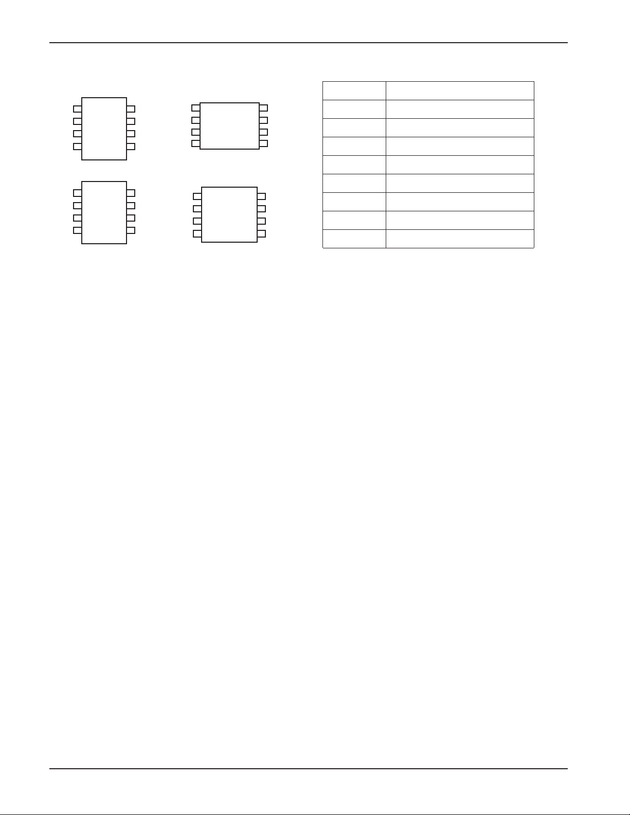
PIN CONFIGURATION
DIP Package (P, L)
INC
U/D
R
GND
1
2
3
H
4
8
7
6
5
SOIC Package (S, V)
INC
U/D
R
GND
1
2
3
H
4
8
7
6
5
V
CS
R
R
V
CS
R
R
CC
L
W
CC
L
W
TSSOP Package (U, Y)
1
CS
V
CC
INC
U/D
2
3
4
MSOP Package (R, Z)
1
INC
2
U/D
3
R
H
GND
4
8
R
L
7
R
W
6
GND
5
R
H
8
V
CC
7
CS
6
R
L
5
R
W
PIN DESCRIPTIONS
INCINC
INC: Increment Control Input
INCINC
The INC input moves the wiper in the up or down direction
determined by the condition of the U/D input.
DD
U/
D: Up/Down Control Input
DD
The U/D input controls the direction of the wiper
movement. When in a high state and CS is low, any highto-low transition on INC will cause the wiper to move one
increment toward the R
and CS is low, any high-to-low transition on INC will
cause the wiper to move one increment towards the
RL terminal.
R
High End Potentiometer Terminal
H:
RH is the high end terminal of the potentiometer. It is not
required that this terminal be connected to a potential
greater than the RL terminal. Voltage applied to the R
terminal cannot exceed the supply voltage, VCC or go
below ground, GND.
RW: Wiper Potentiometer Terminal
RW is the wiper terminal of the potentiometer. Its position
on the resistor array is controlled by the control inputs, INC,
U/D and CS. Voltage applied to the RW terminal cannot
exceed the supply voltage, V
RL: Low End Potentiometer Terminal
RL is the low end terminal of the potentiometer. It is not
required that this terminal be connected to a potential
less than the RH terminal. Voltage applied to the R
terminal cannot exceed the supply voltage, VCC or go
below ground, GND. RL and RH are electrically
interchangeable.
CSCS
CS: Chip Select
CSCS
The chip select input is used to activate the control input
terminal. When in a low state
H
or go below ground, GND.
CC
PIN FUNCTIONS
Pin Name Function
INC Increment Control
U/D Up/Down Control
R
H
Potentiometer High Terminal
GND Ground
R
W
R
L
Potentiometer Wiper Terminal
Potentiometer Low Terminal
CS Chip Select
V
CC
Supply Voltage
of the CAT5113 and is active low. When in a high
state, activity on the INC and U/D inputs will not
affect or change the position of the wiper.
DEVICE OPERATION
The CAT5113 operates like a digitally controlled
potentiometer with RH and RL equivalent to the high
and low terminals and RW equivalent to the mechanical
potentiometer's wiper. There are 100 available tap
positions including the resistor end points, RH and RL.
There are 99 resistor elements connected in series
between the RH and RL terminals. The wiper terminal is
connected to one of the 100 taps and controlled by three
inputs, INC, U/D and CS. These inputs control a sevenbit up/down counter whose output is decoded to select
the wiper position. The selected wiper position can be
stored in nonvolatile memory using the INC and
H
CS inputs.
With CS set LOW the CAT5113 is selected and will
respond to the U/D and INC inputs. HIGH to LOW
transitions on INC wil increment or decrement the
wiper (depending on the state of the U/D input and
seven-bit counter). The wiper, when at either fixed
terminal, acts like its mechanical equivalent and does
not move beyond the last position. The value of the
counter is stored in nonvolatile memory whenever CS
transitions HIGH while the INC input is also HIGH. When
the CAT5113 is powered-down, the last stored wiper
counter position is maintained in the nonvolatile memory.
When power is restored, the contents of the memory are
L
recalled and the counter is set to the value stored.
With INC set low, the CAT5113 may be de-selected
and powered down without storing the current wiper
position in nonvolatile memory. This allows the
system to always power up to a preset value stored
in nonvolatile memory.
Doc. No. 2009, Rev. R
2
Page 3
CAT5113
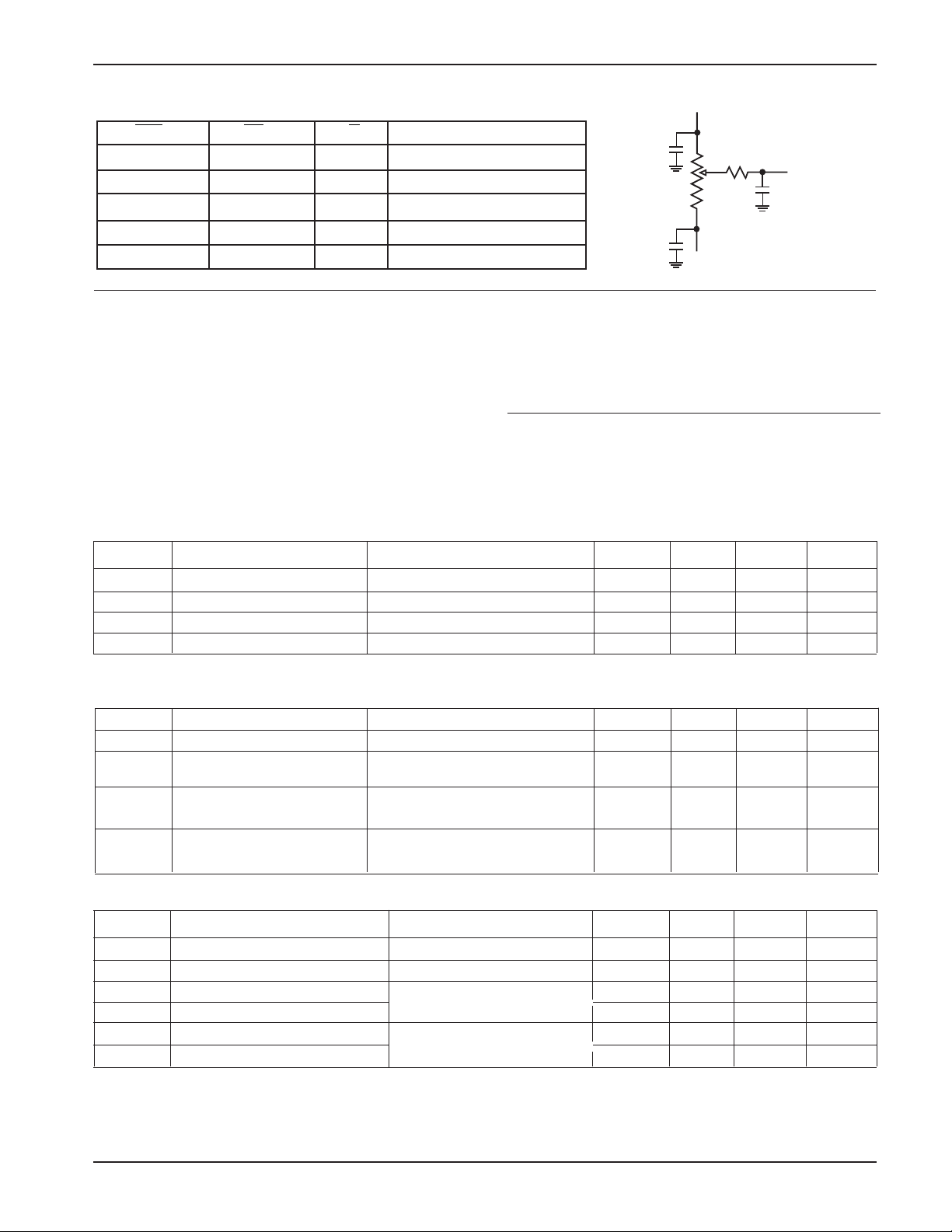
OPERATION MODES
INC CS U/D Operation
High to Low Low High Wiper toward H
High to Low Low Low Wiper toward L
High Low to High X Store Wiper Position
Low Low to High X No Store, Return to Standby
X High X Standby
ABSOLUTE MAXIMUM RATINGS
Supply Voltage
VCC to GND ...................................... –0.5V to +7V
Inputs
CS to GND .............................–0.5V to V
INC to GND ............................ –0.5V to V
U/D to GND ............................ –0.5V to V
H to GND ................................ –0.5V to V
L to GND ................................ –0.5V to V
W to GND ............................... –0.5V to V
RELIABILITY CHARACTERISTICS
CC
CC
CC
CC
CC
CC
+0.5V
+0.5V
+0.5V
+0.5V
+0.5V
+0.5V
Operating Ambient Temperature
Commercial (‘C’ or Blank suffix) ...... 0°C to +70°C
Industrial (‘I’ suffix) ...................... – 40°C to +85°C
Junction Temperature ..................................... +150°C
Storage Temperature ....................... –65°C to +150°C
Lead Soldering (10 sec max) .......................... +300°C
* Stresses above those listed under Absolute Maximum Ratings may
cause permanent damage to the device. Absolute Maximum Ratings
are limited values applied individually while other parameters are
within specified operating conditions, and functional operation at any
of these conditions is NOT implied. Device performance and reliability
may be impaired by exposure to absolute rating conditions for extended
periods of time.
R
H
C
H
C
L
R
wi
R
WB
C
W
Potentiometer
R
L
Equivalent Circuit
Symbol Parameter Test Method Min Typ Max Units
(1)
V
I
T
N
ZAP
LTH
DR
END
(1)(2)
ESD Susceptibility MIL-STD-883, Test Method 3015 2000 Volts
Latch-Up JEDEC Standard 17 100 mA
Data Retention MIL-STD-883, Test Method 1008 100 Years
Endurance MIL-STD-883, Test Method 1003 1,000,000 Stores
DC Electrical Characteristics: VCC = +2.5V to +6.0V unless otherwise specified
Power Supply
Symbol Parameter Conditions Min Typ Max Units
V
CC
I
CC1
I
CC2
ISB
(2)
1
Operating Voltage Range 2.5 6.0 V
Supply Current (Increment) VCC = 6V, f = 1MHz, IW=0 100 µA
= 6V, f = 250kHz, IW=0 50
V
CC
Supply Current (Write) Programming, VCC = 6V 1 mA
VCC = 3V 500 µA
Supply Current (Standby) CS=VCC-0.3V 0.01 1 µA
U/D, INC=VCC-0.3V or GND
Logic Inputs
Symbol Parameter Conditions Min Typ Max Units
I
IH
I
IL
V
IH1
V
IL1
V
IH2
V
IL2
NOTES: (1) This parameter is tested initially and after a design or process change that affects the parameter.
Input Leakage Current VIN = V
CC
10 µA
Input Leakage Current VIN = 0V –10 µA
TTL High Level Input Voltage 4.5V ≤ VCC ≤ 5.5V 2 V
CC
TTL Low Level Input Voltage 0 0.8 V
CMOS High Level Input Voltage 2.5V ≤ VCC ≤ 6V VCC x 0.7 VCC + 0.3 V
CMOS Low Level Input Voltage -0.3 VCC x 0.2 V
(2) Latch-up protection is provided for stresses up to 100mA on address and data pins from –1V to VCC + 1V
(3) IW=source or sink
(4) These parameters are periodically sampled and are not 100% tested.
V
3
Doc. No. 2009, Rev. R
Page 4

CAT5113
Potentiometer Parameters
Symbol Parameter Conditions Min Typ Max Units
R
POT
Potentiometer Resistance -01 Device 1
-50 Device 50 kΩ
-50 Device 50
-00 Device 100
Pot Resistance Tolerance ±20 %
V
V
RH
RL
Voltage on RH pin 0 V
Voltage on RL pin 0 V
CC
CC
V
V
Resolution 1% %
INL Integral Linearity Error IW ≤ 2µA 0.5 1 LSB
DNL Differential Linearity Error IW ≤ 2µA 0.25 0.5 LSB
R
Wi
Wiper Resistance VCC = 5V, IW = 1mA 400 Ω
VCC = 2.5V, IW = 1mA 1 kΩ
I
W
TC
RPOT
TC
RATIO
V
CH/CL/CW
N
Wiper Current (1) -4.4 4.4 mA
TC of Pot Resistance 300 ppm/oC
Ratiometric TC 20 ppm/oC
Noise 100kHz / 1kHz 8/24 nV/ H
Potentiometer Capacitances 8/8/25 pF
fc Frequency Response Passive Attenuator, 10kΩ 1.7 MHz
Note:
1. This parameter is not 100% tested.
z
Doc. No. 2009, Rev. R
4
Page 5
AC CONDITIONS OF TEST
VCC Range 2.5V ≤ VCC ≤ 6V
CAT5113
Input Pulse Levels 0.2VCC to 0.7V
CC
Input Rise and Fall Times 10ns
Input Reference Levels 0.5V
CC
AC OPERATING CHARACTERISTICS:
VCC = +2.5V to +6.0V, VH = VCC, VL = 0V, unless otherwise specified
Symbol Parameter Min Typ
t
CI
t
DI
t
ID
t
IL
t
IH
t
IC
t
CPH
t
CPH
t
IW
t
CYC
t
R, tF
t
PU
t
WR
(2)
(2)
CS to INC Setup 100 ——ns
U/D to INC Setup 50 ——ns
U/D to INC Hold 100 ——ns
INC LOW Period 250 ——ns
INC HIGH Period 250 ——ns
INC Inactive to CS Inactive 1 ——µs
CS Deselect Time (NO STORE) 100 ——ns
CS Deselect Time (STORE) 10 ——ms
INC to V
Change — 15µs
OUT
INC Cycle Time 1 ——µs
INC Input Rise and Fall Time —— 500 µs
Power-up to Wiper Stable —— 1 msec
Store Cycle — 510ms
(1)
Max Units
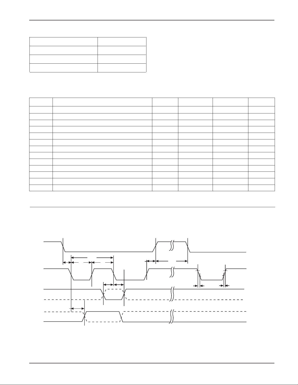
A. C. TIMING
CS
t
t
CI
CYC
t
IL
t
IH
t
IC
INC
tID
tDI
U/D
t
IW
R
W
(1) Typical values are for TA=25˚C and nominal supply voltage.
(2) This parameter is periodically sampled and not 100% tested.
(3) MI in the A.C. Timing diagram refers to the minimum incremental change in the W output due to a change in the wiper position.
(store)
t
CPH
90% 90%
t
F
10%
t
R
(3)
MI
5
Doc. No. 2009, Rev. R
Page 6
CAT5113
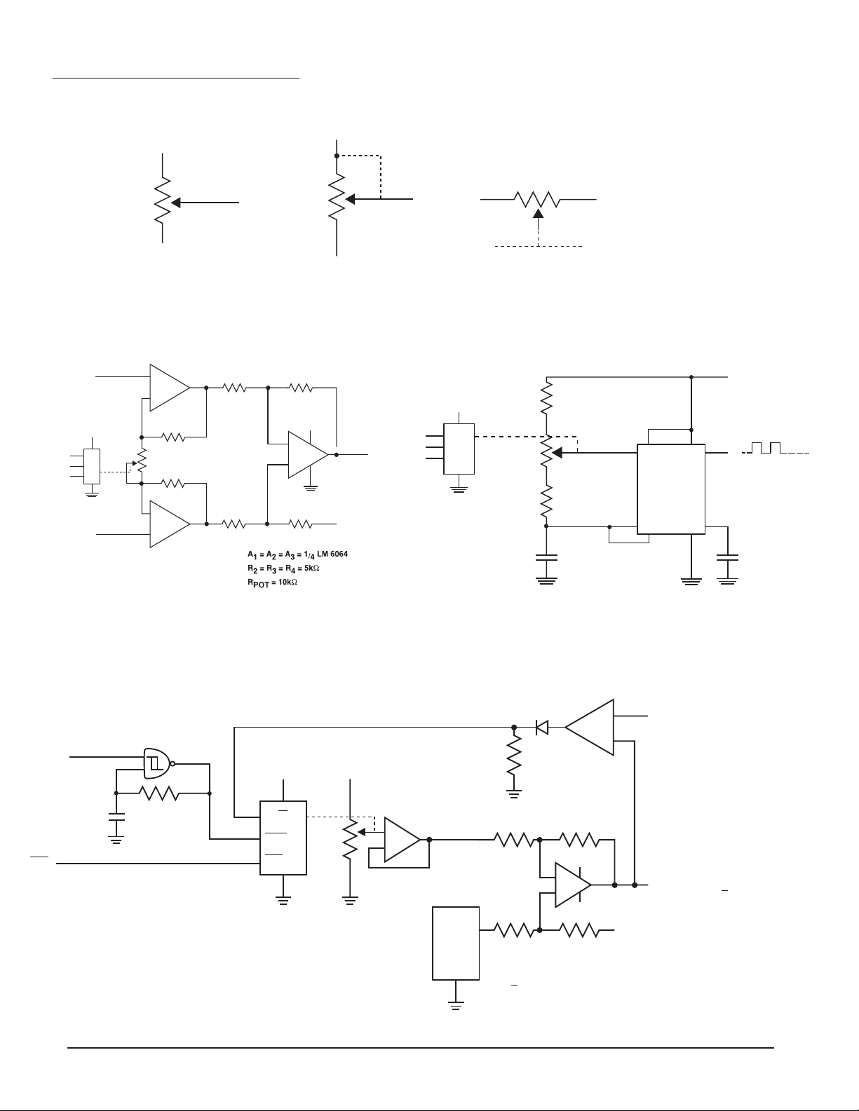
APPLICATIONS INFORMATION
Potentiometer Configurations
(a) resistive divider (b) variable resistance (c) two-port
Applications
A
3
V
1
(-)
+5V
DPP
U/
CAT5114/5113
V
2
(+)
1
+
–
2
R
2
R
1
R
2
6
A
2
–
+
5
R
1
7
3
9
10
R
3
–
+
R
R
4
+5V
4
+5V
+5V
8
A
3
4
11
8
+2.5V
V
O
2
U/
1
7
4
R
R
A
B
.01 F,
.003 F
R
{
R
{
C
1
6
}
pR
POT
5
(1-p)R
}
3
POT
4
7
2
6
8
3
555
5
21
.01 F
OSC
CS
Programmable Instrumentation Amplifier Programmable Sq. Wave Oscillator (555)
ICIB
4
11
1
6
–
+
1.00V = V
5
V
ICIA
100mV = V
= 1V + 1mV
OUT
SHIFT
REF
IC3A
1/4 74HC132
10k
0.01 F
+5V +200mV
U/D
INC
CS
CAT5112/5111
IC2
7
20k
V
+
–
CORR
499k
Sensor
499k
499k
+5V
2
–
+
3
-5V
499k
1V + 50mV
V
SENSR
Doc. No. 2009, Rev. R
Sensor Auto Referencing Circuit
6
Page 7
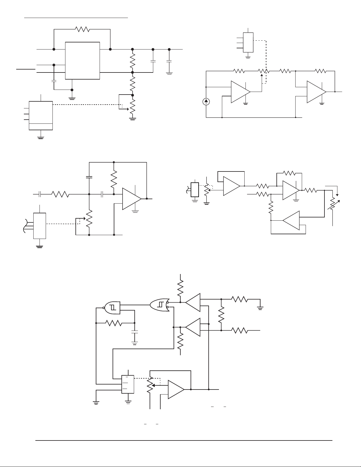
APPLICATIONS INFORMATION
100k
V
OUT
SD
GND
2952
FB
VIN (UNREG)
SHUTDOWN
2
U/
1
7
+5V
8
Control
and
Memory
POR
4
1F
CAT5114/5113
1.23V
CAT5113
+5V
8
2
U/
V0 (REG)
R1
11k
.1
R2
820
3
5
R3
10k
6
6.8 F
–
+
I
S
3
CAT5114/5113
1
7
4
+5V
pR (1-p)R
}
}
6
3
5
7
10k
6
A1
4
LT1097
22
3
+2.5V
1M330330
+5V
–
7
6
V
O
A2
4
+
Programmable Voltage Regulator
C1
1F
V
S
+5V
R1
50k
CAT5114/5113
.001
R2
10k
C2
.001
R3
100k
2
3
–
+
+2.5V
+5V
7
6
V
O
4
A1
Serial
Bus
Programmable I to V convertor
CAT5112/5111
+5V
+5V
–
+
+2.5V
R1
100k
V
S
R1
100k
100k
R1
100k
+5V
2
–
3
+
R1
7
A2
R
2.5k
4
1
11
+
5
–
6
I
S
+2.5V
A1=A2=1/4 LMC6064A
Programmable Bandpass Filter Programmable Current Source/Sink
+5V
CHI
–
+
–
+
IC1
393
2
3
6
5
R
V
LL
1
R
2
R
3
+5V
V
UL
OSC
10k
IC2
74HC132
1
CLO
7
0.1 F
IC3
CAT5114/5113
+5V
8
2
U/D
1
INC
7
CS
6
10k
4
5
3
V
+2.5V
S
0 < VS < 2.5V
Automatic Gain Control
+5V
–
+
AI
IC4
2.5V < VO < 5V
7
V
O
Doc. No. 2009, Rev. R
Page 8
CAT5113
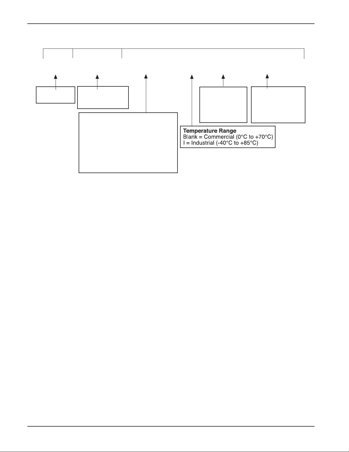
ORDERING INFORMATION
Prefix Device # Suffix
CAT
Optional
Company ID
5113
Product Number
5111: Buffered
5113: Unbuffered
Package
P: PDIP
S
I
-10
Resistance
-01: 1kohms
-10: 10kohms
-50: 50kohms
-00: 100kohms
TE13
Tape & Reel
TE13
SOIC: 2000/Reel
TSSOP: 2000/Reel
MSOP: 2500/Reel
S: SOIC
U: TSSOP
R:
MSOP
L: PDIP (Lead free, Halogen free)
V: SOIC (Lead free, Halogen free)
Y: TSSOP (Lead free, Halogen free)
Z: MSOP (Lead free, Halogen free)
Notes:
(1) The device used in the above example is a CAT5113 SI-10TE13 (SOIC, 10K Ohms, Industrial Temperature, Tape & Reel)
Doc. No. 2009, Rev. R
8
Page 9
REVISION HISTORY
Date Rev. Reason
10/9/2003 M Revised Features
Revised DC Electrical Characteristics
3/10/2004 N Updated Potentiometer Parameters
3/29/2004 O Changed Green Package marking for SOIC from W to V
4/02/2004 P Add 1KW version to data sheet
4/8/2004 Q Eliminated data sheet designation
Updated Tape and Reel specs in Ordering Information
1/25/2005 R Updated Potentiometer Parameters
Copyrights, Trademarks and Patents
Trademarks and registered trademarks of Catalyst Semiconductor include each of the following:
DPP ™ AE2 ™
CAT5113
Catalyst Semiconductor has been issued U.S. and foreign patents and has patent applications pending that protect its products. For a complete list of patents
issued to Catalyst Semiconductor contact the Company’s corporate office at 408.542.1000.
CATALYST SEMICONDUCTOR MAKES NO WARRANTY, REPRESENTATION OR GUARANTEE, EXPRESS OR IMPLIED, REGARDING THE SUITABILITY OF ITS
PRODUCTS FOR ANY PARTICULAR PURPOSE, NOR THAT THE USE OF ITS PRODUCTS WILL NOT INFRINGE ITS INTELLECTUAL PROPERTY RIGHTS OR THE
RIGHTS OF THIRD PARTIES WITH RESPECT TO ANY PARTICULAR USE OR APPLICATION AND SPECIFICALLY DISCLAIMS ANY AND ALL LIABILITY ARISING
OUT OF ANY SUCH USE OR APPLICATION, INCLUDING BUT NOT LIMITED TO, CONSEQUENTIAL OR INCIDENTAL DAMAGES.
Catalyst Semiconductor products are not designed, intended, or authorized for use as components in systems intended for surgical implant into the body, or
other applications intended to support or sustain life, or for any other application in which the failure of the Catalyst Semiconductor product could create a
situation where personal injury or death may occur.
Catalyst Semiconductor reserves the right to make changes to or discontinue any product or service described herein without notice. Products with data sheets
labeled "Advance Information" or "Preliminary" and other products described herein may not be in production or offered for sale.
Catalyst Semiconductor advises customers to obtain the current version of the relevant product information before placing orders. Circuit diagrams illustrate
typical semiconductor applications and may not be complete.
Catalyst Semiconductor, Inc.
Corporate Headquarters
1250 Borregas Avenue
Sunnyvale, CA 94089
Phone: 408.542.1000
Fax: 408.542.1200
www.catsemi.com
Publication #: 2009
Revison: R
Issue date: 1/25/04
9
Doc. No. 2009, Rev. R
 Loading...