

Page 1
T
T
查询CAT1024JE-25TE13供应商
Preliminary Information
CAT1024, CAT1025
Supervisory Circuits with I2C Serial 2k-bit CMOS EEPROM and Manual Reset
FEATURES
■ Precision power supply voltage monitor
— 5V, 3.3V and 3V systems
— Five threshold voltage options
■ Active high or low reset
— Valid reset guaranteed at V
■ 400kHz I
2
C bus
CC
= 1V
■ 3.0V to 5.5V operation
■ Low power CMOS technology
DESCRIPTION
The CAT1024 and CAT1025 are complete memory and
supervisory solutions for microcontroller-based systems.
A 2k-bit serial EEPROM memory and a system power
supervisor with brown-out protection are integrated
together in low power CMOS technology. Memory
interface is via a 400kHz I2C bus.
The CAT1025 provides a precision VCC sense circuit
and two open drain outputs: one (RESET) drives high
and the other (RESET) drives low whenever VCC falls
below the reset threshold voltage. The CAT1025 also
has a Write Protect input (WP). Write operations are
disabled if WP is connected to a logic high.
The CAT1024 also provides a precision VCC sense
circuit, but has only a RESET output and does not have
a Write Protect input.
The power supply monitor and reset circuit protect
memory and system controllers during power up/down
and against brownout conditions. Five reset threshold
■ 16-Byte page write buffer
■ Built-in inadvertent write protection
— WP pin (CAT1025)
■ 1,000,000 Program/Erase cycles
■ Manual reset input
■ 100 year data retention
■ 8-pin DIP, SOIC, TSSOP, MSOP &
TDFN (3x3mm foot print) packages
■ Industrial and extended temperature ranges
voltages support 5V, 3.3V and 3V systems. If power supply
voltages are out of tolerance reset signals become active,
preventing the system microcontroller, ASIC or peripherals
from operating. Reset signals become inactive typically 200
ms after the supply voltage exceeds the reset threshold
level. With both active high and low reset signals, interface
to microcontrollers and other ICs is simple. In addition, the
RESET pin or a separate input, MR, can be used as an input
for push-button manual reset capability.
The CAT1024/25 memory features a 16-byte page. In
addition, hardware data protection is provided by a V
sense circuit that prevents writes to memory whenever V
falls below the reset threshold or until VCC reaches the reset
threshold during power up.
Available packages include an 8-pin DIP, 8-pin SOIC, 8-pin
TSSOP, 8-pin TDFN and 8-pin MSOP. The TDFN package
thickness is 0.8mm maximum. TDFN footprint is 3x3mm.
N
E
G
F
O
R
L
A
H
L
E
A
E
E
E
E
TM
R
D
F
CC
CC
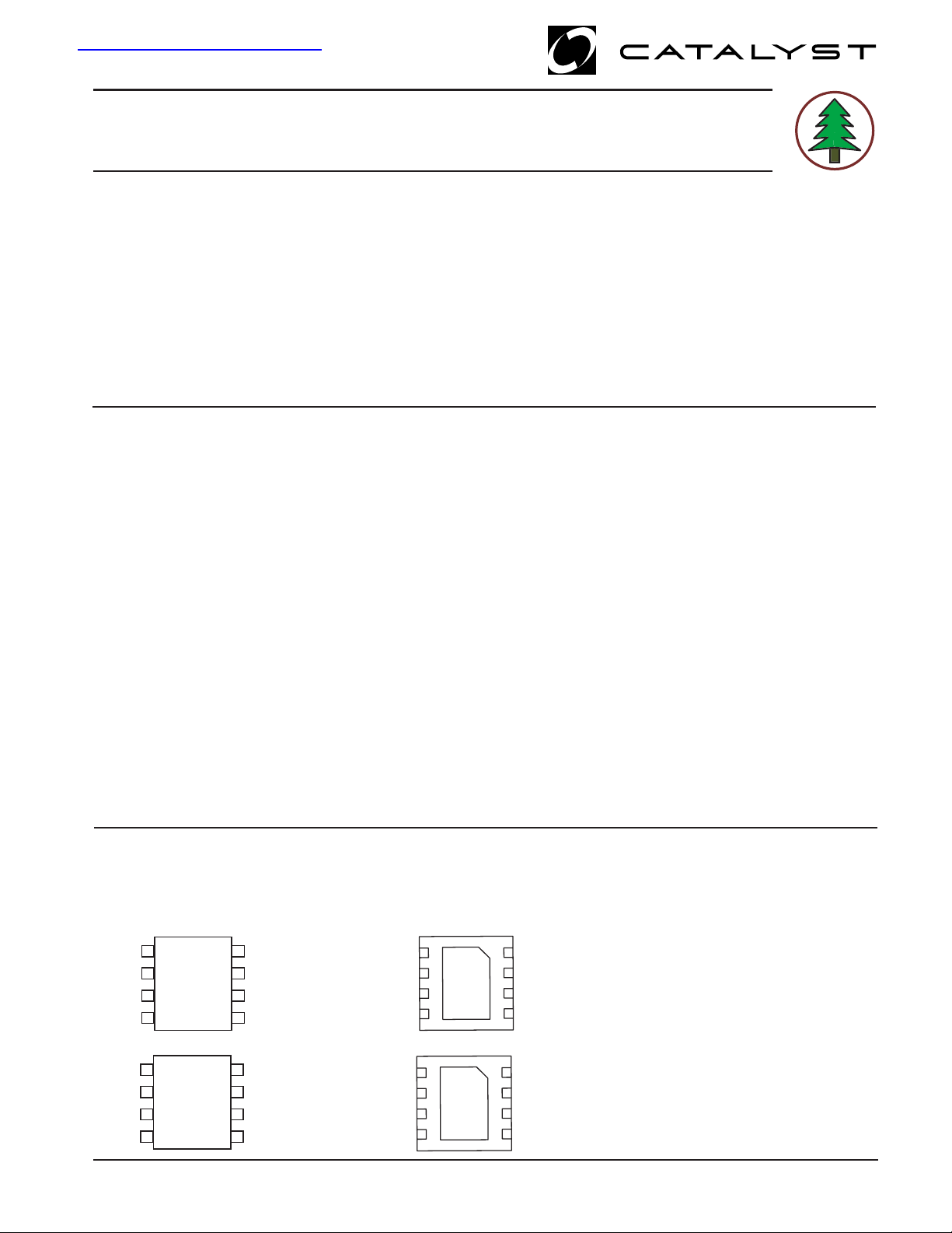
PIN CONFIGURATION
DIP Package (P, L)
SOIC Package (J, W)
TSSOP Package (U, Y)
MSOP Package (R, Z)
1
MR V
RESET
RESET
RESET
© 2004 by Catalyst Semiconductor, Inc.
Characteristics subject to change without notice
2
CAT1024
NC
3
V
4
SS
1
MR V
2
CAT1025
3
V
4
SS
8
CC
NC
7
SCL
6
SDA
5
8
V
CC
CC
WP
7
SCL
6
SDA
5
(Bottom View)
TDFN Package: 3mm x 3mm
0.8mm maximum height - (RD4, ZD4)
V
CC
NC
SCL
SDA
V
CC
WP
SCL
SDA
8
7
6
5
8
7
6
5
CAT1024
CAT1025
1
2
3
4
1
2
3
4
MR
RESE
NC
V
SS
MR
RESE
RESET
V
SS
Doc No. 3008, Rev. M
Page 2
CAT1024, CAT1025
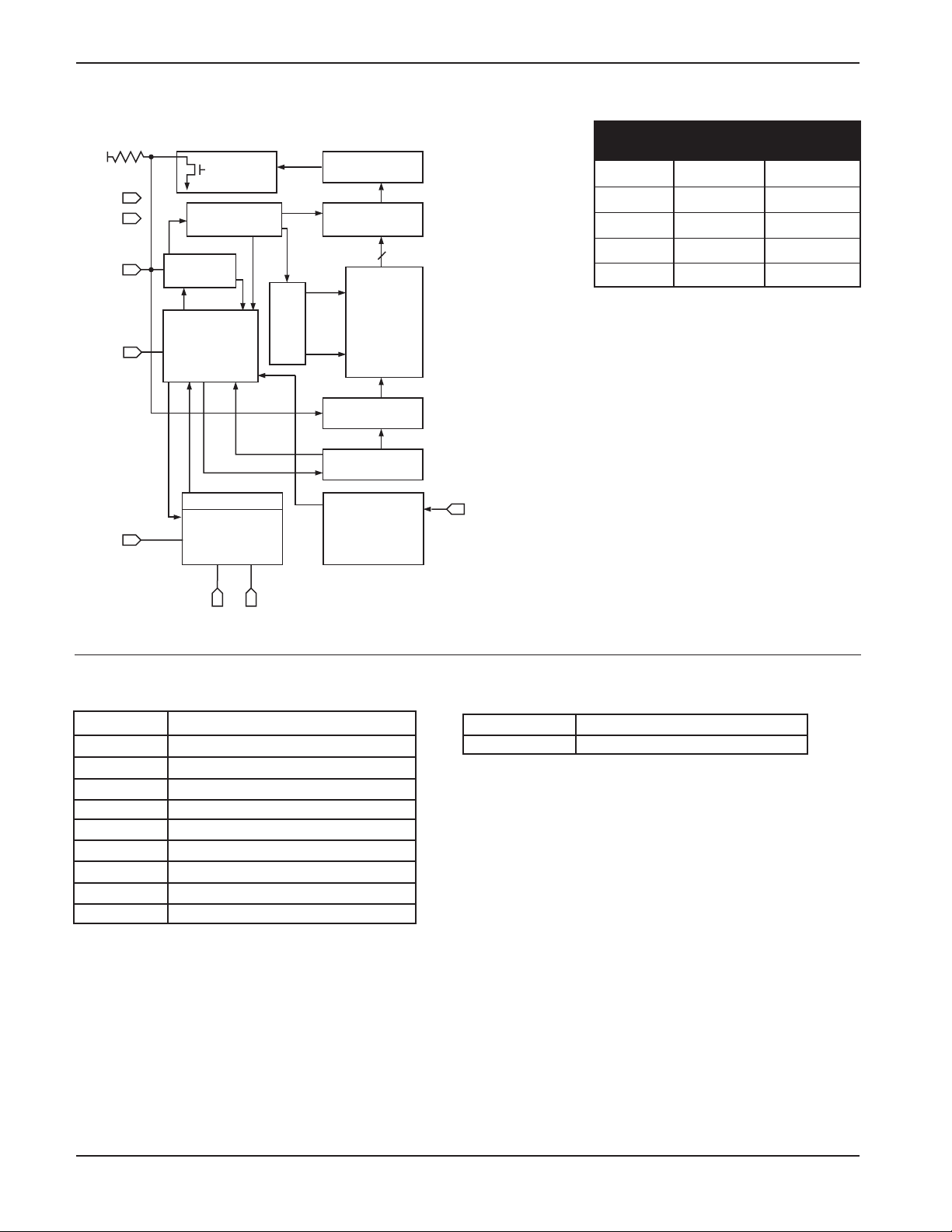
BLOCK DIAGRAM — CAT1024, CAT1025
EXTERNAL LOAD
SENSE AMPS
SHIFT REGISTERS
COLUMN
DECODERS
2kbit
EEPROM
DATA IN STORAGE
HIGH VOL T A GE/
TIMING CONTROL
STATE COUNTERS
SLAVE
ADDRESS
COMPARATORS
V
CC
V
SS
SDA
WP*
MR
D
ACK
WORD ADDRESS
BUFFERS
START/STOP
LOGIC
CONTROL
LOGIC
RESET Controller
Precision
Vcc Monitor
OUT
XDEC
Threshold Voltage Options
Part Dash Minimum Maximum
Number Threshold Threshold
-45 4.50 4.75
-42 4.25 4.50
-30 3.00 3.15
-28 2.85 3.00
-25 2.55 2.70
SCL
*
*CAT1025 Only
RESET RESET
PIN FUNCTIONS
Pin Name Function
NC No Connect
RESET Active Low Reset Input/Output
V
SS
SDA Serial Data/Address
SCL Clock Input
RESET Active High Reset Output (CAT1025 only)
V
CC
WP Write Protect (CAT1025 only)
MR Manual Reset Input
Ground
Power Supply
OPERATING TEMPERATURE RANGE
Industrial -40˚C to 85˚C
Extended -40˚C to 125˚C
Doc. No. 3008, Rev. M
2
Page 3
PIN DESCRIPTION
CAT1024, CAT1025
RESET/
RESETRESET
RESET: RESET OUTPUTS
RESETRESET
(RESET CAT1025 Only)
These are open drain pins and RESET can be used as a
manual reset trigger input. By forcing a reset condition on
the pin the device will initiate and maintain a reset condition.
The RESET pin must be connected through a pull-down
resistor, and the RESET pin must be connected through a
pull-up resistor.
SDA: SERIAL DATA ADDRESS
The bidirectional serial data/address pin is used to transfer
all data into and out of the device. The SDA pin is an open
drain output and can be wire-ORed with other open drain
or open collector outputs.
SCL: SERIAL CLOCK
Serial clock input.
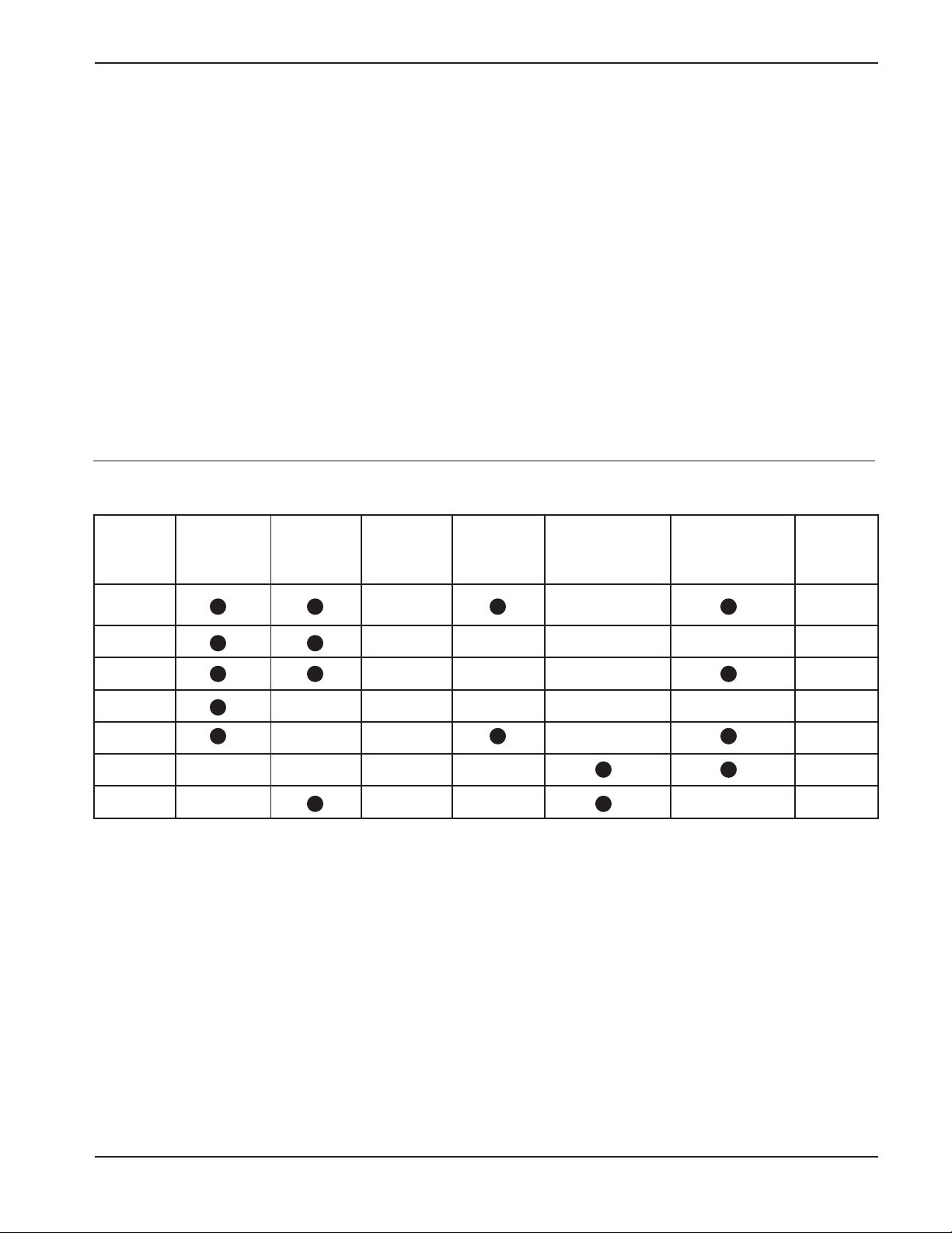
CAT10XX FAMILY OVERVIEW
launaM
eciveD
teseR
niPtupnI
godhctaW
godhctaW
rotinoM
niP
MR:MR:
MR: MANUAL RESET INPUT
MR:MR:
Manual Reset input is a debounced input that can be
connected to an external source for Manual Reset.
Pulling the MR input low will generate a Reset condition.
Reset outputs are active while MR input is low and for
the reset timeout period after MR returns to high. The
input has an internal pull-up resistor.
WP (CAT1025 Only): WRITE PROTECT INPUT
When tied to V
or left unconnected write operations
SS
to the entire array are allowed. When tied to VCC, the
entire array is protected. This input has an internal pull
down resistor.
etirW
noitcetorP
niP
tnednepednI
yrailixuA
esneSegatloV
evitcA:TESER
WOLdnahgiH
MORPEE
1201TAC ADS k2
2201TAC ADS k2
3201TAC IDW k2
4201TAC k2
5201TAC k2
6201TAC k2
7201TAC IDW k2
For supervisory circuits with embedded 16k EEPROM, please refer to the CAT1161, CAT1162 and CAT1163
data sheets.
3
Doc No. 3008, Rev. M
Page 4
CAT1024, CAT1025
ABSOLUTE MAXIMUM RATINGS
Temperature Under Bias ................. –55°C to +125°C
Storage Temperature....................... –65°C to +150°C
Voltage on any Pin with
Respect to Ground
with Respect to Ground ............... –2.0V to +7.0V
V
CC
Package Power Dissipation
Capability (T
(1)
............ –2.0V to +VCC +2.0V
= 25°C) ................................... 1.0W
A
Stresses above those listed under “Absolute Maximum Ratings” may
cause permanent damage to the device. These are stress ratings only,
and functional operation of the device at these or any other conditions
outside of those listed in the operational sections of this specification
is not implied. Exposure to any absolute maximum rating for extended
periods may affect device performance and reliability.
Note:
(1) The minimum DC input voltage is –0.5V. During transitions,
inputs may undershoot to –2.0V for periods of less than 20 ns.
Maximum DC voltage on output pins is VCC +0.5V, which may
overshoot to V
(2) Output shorted for no more than one second. No more than
one output shorted at a time.
+2.0V for periods of less than 20 ns.
CC
Lead Soldering Temperature (10 secs) ............ 300°C
Output Short Circuit Current
(2)
........................ 100 mA
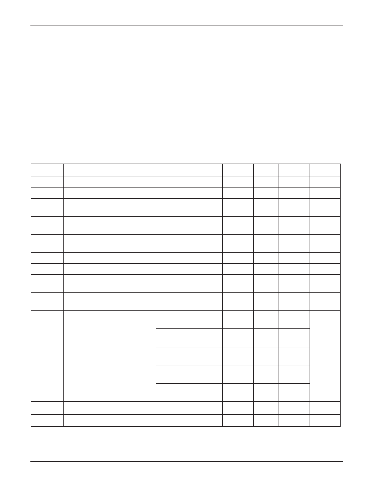
D.C. OPERATING CHARACTERISTICS
VCC = +3.0V to +5.5V and over the recommended temperature conditions unless otherwise specified.
lobmySretemaraPsnoitidnoCtseTniMpyTxaMstinU
I
IL
I
OL
I
1CC
I
2CC
I
BS
)1(
V
LI
)1(
V
HI
V
LO
V
HO
V
HT
V
DILAVR
)2(
V
TR
Notes:
1. VIL min and VIH max are reference values only and are not tested.
2. This parameter is tested initially and after a design or process change that affects the parameter. Not 100% tested.
,ADS( TESER )
)TESER(
tnerruCegakaeLtupnIV
tnerruCegakaeLtuptuOV
)etirW(tnerruCylppuSrewoP
)daeR(tnerruCylppuSrewoP
tnerruCybdnatS
NI
NI
f
LCS
V
CC
f
LCS
V
CC
V
NI
egatloVwoLtupnI5.0-ccVx3.0V
egatloVhgiHtupnIccVx7.05.0+ccVV
egatloVwoLtuptuO
egatloVhgiHtuptuO
dlohserhTteseR
VdilaVtuptuOteseR
CC
egatloV00.1V
I
LO
V
CC
I
HO
V
CC
V(
CC
V(
CC
V(
CC
V(
CC
V(
CC
siseretsyHdlohserhTteseR51Vm
ccVotDNG=2-01Aµ
ccVotDNG=01-01Aµ
zHk004=
V5.5=
zHk004=
V5.5=
,V5.5=ccV
ccVroDNG=
Am3=
V7.2=
Am4.0-=
V7.2=
54-x201TAC
)V5=
24-x201TAC
)V5=
03-x201TAC
)V3.3=
82-x201TAC
)V3.3=
52-x201TAC
)V3=
-ccV
57.0
05.457.4
52.405.4
00.351.3
58.200.3
55.207.2
3Am
1Am
04Aµ
4.0V
V
V
Doc. No. 3008, Rev. M
4
Page 5
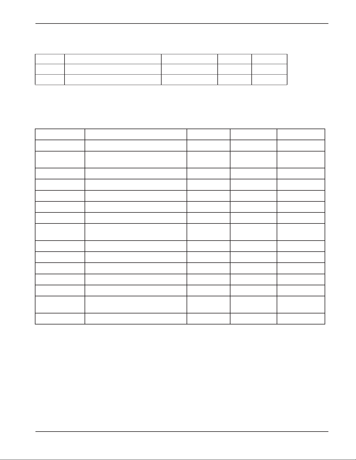
CAPACITANCE
TA = 25°C, f = 1.0 MHz, VCC = 5V
Symbol Test Test Conditions Max Units
(1)
C
C
OUT
(1)
IN
Output Capacitance V
= 0V 8 pF
OUT
Input Capacitance VIN = 0V 6 pF
AC CHARACTERISTICS
V
= 3.0V to 5.5V and over the recommended temperature conditions, unless otherwise specified.
CC
2
elcyCetirW&daeRyromeM
lobmySretemaraPniMxaMstinU
CAT1024, CAT1025
f
LCS
t
PS
t
WOL
t
HGIH
)1(
t
R
)1(
t
F
t
ATS;DH
t
ATS;US
t
TAD;DH
t
TAD;US
t
OTS;US
t
AA
t
HD
)1(
t
FUB
)3(
t
CW
ycneuqerFkcolC004zHk
ekipSretliFtupnI
)LCS,ADS(noisserppuS
001sn
doirePwoLkcolC3.1sµ
doirePhgiHkcolC6.0sµ
emiTesiRLCSdnaADS003sn
emiTllaFLCSdnaADS003sn
emiTdloHnoitidnoCtratS6.0sµ
emiTputeSnoitidnoCtratS
)tratSdetaepeRarof(
6.0sµ
emiTdloHtupnIataD0sn
emiTputeStupnIataD001sn
emiTputeSnoitidnoCpotS6.0sµ
dilaVtuOataDotwoLLCS009sn
emiTdloHtuOataD05sn
aerofeBeerFebtsumsuBehtemiT
tratSnaCnoissimsnarTweN
3.1sµ
)egaProetyB(emiTelcyCetirW5sm
Notes:
1. This parameter is characterized initially and after a design or process change that affects the parameter. Not 100% tested.
2. Test Conditions according to “AC Test Conditions” table.
3. The write cycle time is the time from a valid stop condition of a write sequence to the end of the internal program/erase cycle. During the write
cycle, the bus interface circuits are disabled, SDA is allowed to remain high and the device does not respond to its slave address.
5
Doc No. 3008, Rev. M
Page 6
CAT1024, CAT1025
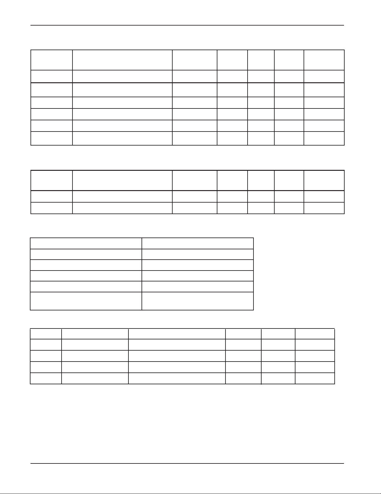
RESET CIRCUIT AC CHARACTERISTICS
lobmySretemaraP
t
TSRUP
t
DPR
t
HCTILG
V
HT
V
CC
hctilGRMytinummIhctilGteseRlaunaM1etoN001sn
t
WRM
t
DRM
GNIMITPU-REWOP
lobmySretemaraP
t
RUP
t
WUP
AC TEST CONDITIONS
tseT
snoitidnoC
niMpyTxaMstinU
tuoemiTteseR2etoN031002072sm
yaleDtuptuOTESERot3etoN5sµ
htdiWesluPtcejeRhctilG5,4etoN03sn
htdiWesluPRM1etoN5 sµ
yaleDtuptuOTESERottupnIRM1etoN1sµ
6,5
tseT
snoitidnoC
niMpyTxaMstinU
noitarepOdaeRotpU-rewoP 072sm
noitarepOetirWotpU-rewoP 072sm
retemaraPsnoitidnoCtseT
segatloVesluPtupnIV2.0
CC
V8.0ot
CC
semiTllaFdnaesiRtupnIsn01
segatloVecnerefeRtupnIV3.0
segatloVecnerefeRtuptuOV5.0
daoLtuptuO
C
L
V7.0,
CC
CC
CC
I:ecruoStnerruC
LO
;Am3=
Fp001=
RELIABILITY CHARACTERISTICS
Symbol Parameter Reference Test Method Min Max Units
(5)
N
END
(5)
T
DR
(5)
V
ZAP
(5)(7)
I
LTH
Notes:
1. Test Conditions according to “AC Test Conditions” table.
2. Power-up, Input Reference Voltage VCC = VTH, Reset Output Reference Voltage and Load according to “AC Test Conditions” Table
3. Power-Down, Input Reference Voltage VCC = VTH, Reset Output Reference Voltage and Load according to “AC Test Conditions” Table
4. VCC Glitch Reference Voltage = V
5. This parameter is characterized initially and after a design or process change that affects the parameter. Not 100% tested.
6. t
and t
PUR
7. Latch-up protection is provided for stresses up to 100mA on input and output pins from -1V to VCC + 1V.
Endurance MIL-STD-883, Test Method 1033 1,000,000 Cycles/Byte
Data Retention MIL-STD-883, Test Method 1008 100 Years
ESD Susceptibility MIL-STD-883, Test Method 3015 2000 Volts
Latch-Up JEDEC Standard 17 100 mA
; Based on characterization data
THmin
are the delays required from the time VCC is stable until the specified memory operation can be initiated.
PUW
Doc. No. 3008, Rev. M
6
Page 7

DEVICE OPERATION
Reset Controller Description
CAT1024, CAT1025
The CAT1024/25 precision RESET controllers ensure
correct system operation during brownout and power
up/down conditions. They are configured with open
drain RESET outputs.
During power-up, the RESET outputs remain active
until VCC reaches the VTH threshold and will continue
driving the outputs for approximately 200ms (t
after reaching VTH. After the t
timeout interval, the
PURST
PURST
device will cease to drive the reset outputs. At this point
the reset outputs will be pulled up or down by their
respective pull up/down resistors.
During power-down, the RESET outputs will be active
when V
valid so long as VCC is >1.0V (V
falls below VTH. The RESET output will be
CC
). The device is
RVALID
designed to ignore the fast negative going VCC transient
pulses (glitches).
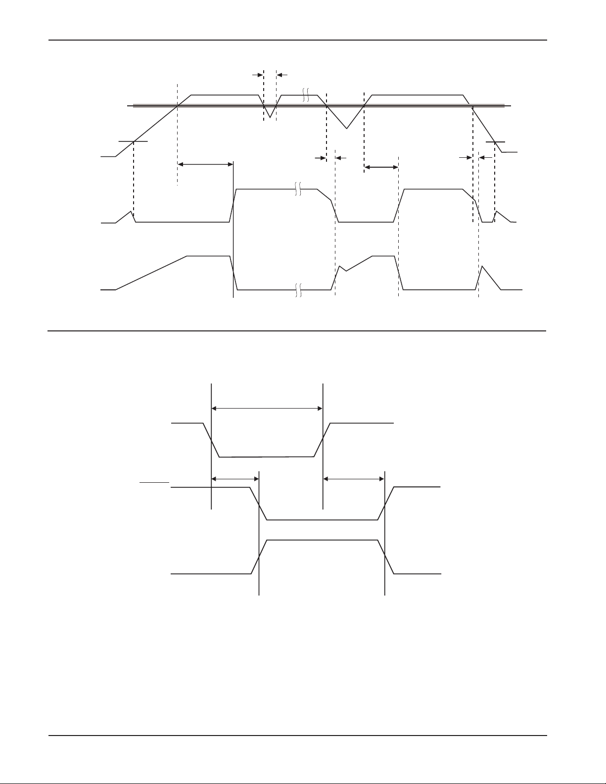
Reset output timing is shown in Figure 1.
Manual Reset Operation
The RESET pin can operate as reset output and manual
reset input. The input is edge triggered; that is, the
RESET input will initiate a reset timeout after detecting
a high to low transition.
including write operations. If the Reset output(s) are
active, in progress communications to the EEPROM are
aborted and no new communications are allowed. In this
condition an internal write cycle to the memory can not be
started, but an in progress internal non-volatile memory
write cycle can not be aborted. An internal write cycle
initiated before the Reset condition can be successfully
)
finished if there is enough time (5ms) before VCC reaches
the minimum value of 2V.
In addition, the CA T1025 includes a Write Protection Input
which when tied to VCC will disable any write operations
to the device.
When RESET I/O is driven to the active state, the 200
msec timer will begin to time the reset interval. If external
reset is shorter than 200 ms, Reset outputs will remain
active at least 200 ms.
CAT1024/25 also have a separate manual reset input.
Driving the MR input low by connecting a pushbutton
(normally open) from MR pin to GND will generate a
reset condition. The input has a internal pull up resistor.
Reset remains asserted while MR is low and for the
Reset Timeout period after MR input has gone high.
Glitches shorter than 100 ns on MR input will not
generate a reset pulse. No external debouncing circuits
are required. Manual reset operation using MR input is
shown in Figure 2.
Hardware Data Protection
The CAT1024/25 family has been designed to solve
many of the data corruption issues that have long been
associated with serial EEPROMs. Data corruption occurs
when incorrect data is stored in a memory location which
is assumed to hold correct data.
Whenever the device is in a Reset condition, the
embedded EEPROM is disabled for all operations,
7
Doc No. 3008, Rev. M
Page 8
CAT1024, CAT1025
Figure 1. RESET Output Timing
V
TH
V
RVALID
V
CC
RESET
RESET
t
PURST
t
GLITCH
t
RPD
t
PURST
t
RPD
Figure 2.
MRMR
MR Operation and Timing
MRMR
MR
RESET
RESET
t
MRD
t
MRW
t
PURST
Doc. No. 3008, Rev. M
8
Page 9
EMBEDDED EEPROM OPERATION
The CAT1024 and CAT1025 feature a 2kbit embedded
serial EEPROM that supports the I2C Bus data
transmission protocol. This Inter-Integrated Circuit Bus
protocol defines any device that sends data to the bus to
be a transmitter and any device receiving data to be a
receiver. The transfer is controlled by the Master device
which generates the serial clock and all START and
STOP conditions for bus access. Both the Master device
and Slave device can operate as either transmitter or
receiver, but the Master device controls which mode is
activated.
I2C Bus Protocol
The features of the I2C bus protocol are defined as
follows:
(1) Data transfer may be initiated only when the bus is
not busy.
(2) During a data transfer, the data line must remain
stable whenever the clock line is high. Any changes in
the data line while the clock line is high will be interpreted
as a START or STOP condition.
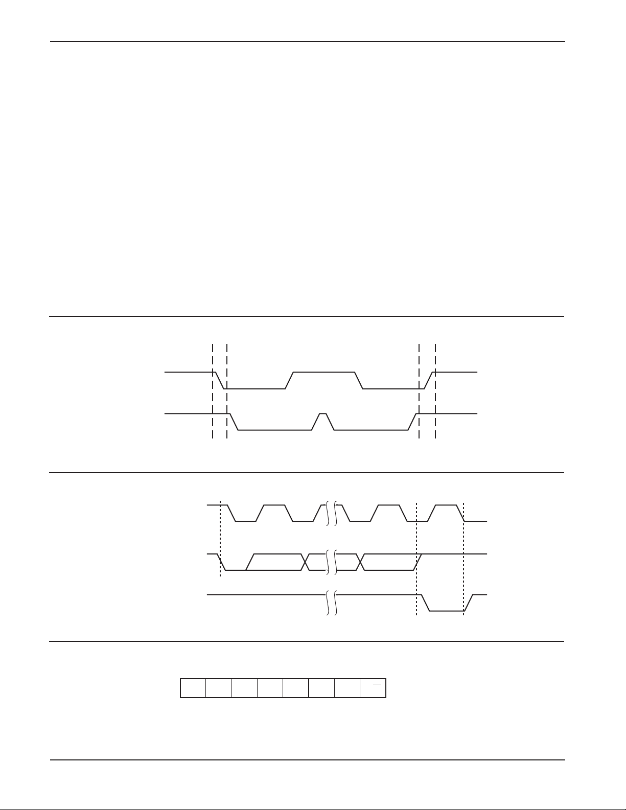
START Condition
The START Condition precedes all commands to the
device, and is defined as a HIGH to LOW transition of
CAT1024, CAT1025
SDA when SCL is HIGH. The CAT1024/25 monitors the
SDA and SCL lines and will not respond until this
condition is met.
STOP Condition
A LOW to HIGH transition of SDA when SCL is HIGH
determines the STOP condition. All operations must end
with a STOP condition.
DEVICE ADDRESSING
The Master begins a transmission by sending a START
condition. The Master sends the address of the particular
slave device it is requesting. The four most significant
bits of the 8-bit slave address are programmable in metal
and the default is 1010.
The last bit of the slave address specifies whether a
Read or Write operation is to be performed. When this bit
is set to 1, a Read operation is selected, and when set
to 0, a Write operation is selected.
After the Master sends a START condition and the slave
address byte, the CAT1024/25 monitors the bus and
responds with an acknowledge (on the SDA line) when
its address matches the transmitted slave address. The
CAT1024/25 then performs a Read or Write operation
depending on the R/W bit.
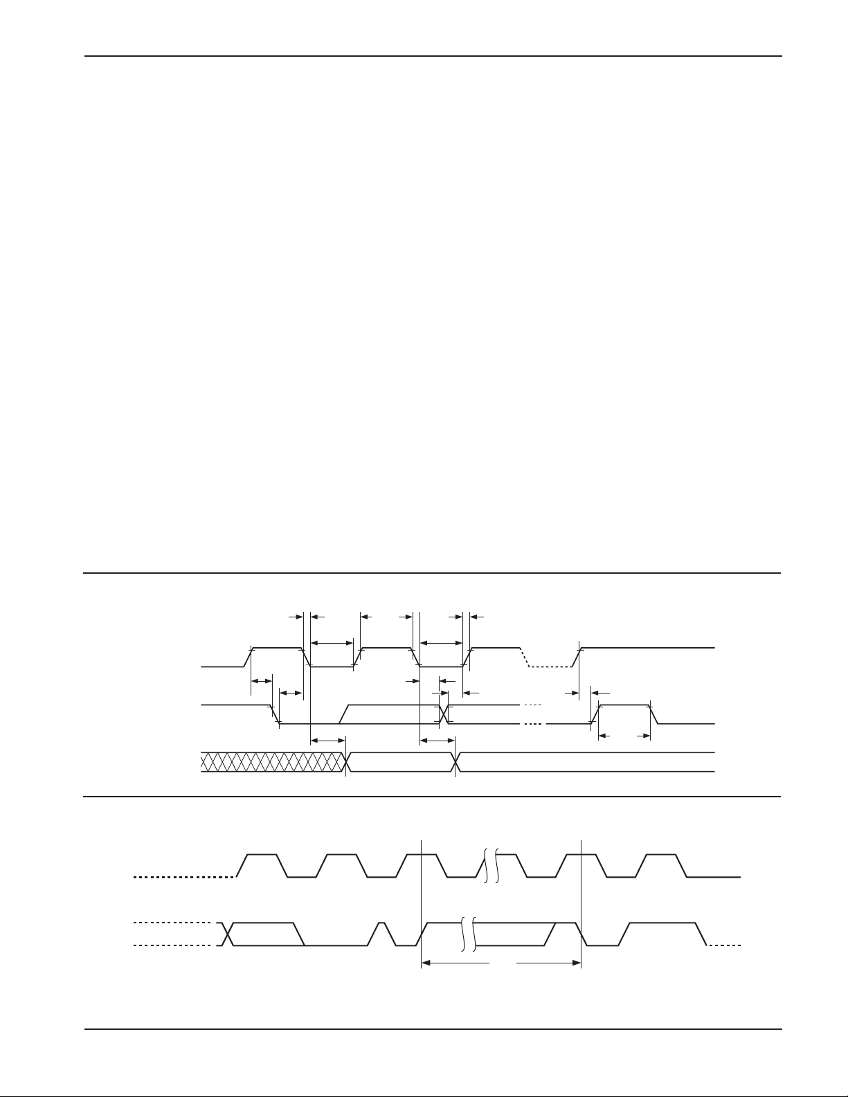
Figure 3. Bus Timing
SCL
t
SU:STA
SDA IN
SDA OUT
Figure 4. Write Cycle Timing
SCL
SDA
BYTE n
t
F
t
LOW
t
HD:STA
ACK8TH BIT
t
AA
t
HIGH
t
HD:DAT
t
LOW
t
DH
STOP
CONDITION
t
R
t
SU:DAT
t
WR
t
SU:STO
t
BUF
START
CONDITION
ADDRESS
9
Doc No. 3008, Rev. M
Page 10
CAT1024, CAT1025
ACKNOWLEDGE
After a successful data transfer, each receiving device
is required to generate an acknowledge. The
acknowledging device pulls down the SDA line during
the ninth clock cycle, signaling that it received the 8 bits
of data.
The CAT1024/25 responds with an acknowledge after
receiving a START condition and its slave address. If the
device has been selected along with a write operation,
it responds with an acknowledge after receiving each 8bit byte.
When the CAT1024/25 begins a READ mode it transmits
8 bits of data, releases the SDA line and monitors the
line for an acknowledge. Once it receives this
acknowledge, the CAT1024/25 will continue to transmit
data. If no acknowledge is sent by the Master, the device
terminates data transmission and waits for a STOP
condition.
Figure 5. Start/Stop Timing
WRITE OPERATIONS
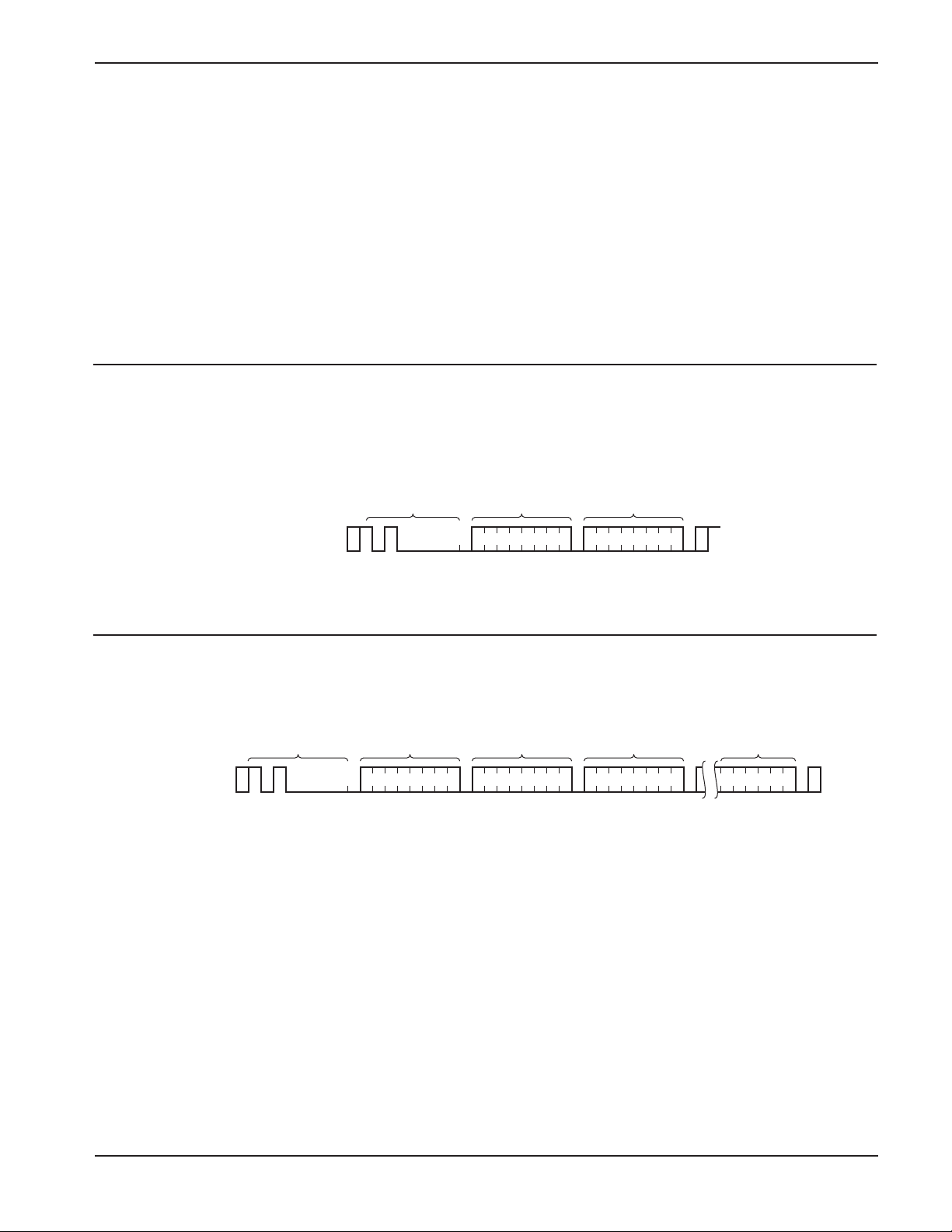
Byte Write
In the Byte Write mode, the Master device sends the
START condition and the slave address information (with
the R/W bit set to zero) to the Slave device. After the Slave
generates an acknowledge, the Master sends a 8-bit
address that is to be written into the address pointers of
the device. After receiving another acknowledge from the
Slave, the Master device transmits the data to be written
into the addressed memory location. The CAT1024/25
acknowledges once more and the Master generates the
STOP condition. At this time, the device begins an
internal programming cycle to non-volatile memory. While
the cycle is in progress, the device will not respond to any
request from the Master device.
SDA
SCL
Figure 6. Acknowledge Timing
SCL FROM
MASTER
DATA OUTPUT
FROM TRANSMITTER
DATA OUTPUT
FROM RECEIVER
Figure 7. Slave Address Bits
START BIT
START
STOP BIT
1
89
ACKNOWLEDGE
Default Configuration
Doc. No. 3008, Rev. M
CAT
1 010000R/W
10
Page 11
Page Write
CAT1024, CAT1025
The CAT1024/25 writes up to 16 bytes of data in a single
write cycle, using the Page Write operation. The page
write operation is initiated in the same manner as the byte
write operation, however instead of terminating after the
initial byte is transmitted, the Master is allowed to send up
to 15 additional bytes. After each byte has been
transmitted, the CAT1024/25 will respond with an
acknowledge and internally increment the lower order
address bits by one. The high order bits remain
unchanged.
Figure 8. Byte Write Timing
S
T
A
BUS ACTIVITY:
MASTER
SDA LINE
R
T
S
SLAVE
ADDRESS
If the Master transmits more than 16 bytes before sending
the STOP condition, the address counter ‘wraps around,’
and previously transmitted data will be overwritten.
When all 16 bytes are received, and the STOP condition
has been sent by the Master, the internal programming
cycle begins. At this point, all received data is written to
the CAT1024/25 in a single write cycle.
S
T
O
P
P
A
C
K
A
C
K
BYTE
ADDRESS
DATA
A
C
K
Figure 9. Page Write Timing
S
T
BUS ACTIVITY :
MASTER
SDA LINE
A
R
T
S
SLAVE
ADDRESS
ADDRESS (n)
A
C
K
BYTE
S
T
DATA n
A
C
K
A
C
K
DATA n+1
A
C
K
DATA n+15
O
P
P
A
C
K
11
Doc No. 3008, Rev. M
Page 12
CAT1024, CAT1025
Acknowledge Polling
Disabling of the inputs can be used to take advantage of
the typical write cycle time. Once the stop condition is
issued to indicate the end of the host’s write opration, the
CAT1024/25 initiates the internal write cycle. ACK polling
can be initiated immediately. This involves issuing the
start condition followed by the slave address for a write
operation. If the device is still busy with the write operation,
no ACK will be returned. If a write operation has
completed, an ACK will be returned and the host can
then proceed with the next read or write operation.
WRITE PROTECTION
The Write Protection feature (CAT1025 only) allows the
user to protect against inadvertent memory array
programming. If the WP pin is tied to V
Figure 10. Immediate Address Read Timing
, the entire
CC
memory array is protected and becomes read only. The
CAT1025 will accept both slave and byte addresses,
but the memory location accessed is protected from
programming by the device’s failure to send an
acknowledge after the first byte of data is received.
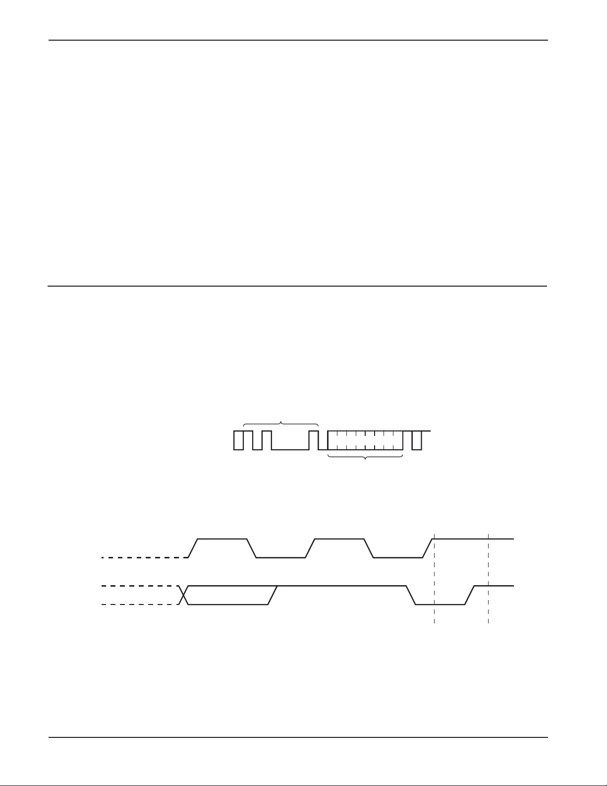
Read Operations
The READ operation for the CAT1024/25 is initiated in
the same manner as the write operation with one
exception, that R/W bit is set to one. Three different
READ operations are possible: Immediate/Current
Address READ, Selective/Random READ and
Sequential READ.
S
T
BUS ACTIVITY:
MASTER
SDA LINE
SCL
SDA 8TH BIT
A
R
T
S
89
SLAVE
ADDRESS
S
T
O
P
P
A
C
K
DATA
N
O
A
C
K
STOPNO ACKDATA OUT
Doc. No. 3008, Rev. M
12
Page 13
CAT1024, CAT1025
Immediate/Current Address Read
The CAT1024 and CAT1025 address counter contains
the address of the last byte accessed, incremented by
one. In other words, if the last READ or WRITE access
was to address N, the READ immediately following
would access data from address N+1. For N=E=255, the
counter will wrap around to zero and continue to clock
out valid data. After the CAT1024 and CAT1025 receives
its slave address information (with the R/W bit set to
one), it issues an acknowledge, then transmits the 8-bit
byte requested. The master device does not send an
acknowledge, but will generate a STOP condition.
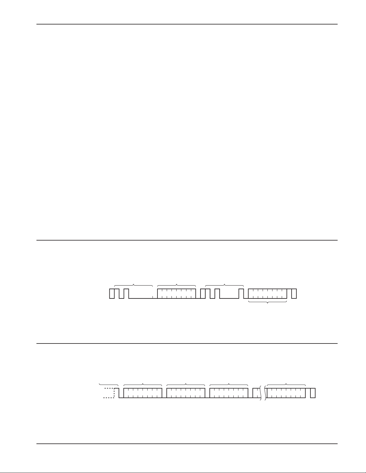
Selective/Random Read
Selective/Random READ operations allow the Master
device to select at random any memory location for a
READ operation. The Master device first performs a
‘dummy’ write operation by sending the START condition,
slave address and byte addresses of the location it
wishes to read. After the CAT1024 and CAT1025
acknowledges, the Master device sends the START
condition and the slave address again, this time with the
R/W bit set to one. The CAT1024 and CAT1025 then
responds with its acknowledge and sends the 8-bit byte
requested. The master device does not send an
acknowledge but will generate a STOP condition.
Sequential Read
The Sequential READ operation can be initiated by
either the Immediate Address READ or Selective READ
operations. After the CAT1024 and CAT1025 sends the
inital 8-bit byte requested, the Master will responds with
an acknowledge which tells the device it requires more
data. The CAT1024 and CAT1025 will continue to output
an 8-bit byte for each acknowledge, thus sending the
STOP condition.
The data being transmitted from the CAT1024 and
CAT1025 is sent sequentially with the data from address
N followed by data from address N+1. The READ
operation address counter increments all of the CAT1024
and CAT1025 address bits so that the entire memory
array can be read during one operation.
Figure 11. Selective Read Timing
S
T
BUS ACTIVITY:
MASTER
SDA LINE
A
R
T
S
SLAVE
ADDRESS
Figure 12. Sequential Read Timing
BUS ACTIVITY:
MASTER
SDA LINE
SLAVE
ADDRESS
A
C
K
BYTE
ADDRESS (n)
A
C
K
A
C
K
DATA n+1
A
C
K
S
T
A
R
T
S
A
C
K
SLAVE
ADDRESS
DATA n+2
S
T
O
P
P
A
DATA n
C
K
A
C
K
N
O
A
C
K
S
T
DATA n+xDATA n
O
P
P
N
O
A
C
K
13
Doc No. 3008, Rev. M
Page 14
CAT1024, CAT1025
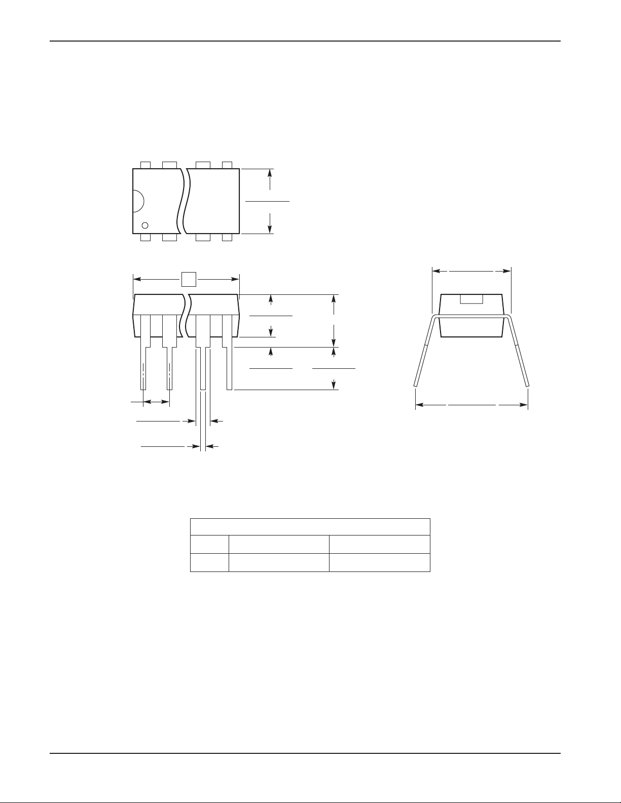
PACKAGE OUTLINES
8-LEAD 300 MIL WIDE PLASTIC DIP (P, L)
0.245 (6.17)
0.295 (7.49)
D
0.120 (3.05)
0.150 (3.81)
0.300 (7.62)
0.325 (8.26)
0.180 (4.57) MAX
0.100 (2.54)
BSC
0.045 (1.14)
0.060 (1.52)
0.014 (0.36)
0.022 (0.56)
0.015 (0.38)
—
0.110 (2.79)
0.150 (3.81)
Dimension D
Pkg Min Max
8L 0.355 (9.02) 0.400 (10.16)
0.310 (7.87)
0.380 (9.65)
Notes:
1. Complies with JEDEC Publication 95 MS001 dimensions; however, some of the dimensions may be more stringent.
2. All linear dimensions are in inches and parenthetically in millimeters.
Doc. No. 3008, Rev. M
14
Page 15
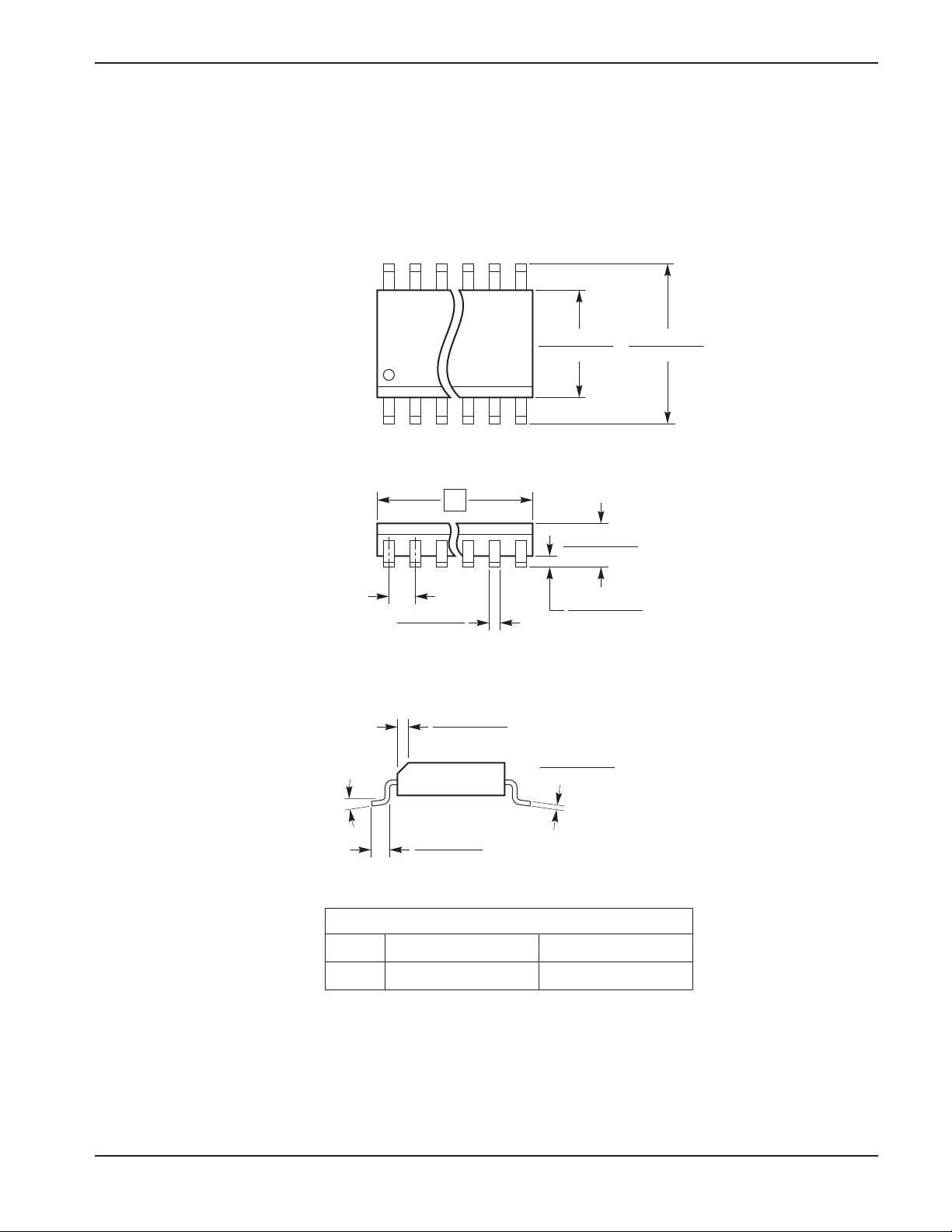
8-LEAD 150 MIL WIDE SOIC (J, W)
CAT1024, CAT1025
0.050 (1.27) BSC
D
0.013 (0.33)
0.020 (0.51)
0.0099 (0.25)
0.0196 (0.50)
0.1497 (3.80)
0.1574 (4.00)
X 45°
0.0075 (0.19)
0.0098 (0.25)
0.2284 (5.80)
0.2440 (6.20)
0.0532 (1.35)
0.0688 (1.75)
0.0040 (0.10)
0.0098 (0.25)
0°–8°
0.016 (0.40)
0.050 (1.27)
Dimension D
Pkg Min Max
8L 0.1890(4.80) 0.1968(5.00)
Notes:
1. Complies with JEDEC publication 95 MS-012 dimensions; however, some dimensions may be more stringent.
2. All linear dimensions are in inches and parenthetically in millimeters.
3. Lead coplanarity is 0.004" (0.102mm) maximum.
15
Doc No. 3008, Rev. M
Page 16
CAT1024, CAT1025
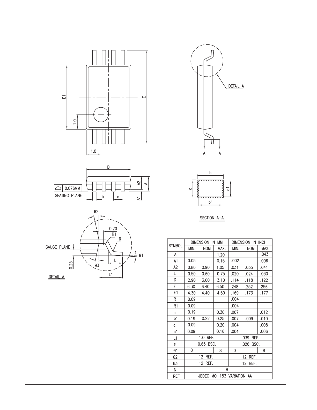
8-LEAD TSSOP (U, Y)
Doc. No. 3008, Rev. M
16
Page 17
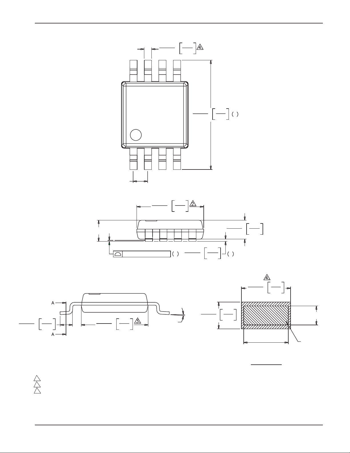
8 LEAD MSOP (R, Z)
0.0150
0.0110
CAT1024, CAT1025
0.38
0.28
0.0256 [0.65] BSC
0.0433 [1.10] MAX.
0.1220
0.1142
0.039 [0.10] MAX. S
3.10
2.90
0.1970
0.1890
0.0059
0.0020
0.15
0.05
5.00
4.80
S
0.0374
0.0295
S
0.95
0.75
0.0150
0.0110
WITH PLATING
0.23
0.13
0.0276
0.0157
0.70
0.40
0.1220
0.1142
3.10
2.90
0˚ - 6˚
0.0091
0.0051
WITH PLATING
0.0118 [0.30] REF.
Notes:
(1) All dimensions are in mm Angles in degrees.
2 Does not include Mold Flash, Protrusion or Gate Burrs. Mold Flash, Protrusions or Gate Burrs shall not exceed 0.15 mm. per side.
3 Does not include Interlead Flash orProtrusion. Interlead Flash or Protrusion shall not exceed 0.25 mm per side.
4 Does not include Dambar Protrusion, allowable Dambar Protrusion shall be 0.08 mm.
(5) This part is compliant with JEDEC Specification MO-187 Variations AA.
(6) Lead span/stand off height/coplanarity are considered as special characteristics. (S)
(7) Controlling dimensions in inches. [mm]
SECTION A - A
17
0.38
0.28
0.0050 [0.127]
BASE METAL
Doc No. 3008, Rev. M
Page 18
CAT1024, CAT1025
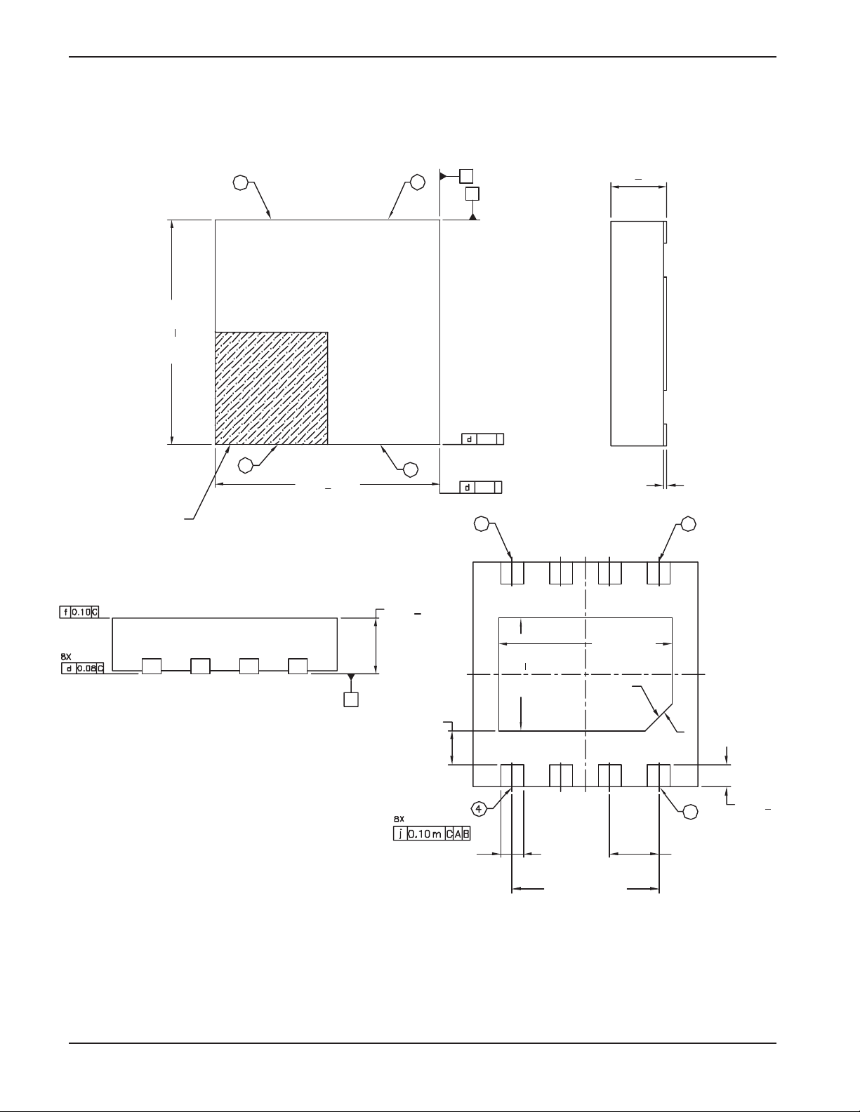
TDFN 3X3 PACKAGE (RD4, ZD4)
PIN 1 INDEX AREA
(S)
3.00 + 0.10
85
A
B
2X
0.15
C
1
3.00 + 0.10
4
2X
0.15
C
(S)
58
0.75 + 0.05
0.0 - 0.05
0.75 + 0.05
C
1.50 + 0.10
0.25 min.
0.30 + 0.07 (8x)
NOTE:
1. ALL DIMENSION ARE IN mm. ANGLES IN DEGREES.
2. COPLANARITY SHALL NOT EXCEED 0.08 mm.
3. WARPAGE SHALL NOT EXCEED 0.10 mm.
4. PACKAGE LENGTH / PACKAGE WIDTH ARE CONSIDERED AS SPECIAL CHARACTERISTIC(S)
5. REFER JEDEC MO-229 / WEEC
2.30 + 0.10
C0.35
1.95 REF. (2x)
PIN 1 ID
1
0.30 + 0.10 (8x)
0.65 TYP. (6x)
Doc. No. 3008, Rev. M
18
Page 19
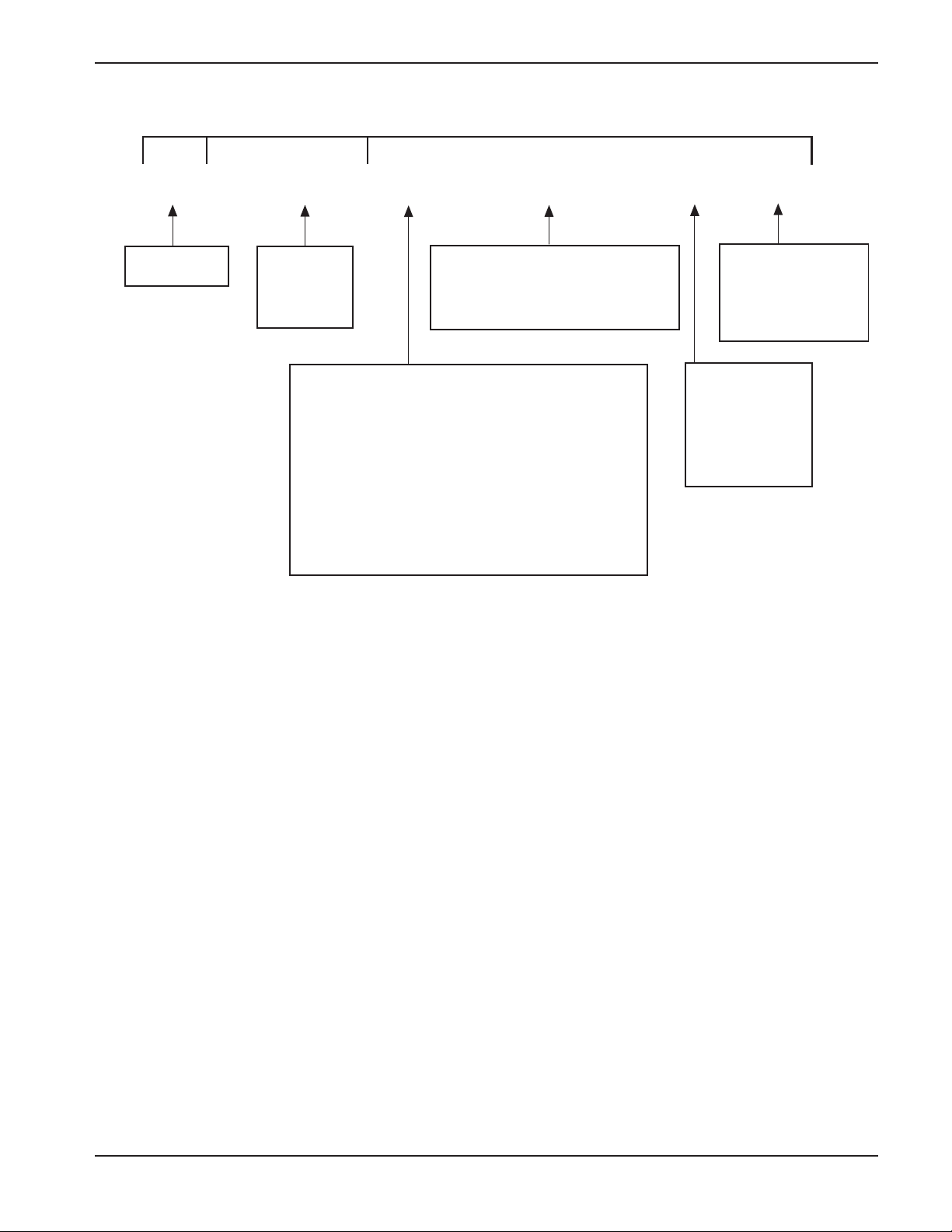
Ordering Information
Prefix Device # Suffix
CAT1024, CAT1025
CAT
Optional
Company ID
1024
Product
Number
1024: 2K
1025: 2K
J
I
Temperature Range
I = Industrial (-40˚C to 85˚C)
E = Extended Automotive
(-40˚C to +125˚C)
-30
TE13
Tape & Reel
SOIC: 2000/Reel
TSSOP: 2000/Reel
MSOP: 2500/Reel
TDFN: 2000/Reel
Package
P: PDIP
J: SOIC (JEDEC)
R: MSOP
U: TSSOP
RD4: 8-pad TDFN (3x3mm)
Reset Threshold
Voltage
45: 4.5-4.75V
42: 4.25-4.5V
30: 3.0-3.15V
28: 2.85-3.0V
25: 2.55-2.7V
L: PDIP (Lead free, Halogen free)
W: SOIC (JEDEC, Lead free, Halogen free)
Z: MSOP Lead free, Halogen free)
Y: TSSOP (Lead free, Halogen free)
ZD4: 3x3mm TDFN (Lead free, Halogen free)
Note:
(1) The device used in the above example is a CAT1024JI-30TE13 (Supervisory circuit with I2C serial 2k CMOS EEPROM, SOIC, Industrial
Temperature, 3.0-3.15V Reset Threshold Voltage, Tape and Reel).
19
Doc No. 3008, Rev. M
Page 20
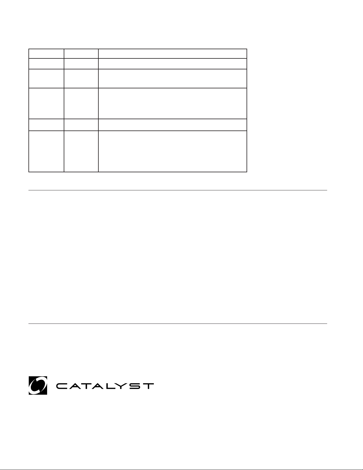
REVISION HISTORY
Date Rev. Reason
11/7/03 I Eliminated Automotive temperature range
4/12/2004 J Eliminated data sheet designation
Updated Reel Ordering Information
11/1/2004 K Changed SOIC package designators
Eliminated 8-pad TDFN (3x4.9mm) package
Added package outlines
11/04/04 L Update Pin Configuration
11/11/04 M Update Features
Update Description
Updae DC Operating Characteristic
Update AC Characteristics
Copyrights, Trademarks and Patents
Trademarks and registered trademarks of Catalyst Semiconductor include each of the following:
DPP ™ AE2 ™
I2C is a trademark of Philips Corporation
Catalyst Semiconductor has been issued U.S. and foreign patents and has patent applications pending that protect its products. For a complete list of patents
issued to Catalyst Semiconductor contact the Company’s corporate office at 408.542.1000.
CATALYST SEMICONDUCTOR MAKES NO WARRANTY, REPRESENTATION OR GUARANTEE, EXPRESS OR IMPLIED, REGARDING THE SUITABILITY OF ITS
PRODUCTS FOR ANY PARTICULAR PURPOSE, NOR THAT THE USE OF ITS PRODUCTS WILL NOT INFRINGE ITS INTELLECTUAL PROPERTY RIGHTS OR THE
RIGHTS OF THIRD PARTIES WITH RESPECT TO ANY PARTICULAR USE OR APPLICATION and SPECIFICALLY DISCLAIMS ANY and ALL LIABILITY ARISING
OUT OF ANY SUCH USE OR APPLICATION, INCLUDING BUT NOT LIMITED TO, CONSEQUENTIAL OR INCIDENTAL DAMAGES.
Catalyst Semiconductor products are not designed, intended, or authorized for use as components in systems intended for surgical implant into the body, or
other applications intended to support or sustain life, or for any other application in which the failure of the Catalyst Semiconductor product could create a
situation where personal injury or death may occur.
Catalyst Semiconductor reserves the right to make changes to or discontinue any product or service described herein without notice. Products with data sheets
labeled "Advance Information" or "Preliminary" and other products described herein may not be in production or offered for sale.
Catalyst Semiconductor advises customers to obtain the current version of the relevant product information before placing orders. Circuit diagrams illustrate
typical semiconductor applications and may not be complete.
Catalyst Semiconductor, Inc.
Corporate Headquarters
1250 Borregas Avenue
Sunnyvale, CA 94089
Phone: 408.542.1000
Fax: 408.542.1200
www.catalyst-semiconductor.com
Publication #: 3008
Revison: M
Issue date: 11/11/04
 Loading...