

Page 1

CAT809, CAT810
N
E
G
F
O
R
L
A
H
E
E
3-Pin Microprocessor Power Supply Supervisors
FEATURES
■ Precision monitoring of
+5.0 V (+/- 5%, +/- 10%, +/- 20%),
+3.3 V (+/- 5%, +/ 10%),
+3.0 V (+/- 10%) and
+2.5 V (+/- 5%) power supplies
■ Offered in two output configurations:
- CAT809: Active LOW reset
- CAT810: Active HIGH reset
■ Direct replacements for the MAX809 and
■ Reset valid down to V
■ 6 µA power supply current
■ Power supply transient immunity
■ Compact 3-pin SOT23 and SC70 packages
■ Industrial temperature range: -40˚C to +85˚C
APPLICATIONS
■ Computers
■ Servers
■ Laptops
■ Cable modems
■ Wireless communications
■ Embedded control systems
■ White goods
■ Power meters
■ Intelligent instruments
■ PDAs and handheld equipment
L
E
A
D
MAX810 in applications operating over the
industrial temperature range
= 1.0 V
CC
E
E
TM
R
F
DESCRIPTION
The CAT809 and CAT810 are µP supervisory circuits
that monitor power supplies in digital systems. The
CAT809 and CAT810 are direct replacements for the
MAX809 and MAX810 in applications operating over the
industrial temperature range.
These devices generate a reset signal, which is asserted
while the power supply voltage is below a preset threshold
level and for at least 140 ms after the power supply level
has risen above that level. The underlying floating gate
technology, AE
makes it possible to offer any custom reset threshold
value. Seven industry standard threshold levels are
2(TM)
used by Catalyst Semiconductor,
THRESHOLD SUFFIX SELECTOR
Nominal Threshold Threshold Suffix
Voltage Designation
4.63V L
4.38V M
4.00V J
3.08V T
2.93V S
2.63V R
2.32V Z
offered to support +5.0 V, +3.3 V, +3.0 V and +2.5 V
systems.
The CAT809 features a RESET push-pull output (active
LOW) and the CAT810 features a RESET push-pull
output (active HIGH).
Fast transients on the power supply are ignored and the
output is guaranteed to be in the correct state at V
levels as low as 1.0 V.
The CAT809/810 are fully specified over the industrial
temperature range (-40˚C to 85˚C) and are available in
compact 3-pin SOT23 and SC70 packages.
PIN CONFIGURATION
1
GND
RESET
(RESET)
CAT809
(CAT810)
2
3-Lead SOT23
3-Lead SC70
3
V
CC
cc
© 2004 by Catalyst Semiconductor, Inc., Patent Pending
Characteristics subject to change without notice
1
Doc. No. 3004, Rev. S
Page 2

CAT809, CAT810
ORDERING INFORMATION
rebmuNtraPgniredrOytiraloPTESERegakcaPleeRrepstraP
T-RUE_908TAClluP-hsuP TESER 32TOS,nip-3k3
01T-RUE_908TAClluP-hsuP TESER 32TOS,nip-3k01
T-IBT_908TAClluP-hsuP TESER neerG32TOS,nip-3k3
01T-IBT_908TAClluP-hsuP TESER neerG32TOS,nip-3k01
T-RXE_908TAClluP-hsuP TESER 07CS,nip-3k3
01T-RXE_908TAClluP-hsuP TESER 07CS,nip-3k01
T-IDS_908TAClluP-hsuP TESER neerG07CS,nip-3k3
01T-IDS_908TAClluP-hsuP TESER neerG07CS,nip-3k01
T-RUE_018TACTESERlluP-hsuP32TOS,nip-3k3
01T-RUE_018TACTESERlluP-hsuP32TOS,nip-3k01
T-IBT_018TAC
01T-IBT_018TAC
_018TACRXET-lluP-hsuPTESER
_018TACRXE01T-lluP-hsuPTESER
T-IDS_018TAC
01T-IDS_018TAC
Insert threshold suffix (L, M, J, T, S, R or Z) into the blank position. Example: CAT809LTBI-T for 4.63 V.
lluP-hsuPTESER
lluP-hsuPTESER
lluP-hsuPTESER
lluP-hsuPTESER
TOP MARKING
32TOSneerG32TOS07CSneerG07CS
L908TACMYAAMYBD_AF_AG
M908TACMYBAMYCD_BF_BG
J908TACMYWCMYAD_GF_GG
T908TACMYCAMYFD_EF_EG
S908TACMYDAMYED_DF_DG
R908TACMYFAMYDD_CF_CG
Z908TACMYFCMYGD_FF_FG
neerG32TOS,nip-3k3
neerG32TOS,nip-3k01
07CS,nip-3k3
07CS,nip-3k01
neerG07CS,nip-3k3
neerG07CS,nip-3k01
L018TACMYGAMYKC_HF_HG
M018TACMYHAMYLC_JF_JG
J018TACMYIAMYJC_PF_PG
T018TACMYJAMYPC_MF_MG
S018TACMYKAMYNC_LF_LG
R018TACMYLAMYMC_KF_KG
Z018TACMYGCMYRC_NF_NG
Where YM stands for Year and Month for the SOT23 package and the blank is replaced by the assembly location for the SC70 package.
Doc. No. 3004, Rev. S Patent Pending
2
Page 3

PIN DESCRIPTIONS
CAT809, CAT810
Pin Number
Name Description
CAT809 CAT810
1 1 GND Ground
2—RESET Active LOW reset. RESET is asserted if V
falls below the reset threshold
CC
and remains low for at least 140ms after VCC rises above the reset threshold.
— 2 RESET Active HIGH reset. RESET is asserted if VCC falls below the reset
threshold and remains high for at least 140ms after VCC rises above
the reset threshold.
33VCCPower supply voltage that is monitored.
Patent Pending Doc. No. 3004, Rev. S
3
Page 4

CAT809, CAT810
ABSOLUTE MAXIMUM RATINGS*
Any pin with respect to ground .......... -0.3 V to +6.0 V
Input Current, VCC............................................. 20 mA
Output Current, RESET, RESET ...................... 20 mA
Rate of Rise, V
.............................................................
CC
Continuous Power Dissipation
Derate 2.2mW/˚C above 70˚C (SC70)......... 175 mW
Derate 4mW/˚C above 70˚C (SOT23) ......... 320 mW
100 V/µs
Operating Temperature Range........... -40°C to +85°C
Storage Temperature Range............ -65°C to +105°C
Lead Soldering Temperature (10 sec).............. 300°C
*COMMENT
Stresses above those listed under “Absolute Maximum Ratings” may
cause permanent damage to the device. These are stress ratings only,
and functional operation of the device at these or any other conditions
outside of those listed in the operational sections of this specification is not
implied. Exposure to any absolute maximum rating for extended periods
may affect device performance and reliability.
ELECTRICAL CHARACTERISTICS
= Full range, TA = -40°C to +85°C unless otherwise noted. Typical values at TA = +25˚C and V
V
CC
L/M/J versions, V
Parameter Symbol Conditions Min Typ Max Units
VCC Range TA = 0˚C to +70˚C 1.0 5.5
Supply Current I
Reset
Threshold
Voltage
= 3.3 V for the T/S versions, V
CC
TA = -40˚C to +85˚C 1.2 5.5
CC
V
TH
TA = -40˚C to +85˚C
L Threshold
M Threshold
J Threshold
T Threshold
S Threshold
R Threshold
Z Threshold
= 3 V for the R version and V
CC
VCC < 5.5 V, J/L/M 8 20
VCC < 3.6 V, R/S/T/Z 6 15
TA = +25˚C 4.56 4.63 4.70
TA = -40˚C to +85˚C 4.50 4.75
TA = +25˚C 4.31 4.38 4.45
TA = -40˚C to +85˚C 4.25 4.50
TA = +25˚C 3.93 4.00 4.06
TA = -40˚C to +85˚C 3.89 4.10
TA = +25˚C 3.04 3.08 3.11
TA = -40˚C to +85˚C 3.00 3.15
TA = +25˚C 2.89 2.93 2.96
TA = -40˚C to +85˚C 2.85 3.00
TA = +25˚C 2.59 2.63 2.66
TA = -40˚C to +85˚C 2.55 2.70
TA = +25˚C 2.28 2.32 2.35
TA = -40˚C to +85˚C 2.25 2.38
= 2.5 V for the Z version.
CC
= 5 V for the
CC
µA
V
V
Doc. No. 3004, Rev. S Patent Pending
4
Page 5

CAT809, CAT810
ELECTRICAL CHARACTERISTICS
= Full range, TA = -40˚C to +85˚C unless otherwise noted. Typical values at TA = +25˚C and V
V
CC
L/M/J versions, V
= 3.3 V for T/S versions, V
CC
Parameter Symbol Conditions Min Typ
(continued)
= 3 V for R version and V
CC
= 2.5 V for Z version.
CC
CC
(1)
Max Units
= 5 V for
Reset Threshold Tempco 30 ppm/˚C
VCC to Reset Delay (Note 2) VCC = VTH to (VTH - 100 mV) 20 µs
Reset Active Timeout Period TA = -40˚C to +85˚C 140 240 400 ms
RESET Output Voltage Low
(Push-pull, active LOW,
CAT809)
RESET Output Voltage High
(Push-pull, active LOW,
CAT809)
RESET Output Voltage Low
(Push-pull, active HIGH,
CAT810)
VCC = VTH min, I
CAT809R/S/T/Z
V
OL
VCC = VTH min, I
CAT809J/L/M
VCC > 1.0 V, I
VCC = VTH max, I
V
OH
VCC = VTH max, I
CAT809R/S/T/Z
CAT809J/L/M
VCC > VTH max, I
CAT810R/S/T/Z
V
OL
VCC > VTH max, I
= 1.2 mA
SINK
= 3.2 mA
SINK
= 50 µA 0.3
SINK
= 500 µA
SOURCE
SOURCE
= 800 µA
0.8 V
CC
VCC - 1.5
= 1.2 mA
SINK
= 3.2 mA
SINK
0.3
0.4
0.3
0.4
CAT810J/L/M
V
V
V
RESET Output Voltage High
(Push-pull active HIGH,
V
OH
1.8 V < VCC ≤ VTH min, I
= 150 µA 0.8 V
SOURCE
CAT810)
Note 1: Production testing done at TA = +25˚C; limits over temperature guaranteed by design only.
Note 2: RESET output for the CAT809; RESET output for the CAT810
CC
V
Patent Pending Doc. No. 3004, Rev. S
5
Page 6
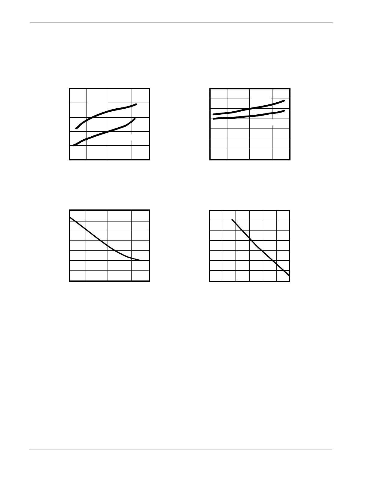
CAT809, CAT810
TYPICAL OPERATING CHARACTERISTICS
= Full range, TA = -40˚C to +85˚C unless otherwise noted. Typical values at TA = +25˚C and V
V
CC
L/M/J versions, V
=3.3 V for T/S versions, VCC = 3 V for R version and VCC = 2.5 V for Z version.
CC
CC
= 5 V for
POWER-UP RESET TIMEOUT
VS. TEMPERATURE
260
240
220
200
180
POWER-UP RESET TIMEOUT (mS)
160
-50 0 50 100 150
VCC=5V
VCC=2.5V
TEMPERATURE (˚C)
POWER-DOWN RESET DELAY VS. TEMPERATURE
14
12
10
8
6
4
2
0
POWER-DOWN RESET DELAY (µS)
-50 0 50 100 150
(CAT8xxR/S/T/Z)
TEMPERATURE (˚C)
SUPPLY CURRENT VS. TEMPERATURE
(NO LOAD, CAT8xxR/S/T/Z)
12
10
8
6
4
SUPPLY CURRENT (µA)
2
0
-50 0 50 100 150
VCC=5.5V
TEMPERATURE (˚C)
NORMALIZED RESET THRESHOLD
VS. TEMPERATURE
1.0002
1
0.9998
0.9996
0.9994
0.9992
0.999
NORMALIZED THRESHOLD
0.9988
0 20 40 60 80 100 120
TEMPERATURE (˚C)
VCC=3.6V
Doc. No. 3004, Rev. S Patent Pending
6
Page 7
CAT809, CAT810
DETAILED DESCRIPTIONS
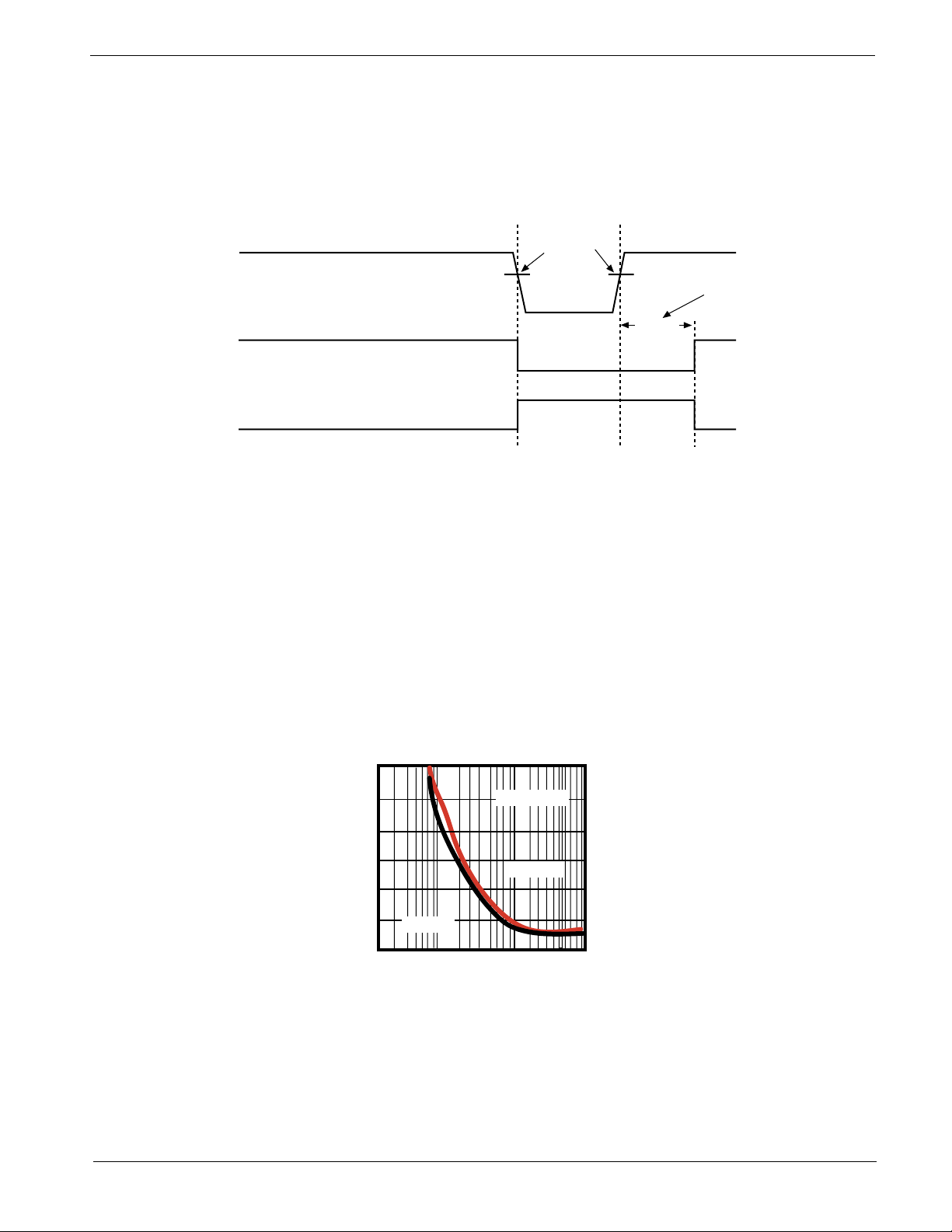
RESET TIMING
The reset signal is asserted LOW for the CAT809 and HIGH for the CAT810 when the power supply voltage falls below
the threshold trip voltage and remains asserted for at least 140ms after the power supply voltage has risen above the
threshold.
Threshold
Power
Supply
Voltage
RESET
5V
0V
5V
0V
Voltage
Reset Timeout Period
140ms
minimum
CAT809
RESET
5V
0V
CAT810
FIGURE 1. RESET TIMING DIAGRAM
VCC TRANSIENT RESPONSE
The CAT809/810 protect µPs against brownout failure. Short duration transients of 4µsec or less and 100 mV
amplitude typically do not cause a false RESET.
Figure 2 shows the maximum pulse duration of negative-going VCC transients that do not cause a reset condition. As
the amplitude of the transient goes further below the threshold (increasing VTH - VCC), the maximum pulse duration
decreases. In this test, the VCC starts from an initial voltage of 0.5V above the threshold and drops below it by the
amplitude of the overdrive voltage (VTH - VCC).
30
T
= 25°C
25
20
AMB
15
10
5
TRANSIENT DURATION [µs)
CAT809M
0
1 10 100 1000
RESET OVERDRIVE VTH - VCC [mV]
CAT809Z
FIGURE 2. Maximum Transient Duration Without Causing a Reset Pulse vs. Reset Comparator Overdrive
Patent Pending Doc. No. 3004, Rev. S
7
Page 8
CAT809, CAT810
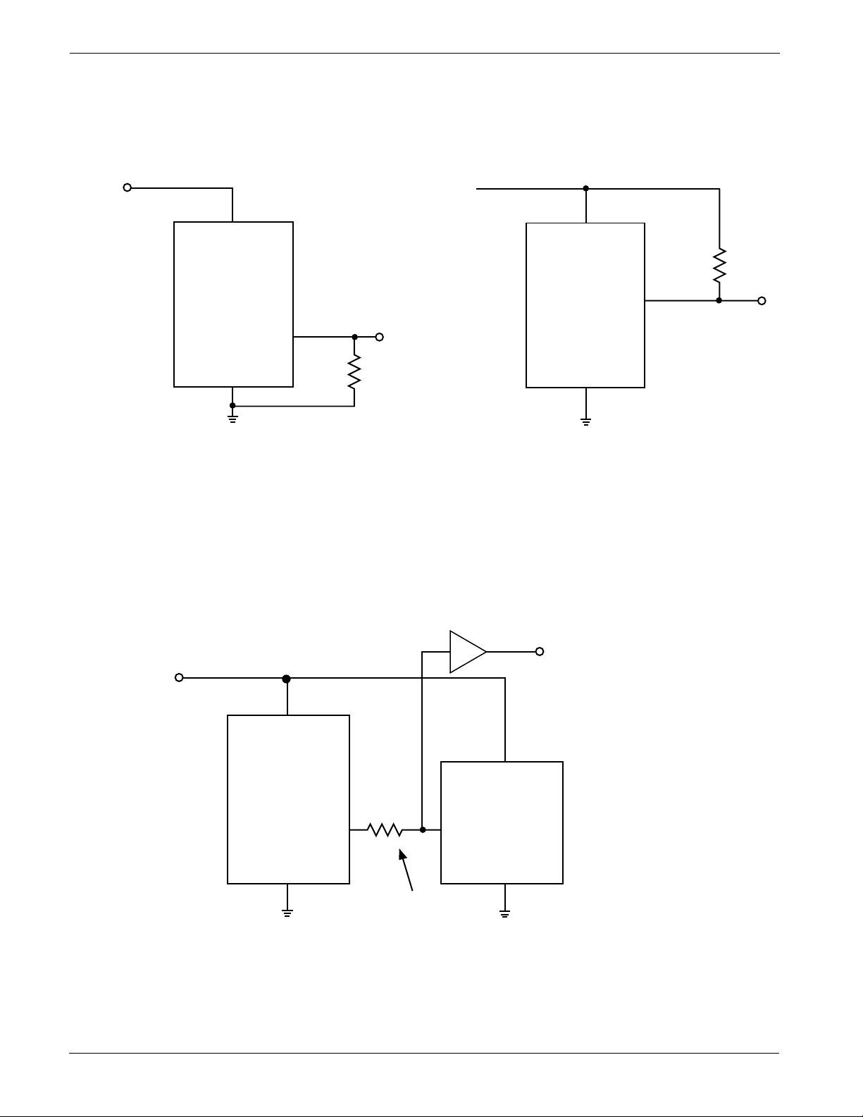
VALID RESET WITH VCC UNDER 1.0 V
To ensure that the CAT809 RESET pin is in a known state when V
between RESET pin and GND is recommended; the value is not critical. For the CAT810, a pull-up resistor from
RESET pin to VCC is needed.
is under 1.0 V, a 100 kΩ pull-down resistor
CC
Power
Supply
FIGURE 3.
V
CC
CAT809
RESET
GND
RESETRESET
RESET Valid with VCC Under 1.0 V
RESETRESET
100kΩ
Power
Supply
V
CC
CAT810
RESET
GND
FIGURE 4. RESET Valid with VCC Under 1.1 V
100kΩ
BI-DIRECTIONAL RESET PIN INTERFACING
The CAT809/810 can interface with µP/µC bi-directional reset pins by connecting a 4.7 kΩ resistor in series with the
CAT809/810 reset output and the µP/µC bi-directional reset pin.
Power
Supply
BUF
V
CC
CAT809
4.7kΩ
RESET
RESET
INPUT
GND
Bi-directional I/O Pin
FIGURE 5. Bi-directional Reset Pin Interfacing
µP
GND
Buffered
RESET
(For example: 68HC11)
Doc. No. 3004, Rev. S Patent Pending
8
Page 9
CAT809, CAT810
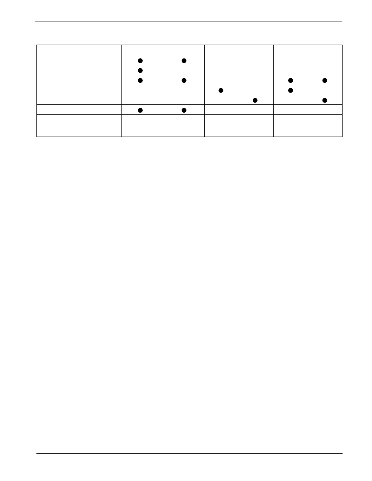
OTHER SUPERVISORY PRODUCTS
Function CAT1161/3 CAT1162 CAT809 CAT810 CAT811 CAT812
With 16k Bit Serial EEPROM Memory
Watchdog Timer
Manual Reset Input
Active Low Reset
Active High Reset
Dual Polarity Reset Outputs
Package 8-pin 8-pin 3-pin 3-pin 4-pin 4-pin
DIP and SOIC DIP and SOIC SOT23 and SOT23 and SOT143 SOT143
SC70 SC70
Patent Pending Doc. No. 3004, Rev. S
9
Page 10
CAT809, CAT810
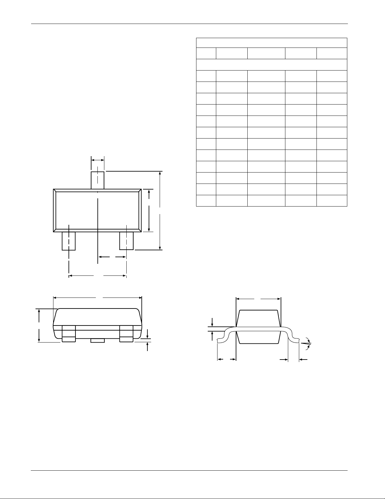
PACKAGE INFORMATION
Plastic SOT-23 (3-Pin)
Inches Millimeters
Min Max Min Max
Plastic SOT-23 (3-Pin)
A 0.0350 0.0441 0.89 1.12
A1 0.0005 0.0039 0.013 0.10
B 0.0146 0.0197 0.37 0.50
c 0.0033 0.0071 0.085 0.18
D 0.1102 0.1197 2.80 3.04
E 0.0472 0.0551 1.20 1.40
e 0.0350 0.0406 0.89 1.03
B
e1 0.0701 0.0807 1.78 2.05
H 0.0827 0.1039 2.10 2.64
∝ 0° 8° 0° 8°
L 0.0083 0.0161 0.275 0.41
E
H
L1 0.0160 0.0270 0.275 0.685
NOTE:
1. THIS PART IS COMPLIANT WITH JEDEC
SPECIFICATION TO-236AB
2. DIE IS FACE UP FOR MOLD AND TRIM/FORM
3. DIMENSIONS ARE EXCLUSIVE OF MOLD
e
FLASH AND METAL BURR
e1
D
c
A
A1
L1
E
∝
L
Doc. No. 3004, Rev. S Patent Pending
10
Page 11
CAT809, CAT810
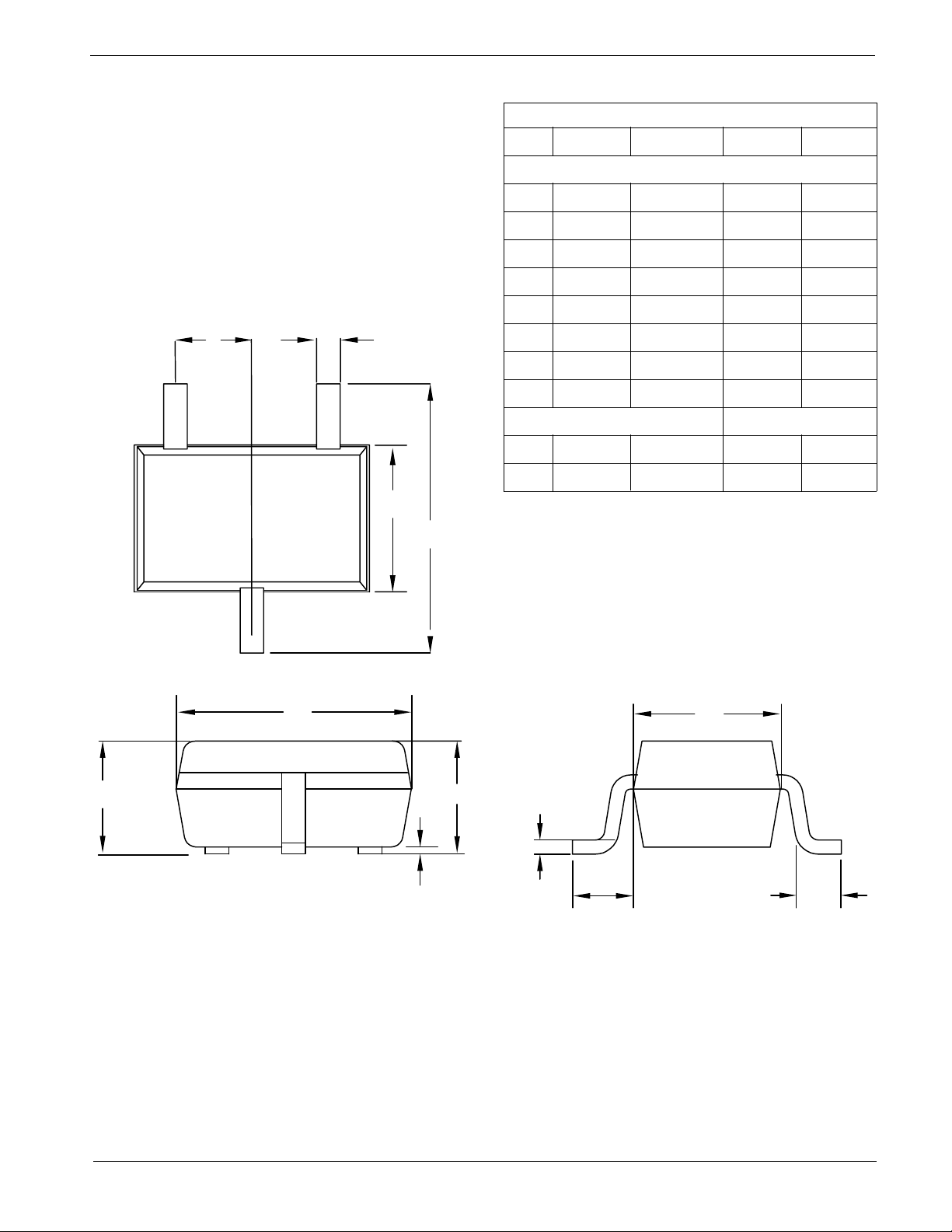
PACKAGE INFORMATION
SC-70 Package (3-Lead)
eb
21
3
Inches Millimeters
Min Max Min Max
Plastic SC-70 (3-Pin)
A 0.0315 0.0433 0.80 1.10
A1 0.0000 0.0039 0.00 0.10
A2 0.0315 0.0394 0.80 1.00
b 0.0059 0.00118 0.15 0.30
c 0.0035 0.0071 0.09 0.18
D 0.0709 0.0866 1.80 2.20
E 0.0453 0.0531 1.15 1.35
E1 0.0709 0.0945 1.80 2.40
e 0.00255 BSC 0.65BSC
L 0.0102 0.0181 0.26 0.46
L1 0.0108 0.0226 0.275 0.575
E
E1
NOTE:
1. THIS PART IS COMPLIANT WITH EIAJ
SPECIFICATION SC-70
2. DIE IS FACE UP FOR MOLD. DIE IS FACING
DOWN FOR TRIM/FORM
3. DIMENSIONS ARE EXCLUSIVE OF MOLD
FLASH AND METAL BURR
D
A2 A
A1
E
c
L1 L
Patent Pending Doc. No. 3004, Rev. S
11
Page 12

CAT809, CAT810
REVISION HISTORY
Date Rev. Reason
10/29/2003 N Updated VCC Transient Response text and Figure 2
10/30/2003 O Updated Power Up Reset Timeout vs. Temperature curve
3/10/2004 P Corrected temperature range
Updated Description
Updated Ordering Information
Updated Absolute Maximum Ratings
Updated Electrical Characteristics
03/23/2004 Q Updated Description
Updated Ordering Information
Updated Absolute Maximum Ratings
Updated Electrical Characteristics
Updated Typical Operating Characteristics
Updated Package Information
3/25/2004 R Changed Preliminary designation to Final
Updated Max Reset Active Timout Period in Electrical Characteristics
Updated package drawings
5/10/2004 S Updated top marking table
Doc. No. 3004, Rev. S Patent Pending
12
Page 13

Copyrights, Trademarks and Patents
Trademarks and registered trademarks of Catalyst Semiconductor include each of the following:
DPP ™ AE2 ™
Catalyst Semiconductor has been issued U.S. and foreign patents and has patent applications pending that protect its products. For a complete list of patents
issued to Catalyst Semiconductor contact the Company’s corporate office at 408.542.1000.
CATALYST SEMICONDUCTOR MAKES NO WARRANTY, REPRESENTATION OR GUARANTEE, EXPRESS OR IMPLIED, REGARDING THE SUITABILITY OF ITS
PRODUCTS FOR ANY PARTICULAR PURPOSE, NOR THAT THE USE OF ITS PRODUCTS WILL NOT INFRINGE ITS INTELLECTUAL PROPERTY RIGHTS OR THE
RIGHTS OF THIRD PARTIES WITH RESPECT TO ANY PARTICULAR USE OR APPLICATION AND SPECIFICALLY DISCLAIMS ANY AND ALL LIABILITY ARISING
OUT OF ANY SUCH USE OR APPLICATION, INCLUDING BUT NOT LIMITED TO, CONSEQUENTIAL OR INCIDENTAL DAMAGES.
Catalyst Semiconductor products are not designed, intended, or authorized for use as components in systems intended for surgical implant into the body, or
other applications intended to support or sustain life, or for any other application in which the failure of the Catalyst Semiconductor product could create a
situation where personal injury or death may occur.
Catalyst Semiconductor reserves the right to make changes to or discontinue any product or service described herein without notice. Products with data sheets
labeled "Advance Information" or "Preliminary" and other products described herein may not be in production or offered for sale.
Catalyst Semiconductor advises customers to obtain the current version of the relevant product information before placing orders. Circuit diagrams illustrate
typical semiconductor applications and may not be complete.
Catalyst Semiconductor, Inc.
Corporate Headquarters
1250 Borregas Avenue
Sunnyvale, CA 94089
Phone: 408.542.1000
Fax: 408.542.1200
www.catalyst-semiconductor.com
Publication #: 3004
Revison: S
Issue date: 5/10/04
Patent Pending
 Loading...