

Page 1
WK-1200
100 RHYTHMS
ENVELOPE
AMP ENVELOPE
PITCH ENVELOPE
000-048 DECAY
MAX
MIN
00 FLAT049-137 SUSTAIN 01-19 VIBRATO 20-49 OTHERS
TEMPO ACCOMP VOLUME
S
Y
O
R
T
N
I
N
O
R
M
A
L
/
F
I
L
L
-
I
N
REVERB
REVERB
SYNTH
HALL
STAGE
ROOM
SYNTH
MIXER
MIXER
N
C
H
R
O
/
E
N
D
I
N
G
N
I
-
L
L
I
F
/
R
A
V
MEMORY
STEP
MEMORY
STEP
CHORD/1 2 3 4 5 6
POWER
MODE
VOLUME
FULL RANGE
CHORD
FINGERED
CASIO CHORD
NORMAL
ELECTRONIC KEYBOARD
MUSICAL INFORMATION SYSTEM
MEMORY TRACK/DRUM PAD
200TONES
TRANSPOSE/
TUNE/MIDI
RHYTHM TONE
FREE SESSION
GM
FREE
SESSION
LAYER
LAYER
SPLIT
TOUCH
RESPONSE
SPLIT
S
O
R
R
U
C
TOUCH
RESPONSE
REST
ENTER
DEMO
TIE
3
WK-1200
Page 2

CONTENTS
Page
Specifications............................................................................................................................................ 1
Block Diagram........................................................................................................................................... 3
Circuit Description..................................................................................................................................... 4
Adjustment .............................................................................................................................................. 12
Major Waveforms .................................................................................................................................... 13
Printed Circuit Boards ............................................................................................................................. 14
Schematic Diagrams ............................................................................................................................... 15
Exploded View ........................................................................................................................................ 21
Parts List ................................................................................................................................................. 23
SPECIFICATIONS
GENERAL
Keyboard: 73 standard-size keys, 6 octaves (with touch response on/off)
Drum pads: 6
Tones: 200 (128 General MIDI, 32 synthesized, 8 drum, 32 user); with layer and
split
Rhythm instrument tones: 51
Polyphony: 24 notes maximum (12 for certain tones)
Digital effects: 3 reverb types (HALL, STAGE, ROOM)
Auto accompaniment
Rhythm patterns: 100
Tempo: Variable (216 steps, = 40 to 255)
Chords: 3 fingering methods (CASIO CHORD, FINGERED, FULL RANGE
CHORD)
Rhythm controller: START/STOP, INTRO, NORMAL /FILL-IN, VAR/FILL-IN, SYNCHRO/
ENDING
Accomp volume: 0 to 127 (128 steps)
Free session
Number of patterns 100 (auto-accompaniment in accordance with selected chord progres-
sion)
Memory function
Songs: 2
Recording tracks: 6 (2 through 6 are melody tracks)
Recording methods: Real-time, step
Memory capacity: Approximately 5,200 notes (total for two songs)
Edit function: Equipped
Demo tunes: 2
Synthesizer function
Parameters: PCM set, amp envelope set, attack rate, release rate, pitch envelope set,
pitch, level, touch sense, pan
Mixer function
Channels: 16
Parameters: Program change number, volume, expression, pan, coarse tuning, fine
tuning, on/off/solo
MIDI: 16 multi-timbre receive, GM Level 1 standard
Other functions
Pitch bend range: 12 semitones upwards and downwards
Transpose: 25 steps (–12 semitones to +12 semitones)
Tuning: Variable (A4 = approximately 440 Hz ± 50 cents)
— 1 —
Page 3

Terminals
MIDI terminals: IN, OUT
Assignable terminal: Standard jack (sustain, sostenuto, soft, rhythm start/stop)
Headphone/Output terminal: Stereo standard jack
Output Impedance: 200 Ω
Output Voltage: 4.9 V (RMS) MAX
Power supply terminal: 12 V DC
Power supply Dual power supply system
Batteries: Six D-size batteries
Battery life: Approximately 2 hours (UM-1/R20) 8 hours (AM-1/LR20)
AC adaptor: AD-12
Auto power off: Turns power off approximately six minutes after last key operation. En-
abled under battery power only, can be disabled manually.
Power consumption: 12 V --- 18 W
Speaker output: 5 W + 5 W
Dimensions (HWD): 116.2 × 42.1 × 14.7 cm (45-13/16 × 16-9/16 × 5-13/16 inches)
Weight: Approximately 9.1 kg (20.1 lbs) (without batteries)
ELECTRICAL
Current drain with 12 V DC:
No sound output 430 mA ± 20 %
Maximum volume 1570 mA ± 20 %
with 24 keys from C4 to C6 pressed in Bassoon tone
Volume: maximum, Touch response: maximum
Reverb: Hall
Phone output level (Vrms with 8 Ω load each channel):
with key A5 pressed in Bassoon tone L-ch 165 mV ± 20 %
Volume: maximum R-ch 150 mV ± 20 %
Reverb: Hall
Speaker output level (Vrms with 4 Ω load each channel):
with key A5 pressed in Bassoon tone L-ch 5500 mV ± 20 %
Volume: maximum R-ch 5200 mV ± 20 %
Reverb: Hall
Output level (Vrms with 47 kΩ load each channel):
with key A5 pressed in Bassoon tone L-ch 4260 mV ± 20%
R-ch 3950 mV ± 20%
Minimum operating voltage: 6.3 V
About General MIDI
General MIDI standardizes MIDI data for all sound source types, regardless of manufacturer. General MIDI
specifies such factors as tone numbering, drum sounds, and available MIDI channels for all sound sources.
This standard makes it possible for all MIDI equipment to reproduce the same nuances when playing
General MIDI data, regardless of the manufacturer of the sound source.
This keyboard supports General MIDI, so it can be used to play commercially available pre-recorded
General MIDI data and General MIDI data send to it from a personal computer.
— 2 —
Page 4
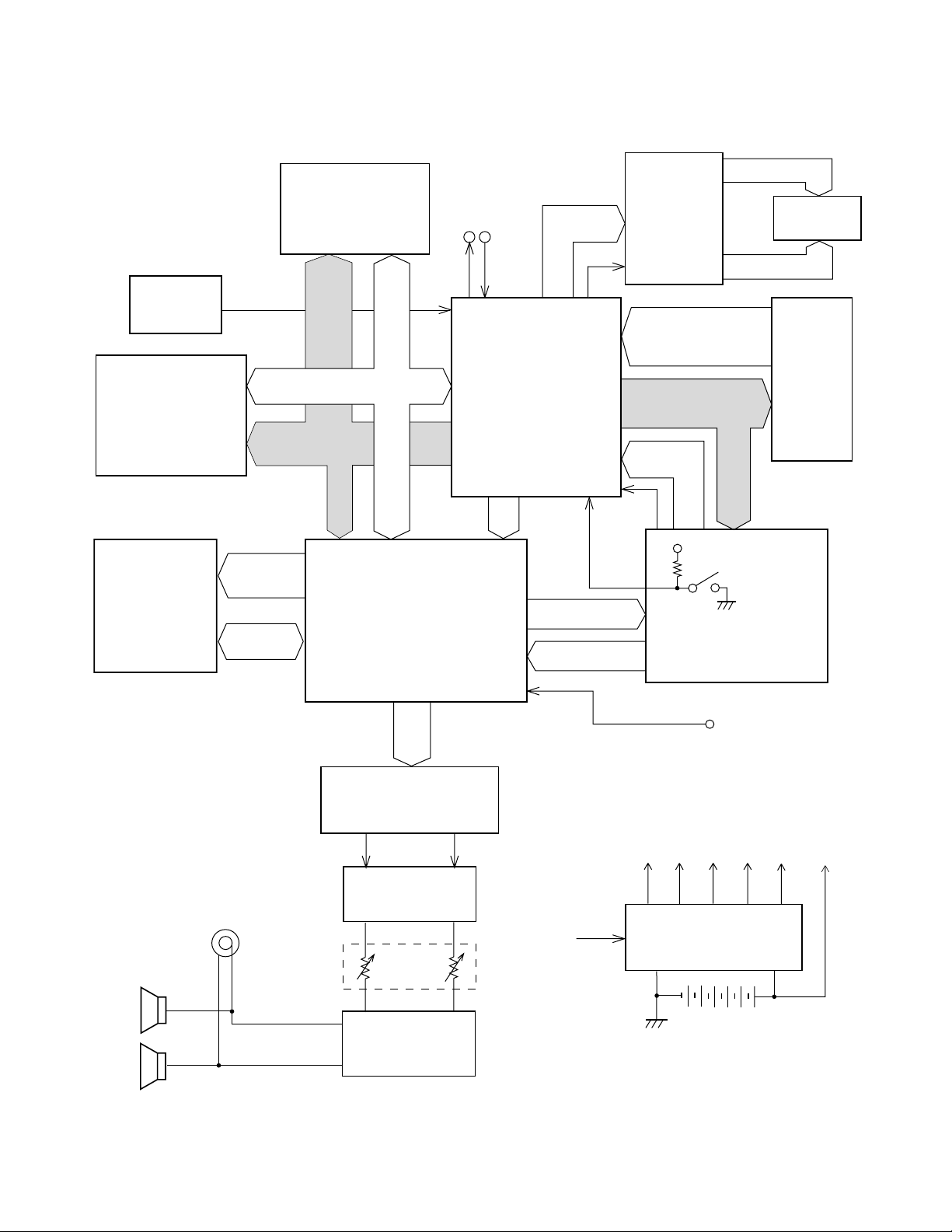
BLOCK DIAGRAM
Reset IC
IC2
RN5VD40AA
Sound Source ROM
(16M-bit)
LSI3
MX23C1610MC-
12CA64
Effect RAM
(256K-bit)
LSI5
TC55257DFL-
70L(EL)
RESET
MA0 ~ MA19
MA0, MA1
EA0 ~
EA14
EIO0 ~
EIO7
Working Storage
RAM (256K-bit)
LSI4
TC55257DFL-70L(EL)
MA0
~
MA14
MD0 ~ MD15
MD0
~
MD7
DSP
LSI2
HG51B277FB-1
MIDI
LRCK, SO
BCK, SINK
INOUT
GT-913F
CPU
LSI1
P10, P13
P14, P17
P23
NMI
PA0 ~ PA5
PB0 ~ PB3
LCD Driver
LSI501
SED1278F0A
FI0 ~ FI9
SI0 ~ SI9
KC0 ~ KC7
KI0 ~ KI2
PB0 ~ PB3
FI10
VDD
SEG1 ~ SEG40
LCD
COM1 ~ COM16
Keyboard
Power Switch
Buttons
Speakers
Output
LRCK
SO
BCK
D/A Converter
IC1
UPD6379GR
Filter
Q308 ~ Q311
Main
Volume
Power Amplifier
IC301
LA4620
PB4
APO
Assingnable Jack
CVDDLVDD
VCC
Q301 ~ Q304, 306, 307
AVDD
Power Supply Circuit
D307, 310
VC
VDD
— 3 —
Page 5

CIRCUIT DESCRIPTION
KEY MATRIX
0CK1CK2CK3CK4CK5CK6CK7CK
0IF)1(1C)1(1#C)1(1D)1(1#D)1(1E)1(1F)1(1#F)1(1G
0IS)2(1C)2(1#C)2(1D)2(1#D)2(1E)2(1F)2(1#F)2(1G
1IF)1(1#G)1(1A)1(1#A)1(1B)1(2C)1(2#C)1(2D)1(2#D
1IS)2(1#G)2(1A)2(1#A)2(1B)2(2C)2(2#C)2(2D)2(2#D
2IF)1(2E)1(2F)1(2#F)1(2G)1(2#G)1(2A)1(2#A)1(2B
2IS)2(2E)2(2F)2(2#F)2(2G)2(2#G)2(2A)2(2#A)2(2B
3IF)1(3C)1(3#C)1(3D)1(3#D)1(3E)1(3F)1(3#F)1(3G
3IS)2(3C)2(3#C)2(3D)2(3#D)2(3E)2(3F)2(3#F)2(3G
4IF)1(3#G)1(3A)1(3#A)1(3B)1(4C)1(4#C)1(4D)1(4#D
4IS)2(3#G)2(3A)2(3#A)2(3B)2(4C)2(4#C)2(4D)2(4#D
5IF)1(4E)1(4F)1(4#F)1(4G)1(4#G)1(4A)1(4#A)1(4B
5IS)2(4E)2(4F)2(4#F)2(4G)2(4#G)2(4A)2(4#A)2(4B
6IF)1(5C)1(5#C)1(5D)1(5#D)1(5E)1(5F)1(5#F)1(5G
6IS)2(5C)2(5#C)2(5D)2(5#D)2(5E)2(5F)2(5#F)2(5G
7IF)1(5#G)1(5A)1(5#A)1(5B)1(6C)1(6#C)1(6D)1(6#D
7IS)2(5#G)2(5A)2(5#A)2(5B)2(6C)2(6#C)2(6D)2(6#D
8IF)1(6E)1(6F)1(6#F)1(6G)1(6#G)1(6A)1(6#A)1(6B
8IS)2(6E)2(6F)2(6#F)2(6G)2(6#G)2(6A)2(6#A)2(6B
9IF)1(7C
9IS)2(7C
Key
Note: Each key has two contacts,
the first conatct (1) and second contact (2).
FI
Second contact (2)
First contact (1)
KC
SI
NOMENCLATURE OF KEYS
C#1 D#1 F#1 G#1 A#1
C#2 D#2 F#2 G#2 A#2 C#3 D#3 F#3 G#3 A#3 C#4 D#4 F#4 G#4 A#4 C#5 D#5 F#5 G#5 A#5 C#6 D#6 F#6 G#6 A#6
C2
D2 E2 F2 G2 A2 B2C1 D1 E1 F1 G1 A1 B1 C3 D3 E3 F3 G3 A3 B3
C4 D4 E4 F4 G4 A4 B4 C5 D5 E5 F5 G5 A5 B5 D6 E6 F6 G6 A6 B6C6 C7
— 4 —
Page 6

BUTTON MATRIX
KC0 KC1 KC2 KC3 KC4 KC5 KC6 KC7
DRUM DRUM PITCH
FI10 PAD 3 PAD 1 BEND
CHORD 3 CHORD 1 H
DRUM DRUM PITCH G
KI0 PAD 4 PAD 2 BEND
CHORD 4 CHORD 2 G
DRUM
KI1 PAD 5 STEP
CHORD 5
DRUM
KI2 PAD 6 MEMORY
CHORD 6
PA0 PA1 PA2 PA3
FULL RANGE
PB0
PB1 FINGERED
PB2
PB3 NORMAL
CHORD RESPONSE
NORMAL/ FREE ACCOMP
FILL-IN SESSION VOLUME
CASIO SYNCHRO/
CHORD ENDING
VARIATION/
FILL-IN
INTRO
TEMPO
TEMPOG TRANSPOSE/
H
ENTER
START/
STOP
H
G
TOUCH
LAYER SYNTH
SPILIT MIXER
E 7 2 0 DEMO
F 451
REVERB
9 6 + TONE
8 3 — RHYTHM
TUNE/MIDI
POWER SUPPLY CIRCUIT
The power supply circuit generates five voltages as shown in the following table. VDD and VC voltages
are always generated. The others are controlled by APO signal from the CPU.
Name Voltage For operation of
VDD +5 V CPU, Reset IC, DSP, Sound source ROM, Working storage RAM, Effect RAM
AVDD +5 V DAC, Filter
LVDD +5.6 V LCD driver
VCC,VC +9 V Power amplifier, Pilot lamp
CVDD +5 V Power jack, Pedal jack, MIDI jacks, Source voltage for LCD backlight
— 5 —
Page 7

LCD BACKLIGHT
Q501
23 32
NT-07
10 1
11
HMBV26BG1W63N/AZ
DE0405-979SL180J2K
2
2
C502
CFL1
9
8
7
5
(Bottom View)
T501
2
3
4
5
R501
1
C501
1
Q502
12
4.7K
LHL08TB101K
2SD965R 2SD965R
C104M
12
L501
C516
1
CP14
DG
C104FA
12
CVDD
When voltage CVDD is supplied, transistors Q501 and 502 start oscillation.
From the oscillation voltage, transformer T501 generates about 600 V which is necessary for lighting the
backlight.
RESET CIRCUIT
When batteries are set or an AC adapter is connected, the reset IC provides a low pulse to the CPU. The
CPU then initializes its internal circuit, and clears the working storage RAM.
When the power switch is pressed, the CPU receives a low pulse of POWER signal. The CPU sends APO
signal to the power supply circuit, also sends a reset signal to the DSP.
Battery set
VDD
Reset IC
IC2
RN5VD40AA
POWER
From power switch
RESET
NMI
CPU
LSI1
GT-913F
VDD
PLE
SCKO
Reset signal
APO
VDD
DSP
LSI2
HG51B277FB-1
To power supply circuit
— 6 —
Page 8
CPU (LSI1: GT-913F)
The 16-bit CPU contains a 1k-byte RAM, three 8-bit I/O ports, two timers, a key controller and serial interfaces.
The CPU detects key velocity by counting the time between first-key input signal FI and second-key SI from
the keyboard. The CPU reads sound data and velocity data from the sound source ROM in accordance with
the selected tone; the CPU can read rhythm data simultaneously when a rhythm pattern is selected. Then the
CPU provides 16-bit serial sound data to the DSP. The CPU also controls MIDI input/output and stores
sequencer data into the working storage RAM.
The following table shows the pin functions of LSI1.
.oNniPlanimreTtuO/nInoitcnuF
10DXTtuOtuptuolangisIDIM
20DXRnItupnilangisIDIM
30KCStuOtuptuolangis)ffOrewoPotuA(OPA
5,4
61KCStuOtuptuoeslupgnizinorhcnysZHM1
7CCVAnIecruos)V5+(DDVC
80NAnI
91NAnIrednebhctipmorftupnI
01DNGAnIecruos)V0(dnuorG
11KCBtuOtuptuokcolctiB
21OStuOtuptuoataddnuoslaireS
31KCRLtuOtuptuokcolcdroW
41DNGnIecruos)V0(dnuorG
61,511TLX,0TLXtuO/nItuptuo/tupnikcolczHM03
71CCVnIecruosV5+
91,811DOM,0DOMnIlanimretnoitcelesedoM
02BTSRnItupnilangisteseR
12IMNnItupnilangisNOrewoP
2201P/TNItuO/nIrevirdDCLehtrofsubataD
03~32
83~137CK~0CKtuOlangisnacsyekroflanimreT
05~93
1501IFnIlangistupninottubroflanimreT
2532P/01IStuOrevirdDCLehtroflangiselbanepihC
55~352IK~0IKnIlangistupninottubroflanimreT
65BNWMtuOPSDehtroflangiselbaneetirW
67~7591AM~0AMtuOsubsserddA
770BSCMtuOMORecruosdnuosehtroftuptuolangiselbanepihC
871BSCMtuOdesutoN
972BSCMtuOPSDehtroftuptuolangiselbanepihC
,31P/DXT
41P/DXR
3IF~0IF
3IS~0IS
9IF~4IF
9IS~4IS
tuO/nIrevirdDCLehtrofsubataD
nIlangistupniyekroflanimreT
nIlangistupniyekroflanimreT
.lanimretnoitcetedrotpadaCA
V0semocebdnaseirettabybderewopsidraobyekehtnehwV5+
.detcennocsirotpadaCAnehwnoitcnufOPAehtlecnacot
— 7 —
Page 9

.oNniPlanimreTtuO/nInoitcnuF
08CCVnIecruosV5+
18DNGnIecruos)V0(dnuorG
28BDRMtuOMORecruosdnuosehtroftuptuolangiselbanedaeR
89~3851DM~0DMtuO/nIsubataD
99ELPtuOPSDehtroftuptuolangisteseR
00171PtuO/nIrevirdDCLehtrofsubataD
DIGITAL SIGNAL PROCESSOR (LSI2: HG51B227FB-1)
The DSP receives 16-bit serial sound data output from the CPU and adds the selected effect to the sound data
using the effect RAM. Then the DSP provides the sound data to the DAC. The DSP also controls button input/
output.
The following table shows the pin functions of LSI2.
.oNniPlanimreTtuO/nI
08,3~13BP~0BPnIslanimrettupninottuB
44BPnItupnikcaJELBANGISSA
5OStuOCADehtroftuptuoataddnuoslaireS
6OKCWtuOCADehtroftuptuokcolcdroW
73DDVnIecruosV5+
8TSET—desutoN
9BSERnItupnilangisteseR
012SSVnIecruos)V0(dnuorG
21,11TUOX,NIXtuO/nItuptuo/tupnikcolczHM02
31IKCWnIUPCehtmorftupnikcolcdroW
41ISnIUPCehtmorftupniataddnuoslaireS
51IKCBnIUPCehtmorftupnikcolctiB
61CNISnItupnieslupgnizinorhcnyszHM1
712DDVnIecruosV5+
52~817OI~0OItuO/nIsubataD
62BECRtuOMARegarotsgnikrowehtroftuptuolangiselbanepihC
723SSVnIecruos)V0(dnuorG
821DAnIsubsserddA
92BEDnIMARegarotsgnikrowroflangiselbaneataD
03BEWnIlangiselbaneetirW
133DDVnIecruosV5+
232ECnI.evitcahgiH.tupnilangiselbanepihC
330DAnIsubsserddA
43B1ECnI.evitcawoL.tupnilangiselbanepihC
34,14~537OIE~0OIEtuO/nIMARtceffeehtrofsubataD
,84~64,44,24
16,95~15
54BECEtuOMARtceffeehtroftuptuolangiselbanepihC
41AE~0AEtuOMARtceffeehtrofsubsserddA
noitcnuF
— 8 —
Page 10

Pin No. Terminal In/Out Function
49 EOEB Out Read enable signal output for the effect RAM
50 VSS3 In Ground (0 V) source
60 BWEB Out Write enable signal output for the effect RAM
62, 66, 70, 74, 78 VSS2 In Ground source
63, 67, 71, 75, 79 VDD2 In +5 V source
64, 65, 68, 69,
72, 73
76, 77 PA6/7 Out Not used
PA0 ~ PA5 Out Button scan signal output
LCD DRIVER (LSI501 : SED1278F0A)
The LCD driver can drive a dot matrix LCD having 40 segment and 16 common lines. The LSI contains 240
graphic symbols in the built-in character generator ROM, and stores 80 characters in the built-in display data
RAM. In accordance with command from the CPU, the LSI is capable of displaying up to 16 characters
simultaneously. The following table shows the pin functions of LSI 501.
Pin No. Terminal In/Out Function
1 ~ 22,
63 ~ 80
23 VSS — GND (0 V) source
24, 25 OSC1, OSC2 In/Out
SEG1 ~ SEG40 Out Segment signal output
Terminals for the built-in clock pulse generator. The external
resistor connected determines the oscillation frequency.
LCD drive voltage input.
26 ~ 30 V1 ~ V5 In
31, 32 LP, XSCL — Not used
33 VDD In LVDD (+5 V) source
34, 35 FR, DO — Not used
36 RS In
37 R/W In Read/write terminal. High: read, Low: write
38 E In
39 ~ 42 DB0 ~ DB3 — Not used. Connected to GND (0 V)
43 ~ 46 DB4 ~ DB7 In/Out Data bus
47 ~ 62 COM1 ~ COM16 Out Common signal/output
Those voltages are used forgenerating the stepped pulse of
the LCD drive signals.
Data/command determination terminal.High: data, Low:
command
Chip enable signal.
High: enable, the writing is done at fall edge.
Low: disenable
— 9 —
Page 11

DAC (IC1: UPD6379GR)
The DAC receives 16-bit serial data output from the DSP. The data contains digital sound data of the
melody, chord, bass, and percussion for the right and left channels. The DAC converts the data into
analog waveforms and output them to each channel separately.
Synch signal
L OUT
R OUT
DAC
IC1
UPD6379GR
SI
Word clock
LRCK
CLK
Data
WCKO
Bit clock
SO
DSP
LSI2
HG51B277FB-1
SINC
SI
Word clock
WCKI
Bit clock
BCKI
Data
SCK1
SO
LRCK
BCK
CPU
LSI1
GT-913F
FILTER BLOCK
Since the sound signals from the DAC are stepped waveforms, the filter block is added to smooth the
waveforms.
To main volume
10 V22 µ
AVDD
6.3 V220 µ
AG
Q308 Q310
1 K
25C1740SS-TP-T
0.015 µF
2.2 K
2700 PF
AG
AG
1 K
1 K
5600 PF
AG
AG
AVDD
25C1740SS-TP-T
10 K
3.9 K
1 K
10 K
AG AG
22 µF
From DAC
6.3 V100 µ
— 10 —
Page 12

POWER AMPLIFIER (IC301: LA4620)
The power amplifier is a two-channel amplifier with standby switch.
IN11+
IN11–
IN12–
PriGND
IN21+
IN21–
IN22–
+
3
5
4
6
9
7
8
Input
Amp.
–
–
Input
Amp.
+
Terminal
Protection
Circuit
+
Input
Amp.
–
–
Input
Amp.
+
Pre-drive
Amp.
Pre-drive
Amp.
Pre-drive
Amp.
Pre-drive
Amp.
RL Short
Protector
Ripple
Filter
RL Short
Protector
16 2 10 11 13
NC DC MUTE ADJ
Power
Amp.
Power
Amp.
Power
Amp.
Power
Amp.
VCC2
Pop Noise
Prevention
Circuit
19
20
21
22
23
18
17
15
14
12
1
Boot11
OUT11
PoGND1
OUT12
Boot12
VCC1
Boot21
OUT21
PoGND2
OUT22
Boot22
— 11 —
Page 13

DISPLAY PCB
1) Items to be adjusted:
metItnemurtsnIgnirusaeM
gnittesegatlovpoVretemtloV
2) Adjustment and Test Point Locations
VR501
TP2 (top side)
ADJUSTMENT
(BOTTOM VIEW)
3) Equipment connection/Procedure
Input
Connection
Input
Point
37.40°
Input
Signal
Eye
Vop voltage setting
Set Voltmeter
Output
TP2
Adjust
VR501 Voltmeter TP2 Adjust for 4.4 ± 0.1 V reading
Watching the LCD at a 37.40° angle to the horizontal, adjust Vop
voltage so that unenergized segments are seen dimly.
Output
Connection
Output
Point
Adjust for
on voltmeter.
Make fine adjustment according to the next instruction.
LCD
— 12 —
Page 14

1
MAJOR WAVEFORMS
2
1 Clock signal SINK
Test point T5
5
6
3
2 Clock signal FB1
Test point T3
3 Clock signal FB2
Test point T4
7
4
Power ON Power OFF
4 APO signal
JH connector pin 4
9
5 Key common signal KC0
JC connector pin 3
6 Key common signal KC1
JC connentor pin 4
8
7 Sound signal (LMEL)
Test point T2
8 Sound signal (RMEL)
Test point T1
0
9 Sound signal (LIN)
JK connector pin 1
0 Sound signal (RIN)
JK connector pin 2
Tone: Bassoon, Volume: Maximum
Touch speed: Maximum, Reverb: Hall
Key: A4
— 13 —
Page 15

PRINTED CIRCUIT BOARDS
9
10
Main PCB JCM730-MA1M
3 2 7 8
5
6
1
4
Sub PCB JCM730-MA2M
Top View
Bottom View
— 14 —
Page 16

Main PCB JCM730-MA1M
SCHEMATIC DIAGRAMS
2 3
8
7
4
1
65
— 15 —
Page 17

Sub PCB JCM730-MA2M
10 9
— 16 —
Page 18

Console PCBs JCM730-CN1M/CN2M/CN3M/CN4M
— 17 —
Page 19

LCD Driver PCB JCM730-LCD1M
— 18 —
Page 20

Keyboard PCBs JCM731T-KY1M/KY2M/KY3M
— 19 —
Page 21

R-1
34
EXPLODED VIEW
27
18
16
18
17
29
28
26
25
23
15
21
22
19
6
2
5
6
31
22
4
24
33
20
3
1
30
32
28
7
19
11
10
12
R-2
R-3
35
14
13
R-5
8
R-4
9
— 21 —
Page 22

PARTS LIST
WK-1200
Notes: This parts list does not include the cosmetic parts, which
parts are marked with item No. "R-X" in the exploded
view.
Contact our spare parts department if you need these
parts for refurbish.
1. Prices and specifications are subject to change without prior notice.
2. As for spare parts order and supply, refer to the
"GUIDEBOOK for Spare parts Supply", published
seperately.
3. The numbers in item column correspond to the same
numbers in drawing.
Page 23

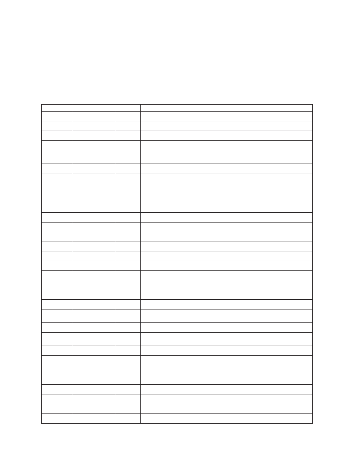
Item Code No. Parts Name Specification Q R
MA1M PCB
1 6925 8890 PCB/ASSY (MA1M) M240676*1 1 A
LSI1 2012 5005 LSI,CPU GT913F(T) 1 A
LSI2 2012 4494 LSI,DSP HG51B277FB-1 1 A
LSI3 2012 5665 LSI/MASK-ROM MX23C1610MC-12CA64 1 A
LSI4/LSI5 2012 5572 LSI/S-RAM TC55257DFL-70L(EL) 2 A
IC1 2105 4746 LSI/D/A CONVERTER UPD6379GR-E1 1 A
IC2 2012 1883 IC/MOS RN5VD40AA-TR 1 A
X1 2590 2699 OSCILLATOR/CERAMIC EFO-B2005E0 1 A
X2 2590 2700 OSCILLATOR/CRYSTAL XA10412 1 A
MA2M PCB
2 6925 8920 PCB/ASSY (MA2M) M140624*1 1 B
IC301 2114 1883 IC/LINEAR LA4620 1 A
IC302
Q301, Q306 2251 0672 TRANSISTOR 2SB1548-P.CS 2
Q302/304
Q307-Q312
Q303 2251 0910 TRANSISTOR 2SB1237Q,R-TV2-T 1 A
Q307 2360 1085 DIODE/ZENER HZS6B1LTD-T 1 A
D301/302 2390 1463
D303 - D306
D308/311
D310 2360 2233 DIODE/ZENER RD5.1JSB1-T1-T 1 A
J301
J302 3612 0665 JACK YKB21-5006 1 B
J303 3612 0789
J304 3501 4816
3 6925 8950 BL ASSY M240682*1 1
4 6925 8960 PCB/ASSY (LCD1M) M240678*1 1
5 3122 3524 LAMP,FLORESCENT HMBV26BAG63N/AZ 1
6 5861 3522 CUSHION/LAMP HRB-0256 2
LSI501 2012 5569 LSI/LCD DRIVER SED1278F0A 1
Q501/502 2253 0710
Q503 2250 1577
Q504 2220 1409
D501 2360 3056 DIODE/ZENER HZS6A2LTD-T 1
D502 2390 1344 DIODE 1SS133T-77-T 1
C501 2830 9236 MYLAR CAPACITOR NNMTP104K50-T 1
L501 3841 1197 COIL LHL08TB101K 1 C
T501 3012 1470 TRANS/INVERTER NT-07 1
VR501 2775 0994 POTENTIOMETER EVN-D8AA03B53 1
7 6925 8970 PCB/ASSY (CN1,2,3,4) M140606*1 1 B
D601 2360 1729
D602 - D644 2390 1344
LED601 2370 0343 LED LN28RPX-(TT) 1 C
VR601 2765 2178 POTENTIOMETER EWASC2C95B23 1 B
8 6925 8930
D809 - D946 2390 1344
9 6925 8940
D801 - D808 2390 1344
2114 1421 IC/PHOTO COUPLER PC900V 1
2252 0154 TRANSISTOR 2SC1740SS-TP-T 8 B
DIODE,SHOTTKY
2390 1344
3501 5012 JACK/POWER HEC2305-01-920 1 B
BL ass'y
CN1 ~ CN4 PCBs
KY PCBs
DIODE
JACK
JACK/DIN
TRANSISTOR
TRANSISTOR
TRANSISTOR
DIODE/ZENER
DIODE
PCB/ASSY (KY1,2)
DIODE
PCB/ASSY (KY3)
DIODE
SB20-03B 2 B
1SS133T-77-T 6 B
YKB21-5010 1 B
YKF51-5051 1 B
2SD965-R(TA) 2
2SA933ASTPR 1
2SC1740SR-TP-T 1
MTZJ5.1AT-77-T 1 B
1SS133T-77-T 43 C
M140614*1 1 B
1SS133T-77-T 138 B
M340666*1 1 B
1SS133T-77-T 8 B
B
B
B
B
A
B
A
B
B
B
B
B
C
B
B
Notes: Q – Quantity per unit
R – Rank
— 23 —
Page 24

Item Code No. Part Name Specification Q R
Keyboard
10 6922 2720
11 6922 2730
12 6906 8481
13 6926 2500
14 6926 2510
KEY SET/LT WHITE
KEY SET/LT WHITE
KEYSET/BLACK 10P
RUBBER/CONTACT
RUBBER/CONTACT
M312118*1 5 A
M312118*2 1 A
M140369A-3 3 A
M240699-2 5 A
M240700-2 1 A
Bender
15 2765 1141
16 6906 8492
17 6911 5261
POTENTIOMETER
KNOB/BEND
SPRING/BENDER
RK1631110-50KB 1 B
M31488B-4 1 B
M41949A-1 1 C
Panel
18 3831 1074 SPEAKER S12J82A 2
19 3831 1075 SPEAKER S05JH37A 2 B
20 3335 6571 LCD LD-B10060E 1
21 6909 5890 SWITCH/SLIDE KNOB CSB-12D 1 B
22
6921 5031 KNOB M311859A-1 2 B
23 6925 9380 RUBBER/BUTTON M240641-1 1
24
25 6925 9400
26
6925 9390 RUBBER/BUTTON M240636-1 1 B
RUBBER/BUTTON
M240638-1 1 B
6925 9410 RUBBER/BUTTON M240640-1 1 B
27 6925 9420 RUBBER/BUTTON M240640-2 1 B
28 6925 9430 RUBBER/BUTTON M240635-1 2
29 6925 9440 RUBBER/BUTTON M240639-1 1 B
30
6925 9450
RUBBER/BUTTON
M240634-1 1 B
31 6925 9460 RUBBER/BUTTON M240632-1 1 B
32
6925 9470
RUBBER/BUTTON
M240633-1 1 B
33 6926 2540 RUBBER/INTERCONNECTOR M440459-2 2 B
34 6925 9340 PANEL/DISPLAY M340642-1 1
35 6906 8456 COVER/BATTERY M311164F*12 1 B
Accessory
6925 9770 STAND/NOTE M140586-1 1
B
A
B
B
C
B
Notes: Q – Quantity per unit
R – Rank
— 24 —
Page 25

MA0700571A
8-11-10, Nishi-Shinjuku
Shinjuku-ku, Tokyo 160, Japan
Telephone: 03-3347-4926
 Loading...