

Page 1
CT-X870IN / VER.2
DISASSEMBLY
1. Precautions
Y
About repair
• The fi gures in this chapter show a prototype, so the appearance of parts may slightly diff er from the
actual parts.
• To avoid damages to the instrument and fl oor, lay the instrument on a mattress or blanket before
starting disassembling.
• There are several kinds of screws. Be sure to use the correct type of screws when assembling.
It is advisable to sort the screws as shown below after removing them.
• If a screw cap is attached to the screw, remove it.
When assembling, reattach the screw cap.
• Check how cables are wired before removing cables.
When assembling, wire the cables in the same manner as they were before disassembly.
• If a cable is bound by cable tie, tape or similar item, remove it as necessary.
When assembling, bind the cable as it was before disassembly.
• The number of pins of ribbon cable is sometimes diff erent from the number of pads of PCB.
Solder the pin No. 1 (orange) of cable on the pad No. 1 of PCB.
Y
Before starting repair or servicing
• Remove the AC adaptor, AC cord or batteries.
• Remove accessories such as the music stand.
– 1 –
Page 2
2. Disassembly Procedure
Y
Flowchart
Assembled Product
A. Case
B. Main Panel
C. Side Panel
F. BENDER-UNIT
G. SPEAKER
CT-X870IN / VER.2
D. PCB UNIT/MAIN
E. BACK LIGHT UNIT Disassembly of the Backlight Block
H. KEY
I. PCB UNIT/KEYBOARD/KYA
– 2 –
Page 3
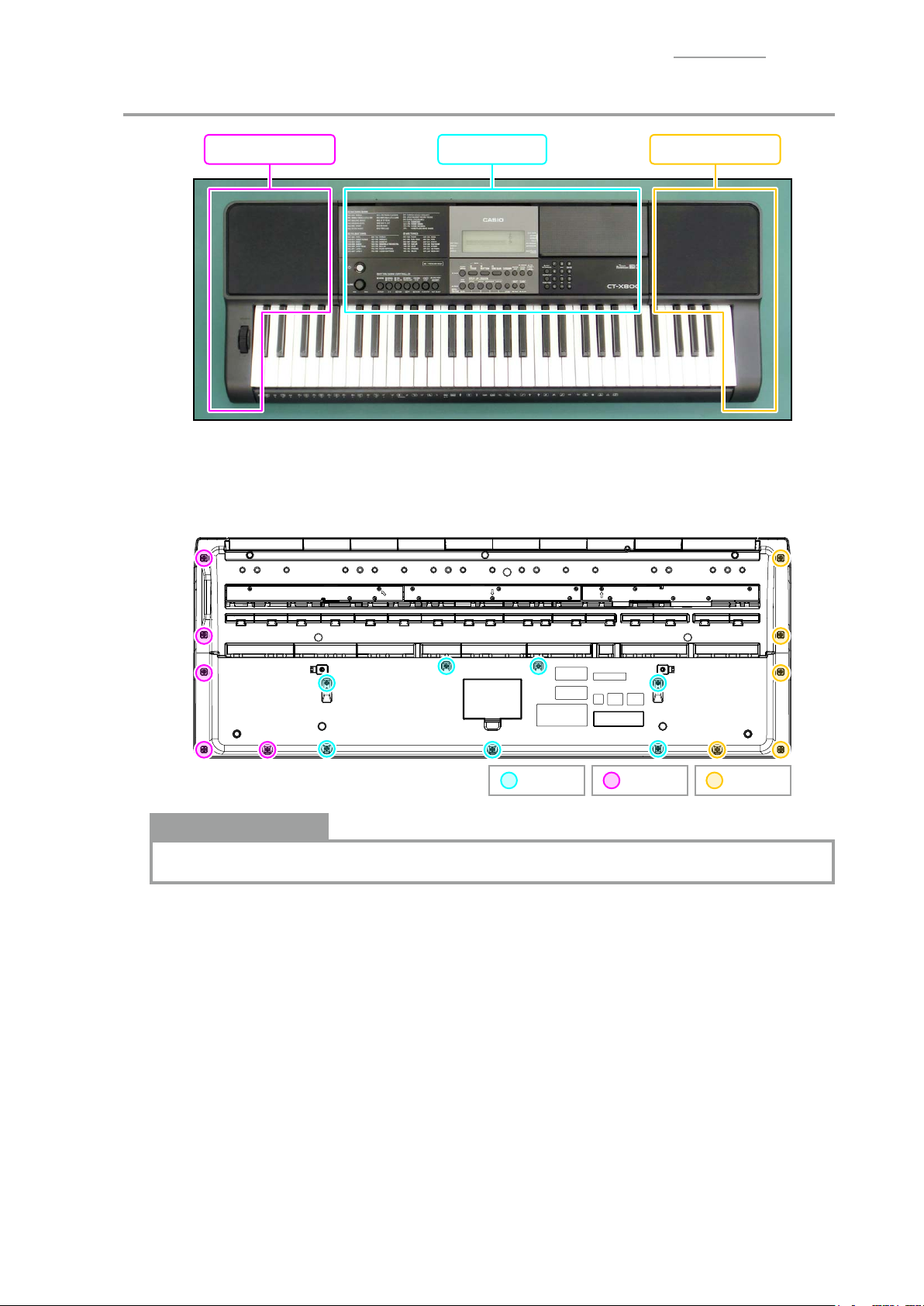
A. Removing the Case
A-1. Undo screws on the bottom surface.
• To remove the main panel, undo 7 screw A.
• To remove the left side panel, undo 7 screw A and 5 screw B.
• To remove the right side panel, undo 7 screw A and 5 screw C.
CT-X870IN / VER.2
Right side panelLeft side panel Main panel
Notes on Assembly
• Check that cables are not covering the screw hole before tightening a screw.
: Screw C : Screw B : Screw A
– 3 –
Page 4
CT-X870IN / VER.2
A-2. Place the digital keyboard with the keyboard facing up.
NOTE: The panel(s) and lower case are not secured at this point.
Hold the panel(s) with your hands when turning over the digital keyboard.
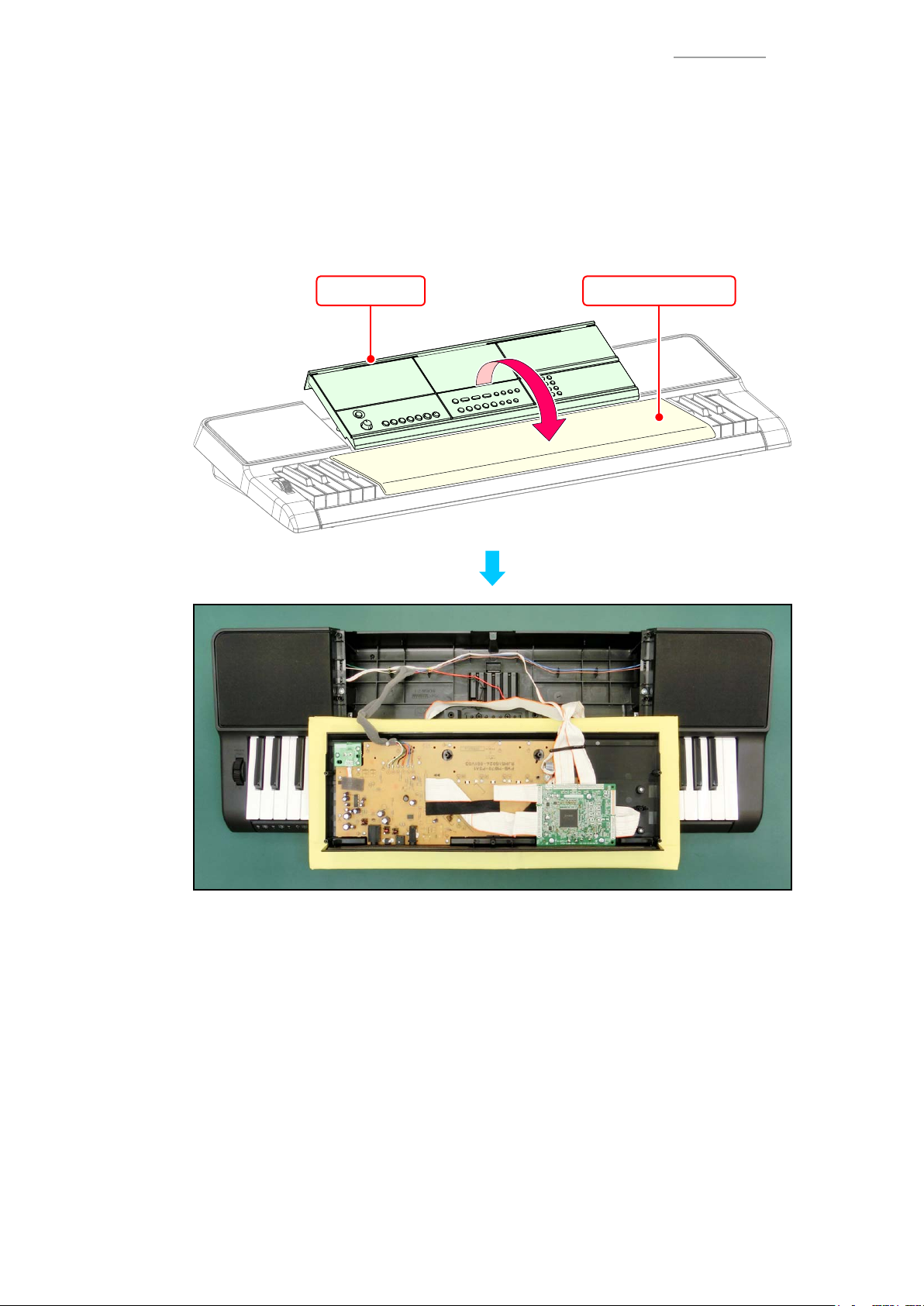
A-3. Lift the main panel and turn it over.
NOTE: The main panel and lower case are connected with cables. Use caution so as not to
apply too much tension to the cables when lifting the main panel.
NOTE: Mat a cushion material (cloth etc.) not to damage the keyboard before placing the
main panel.
Main panel Cushion material
– 4 –
Page 5
CT-X870IN / VER.2
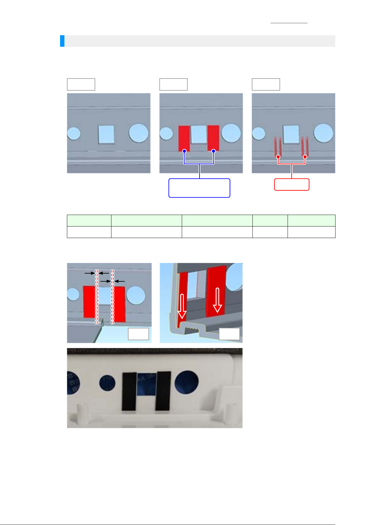
Checking the Main Panel Type and Attaching the Spacer
• There are three types of the power terminal opening (on the reverse side) of the main panel.
For Type A, attach the spacer (SHEET/V-ZERO) the same way as Type B.
No spacer is necessary for Type C.
Type A Type B Type C
Spacer
Rib
(SHEET/V-ZERO)
<Spacer Position>
Code No. Parts Name Specifi cation Q’ty Remarks
10609381 SHEET/V-ZERO RJM517844-001V01 2 Black
• Fig. 1: Attach the spacer at 0 to 1.0 mm from the edge of the terminal opening.
• Fig. 2: Position the spacer against the bottom surface of the lower case.
Fig. 1 Fig. 2
– 5 –
Page 6
CT-X870IN / VER.2
Notes on Assembly
• When any of lead wires is replaced, arrange the lead wires to the rib of lower case and
bundle the 6 lead wires with SPONGE/50X260.
* For the affi xing position of sponge, refer to the rib of lower case shown in the fi gure below.
Rib
SPONGE/50X260
• Before assembling the main panel, check the knot of cable tie that fi xes lead wires to PSA1
PCB is in the correct direction.
– The knot should be laterally facing the PCB.
* If the main panel is closed while the knot faces upward, it interferes with the keyboard
and the main panel may fl oat.
• Fig. 1: Before assembling the main panel, arrange ribbon cables (x3) as shown in the fi gure
below and bundle them with a cable tie.
Fold and tuck an excess length of the pitch bend cable under the KYA PCB cable
Hold the ribbon cables with a clip
Fold the ribbon cables upward (approx. 90 degrees)
• Fig. 2: When assembling the main panel, hold the cables shown in the red frame in the fi gure
below by hand and close the main panel.
Fig. 1 Fig. 2
: Cable tie
– 6 –
Page 7
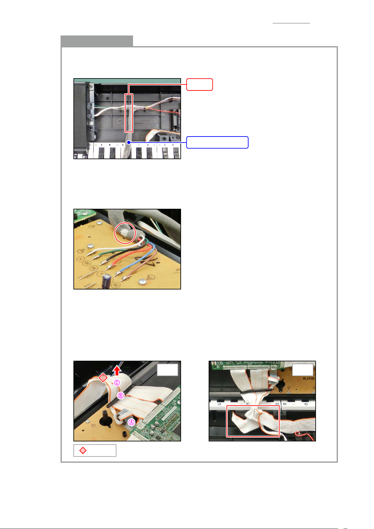
B. Removing the Main Panel
B-1. Unsolder to disconnect the following cables and remove the main panel.
NOTE: Release the ribbon cables from the clip.
MEMO: The lead wires are fi xed to the hole of PSA1 PCB with a cable tie.
Cable / Remarks Connected From
CT-X870IN / VER.2
: Cable tie
2 lead wires From the left: White, green Left speaker
2 lead wires From the left: Black, red Battery springs
2 lead wires From the left: Blue, brown Right speaker
Ribbon cable 3-pin Pitch bend
Ribbon cable 13-pin (PCB: 14 pads) KYA1 PCB
Ribbon cable 11-pin (PCB: 15 pads) KYA2 PCB
Clip
– 7 –
Page 8
CT-X870IN / VER.2
C. Removing the Side Panel
C-1. Undo 2 screws (S4).
C-2. Remove the side panel cables from the rib of lower case and remove left side panel or right
side panel.
To completely remove the side panel, refer to the next page.
: S4 : Rib
– 8 –
Page 9

Y
Left Side Panel
(1) Unsolder to disconnect the following cables.
NOTE: Release the cables from the cable tie and clip.
NOTE: Remove the cables from the rib of lower case.
MEMO: The lead wires are bundled with sponge tape.
(2) Undo 1 screw and remove the FERRITE CORE.
Cable / Remarks Connected From
CT-X870IN / VER.2
2 lead wires From the left: White, green PSA1 PCB
Ribbon cable 3-pin MDA1 PCB
: Cable tie
Y
Right Side Panel
(1) Unsolder to disconnect the following cable.
NOTE: Remove the cable from the rib of lower case.
MEMO: The lead wires are bundled with sponge tape.
FERRITE CORE Clip
: Cable tie : Screw
: Cable tie
Cable / Remarks Connected From
2 lead wires From the left: Blue, brown PSA1 PCB
– 9 –
Page 10
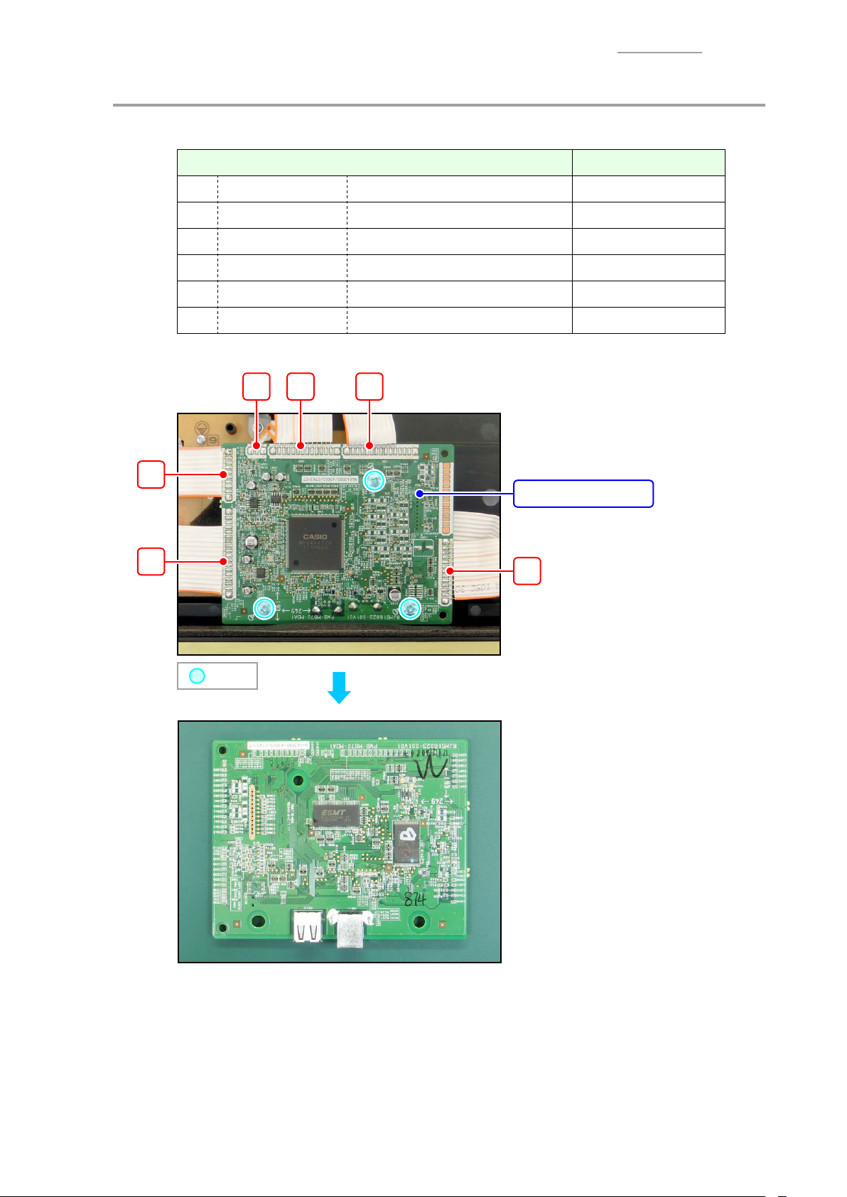
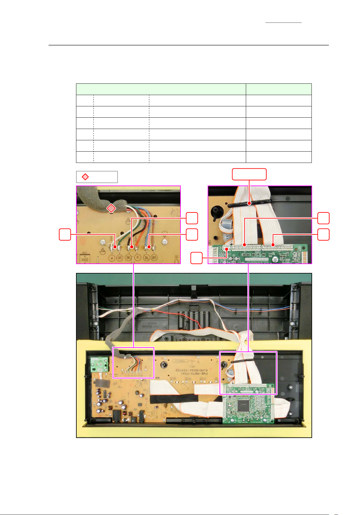
D. Removing the PCB UNIT/MAIN
D-1. Unsolder to disconnect the following cables.
Cable / Remarks Connected From
CT-X870IN / VER.2
D-2. Undo 3 screws and remove the PCB UNIT/MAIN.
Ribbon cable 3-pin Pitch bend
Ribbon cable 13-pin (PCB: 14 pads) KYA1 PCB
Ribbon cable 11-pin (PCB: 15 pads) KYA2 PCB
Ribbon cable 10-pin PSA1 PCB
Ribbon cable 15-pin (PCB: 18 pads) PSA1 PCB
Ribbon cable 13-pin PSA1 PCB
PCB UNIT/MAIN
: Screw
– 10 –
Page 11

CT-X870IN / VER.2
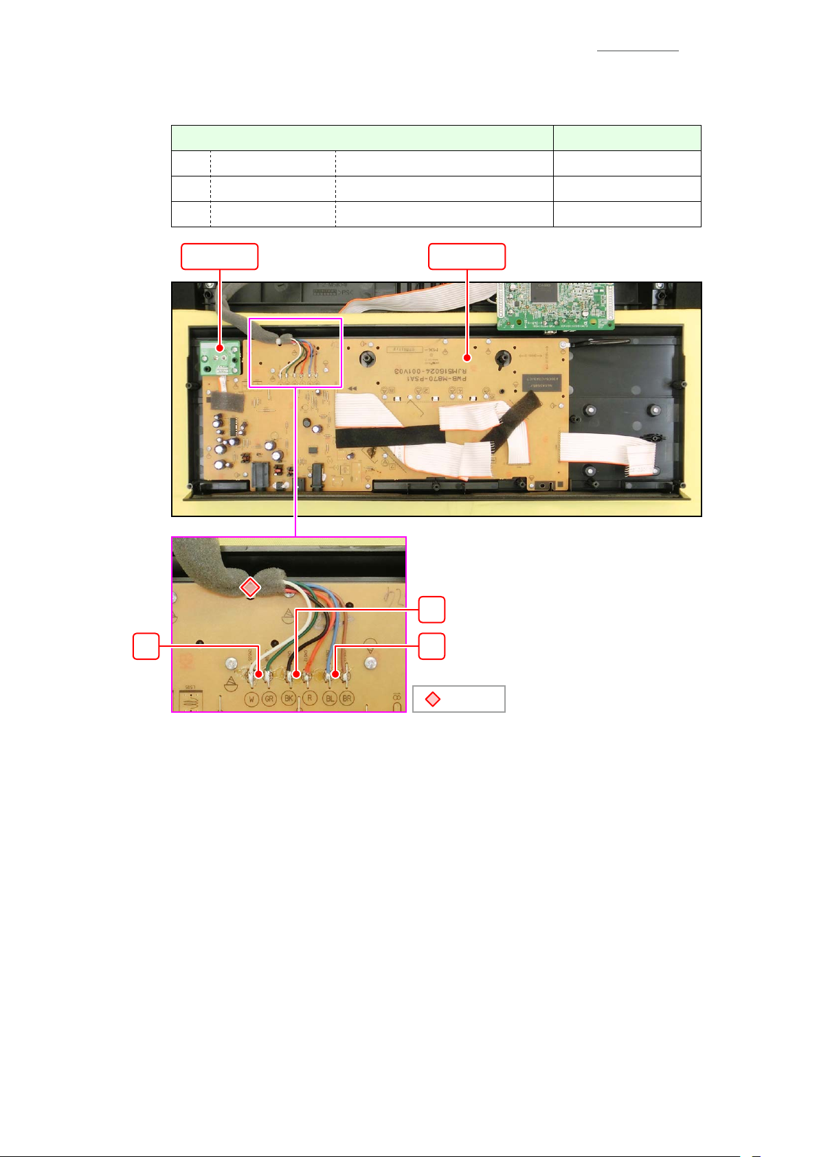
E. Removing the BACK LIGHT UNIT
MEMO: BACK LIGHT UNIT is confi gured with PSA1 PCB, PSA2 PCB, and backlight component.
E-1. Unsolder to disconnect the following cables.
NOTE: Release the cables from the clip.
MEMO: BACK LIGHT UNIT (PSA1 PCB, PSA2 PCB) can be removed without disconnecting
cable
, and cable , and cable .
Cable / Remarks Connected From
E-2. Undo 3 screw A and 1 screw B, and then remove the MDA1 PCB and FERRITE CORE (for
cable
FERRITE CORE
Ribbon cable 10-pin PSA1 PCB
Ribbon cable 15-pin (PCB: 18 pads) PSA1 PCB
Ribbon cable 13-pin PSA1 PCB
) from the PSA1 PCB.
Clip
MDA1
: Screw A : Screw B
– 11 –
Page 12
E-3. Unsolder to disconnect the following cables.
MEMO: The lead wires are fi xed to the hole of PSA1 PCB with a cable tie.
Cable / Remarks Connected From
CT-X870IN / VER.2
2 lead wires From the left: White, green Left speaker
2 lead wires From the left: Black, red Battery springs
2 lead wires From the left: Blue, brown Right speaker
PSA2 PSA1
: Cable tie
– 12 –
Page 13
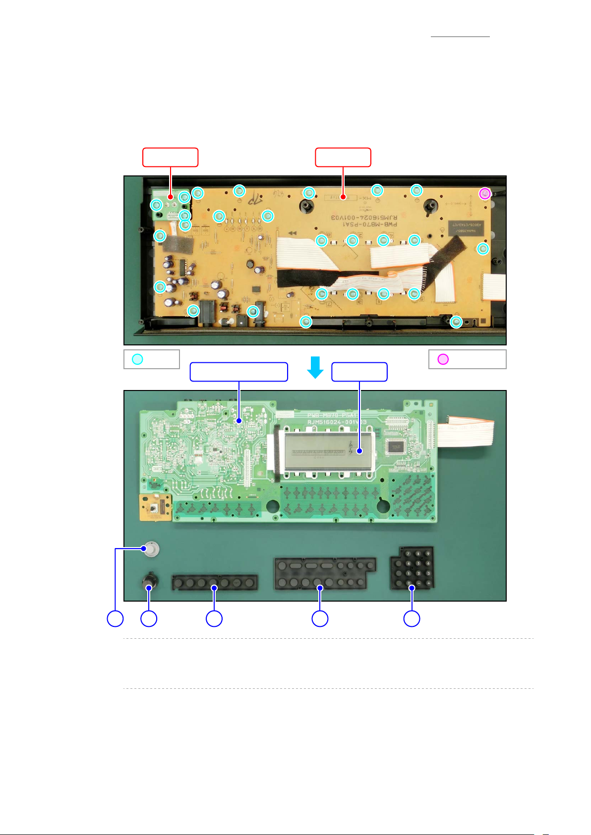
CT-X870IN / VER.2
E-4. Undo 27 screws and then remove the BACK LIGHT UNIT (w/ FABRIC TAPE, PACKING,
KNOB, SPONGE (2 sheets)) , rubber keys (4 pcs.), and LCD.
MEMO: One screw is tightened with the clip.
NOTE: The LCD may be stuck on the BACK LIGHT UNIT.
Use caution when handling the BACK LIGHT UNIT to prevent the LCD from dropping.
E-5. Remove the KNOB from the PSA2 PCB.
PSA2 PSA1
: Screw
: Screw / Clip
LCDBACK LIGHT UNIT
A
D ECB
A: RUBBER BUTTON/A (for Power button)
B: KNOB
C: RUBBER BUTTON/A
– 13 –
D: RUBBER BUTTON/B
E: RUBBER BUTTON/C
Page 14
CT-X870IN / VER.2
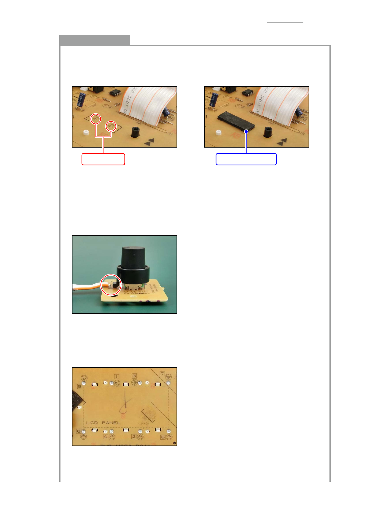
Notes on Assembly
• When replacing the BACK LIGHT UNIT, attach PACKING/10X30 to PSA1 PCB as shown in
the fi gure below.
* Attach tha packing in accordance with silk-printed solid line (square bracket x2).
– For protect the ribbon cable from lead frame of backlight LED protruding from PCB
PACKING/10X30Lead frame
• When attaching the KNOB, push it to the back surely.
– The gap between knob (convex part) and PCB should be less than 1 mm
Reference: When setting the nob to max. sound volume, min. sound volume, or medium
sound volume position, 1 mm gap gauge should not be inserted at each position.
• Before assembling the BACK LIGHT UNIT, check the ribbon cable of PSA2 PCB is parallel to
the PCB.
* If the ribbon cable is fl oating, it may interfere with the rotation of knob.
• Before assembling the LCD, check that the LCD surfaces on the main panel side and LCD
side are free from dust and dirt.
• Be sure that the LCD is in the correct orientation when assembling.
• Tighten the screws at LCD part in the silk-printed order.
If not tightened correctly, it may cause LCD display errors.
– 14 –
Page 15

CT-X870IN / VER.2
• Arrange the ribbon cables of PSA1 PCB as shown in the fi gure below and fi x them with
sponge or fabric tape.
3-pin ribbon cable:
– Carry out the wire arrangement in such a way to fold the cable
– Fix the cable with SPONGE/20X40
* For the affi xing position of sponge, refer to the silk-printed solid line (square bracket)
* The sponge should not exist on the screw.
15-pin ribbon cable:
– Mountain-fold the cable in accordance with silk-printed dashed line (2 positions)
– Fix the cable with FABRIC TAPE/20X120
* For the affi xing position of fabric tape, refer to the edge surface of cable
10-pin ribbon cable:
– Accordion-fold the cable in accordance with silk-printed dashed line
– Fix the cable with SPONGE/20X80
* For the affi xing position of sponge, refer to the silk-printed solid line (center of 2 square
brackets).
* The sponge should not exist on the screw, screw hole (for ferrite core) and boss.
: Screw hole : Boss : Screw
– 15 –
Page 16

CT-X870IN / VER.2
Y
Disassembly of the Backlight Block
(1) Remove the LCD (A).
(2) Peel off the SPONGE/8X75 (B), and then remove the TOP PIECE (C), FILM (D), BACK LIGHT
PLATE (E), and RUBBER CONNECTOR (2 pcs, F).
(3) Unhook the hook on the back surface of PSA1 PCB and remove the REFLECTOR (G).
NOTE: When removing the REFLECTOR, check hook and boss of REFLECTOR are
disengaged from the PCB.
NOTE: Remove the REFLECTOR not to apply load to LED as much as possible.
If the LED is bended, push the LED softly to adjust the position after the REFLECTOR
is attached.
B
C
A
D
: Hook : Boss
E
F
LED
G
LED
– 16 –
Page 17

F. Removing the BENDER UNIT
F-1. Unsolder to disconnect the following cable.
Cable / Remarks Connected From
CT-X870IN / VER.2
Ribbon cable 3-pin MDA1 PCB
F-2. Undo 1 screw and remove the FERRITE CORE.
NOTE: Release the pitch bend cable from the cable tie and clip.
FERRITE CORE
Clip
: Cable tie : Screw
F-3. Undo 2 screws and remove the BENDER UNIT (w/ FERRITE CORE).
NOTE: Remove the pitch bend cable from the ribs of lower case and side panel.
BENDER UNIT
: Screw
: Boss
FERRITE CORE
– 17 –
Page 18

CT-X870IN / VER.2
Notes on Assembly
• When replacing the BENDER UNIT, attach the FERRITE CORE to the cable as shown in the
fi gure above ( = 80mm).
* Wrap the cable around the FERRITE CORE once
• Arrange the pitch bend cable on the outside of the boss as shown in the fi gure above.
* The pitch bend cable, if arranged inside the boss, may interfere with the rotation of the pitch
bend
G. Removing the SPEAKER
G-1. Unsolder to disconnect the following cable.
NOTE: Remove the speaker cable from the ribs of lower case as necessary.
Cable / Remarks Connected From
G-2. Undo 4 screws and remove the SPEAKER.
<Left speaker> <Right speaker>
2 lead wires From the above: White, green PSA1 PCB
2 lead wires From the above: Brown, blue PSA1 PCB
: Screw : Screw
SPEAKER
Notes on Assembly
• Tighten the screws while pushing the speaker toward the arrow shown in the fi gure above.
– 18 –
Page 19

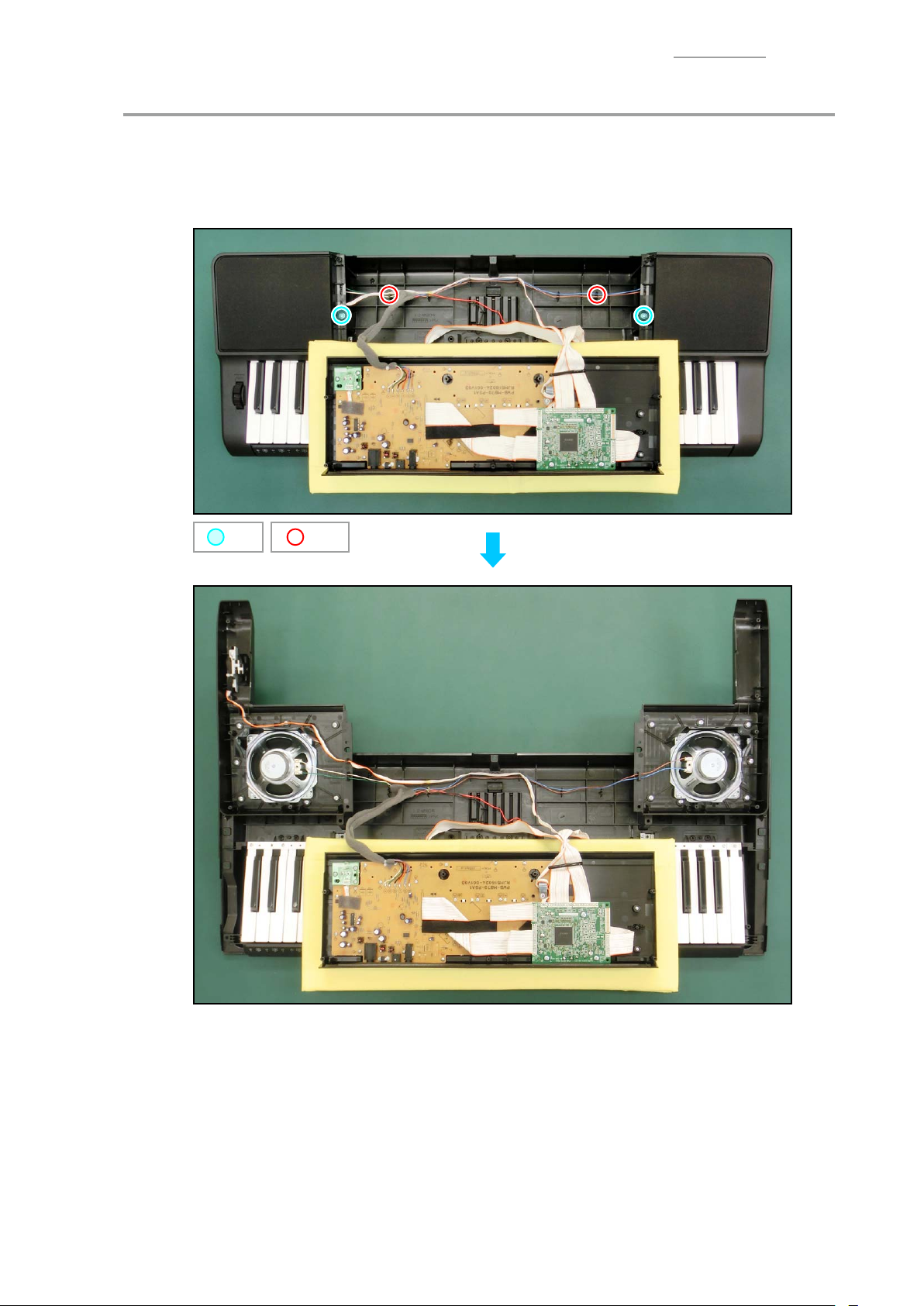
H. Removing the KEY
H-1. Remove the main panel, left side panel, and right side panel.
For disassembly procedure, refer to the applicable section.
H-2. Undo 21 screws and then remove the WHITE KEY and BLACK KEY.
NOTE: When removing the KYA PCB, untie the KYA PCB cables (x2) and pitch bend cable.
CT-X870IN / VER.2
: Screw : Cable tie
Notes on Assembly
• After assembling the KEY, press the keys to check that the keys move smoothly.
– 19 –
Page 20

CT-X870IN / VER.2
I. Removing the PCB UNIT/KEYBOARD/KYA
I-1. Unhook and remove the PCB UNIT/KEYBOARD/KYA (w/ RUBBER CONTACT/CB, RUBBER
CONTACT/CS).
I-2. Remove 4 RUBBER CONTACT/CB and RUBBER CONTACT/CS.
MEMO: The RUBBER CONTACT/CS diff ers from the others in length.
: Hook
PCB UNIT/KEYBOARD/KYA
KYA1 KYA2
Notes on Assembly
• To install the RUBBER CONTACT, lightly insert the
tip of a rubber into the PCB fi rst, and then press it in
using the end of a paper clip.
* Do not press with too much force. Doing so may
damage the rubber.
RUBBER CONTACT/CSRUBBER CONTACT/CB
– 20 –
Page 21

• Arrange the KYA PCB cables as shown in the fi gure below.
Fold the edge of the cable toward the back
* The cable should not be higher than the PCB surface
Fold in half
CT-X870IN / VER.2
– 21 –
Page 22

CT-X870IN / VER.1
FUNCTION TEST
1. Overview
Y
Test Items
To test this product, fi rst launch the built-in diagnostic program, and then perform the following tests in
sequence.
No. Item Necessary Items
A Button Test –
B Pitch Bend Test –
C LCD Test –
D Model Test –
E ROM Version Check –
F Pedal Test SP-3 or SP-20 pedal (sold separately)
G USB Test PC, USB cable
H USB Flash Drive Test USB fl ash drive
I RAM Test –
MEMO: Testing requires the AC adaptor or 6 AA-size dry batteries with enough capacity.
MEMO: For information about PC system requirements, refer to the User’s Guide.
MEMO: Be sure to use a USB fl ash drive formatted by the digital keyboard system.
For how to format the USB f ash drive, refer to the User’s Guide.
Y
Launching the Diagnostic Program
(1) Connect the AC adaptor or load the 6 AA-size dry batteries.
(2) Adjust the sound volume so that it is at about 1/3 of the full volume.
(3) While holding down [0], [1], and [3] buttons, turn on the power.
When the diagnostic program is launched, “SW” or “SW : 22” appears.
MEMO: If the buttons are pressed long, “SW: 22” may appear.
NOTE: Be sure to turn off the power when the test is fi nished.
To turn off the power, hold down [P] button until the screen shuts down.
– 1 –
Page 23

2. Test Procedure
A. Button Test
NOTE: Check there is no uncomfortable feeling when pressing the button.
If the button gets lodged or does not return to the correct position, evaluate the test as NG.
A-1. Press the buttons in the sequence to check that the keys operate properly.
For the button sequence, refer to the following fi gure.
• OK: The confi rmation tone (cowbell) sounds, and “SW :” and “button number (XX)” appear.
When press the last button, the completion tone sounds, and “OK :” and “button
number (XX)” appear.
• NG: If the buttons are pressed in a wrong sequence, the error tone sounds, and “SW :” and
“button number (XX)” appear.
CT-X870IN / VER.1
Button number
<Sequence of the button to press / Button number>
START
167 146 147 148 111 108
121 122 123 124 125 130
80 82 83 88 90 91 92
93 64
50 52
62 23 24 25
170
10 19 13 12
END
26 27 28
20 21 22
A-2. Check that the following screen appears when you press the last button in the sequence.
– 2 –
Page 24

CT-X870IN / VER.1
B. Pitch Bend Test
NOTE: Check that the pitch bend wheel rotates smoothly.
If you feel a catch in the pitch bend wheel or it does not rotate smoothly, evaluate the test
as NG.
B-1. Press [0] button to display the following screen.
B-2. Rotate the pitch bend wheel all the way up, and check that the following screen appears.
MEMO: The confi rmation tone (cowbell) sounds.
B-3. Return the pitch bend wheel to the original position.
B-4. Rotate the pitch bend wheel all the way down, and check that the following screen appears.
MEMO: The confi rmation tone (cowbell) sounds.
B-5. Return the pitch bend wheel to the original position, and check that the following screen
appears.
MEMO: The confi rmation tone (triangle) sounds.
– 3 –
Page 25

C. LCD Test
C-1. Press [0] button to display the following screen.
C-2. Press [0] button and check that all segments are lit.
C-3. Press [0] button and check that all segments are turned off .
CT-X870IN / VER.1
D. Model Test
D-1. Press [0] button to display the following screen.
D-2. Press [0] button and check that the model name is “MX874B”.
– 4 –
Page 26

E. ROM Version Check (This item is not an inspection)
E-1. Press [0] button to display the ROM version.
NOTE: The displayed ROM version may diff er depending on the individual products.
(The fi gure shown below indicates an example of display)
F. Pedal Test
NOTE: This test cannot be performed without a pedal.
F-1. Press [0] button to display the following screen.
CT-X870IN / VER.1
F-2. Connect the pedal to the PEDAL jack.
F-3. Press the pedal and check that the following screen appears.
F-4. Release the pedal and check that the following screen appears.
– 5 –
Page 27

CT-X870IN / VER.1
G. USB Test
NOTE: This test cannot be performed without a PC and USB cable.
G-1. Connect the USB port of digital keyboard and PC with a USB cable, and then check that the
following screen appears.
G-2. Disconnect the USB cable from the digital keyboard and check that the following screen.
H. USB Flash Drive Test
NOTE: This test cannot be performed without a USB fl ash drive.
H-1. Insert a USB fl ash drive into the USB fl ash drive port and check that the following screen.
H-2. Press [0] button to display the following screen.
H-3. Press [0] button to begin the test and check that the screen changes as fi gure below.
– 6 –
Page 28

CT-X870IN / VER.1
H-4. Remove the USB fl ash drive from the digital keyboard and check that the following screen.
– 7 –
Page 29

I. RAM Test
I-1. Press [0] button to display the following screen.
I-2. Press [0] button to begin the test.
I-3. Check that the following screen.
CT-X870IN / VER.1
I-4. Turn off the power by holding down [P] button until the screen shuts down.
– 8 –
Page 30

BLOCK AND WIRING DIAGRAM
CT-X870IN / VER.1
Keyboard PCB (KYA1)
CN801 (13-pin)
Main PCB
(MDA1)
VD5
Power Supply
Circuit
IC4, IC5
RESETB
CN5 (13-pin)
FI0-FI3,
KC0-KC4,
SI0-SI3
VD1.2
VD3
VDA3
CN803 (10-pin)
CN802 (10-pin)
CN804 (11-pin)
CN6 (11-pin)
DDR2 SDRAM
IC2
EEPROM
IC3
Keyboard PCB (KYA2)
KC5-KC7,
FI4-FI7,
SI4-SI7
MA0-MA12
MD0-MD15
NFD0-NFD7
MPU
IC1
USB-A
(CN10)
PITCH BEND
USB-B
(CN11)
CN12 (3-pin)
CN22 (13-pin)
CN523 (13-pin)
Button
Power Amp PCB
(PSA1)
KC0-KC7,
KI0-KI2,
SFI0, SF1
CN517
LCD
CN518
PWM, RS,
R/W, E,
DB4-DB7
CN30 (10-pin)
CN519 (10-pin)
LCD
Controller
IC506
PWSW
Power switch
VCP
APO
Power Supply
Circuit
IC504
Filter
IC7
VD5 VA5
LOUT ROUT
CN14 (15-pin)
CN521 (15-pin)
PEDAL
BATT SP_MUTE
VA3
VD5
VA5
VE5
VCP
GND GND GND
CN511
CN512
SPMUTE
CN505CN508
Power
Amplifier
IC501
LLR
R
CN513CN514
ADC
IC11
AUDIO_IN_L AUDIO_IN_R VOL
Filter
IC502
LR
VVOL
(VDA3)
CN504 (3-pin)
CN601 (3-pin)
VOLUME
(VR601)
Volume PCB
(PSA2)
Battery
– 1 –
DC
(J502)
PEDAL
(J504)
SPEAKER (L)
PHONES
(J501)
AUDIO IN
(J503)
SPEAKER (R)
Page 31

CIRCUIT DESCRIPTION
Y
Nomenclature of Keys
Y
Key Matrix
Each key has two contacts, the fi rst contact and second contact .
NOTE: The diagram below illustrates how the contacts work.
CT-X870IN / VER.1
KC0 KC1 KC2 KC3 KC4 KC5 KC6 KC7
FI0 C2
SI0 C2
FI1 G2#
SI1 G2#
FI2 E3
SI2 E3
FI3 C4
SI3 C4
FI4 G4#
Second contact
C2#
C2#
A2
A2
F3
F3
C4#
C4#
A4
D2
D2
A2#
A2#
F3#
F3#
D4
D4
A4#
Key
D2#
D2#
B2
B2
G3
G3
D4#
D4#
B4
First contact
E2
E2
C3
C3
G3#
G3#
E4
E4
C5
F2
F2
C3#
C3#
A3
A3
F4
F4
C5#
FI
KC
SI
F2#
F2#
D3
D3
A3#
A3#
F4#
F4#
D5
G2
G2
D3#
D3#
B3
B3
G4
G4
D5#
SI4 G4#
FI5 E5
SI5 E5
FI6 C6
SI6 C6
FI7 G6#
SI7 G6#
A4
F5
F5
C6#
C6#
A6
A6
A4#
F5#
F5#
D6
D6
A6#
A6#
B4
G5
G5
D6#
D6#
B6
B6
– 2 –
C5
G5#
G5#
E6
E6
C7
C7
C5#
A5
A5
F6
F6
D5
A5#
A5#
F6#
F6#
D5#
B5
B5
G6
G6
Page 32

Y
Button Matrix
CT-X870IN / VER.1
KI0 KI1 KI2 SFI0 SFI1
KC0
[ACCOMP],
KC1 TONE
KC2
KC3
KC4
KC5
KC6 TEMPO/TAP 0257
KC7 –3689
PIANO/ORGAN,
$
TOUCH
SPLIT,
$
POINT
Area 1,
LISTEN
METRONOME,
$
BEAT
PART SELECT,
$
MUSIC PRESET
CATEGORY SONG BANK RECORD/STOP RHYTHM
EASY MODE, BANK,
$
FREEZE
Area 2,
WATCH
+ FUNCTION 1 4
INTRO,
REPEAT
ENDING/
SYNCHRO START,
d
FF
LAYER,
$
OCTAVE
Area 3,
REMEMBER
VAR. FILL-IN,
s
REW
START/STOP,
PLAY/STOP
A.HAR./ARPEG.,
$
TYPE
Area 4,
PHRASE
NORMAL FILL-IN,
A-B
SYNCHRO STOP,
k
PAUSE
STORE
CHORD MODE,
$
CHORD BOOK
– 3 –
Page 33

Main PCB: M870-MDA1
CT-X870IN / VER.1
PRINTED CIRCUIT BOARDSPRINTED CIRCUIT BOARDS
– 4 –
Page 34

CT-X870IN / VER.1
Power Amp PCB: M870-PSA1 Volume PCB: M870-PSA2
– 5 –
Page 35

Keyboard PCB: M802-KYA1
CT-X870IN / VER.1
Keyboard PCB: M802-KYA2
– 6 –
Page 36

Main PCB: M870-MDA1 (1/2)
CT-X870IN / VER.1
SCHEMATIC DIAGRAMS
Î PSA1/CN519
USB-B
(CN11)
USB-A
(CN10)
Î PSA1/CN523
KYA1/CN801 Í
KYA2/CN804 Í
Not used
– 7 –
Page 37

Main PCB: M870-MDA1 (2/2)
CT-X870IN / VER.1
Î PSA1/CN521
Not used
– 8 –
Page 38

Power Amp PCB: M870-PSA1 (1/2)
CT-X870IN / VER.1
PHONES
(J501)
DC
(J502)
AUDIO IN
(J503)
PEDAL
(J504)
Î PSA2/CN601
Î SPEAKR (L)
Î BATTERY
Î MDA1/CN14
Î SPEAKR (R)
SPEAKR (L)
BATTERY
SPEAKR (R)
Not used
– 9 –
Page 39

Power Amp PCB: M870-PSA1 (2/2) Volume PCB: M870-PSA2
Î MDA1/CN30
CT-X870IN / VER.1
VOLUME
(VR601)
Î LCD
Î LCD
Î MDA1/CN22
Î PSA1/CN504
– 10 –
Not used
Page 40

Keyboard PCB: M802-KYA1
CT-X870IN / VER.1
Î MDA1/CN5 Î KYA2/CN803
– 11 –
Page 41

Keyboard PCB: M802-KYA2
CT-X870IN / VER.1
Î KYA1/CN802 Î MDA1/CN6
– 12 –
Page 42

CT-X870IN / VER.2
Main Unit
N 1 10568212 DISPLAY PLATE RJM516224-003V02 1 X
N 2 10563768 SPONGE/50X260 RJM516354-001V01 1 X for Wires
3 10517162 SCREW RJM514943-001V01 17 X
4 10521852 LOWER COVER/A RJM508655-001V05 1 X
5 10521853 LOWER COVER/B RJM508656-001V05 1 X
6 10521854 LOWER COVER/C RJM508657-001V05 1 X
S4 10203788 SCREW S-WLB0-4X10Z3NQ 2 X
Main Panel
N 7 10558735 PLATE RJM516106-002V01 1 X
N 8 10540407 FABRIC TAPE/5X45 RJM515372-001V01 3 X
N 9 10564562 CASE/PANEL RJM516103-004V01 1 X
10 10136565 PACKING/8X510 M441190-002V01 1 X
N 11 10563769 SHEET/V-ZERO RJM516425-001V01 1 X
12 69210550 FABRIC TAPE/5X13 M412026-1 2 X
N 13 10568196 SHEET/V-ZERO RJM516523-001V01 1 X
N 14 10567929 LCD UNC-LTNN014320-02 1 X
N 15 10558740 RUBBER BUTTON/C RJM516089-002V01 1 X
N 16 10558739 RUBBER BUTTON/B RJM516088-002V01 1 X
N 17 10558738 RUBBER BUTTON/A RJM516087-002V01 1 X
N 18 10564553 RUBBER BUTTON/A RJM511139-007V01 1 X Power button
19 10553264 KNOB/for ROTARY RJM515607-001V01 1 C
N 20 10566275 BACK LIGHT UNIT TK-RJM516205*003 1 X PSA1/PSA2
21 10270485 SPONGE/8X75 M441167-001V01 1 X
22 10131094 TOP PIECE RJM502565-001V01 1 X
N 23 10559870 FILM RJM516225-001V01 1 X
N 24 10557981 BACK LIGHT PLATE RJM516108-001V01 1 X
N 25 10559868 RUBBER CONNECTOR/for LCD RJM516226-001V01 2 X
N 26 10557978 REFLECTOR RJM516107-001V01 1 X
J502 10537493 JACK/DC KM02007P 1 A DC terminal
J501 10478582 JACK/PHONE PJ-64017A-PBTV0 1 B PHONES jack
J504 10490438 JACK/SUSTAIN PJ-64043B-PBTV0 1 C PEDAL jack
J503 10305131 JACK/AUDIO IN ST-3529B 1 B AUDIO IN jack
VR601 10554608 VARIABLE RESISTOR F-09KH1-CASIO-3 1 B Volume
27 10204256 FERRITE CORE TRCN16-13 1 X for Bender cable
28 10048978 SPONGE/20X80 M440721-1 1 X for Ribbon cable
29 10164446 FABRIC TAPE/20X120 RJM502073-002V01 1 X for Ribbon cable
30 10139463 PACKING/10X30 RJM503575-001V01 1 X for LED leads
31 10127790 SPONGE/20X40 RJM503059-001V02 1 X for Ribbon cable
N 32 10573314 PCB UNIT/MAIN TK-RJM516571*001 1 A MDA1
CN10 10432772 USB CONNECTOR (type A) UAR27-4K5J00 1 C USB-A port
CN11 10236624 USB CONNECTOR (type B) UBR24-4K5G00 1 C USB-B port
N 33 10517163 SCREW RJM514945-001V01 3 X
67 10609381 SHEET/V-ZERO RJM517844-001V01 2 B Spacer*
* For some models only (refer to DISASSEMBLY/ASSEMBLY Page 5)
R
Remarks
N
Item
Code No.
Parts Name
Specification
Q'ty
EXPLODED VIEW PARTS LIST
CT-X870IN_DI
1
S4
S4
2
47
43
45
2
x17
x17
3
3
6
6
5
5
34
35
36
x7
37
38
39
40
36
x4
42
44
x7
46
44
x4
48
4
4
41
* For some models only
(refer to DISASSEMBLY/ASSEMBLY page 5)
9
10
13
14
18
19
22
31
12
x3
30
67 x2
7
8
11
12
15
16
17
21
20
23
24
x2
25
26
28
27
29
33
32
x3
<Notes>
Price Code : Refer the latest “Parts Price Code” at “PARTS FINDER” on the Casio Service Website (https://www.servicecasio.com).
N : New parts
Q’ty : Quantity used per unit
R : Rank (A: Essential, B: Stock recommended, C: Others, X: No stock recommended)
– 1 –
Page 43

CT-X870IN / VER.2
R
Remarks
N
Item
Code No.
Parts Name
Specification
Q'ty
Right Panel
N 34 10566331 SPEAKER COVER/RIGHT RJM516119*002V02 1 X
N 35 10558742 SIDE PANEL/RIGHT RJM516105-002V01 1 X
N 36 10517163 SCREW RJM514945-001V01 11 X
N 37 10537088 FABRIC TAPE/20X10 M411742-004V01 1 X
38 10472328 SPEAKER CJ12FD02 1 X
39 10377007 W IRE 1007TASC24850B3030 1 X Blue
40 10377008 W IRE 1007TASC24850T3030 1 X Brown
Left Panel
N 41 10566329 SPEAKER COVER/LEFT RJM516118*002V02 1 X
N 42 10564563 SIDE PANEL/LEFT RJM516104-003V01 1 X
N 43 10566277 BENDER UNIT TK-RJM516439*001 1 C Pitch bend
N 44 10517163 SCREW RJM514945-001V01 11 X
N 45 10537088 FABRIC TAPE/20X10 M411742-004V01 1 X
46 10472328 SPEAKER CJ12FD02 1 X
N 47 10564948 W IRE 1007TASC24500W3030 1 X White
N 48 10564947 W IRE 1007TASC24500G3030 1 X Green
EXPLODED VIEW PARTS LIST
CT-X870IN_DI
1
S4
S4
67 x2
* For some models only
(refer to DISASSEMBLY/ASSEMBLY page 5)
2
2
7
8
x3
9
11
10
x17
x17
3
3
6
6
13
18
14
12
12
15
16
5
5
17
19
4
4
21
20
23
22
41
42
44
x7
46
44
x4
48
47
43
36
x7
45
39
40
36
34
38
x4
35
37
31
30
29
24
25
26
27
33
x2
28
32
x3
– 2 –
Page 44

49
R
Remarks
N
Item
Code No.
Parts Name
Specification
Q'ty
Main Case Unit
49 10399802 W HITE KEY/CB RJM507243*004V03 4 B
50 10399803 W HITE KEY/CS RJM507244*004V03 1 C
51 10406652 BLACK KEY/10p RJM506595-005V03 2 B
52 10406653 BLACK KEY/5p RJM506595-006V03 1 B
53 10269451 RUBBER CONTACT/CB RJM507656-001V01 4 B
54 10452739 RUBBER CONTACT/CS RJM507657-001V02 1 C
55 10313200 PCB UNIT/KEYBOARD/KYA TK-RJM508618*002 1 C KYA1/KYA2
N 56 10560275 CASE UNIT/MAIN TK-RJM516221*002 1 X
57 10513861 FELT/LOWER LIMIT/KEYBOARD RJM508593-001V03 1 X
58 10513862 FELT/DAMPER/KEYBOARD RJM509138-001V02 1 X
59 10284332 BRACKET/for STAND M440866-001V02 2 X
60 10513859 FELT/UPPER LIMIT/KEYBOARD M440342-001V04 1 X
N 61 10555159 RUBBER FOOT RJM515614-006V01 4 X
62 69271070 BATTERY TERMINAL/B M440677-1 3 X
63 10400576 BATTERY TERMINAL/+ RJM511046-001V01 1 X
64 69271060 BATTERY TERMINAL/A M440676-1 2 X
65 10380432 BATTERY TERMINAL/- M440002-001V03 1 X
N 66 10560276 COVER UNIT/BATTERY TK-RJM516219*002 1 X
Accessory
N - 10558733 MUSIC STAND RJM516109-002V01 1 C
CT-X870IN / VER.2
EXPLODED VIEW PARTS LIST
CT-X870IN_DI
50
52
51
54
55
53
56
58
57
59
x2
65
62
66
64
63
60
61
x4
– 3 –
Page 45

SPECIFICATIONS
CT-X870IN / VER.1
Keyboard
Touch Response
61 standard size keys
3 types, Off
Maximum Polyphony 48 notes (24 for certain tones)
Tones
Built-in Tones
Functions
600
Layer, Split, Piano/Organ button
Reverb 1 to 20, Off
Chorus 1 to 10, Tone
Metronome
Beats per Measure
Tempo Range
0 to 9
20 to 255
Song Bank
Demo Song
Built-in Songs
User Songs
User-recorded songs
1
160
1
10*
6 (Refer “Recorder” below.)*
1
Step Up Lesson
Lessons
Lesson Part
Functions
3 (Listen, Watch, Remember), Easy Mode
L, R, LR
Repeat, Voice Fingering Guide, Note Guide, Performance Evaluation
Auto Accompaniment
Built-in Rhythms
User Rhythms
195
10*
2
Chord Book Function Chord guide
Registration 32 (4 setups × 8 banks)
Recorder
Keyboard Play
Real-time recording, playback
5 songs, 6 tracks
Playing Along with
a Built-in Songs
Memory Capacity
1 song (L, R, LR)
Approximately 40,000 notes (1 song)
Other Functions
Transpose
Octave Shift
Tuning
Preset Scales
Music Preset
One Touch Preset
Auto Harmonize
Arpeggiator
±1 octaves (–12 to +12 semitones)
Upper 1/Upper 2/Lower, ±3 octaves
A4 = 415.5 to 465.9 Hz (Initial Default: 440.0 Hz)
17
310
195
12 types
100 types
MIDI 16 multi-timbre received, GM Level 1 standard
– 1 –
Page 46

CT-X870IN / VER.1
Musical Information Function Tone, Rhythm, Song Bank numbers and names, staff notation,
fi ngering, pedal operation, tempo, measure and beat number,
chord name, etc.
Pitch Bend Wheel Pitch Bend Range 0 to 24 semitones
USB Flash Drive SMF direct playback, data storage, data loading, data deleting,
USB fl ash drive format
Inputs/Outputs
USB fl ash drive port
USB port
PEDAL jack
Phones/Output jack
Audio In jack
Power Jack DC 9.5 V
TYPE A
TYPE B
Standard jack (6.3mm): sustain, sostenuto, soft, rhythm
Stereo standard jack (6.3mm)
Output Impedance: 167 Ω, Output Voltage: 4.5 V (RMS) MAX
Stereo mini jack (3.5mm)
Input Impedance: 10 kΩ, Input Sensitivity: 200 mV
Power Supply
Batteries
Battery Life
AC Adaptor
Auto Power Off
2-way
6 AA-size alkaline batteries
Approximately 3 hours continuous operation on alkaline batteries
AD-E95100L
Approximately 30 minutes after last operation; Can be disabled.
Speakers 12 cm × 2 (Output: 2.5 W + 2.5 W)
Power Consumption 9.5 V = 7.5 W
5
Dimensions 94.8 × 35.0 × 10.9 cm (37
/16 × 13 3/4 × 4 5/16 inch)
Weight Approximately 4.4 kg (9.7 lbs) (without batteries)
*1 Maximum capacity per song: Approximately 320 kilobytes
*2 Maximum capacity per rhythm: Approximately 64 kilobytes (1 kilobyte = 1,024 bytes)
– 2 –
 Loading...