

Page 1
PORTAMENTO
A
L
T
U
I
O
D
N
O
M
B
E
N
N
W
SLOW FAST
O
D
D
N
E
B
V
O
E
L
M
U
MELODY CONTROLLER
CT-870
MAIN
FULL RANGE
MAX
MIN
CHORD
FINGERED
CASIO
CHORD
MODEPOWER REVERB
HALL
STAGE
ROOM
SAVE
SPLIT LAYER RHYTHM TONE
ACCOMP
TEMPO NORMAL/
VOLUME
VARIATION
INTRO/
SYNCHRO/
START/
FILL-IN
ENDING
STOP
789
456
123
0
| {
⁄ ¢
MULTI FUNCTION DISPLAY
DEMO
TRANSPOSE/
TUNE/MIDI
SONG
MEMORY
TOUCH
RESPONSE
VOLUME
REGISTRATION
456
123
D
U
P
100
TONES
100
RHYTHMS
PIANO
00
PIANO
01
HARD PIANO
02
STUDIO PIANO
03
HONKY-TONK
04
ELEC PIANO 1
05
ELEC PIANO 2
06
ELEC PIANO 3
07
CHORUSED EP
08
HARPSICHORD
09
CLAVELECTRO
CHROMATIC PERC
10
MUSIC BOX
11
VIBRAPHONE
12
MARIMBA
13
THUMB PIANO
ORGAN
14
ELEC ORGAN 1
15
ELEC ORGAN 2
16
ELEC ORGAN 3
17
JAZZ ORGAN
18
ROCK ORGAN 1
POPS I
00
NICE GROOVE
01
POPS 1
02
BALLAD
03
POP BALLAD
04
GROOVE POP
05
RAP POP
06
POP REGGAE
07
SOUL BALLAD
08
POPS 2
09
POP WALTZ
POPS II
10
16 BEAT 1
11
16 BEAT 2
12
16 BEAT 3
13
8 BEAT 1
14
8 BEAT 2
15
8 BEAT 3
16
POPS 3
17
POPS 4
18
POP FUSION
19
LATIN POP
19
20
21
22
23
24
GUITAR/BASS
25
26
27
28
29
30
31
32
33
34
35
36
37
38
39
ROCK I
20
21
22
23
24
25
26
27
28
29
ROCK II
30
31
32
33
34
35
36
37
38
39
ROCK ORGAN 2
CHURCH ORGAN
ACCORDION
BANDONEON
REED ORGAN
HARMONICA
GUT GUITAR
ACOUS GUITAR
JAZZ GUITAR
ELEC GUITAR
MUTE GUITAR
DIST GUITAR
HARP
BANJO
WOOD BASS
ELEC BASS 1
ELEC BASS 2
FRETLESS BASS
SLAP BASS
SYNTH-BASS 1
SYNTH-BASS 2
ROCK WALTZ
SLOW ROCK 1
SLOW ROCK 2
SOFT ROCK 1
SOFT ROCK 2
SOFT ROCK 3
FOLKIE POP
POP ROCK
60's SOUL
FOLK ROCK
ROCK 1
ROCK 2
ROCK 3
RIFF ROCK
HEAVY METAL
50's ROCK
TWIST
N'AWLINS R&R
CHICAGO BLUES
R&B
ORCHESTRA/ENS
40
VIOLIN
41
CELLO
42
PIZZICATO STR
43
TIMPANI
44
ORCHESTRA HIT
45
STRINGS 1
46
STRINGS 2
47
SYNTH-STR 1
48
SYNTH-STR 2
49
CHOIR
50
SYNTH-VOICE
BRASS
51
TRUMPET
52
TROMBONE
53
TUBA
54
MUTE TRUMPET
55
FRENCH HORN
56
BRASS
57
SYNTH-BRASS
REED/PIPE
58
SOPRANO SAX
JAZZ/FUSION
40
BIG BAND
41
SLOW SWING
42
SWING
43
FOX TROT
44
JAZZ WALTZ
45
MODERN JAZZ 1
46
MODERN JAZZ 2
47
ACID JAZZ
48
LATIN FUSION
49
FUSION
DANCE/FUNK
50
TECHNO
51
EURO BEAT
52
TRANCE
53
DISCO 1
54
DISCO 2
55
HOUSE
56
RAP
57
RAVE
58
FUNK 1
59
FUNK 2
59
60
61
62
63
64
65
66
67
68
SYNTH-LEAD
69
70
71
72
73
74
75
76
SYNTH-PAD
77
78
EUROPEAN
60
61
62
63
64
65
66
67
68
69
LATIN I
70
71
72
73
74
75
76
77
78
79
ALTO SAX
TENOR SAX
BARITONE SAX
OBOE
CLARINET
PICCOLO
FLUTE
RECORDER
PAN FLUTE
WHISTLE
SYNTH-LEAD 1
SYNTH-LEAD 2
SYNTH-LEAD 3
CALLIOPE
POWER LEAD
FIFTH LEAD
BASS+LEAD
BOTTLE LEAD
FANTASY
WARM PAD
POLKA 1
POLKA 2
MARCH 1
MARCH 2
SLOW WALTZ
VIENNESE WALTZ
WALTZ
SIRTAKI
SERENADE
TANGO
BOSSA NOVA 1
BOSSA NOVA 2
SAMBA 1
SAMBA 2
JAZZ SAMBA
MAMBO
RHUMBA
CHA-CHA-CHA
MERENGUE
BOLERO
79
SYNTH-ENS
80
SPACE CHORUS
81
GLASS HARMONICA
82
COUNTRY FARM
83
POWER STRINGS
84
DREAM PAD
85
PEARL DROP
86
SOUNDTRACK
87
CRYSTAL
88
ATMOSPHERE
89
COSMIC SOUND
90
SPACE
91
SYNTH-SFX
ORIENTAL
92
ERHU
93
ZHENG
94
YANG QIN
95
DIZI
96
SHENG
PERCUSSION
97
PERCUSSION 1
98
PERCUSSION 2
99
PERCUSSION 3
LATIN II/VARIOUS I
80
REGGAE 1
81
REGGAE 2
82
PUNTA
83
CUMBIA
84
PASODOBLE
85
RUMBA CATALANA
86
SEVILLANA
87
SKA
88
TEX-MEX
89
FOLKLORE
VARIOUS II
90
COUNTRY
91
BLUEGRASS
92
TOWNSHIP
93
SLOW GOSPEL
94
RAI
95
ADANI
96
BALADI
97
ENKA
98
6/4
99
9/8
ELECTRONIC KEYBOARD
CT-870
Page 2

CONTENTS
Page
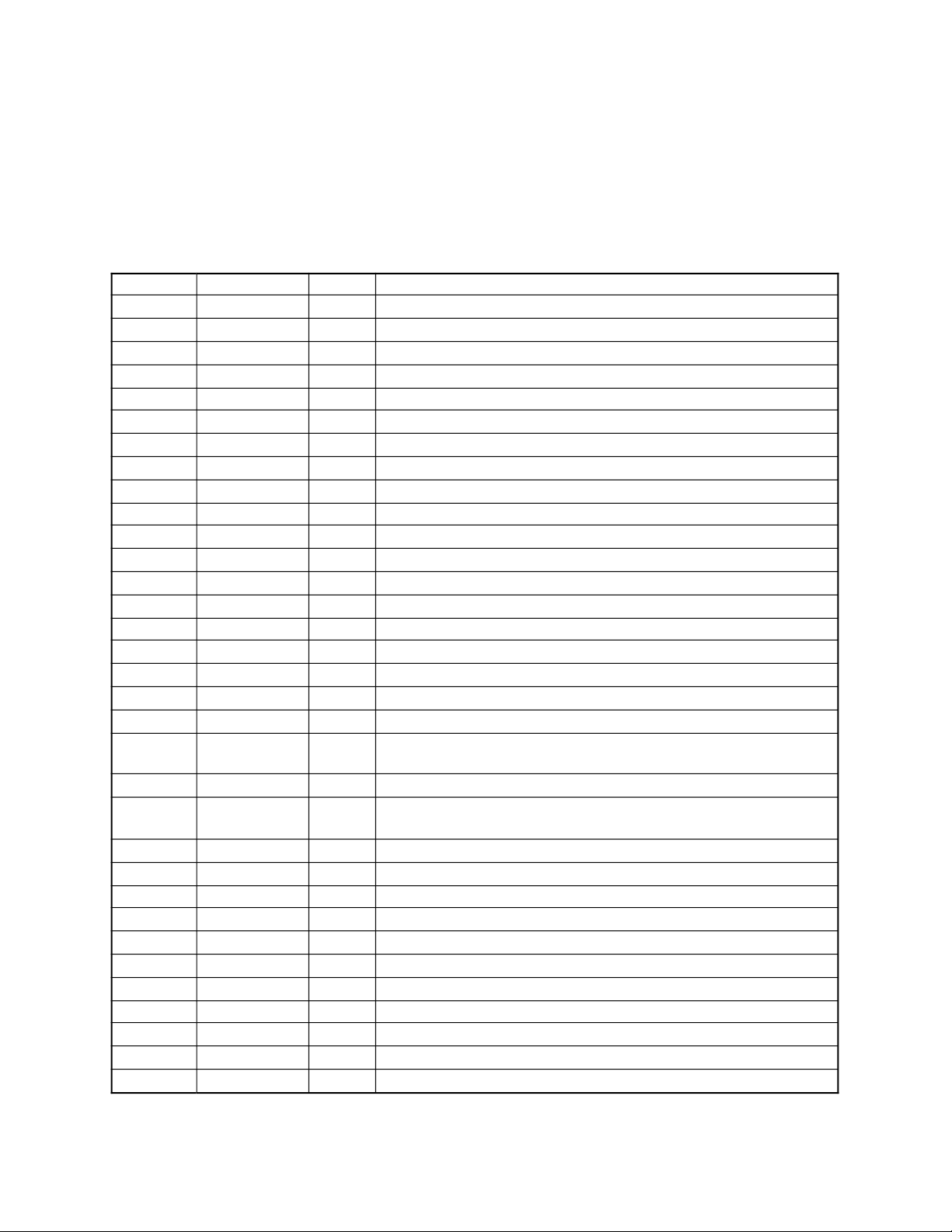
Specifications ................................................................................................................................2
Block Diagram............................................................................................................................... 3
Circuit Description ......................................................................................................................... 4
Major Waveforms ........................................................................................................................ 11
Printed Circuit Board ................................................................................................................... 12
Schematic Diagrams ................................................................................................................... 13
Exploded View ............................................................................................................................ 17
Parts List ..................................................................................................................................... 19
SPECIFICATIONS
GENERAL
Number of keys: 61
Polyphonic: 24-note (12 for some tones)
Preset tones: 100, with split/layer functions
Keyboard controls: Touch response: On/Off, Key transpose: 12 steps (F#-C-F)
Auto-rhythms: 100, Tempo control: 40 to 255
Auto-accompaniment: Mode: CASIO Chord/Fingered Chord/Full Range Chord
Controller: Intro/Fill-In, Synchro/Ending, Normal/Variation
Reverb effects: Hall/Stage/Room
Registrations: 6, Parameters registered: Tone No. (Normal, Layer, Split, Layer Split),
Rhythm No., Tempo, Accompaniment volume, Chord type, Reverberation
type, Split/Layer settings, Pitch bend range, Basic channel, Local on/off,
Portamento on/off
Song memory: 1, Real-time recording, Memory capacity: Approx. 1200 notes in total
Demo tunes: 1, including — Mei Wenti (Edward Alstrom)
Tuning control: 440Hz ± 50 cents
Built-in speakers: 12 cm dia. 2.5 W input rating: 2 pcs.
MIDI: 16 multi-channel reception
Terminals: Phone Jack [Output impedance: 110 Ω, Output voltage: 4.2 V(rms)
MAX], Sustain Jack, MIDI Jacks (IN, OUT), AC Adapter Jack (9 V) ,
Foot volume Jack
Auto power off: Approximately 6 minutes after the last operation
Power source: 2-way AC or DC source
AC: AC adapter
DC: 6 D size dry batteries
Power consumption: 7.7 W
Dimensions (HWD): 140 x 997 x 376 mm (5-1/2 x 39-5/16 x 14-13/16 inches)
Weight: 5.4 kg (11.9 lbs) without batteries
— 2 —
Page 3
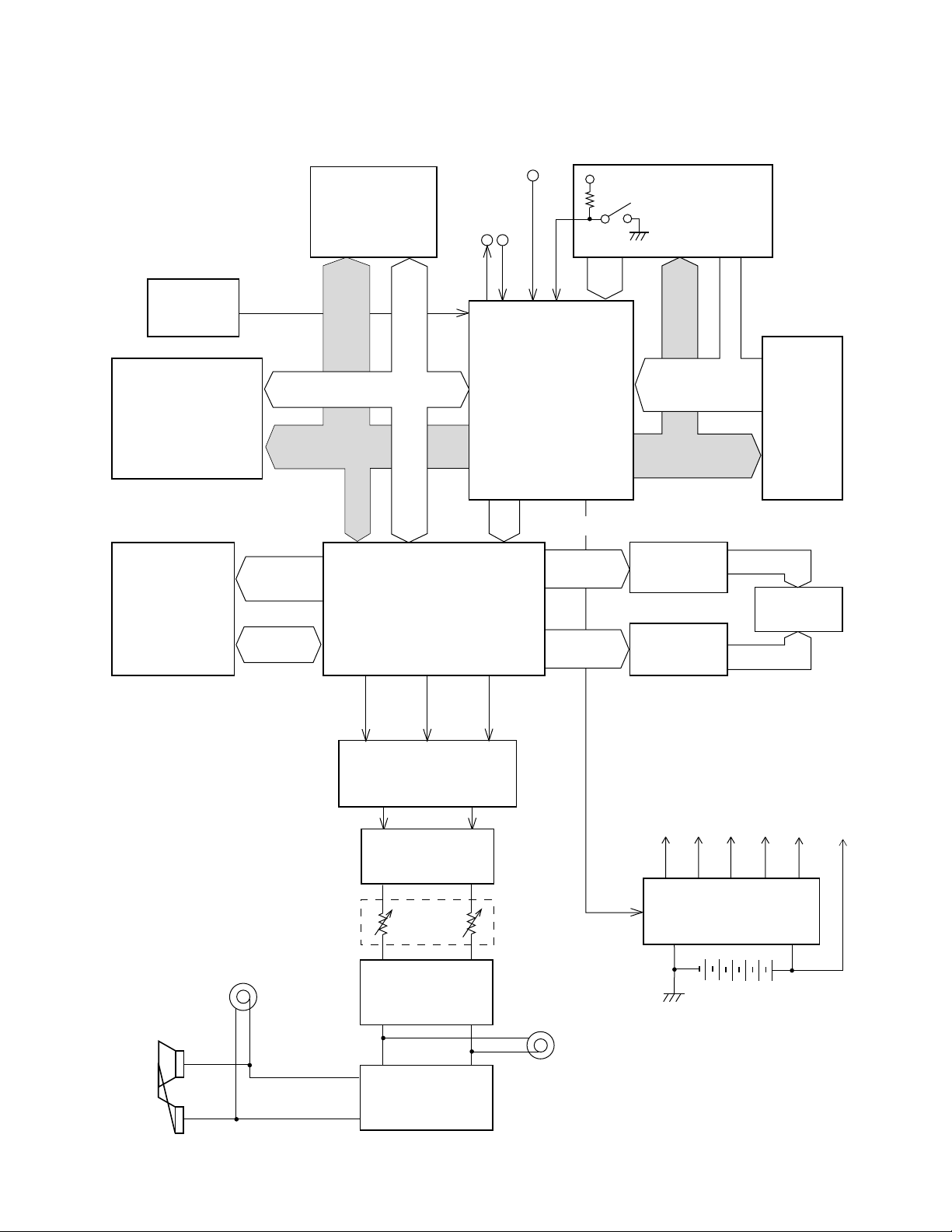
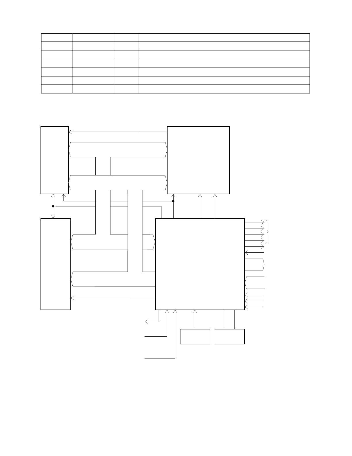
BLOCK DIAGRAM
Reset IC
IC106
RE5VA35AA
Sound Source ROM
(16M-bit)
LSI104
MX23C1610PC-
12CA38
Effect RAM
(64K-bit)
LSI105
LC3564S-10
RESET
MA0 ~ MA19
MA0, MA1
EA0 ~
EA12
EIO0 ~
EIO7
Working Storage
RAM (64K-bit)
LSI103
LC3564S-10
MA0
~
MA12
MD0 ~ MD15
MD0
~
MD7
HG51B277FB
DSP
LSI102
SUSTAIN
MIDI
INOUT
CPU
LSI101
UPD913GF-3BA
BCK, SO, LRCK
PA0 ~ PA6
PB0 ~ PB4
Power Switch
VDD
KI0 ~ KI2SI9
Buttons
FI0 ~ FI10
SI0 ~ SI8
KC0 ~ KC7
LED driver
Q401 ~ Q407
LED driver
IC105
BA612
FI9, FI10
Keyboard
La ~ Lg, Lh
LEDs /
7Seg. LED
LC0 ~ LC4
Speakers
Output
LRCK SO BCK
D/A Converter
IC106
UPD6379GR
Filter
Q115 ~ Q118
Main
Volume
Amp.
IC101
M5218APR
Power Amplifier
IC102
LA4598
Foot volume
APO
LVDD
VCC
AVDD
Power Supply Circuit
Q102 ~ Q109
D106, D108, D109
DVDD
VC
VDD
— 3 —
Page 4
CIRCUIT DESCRIPTION
KEY MATRIX
KC0 KC1 KC2 KC3 KC4 KC5 KC6 KC7
FI0 C2 (1) C#2 (1) D2 (1) D#2 (1) E2 (1) F2 (1) F#2 (1) G2 (1)
SI0 C2 (2) C#2 (2) D2 (2) D#2 (2) E2 (2) F2 (2) F#2 (2) G2 (2)
FI1 G#2 (1) A2 (1) A#2 (1) B2 (1) C3 (1) C#3 (1) D3 (1) D#3 (1)
SI1 G#2 (2) A2 (2) A#2 (2) B2 (2) C3 (2) C#3 (2) D3 (2) D#3 (2)
FI2 E3 (1) F3 (1) F#3 (1) G3 (1) G#3 (1) A3 (1) A#3 (1) B3 (1)
SI2 E3 (2) F3 (2) F#3 (2) G3 (2) G#3 (2) A3 (2) A#3 (2) B3 (2)
FI3 C4 (1) C#4 (1) D4 (1) D#4 (1) E4 (1) F4 (1) F#4 (1) G4 (1)
SI3 C4 (2) C#4 (2) D4 (2) D#4 (2) E4 (2) F4 (2) F#4 (2) G4 (2)
FI4 G#4 (1) A4 (1) A#4 (1) B4 (1) C5 (1) C#5 (1) D5 (1) D#5 (1)
SI4 G#4 (2) A4 (2) A#4 (2) B4 (2) C5 (2) C#5 (2) D5 (2) D#5 (2)
FI5 E5 (1) F5 (1) F#5 (1) G5 (1) G#5 (1) A5 (1) A#5 (1) B5 (1)
SI5 E5 (2) F5 (2) F#5 (2) G5 (2) G#5 (2) A5 (2) A#5 (2) B5 (2)
FI6 C6 (1) C#6 (1) D6 (1) D#6 (1) E6 (1) F6 (1) F#6 (1) G6 (1)
SI6 C6 (2) C#6 (2) D6 (2) D#6 (2) E6 (2) F6 (2) F#6 (2) G6 (2)
FI7 G#6 (1) A6 (1) A#6 (1) B6 (1) C7 (1)
SI7 G#6 (2) A6 (2) A#6 (2) B6 (2) C7 (2)
FI9
FI10
Intro/
Fill-In
Registration5Registration
Synchro/
Ending
6
Portament
Save
Start/
Stop
Normal/
Variation
Registration1Registration2Registration3Registration
4
Tempo
Up
Tempo
Down
Accomp.
Volume
Up
Accomp.
Volume
Down
KI0 Mode Rhythm 0 1 4 7 Layer Split
KI1 Reverb Tone – 2 5 8
Transpose
Tune/MIDI
KI2 +3 6 9
Song
Memory
Demo
Touch
Response
— 4 —
Page 5
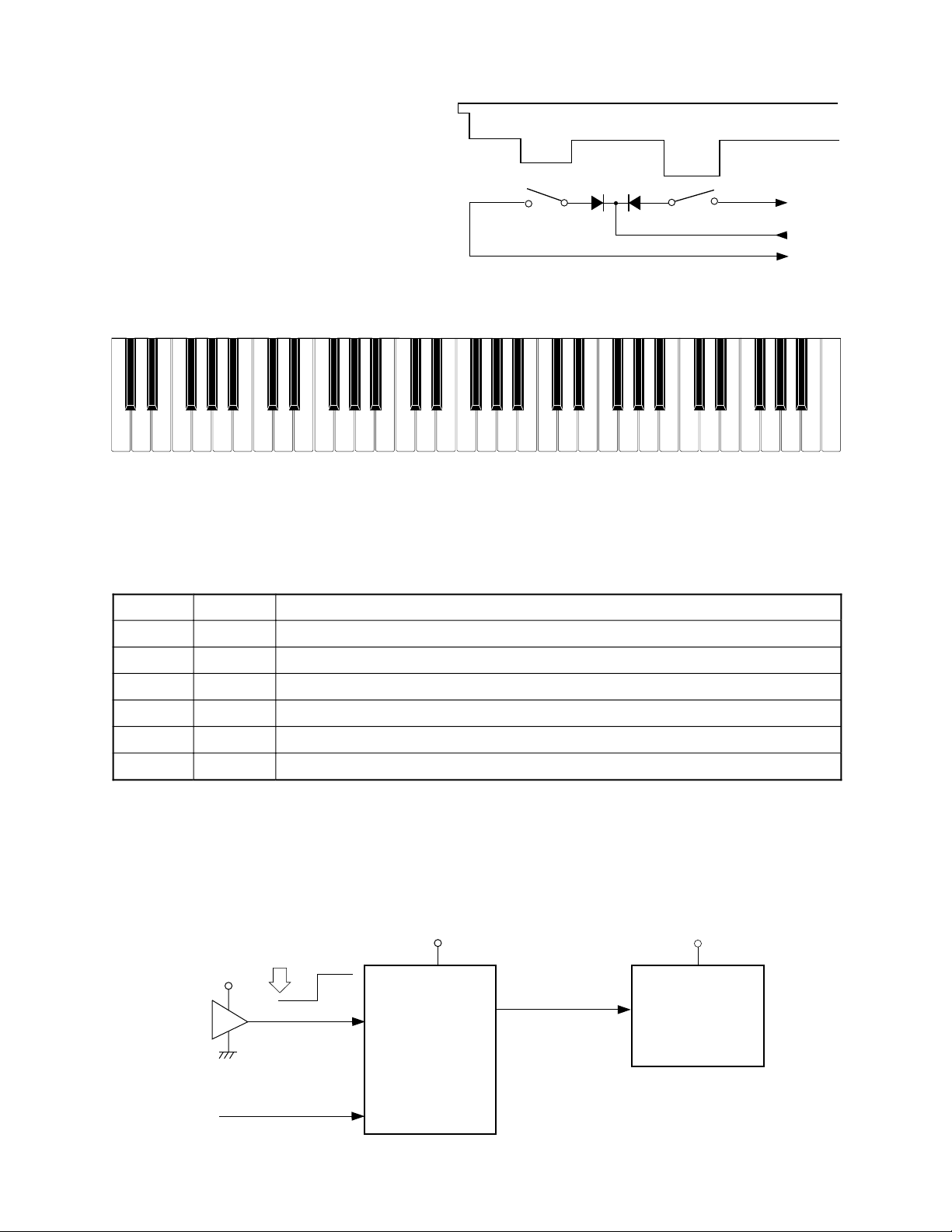
Note: Each key has two contacts,
the first conatct (1) and second contact (2).
NOMENCLATURE OF KEYS
Second contact (2)
Key
First contact (1)
FI
KC
SI
C#2
C2 D2E2F2G2A2 B2 C3 D3
F#2D#2
C#3A#2G#2
F#3 G#3
D#3
E3
F3 G3 A3 B3 C4 D4 E4 F4 G4 A4 B4 C5 D5 E5 F5 G5 A5 B5
A#3 C#4 D#4
F#4 G#4
A#4
C#5
D#5
F#5 G#5
A#5
C#6
C6
G#6F#6D#6
A#6
POWER SUPPLY CIRCUIT
The power supply circuit generates six voltages as shown in the following table. VDD voltage is always
generated. The others are controlled by APO signal from the CPU.
Name Voltage For operation of
VDD +5 V CPU, Reset IC, DSP, Sound source ROM, Working storage RAM, Effect RAM
DVDD +5 V Power jack, Sustain jack, MIDI jack
AVDD +5 V DAC, Filter
LVDD +5 V LED Driver
VCC +9 V Power amplifier, Pilot lamp
VC +9 V Power amplifier
B6A6G6F6E6D6
C7
RESET CIRCUIT
When batteries are set or an AC adapter is connected, the reset IC provides a low pulse to the CPU. The
CPU then initializes its internal circuit, and clears the working storage RAM.
When the power switch is pressed, the CPU receives a low pulse of POWER signal, then the CPU sends
a reset signal to the DSP.
Battery set
VDD
Reset IC
IC106
RE5VA35AA
POWER
From power switch
RESET
VDD
CPU
LSI101
UPD913GF-3BA
NMI
— 5 —
Reset signal
PLE
HG51B227FB
VDD
DSP
LSI102
Page 6
CPU (LSI101: UPD913GF-3BA)
The 16-bit CPU contains a 1k-byte RAM, three 8-bit I/O ports, two timers, a keycontroller and serial interfaces.
The CPU detects key velocity by counting the time between first-key input signal FI and second-key SI from
the keyboard. The CPU reads sound data and velocity data from the sound source ROM in accordance with
the selected tone; the CPU can read rhythm data simultaneously when a rhythm pattern is selected. Then the
CPU provides 16-bit serial sound data to the DSP. The CPU also controls MIDI input/output and stores
sequencer data into the working storage RAM.
The following table shows the pin functions of LSI101.
Pin No. Terminal In/Out Function
1 TXD0 Out MIDI signal output
2 RXD0 In MIDI signal input
3 SCK0 Out APO (Auto Power Off) signal output
4, 5 TXD1, RXD2 — Not used. Connected to ground.
6 SCK1 Out 1 MHz synchronizing pulse output
7 AVCC In +5 V source
8 AN0 In Pitch bend control voltage input
9 AN1 In Modulation control voltage input
10 AGND In Ground (0 V) source
11 BCK Out Bit clock output
12 SO Out Serial sound data output
13 LRCK Out Word clock output
14 GND In Ground (0 V) source
15, 16 XLT0, XLT1 In/Out 20 MHz clock input/output
17 VCC In +5 V source
18, 19 MD0, MD1 In Mode selection terminal
20 RSTB In Reset signal input
21 NMI In Power ON signal input
22 INT — Not used. Connected to ground.
23 ~ 30
31 ~ 38 KC0 ~ KC7 Out Terminal for key input signal
39 ~ 46
47, 48 FI8, SI8 — Not used
49 FI9 In Terminal for button input signal
50 SI9 In Substain signal input
51 FI10 In Terminal for button input signal
52 SI10 In Not used
53 ~ 55 KI0 ~ KI2 In Terminal for button input signal
56 MWNB Out Write enable signal output
57 ~ 76 MA0 ~ MA17 Out Address bus
77 MCSB0 Out Chip enable signal output for the sound source ROM
78 MCSB1 Out Not used
79 MCSB2 Out Chip enable signal output for the DSP
FI0 ~ FI3
SI0 ~ SI3
FI4 ~ FI7
SI4 ~ SI7
In Terminal for key input signal
In Terminal for key input signal
— 6 —
Page 7
Pin No. Terminal In/Out Function
80 VCC In +5 V source
81 GND In Ground (0 V) source
82 MRDB Out Read enable signal output
83 ~ 98 MD0 ~ MD15 In/Out Data bus
99 PLE Out Reset signal output for the DSP
100 P17 In APO cancellation signal input
CPU Block Diagram
CE
RAM
LSI103
OE
OE
ROM
LSI104
WE
MWEB
MRDB
CE
MD0 ~ MD7
MA0 ~ MA10
MD0 ~ MD15
MA0 ~ MA19
MCSB0
MA0/MA1
RCEB
MRDB
SCK0
P17
WEB
MWNB
NMI
DSP
LSI102
CE1B
MCSB2
CPU
LSI101
RSTB
RESB
PLE
TXDO
RXDO
SCK1
BCK
SO
LRCK
SI9
AN1
AN0
XLT0/XLT1
Sound data and
timing signals
MIDI input/output
KC0 ~ KC7
FI0 ~ FI10, SI0 ~ SI7
KI0 ~ KI2
Sustain signal
Modulation
Pitch bend
APO
APO cancel signal
Power ON signal
Reset IC PG 20MHz
— 7 —
Page 8

DIGITAL SIGNAL PROCESSOR (LSI102: HG51B277FB)
The DSP receives 16-bit serial sound data output from the CPU and adds the selected effect to the sound
data using the effect RAM. Then the DSP provides the sound data to the DAC. The DSP contains two I/O
ports, which controls LEDs.
The following table shows the pin functions of LSI102.
Pin No. Terminal In/Out Function
1 ~ 4, 80 PB0 ~ PB4 Out LED drive signal output
5 SO Out Serial sound data output for the DAC
6 WCKO Out Word clock output for the DAC
7 VDD3 In +5 V source
8 TEST — Not used.
9 RESB In Reset signal input
10 VSS2 In Ground (0 V) source
11, 12 XIN, XOUT In/Out 16 MHz clock input/output
13 WCKI In Word clock input from the CPU
14 SI In Serial sound data input from the CPU
15 BCKI In Bit clock input from the CPU
16 SINC In 1 MHz synchronizing pulse input
17 VDD2 In +5 V source
18 ~ 25 IO0 ~ IO7 In/Out Data bus
26 RCEB Out Chip enable signal output for the working storage RAM
27 VSS3 In Ground (0 V) source
28 AD1 In Address bus
29 OEB In Not used. Connected to +5 V source.
30 WEB In Write enable signal input
31 VDD3 In +5 V source
32 CE2 In Chip enable signal input. High active.
33 AD0 In Address bus
34 CE1B In Chip enable signal input. Low active.
35 ~ 41, 43 EIO0 ~ EIO7 In/Out Data bus for the effect RAM
42, 44, 46 ~
48, 51 ~ 57, 59
45 ECEB Out Chip enable signal output for the effect RAM
49 EOEB Out Read enable signal output for the effect RAM
50 VSS3 In Ground (0 V) source
58 EA13 Out Not used
60 EWEB Out Write enable signal output for the effect RAM
61 EA14 Out Not used
62, 66, 70, 74,
78
63, 67, 71, 75,
79
64, 65, 68, 69,
72, 73, 76, 77
EA0 ~ EA12 Out Address bus for the effect RAM
VSS2 In Ground source
VDD2 In +5 V source
PA0 ~ PA7 Out LED segment signal output
— 8 —
Page 9

DSP Block Diagram
Effect RAM Access
APO
CE2
CE1
WE
OE
ECEB
EWEB
EOEB
RAM
LSI105
EI00 ~ EI07
EA0 ~ EA12 PB0 ~ PB4
DAC (LSI106: UPD6379GR)
LED Driving
LVDD
Q401 ~ Q407
Q120
PA0 ~ PA7
La ~ Lh
DSP
LSI102
IC105
LC0 ~ LC4
LG
The DAC receives 16-bit serial data output from the DSP. The data contains digital sound data of the
melody, chord, bass, and percussion for the right and left channels. The DAC converts the data into
analog waveforms and output them to each channel separately.
Synch signal
L OUT
R OUT
DAC
LSI106
UPD6379GR
SI
Word clock
LRCK
CLK
Data
WCKO
Bit clock
SO
DSP
LSI102
HG51B277FB
SINC
SI
Word clock
WCKI
Bit clock
BCKI
Data
SCK1
SO
LRCK
BCK
CPU
LSI101
UPD913GF-3BA
— 9 —
Page 10

FILTER BLOCK
Since the sound signals from the DAC are stepped waveforms, the filter block is added to smooth the
waveforms.
AVDD
AVDD
To main volume
10V22µ
2SC1740SQ
2.2 K
C331
1 K
C332
2SC1740SQ
1 K 1 K
C331
1 K
AG
18 K
50 V 0.22 µ
47 K
AG
From the DAC
AG
AG
AG
POWER AMPLIFIER (IC102: LA4598)
The power amplifier is a two-channel amplifier with standby switch.
The following table shows the pin function of IC101.
Pin No. Terminal In/Out Function
1 Power GND In Ground (0 V) source
2 Ch1 B.S. — Terminal for a bootstrap capacitor
3 Ch1 OUT Out Channel 1 output
4 VCC In +9 V source
5 Ch1 N.F. In Negative feedback input
6 Ch1 IN In Channel 1 input
7 D.C. — Terminal for a decoupling capacitor
8 Pre GND In Ground (0 V) source
9 Stand by In Power control signal input. 0 V: Off, +9 V: On
10 Ch2 IN In Channel 2 input
11 Ch2 N.F. In Negative feedback input
12 Ch2 OUT Out Channel 2 output
13 Ch2 B.S. — Terminal for a bootstrap capacitor
14 NC — Not used
— 10 —
Page 11

MAJOR WAVEFORMS
1
2
3
CH1: CH2:
5 V5 V
1 POWER ON signal
UPD913GF-3BA pin 21
2 APO signal
UPD913GF-3BA pin 3
3 Reset signal for the DSP
UPD913G-3BA pin 99
0.1 s
CH1
CH2
4
5 VCH1:
4 Synchronizing pulse
UPD913GF-3BA pin 6
20 µs
CH1
A
B
C
5 VCH1: 5 VCH2: 5 VCH3:
A Word clock LRCK
UPD913GF-3BA pin 13
B Data signal SO
UPD913GF-3BA pin 12
C Bit clock BCK
UPD913GF-3BA pin 11
2 µs
D
CH1
E
CH2
F
CH3
Note: On
2 µs
CH1
CH2
CH3
5 VCH1: 5 VCH2: 5 VCH3:
D Word clock LRCK
UPD6379GR pin 1
E Data signal SI
UPD6379GR pin 2
F Bit clock CLK
UPD6379GR pin 3
5
6
7
5 VCH1: 5 VCH2: 5 VCH3:
5 Key scan signal KC0
UPD913GF-3BA pin 31
6 Key scan signal KC1
UPD913GF-3BA pin 32
7 Key scan signal KC2
UPD913GF-3BA pin 33
50 µs
CH1
CH2
CH3
8
9
0
5 VCH1: 5 VCH2: 5 VCH3:
8 LED drive signal PB0
HG51B227FB pin 80
9 LED drive signal PB1
HG51B227B pin 1
0 LED drive signal PB2
HG51B227FB pin 2
5 ms
CH1
CH2
CH3
G
H
CH1: . 1 V
~
CH2: . 1 V
G DAC output (R-ch)
UPD6379GR pin 5
H DAC output (L-ch)
UPD6379GR pin 8
1 ms
CH1
1 ms
CH1
I
CH2
CH2
J
~
CH1: 0.5 V
~
CH2: 0.5 V
~
I Pre-amp. output (R-ch)
M5218APR pin 7
J Pre-amp. output (L-ch)
M5218APR pin 1
Tone : Whistle (68)
Key : A4
Touch response : Off
Reverb : Off
Volume : Maximum
— 11 —
Page 12

Main PCB JCM469-MA1M
PRINTED CIRCUIT BOARD
16
1920
1112134231718
8
9
10
15
14
— 12 —
1567
Page 13

Main PCB JCM469-MA1M/MA2M
SCHEMATIC DIAGRAMS
18
20
19
17
8 9 10
3
2
4
14 15 16
11 12 13
1
Note:
1. All capacitance values are indicated in "µF"
(p=10-6 µF).
2. All resistance values are indicated in "Ω"
(k=103 Ω, M=106 Ω).
5 6 7
— 13 —
Page 14

Console PCB JCM469-CN1M
— 14 —
Page 15

Controller PCBs JCM469-CN2/CN3
— 15 —
Page 16

Keyboard PCBs JCM617T-KY1M/KY2M
— 16 —
Page 17

16
7
8
9
9
6
10
13
14
12
11
14
15
R-1
2
1
24
10
23
3
4
5
22
19
17
18
R-2
20
21
R-3
EXPLODED VIEW
— 17 —
Page 18

PARTS LIST
CT-870
Notes: This parts list does not include the cosmetic parts, which
parts are marked with item No. "R-X" in the exploded
view.
Contact our spare parts department if you need these
parts for refurbish.
1. Prices and specifications are subject to change without prior notice.
2. As for spare parts order and supply, refer to the
"GUIDEBOOK for Spare parts Supply", published
seperately.
3. The numbers in item column correspond to the same
numbers in drawing.
Page 19

Item Code No. Parts Name Specification Q R
Main PCB
1 6925 4800 Main PCB ass'y M469-MA1.2M M140392*1 1 B
LSI101 2012 3668 LSI, CPU UPD913GF-3BA 1 A
LSI102 2012 0441 LSI, DSP HG51B277FB 1 A
LSI103/105 2012 0700 LSI, RAM LC3564S-10 2 A
LSI104 2012 3661 LSI, ROM MX23C1610PC-12C38 1 A
LSI106 2105 4249 LSI, DAC UPD6379GR 1 A
IC101 2114 1799 IC M5218APR 1 A
IC102 2114 2891 IC LA4598 1 A
IC104 2114 1421 IC PC900V 1 A
IC105 2114 3318 IC BA612 1 A
IC106 2105 3941 IC RE5VL35AA-TZ
Q101, Q106, 2200 4409 Transistor 2SA933SQ-TP-T
Q120
Q102/104 2251 0469 Transistor 2SB1237Q,R-TV6-T 2 A
2220 1387 Transistor 2SC1740SQ-TP-T 10 A
Q108 2253 0357 Transistor 2SD2008Q,R-T105-T
Q111/112 2253 0420 Transistor 2SD1468SR,S-TP-T 2 A
D101/111
D102 2390 0371 Diode DSK10B-BT-T 1 B
D106, D108
D109, D112/113 2360 1646 Zener diode MTZJ5.6CT-77-T 3 B
D116 2360 2079
X101 2590 0203 Ceramic oscillator CSA16.00MX040 1 B
X102 2590 2009 Crystal oscillator HC-49/US20A
J101 3501 7049 Jack HEC2305-01-330
J102 3612 0665 Jack YKB21-5006
J103 3613 0938 Jack HLJ4416-01-3040
J104 3612 0789 Jack YKB21-5010
J105 3501 4816 Jack YKF51-5051 1 B
VR101
2 6925 4810 Console PCB ass'y M469-CN1M M140393*1 1 B
Q401 - Q407 2200 4409 Transistor 2SA933SQ-TP-T 7 B
LED401 2370 1141 LED SL-9352-60 1 B
LED409/410 2370 1190 LED MVR3378S 2 C
3 6925 4820 Controller PCB ass'y M469-CN2.3 M240412*1 1 B
4 6923 6940 PCB ass'y M617T-KY1M M140211*1 1
D501 - D564 2301 0101 Diode 1S2473-T-77-T
5 6923 6950 PCB ass'y M617T-KY2M M140212*1 1
D565 - D622 2301 0101 Diode 1S2473-T-77-T
6 6906 8291 Rubber button M312088-5
7 6922 2680 Rubber button M312082-2
8 6925 4960
9 6923 4980 Rubber button M312122-2
10 6923 4990 Rubber button M312123-2
Notes: Q – Used quantity
2390 1323 Diode RB100A-T32-T
2390 1344
2360 1085 Zener diode HZS6B1LTD-T
2765 1575 Volume EWA-MJ0S10B23
Console PCB
2390 1344 Diode 1SS133T-77-T 37 B
2370 0616 LED LN28RPX-(TT2) 11 C
Controller PCBs
2370 0616 LED LN28RPX-(TT2) 1 C
3502 2180 Stick controller RKJXK1220-9-50K 1 A
Keyboard PCBs
Mechanical Parts
R – Rank
Diode
Zener diode
Rubber button
1SS133T-77-T 6 B
MTZJ4.7AT-77-T 1 B
M312082-4
1
3
1
2
2
1B
1B
1B
1B
1B
1
64
58
1B
1
1
2
3
A
A
A
B
B
A
B
C
B
C
B
B
B
B
— 19 —
Page 20

Item Code No. Parts Name Specification Q R
11 6925 4970 Rubber button M312125-4 1
12 6925 4980 Rubber button M240099-2
13 6925 4990
14 3831 0413 Speaker KC120FEL
15 6921 5040
16 6925 4920 Display plate M340457-1
17 6922 2860 White key set, CS M340503*2 1
18 6922 2850 White key set, CB M340503*1
19 6922 2750 Black key set, 5-key M111726-2
20 6922 2740 Black key set, 10-key M111726-1
21 6922 2760 Key contact rubber M211704-1
22 6922 2770 Key contact rubber M211705-1
23 6925 2570 Control stick M340475-1
24 6918 1630 Battery cover M311164*1
Accessories
1014 9396 AC adapter (for China only) AD-5CL-SC1(D)
6925 4890 Console sheet (for China only) M140380-1
Rubber button
Slide knob
M240403-1
M311860-1
B
B
1
B
1
B
2
B
1
C
1
A
A
4
A
1
A
2
A
4
A
1
A
1
B
1
1B
1B
Notes: Q – Used quantity
R – Rank
— 20 —
Page 21

MA0900361A
Sep, 1996
 Loading...