


Part 2
Technical
Information
1. TECHNICAL DESCRIPTION
1.1 AF System
While based on the EOS-3, the EOS-1V’s AF system incorporates major enhancements including a newly designed AF unit and a new AI Servo AF sequence and
algorithm for improved speed, precision, and reliability. Other components are
based on the EOS-3’s such as the large, oval secondary mirror, the optical system’s basic configuration and focusing principle, the focusing point’s automatic
selection algorithm, and the low-contrast countermeasures.
1) Faster Area AF
● High-speed, 33.3 MHz, RISC microcomputer and high-speed software processing
The high-speed RISC microcomputer
with a clock speed of 33.3 MHz is dedicated to AF calculations and shooting
data memory. The processing speed is
faster than the EOS-3’s (clock speed:
24.576 MHz). And with the same highspeed, predictive calculation algorithm
and other software processing, the
focusing point selection speed is faster than the EOS-3’s. Even the manual focusing point selection speed is the world’s fastest.
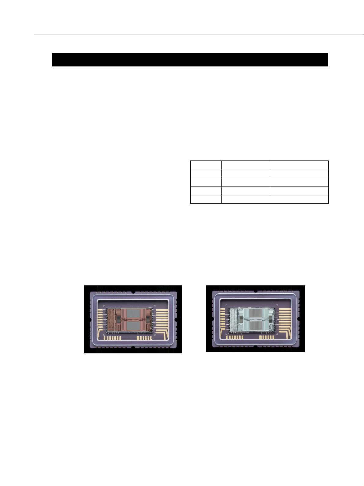
2) Area AF with higher precision
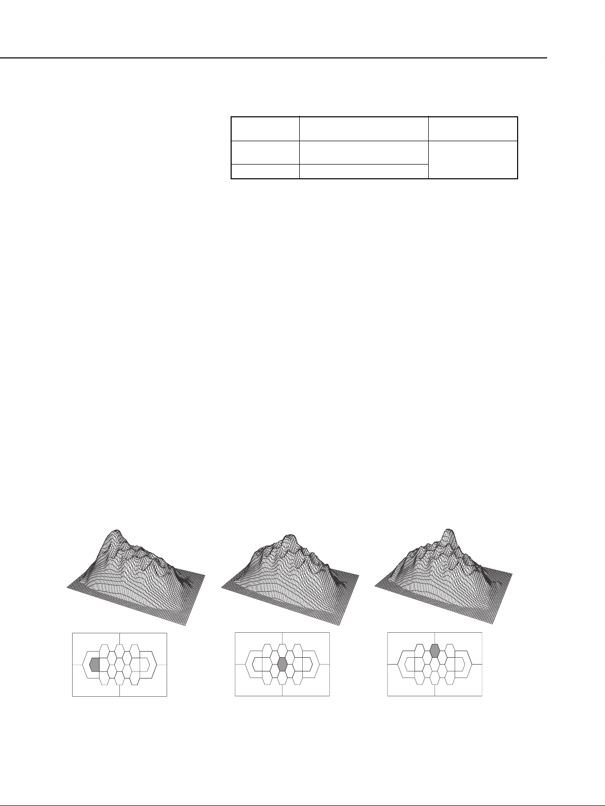
● Improved S/N ratio and in-focus indicator with guaranteed precision
q To further improve the S/N ratio, the sensor’s effective light-sensing area per
pixel has been increased by 12 percent. Also, the AF sensor’s light-sensing surface has an anti-reflection layer to reduce the ghosting that affects the S/N ratio.
(Fig. 2-1)
w In low-light, whether focus has been achieved or not depends on how reliable the
focusing signal is. To obtain the correct result, focusing signal precision has been
given priority. Of course, focusing precision is officially guaranteed in low light
down to EV 0.*
* Although this specification is common to all EOS cameras, it has not been men-
tioned in the manual until now.
2-1
Part 2: Technical Information
Camera
EOS-1
EOS-1N
EOS-3
EOS-1V
Basic Clock Speed
12 MHz
12 MHz
24.576 MHz
33.3 MHz
Fastest Processing Speed
0.33 µs
0.17 µs
0.04 µs
0.03 µs
Table 2-1 AFCPU
Fig. 2-1 EOS-1V’s AF sensor. Fig. 2-2 EOS-3’s AF sensor.
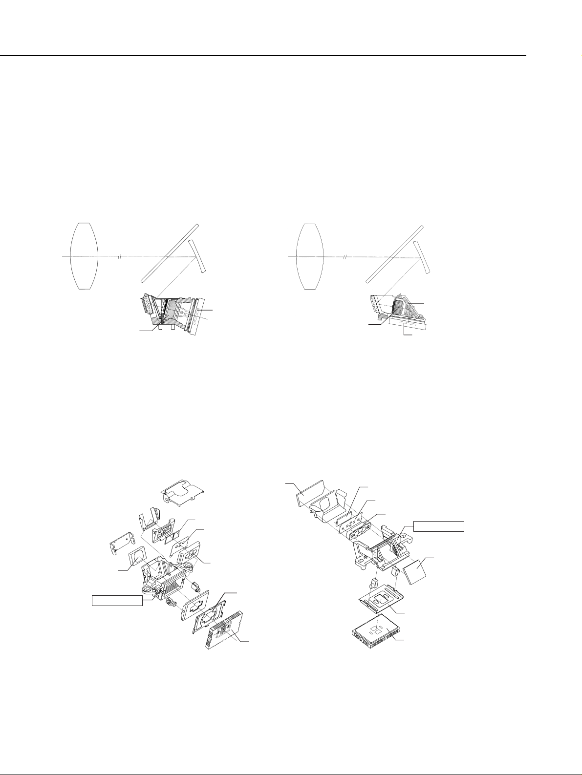
3) Area AF with higher reliability
● New AF optical system eliminating unstable precision
The new AF optical system (Fig. 2-3) does not have the fully-reflective mirror 2
which the EOS-3 has near the sensor. The mirror’s reflective surface which
caused unstable precision has thereby been eliminated.
Also, the secondary image-forming lens is now made of molded glass instead of
plastic resin. It enables consistent focusing precision even under high temperatures and humidity.
● AF unit in a strong box
The AF unit’s AF chassis (Fig. 2-4) is now made of a material whose properties
change little when the humidity changes. The rigid box construction is also able
to withstand shock and other environmental influences to improve precision stability.
2-2
Part 2: Technical Information
Prime lens
Main reflex mirror
Secondary mirror
Prime lens
Main reflex mirror
Secondary mirror
Fully-reflective mirror Fully-reflective mirror 1
Fully-reflective
mirror 2
Secondary
image-forming lens
Area AF sensor
Area AF sensor
Secondary
image-forming lens
EOS-1V AF optical system EOS-3 AF optical system
Fig. 2-3 Comparison of the EOS-1V and EOS-3’s AF optical systems.
Fully-reflective
mirror 1
Fully-reflective
mirror 2
Infrared filter
Fixed diaphragm
Secondary image-forming lens
Center holder
Area AF sensor
Fully-reflective
mirror
AF chassis
Infrared filter
Fixed diaphragm
Secondary image-forming lens
Center holder
Area AF sensor
EOS-1V AF unit EOS-3 AF unit
AF chassis
Fig. 2-4 Comparison of EOS-1V and EOS-3’s AF units.
4) Predictive AI Servo AF Control
During continuous shooting, the EOS-3’s AI Servo AF incorporates shutter release
priority for the first shot and focusing priority (lens drive priority) from the second
shot onward. So for a fast-moving subject at a close distance, the first shot might
be out of focus (the point of focus is in front of the subject) or camera shake may
cause focusing error. This causes the continuous film advance speed to become
irregular.
To resolve this problem with the EOS-1V, the priority control for the first shot
during AI Servo AF continuous shooting has been changed and the predictive AF
algorithm and continuous shooting sequence for 9 fps have been newly developed.
The result is better focus tracking of the subject and better focusing precision.
The continuous film advance speed is also more stable.
(1) AI Servo AF control for the first shot
The EOS-3’s predictive AF control (Fig. 2-
5) stops driving the lens immediately
when the shutter is released. Therefore,
for a subject moving quickly across the
image plane, the camera must overshoot
the predictive lens drive amount to compensate for the time lag between the lens
drive stoppage and the start of the exposure. Depending on the moment of the
shutter release, the lens drive overshoot
might be excessive, resulting in the point
of focus falling slightly in front of the subject. Since a point of focus in front of the
subject is more favorable (the picture is
still salvageable) than one behind the subject, this control inclination was intentional.
● The lens, aperture, and mirror are driven
simultaneously from the first shot with the
EOS-1V.
When focus must be achieved as quickly
as possible during AF search, the standard power is used after focus is achieved
during AI Servo AF when the lens drive
amount for the maximum power and time is minimal. This enables the predictive
lens drive, aperture, and reflex mirror to be driven simultaneously (with or without PB-E2 attached). It reduces the lens drive overshoot amount before the shutter is released.
* AF search drive: During SW-1 ON when the AF system cannot detect the sub-
ject, the lens is driven to find the subject.
* AI Servo AF drive: After focus is achieved, the moving subject is tracked during
continuous focusing.
* Standard power: This is the amount of power supplied to the lens at the EOS-
1N’s level.
* Maximum power: This is twice the amount of the standard power.
2-3
Part 2: Technical Information
Shutter released
EOS-3
Lens drive stops
Aperture stopped down
Mirror goes up
Exposure
Shutter released
AI Servo AF
Lens driven
AI Servo AF
Lens driven
EOS-1V
Aperture stopped down
Predictive lens drive
Mirror goes up
Lens drive stops
Exposure
AF search
Lens driven
AF search
Lens driven
Maximum
power supplied.
Power cut
by half.
Power stopped.
Power supply to lens drive
Fig. 2-5 Comparison of
AI Servo AFcontrol.
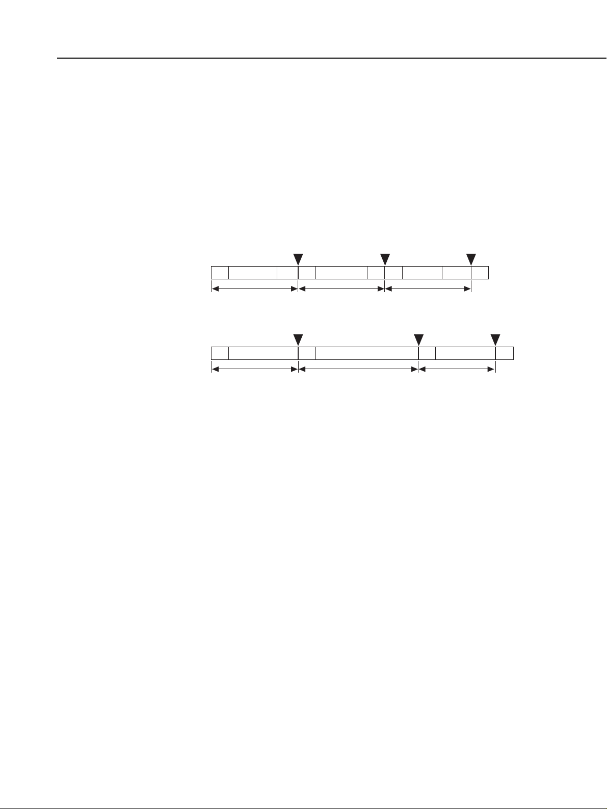
● Lens driving time setting after SW-2 ON
Regardless of when the shutter is released, the lens drive stops at the predicted
point of focus. The lens driving time after SW-2 ON is set (0 - 35 ms). Thus, while
shutter release-priority is maintained, the correct focus drive is obtained for the
predicted point of focus.
(2) AI Servo AF control from the second shot onward
To improve the EOS-1V’s AI Servo AF tracking perfor mance and focusing precision and to maintain the film advance speed at a consistent level, the following
measures were incorporated. Other than the below, the basic AI Servo AF control
system is the same as the EOS-3’s.
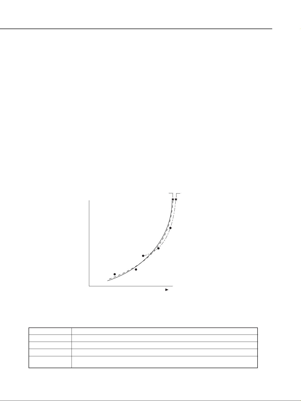
q New predictive AF algorithm suited for 9 fps
● High-precision, predictive AF with statistical operation and analysis
The EOS-3 refers to the last three focusing data readings to predict the next point
of focus. However, the EOS-1V uses more focusing data for statistical operation
and analysis (Fig. 2-6) and compensates for focusing error while predicting the
point of focus. This increases the probability of obtaining the correct focus in the
AI Servo AF mode. And since this enables a stable lens drive and a correct predictive point of focus, it is more likely for the lens drive to end within the time alloted
during the maximum-speed sequence of 9 fps. This also helps to stabilize the
continuous shooting speed. Table 2-2 shows the process of predicting the point of
focus from the first to fourth focusing attempts and beyond.
2-4
Part 2: Technical Information
, Focusing error
Far
Movement speed on image plane
Low speed
High speed
Near
Subject distance
Predictive point of focus
with other cameras
Statistical operation and
predictive point of focus
Subject movement condition/
Fig. 2-6 Comparison of statistical operation and conventional predictive operation.
Focusing Attempts
First time
Second time
Third time
Fourth time onward
Predictive Focusing Method
The lens drive amount from the point of defocus to the point of focus is detected.
With the first focusing data reading, the next point of focus is predicted.
With the first and second focusing data readings, the next point of focus is predicted.
The focusing data obtained so far is used for statistical operation and the focusing error is
corrected to obtain a more precise predicted point of focus.
Table 2-2 Point of Focus Prediction Process
w New continuous shooting sequence
With the EOS-3, the shutter releases immediately when the lens driving ends.
This causes an irregular lens driving time which in turn makes the film
advance speed irregular as well. Since the focusing time for each shot is also
irregular, predictive focusing control also becomes more difficult.
● Exposure standby until the set time after the lens drive ends
During the 9 fps continuous shooting sequence, the exposure is delayed until the
set standby time elapses (since the lens is being driven forward during this standby time, the focus is not affected) even if the lens drive ends earlier (Fig. 2-7). The
standby time cushions the irregular lens driving time, and it thereby stabilizes
the continuous shooting speed increases the probability for achieving correct
focus.
● Securing the exposure standby time
The shooting speed is set to 9 fps even when AI Servo AF can exceed 9 fps. The
extra time is used to stabilize the continuous shooting speed. The ultra-high
speed shooting sequence at 10 fps in the One-Shot AF mode and the new predictive AF algorithm and high-speed EF lenses make it possible to set a standby
time. In the high-speed continuous shooting mode at 7 fps, the sequence provides
even more extra time. Continuous shooting in the AI Servo AF mode is therefore
more stable than with the EOS-3.
● Continuous shooting speed adjusted to suit the lens driving time
If the lens driving cannot be completed within the set time due to difficult subject
tracking conditions, the film advance speed is decreased (in 0.5 fps increments) to
a stable level that is maintainable. This is to prevent the film advance speed from
becoming irregular. When the subject tracking becomes easier, the film advance
speed is increased again.
2-5
Part 2: Technical Information
Standby
AF AF
Lens driven
Exposure starts
Standby
AF
Lens driven
Standby
AF
Lens driven
Exposure starts Exposure starts
AF AF
Lens driven
Exposure starts
AF
Lens driven
AF
Lens driven
Exposure starts Exposure starts
The standby time absorbs the irregular lens driving time, and the AF interval
and exposure interval become uniform.
With no standby time, the irregular lens driving time directly affects the AF interval
and exposure interval.
Standby time provided
No standby time
Fig. 2-7 Comparison of continuous shooting sequences.

(3) Preconditions for attaining 9 fps
When the PB-E2 + NP-E2 and an EF lens having the EF 300mm f/2.8L IS USM’s
lens drive speed are attached to the camera and the lens EMD stopdown time is
35 ms or shorter (equivalent to 2 stops worth with the EF 300mm f/2.8L IS
USM), 9 fps is attained when the lens drive ends within the time in the maximum-speed sequence described above.
The EMD stopdown time decreases the continuous shooting speed accordingly.
Also, when the focusing point selection is automatic during predictive AF and the
subject moves to another focusing point, the continuous shooting speed and the
predictive AF perfor mance deteriorate slightly (by how much depends on how
often the subject moves to another focusing point) due to the extra focusing and
processing time required. The deterioration occurs even while the PB-E2 is
attached to the camera.
e Predictive AF control perfor mance
● 50 kph at 8 meters
The camera can focus track a subject approaching the camera at 50 kph up to 8
meters away (with the EF 300mm f/2.8L IS USM). Each of the 45 focusing points
is capable of the same predictive AF perfor mance. As mentioned before, AI Servo
AF control for the first shot is the same with or without the PB-E2 attached.
Therefore, the predictive AF perfor mance with the EOS-1V is the same with or
without the PB-E2 attached.
When the battery becomes exhausted, the lens, aperture, and reflex mirror are
driven sequentially instead of simultaneously, resulting in lower perfor mance of
the predictive AF control.
2-6
Part 2: Technical Information
100
[m]
Subject Distance
10
1
5 10 50 100 500
Subject Movement Speed (kmh)
EOS-1N
+ PDB-E1: 5 fps
EOS-1V: 9 fps
EOS-3: 7 fps
Fig. 2-8 Comparison of predictive AF control performance.
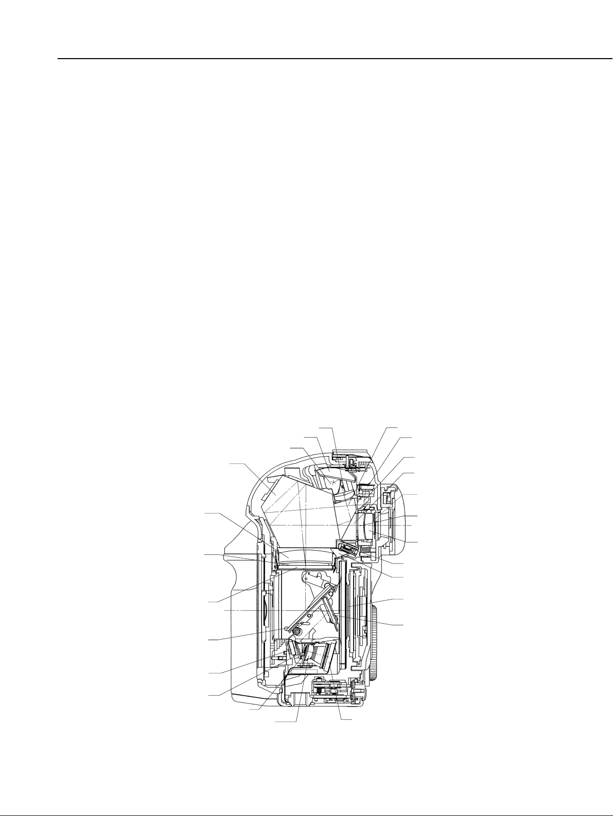
1.2 Viewfinder
1) Configuration
The viewfinder’s basic optical system is the same as the EOS-3’s. The coverage is
100%, the viewfinder magnification is 0.72 ×, dioptric correction is provided, an
eyepiece shutter is provided, and superimposition (SI) display optics is provided.
Even without the Eye Control unit, there was a problem with too little space. The
basic configuration was revamped to minimize space requirements, and the SI
display brightness was increased.
The major changes in the configuration are as follows:
● Pentaprism with a high refractive index
To shorten the viewfinder’s optical path and secure a viewfinder magnification of
0.72 ×, glass with a high refractive index was incorporated in the pentaprism.
● New SI display optics
The EOS-3’s SI display optics have a dichroic mirror between the pentaprism and
eyepiece lens. With this configuration, if the viewfinder coverage is increased or if
dioptric correction is incorporated, the optical path will become longer, resulting
in a lower viewfinder magnification. In the case of the EOS-1V, the dichroic mirror
has been replaced by a prism (Fig. 2-9) to shorten the viewfinder optical path.
And with the pentaprism having a high refractive index, the same viewfinder magnification as the EOS-1N’s could be secured.
● Retractable dioptric correction lens
When the eyepiece shutter is closed, the dioptric correction lens retracts toward
the pentaprism automatically. The eyepiece shutter and dioptric correction lens
share the same operation space. The dioptric correction mechanism is the same
as the EOS-1N’s.
2-7
Part 2: Technical Information
Fig. 2-9 Center cross section.
Metering sensor,
21-zone SPC
Metering lens
SI mirror
SI-LCD
SI lens
Eyepiece lens 1
Eyepiece shutter
SI prism 1
SI prism 2
Eyepiece lens 2
(Dioptric correction lens)
H-LCD
H-LCD prism
Film plane
Secondary mirror
CMOS Area AF sensor
Secondary image-forming lens
Fixed diaphragm
Infrared filter
Fully-reflective mirror
45-deg. main mirror
Focusing screen
Laser Matte surface
Condensor lens
Pentaprism
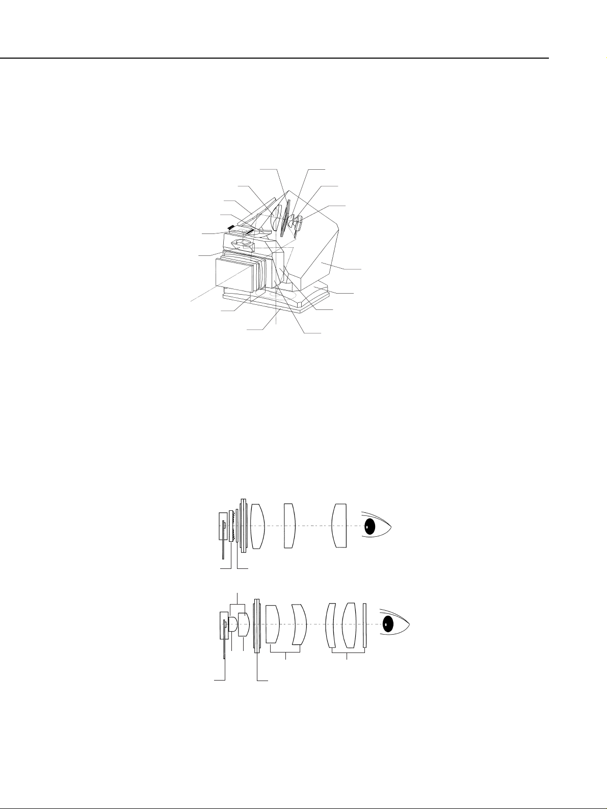
2) Superimposition display optics
Except for not having a dichroic mirror between the pentaprism and eyepiece
lens, the SI display optics (Fig. 2-10) for the focusing points are basically the
same as the EOS-3’s. The improvements are a brighter SI display and an SI display that is easier to see (Fig. 2-11).
● Display brighter by over 2 stops
The backlight optics uses a direct system (lens × 2) instead of a diffusion system
(fresnel lens + diffusion panel). It eliminates the light loss inherent with the fresnel lens and diffusion panel and increases the display brightness by over 2 stops.
● Clear SI display
By incorporating an aspherical surface for backlight lens 2 and the two SI lenses
(focusing point image-forming lens), a clear SI display with minimal aberrations is
obtained.
2-8
Part 2: Technical Information
Focusing screen
Eyepiece lens
SI lens 1
SI lens 2
SI-LED
Pentaprism
Condensor lens
SI prism 1
SI prism 2
Backlight lens 1
Backlight lens 2
SI mirror
Metering sensor
Metering lens
SI-LCD
Fig. 2-10 SI display optics.
SI-LED
12
SI-LCD
SI lens Eyepiece lens
Fresnel lens
Diffusion panel
Backlight lens
EOS-3
EOS-1V
Fig. 2-11 Comparison with the EOS-3’s SI display optics.
1.3 Exposure Control
1) Metering
(1) Metering optics and the AE sensor
The EOS-1V’s metering optics (see Fig. 2-10 on the preceding page) are positioned
above the eyepiece lens to avoid obstructing the SI display optics.
Evaluative metering and E-TTL autoflash use a new algorithm. Otherwise, the
other sensors and metering methods have the same specifications as the EOS-3’s.
(2) Evaluative metering
The EOS-3’s 21-zone evaluative metering system has
won high praise. However, a few users have pointed
out that the exposure can become inconsistent when
the picture is recomposed slightly. The EOS-1V uses a
new algorithm so that a more consistent exposure is
obtained with 21-zone evaluative metering while automatic exposure compensation (a strong point of the
EOS evaluative metering system) remains intact.
● EOS-3’s evaluative metering system
The EOS evaluative metering system hitherto centered
the main metering area around the active focusing
point and executed automatic exposure compensation
for the different brightness (mainly the differ ence with
the backlight areas) of the adjacent and peripheral
areas. However, since the EOS-3’s main metering area
is almost as narrow as the spot metering area, shifting
the main metering area even slightly can cause the
automatic exposure compensation amount to change
(Fig. 2-12). Thus, the exposure setting can change
even with a slight change in the subject framing. Also,
during continuous shooting of a moving subject with
AI SERVO AF and automatic focusing point selection,
the resulting exposures tended to be irregular in the
same series of continuous shots as the focusing point
shifted to next one. The shifting focusing point also
shifted the main metering area, causing the meter
reading to change.
● EOS-1V’s evaluative metering system
The EOS-1V’s evaluative metering system is linked to
and weighted on the active focusing point and the
meter reading is averaged (Fig. 2-14). Automatic exposure compensation is set for bright subjects. In effect,
the manual exposure compensation set for a bright
background during centerweighted averaging metering
has been replaced by focusing point-linked automatic
exposure compensation.
In other words, evaluative metering is now weighted
less on the active focusing point’s metering area. This
makes the exposure more consistent even when the
framing is changed slightly.
When focus is achieved at the desired location with a manually-selected focusing
point in the One-Shot AF mode, it is highly likely that the main metering area will
cover the main subject completely. Therefore, if the main metering area’s brightness level is still low after the automatic exposure compensation for a bright
2-9
Part 2: Technical Information
The main metering
The main metering area covers
the subject completely.
The main metering area is shifted to
cover the subject partially.
Fig. 2-12 EOS-3’s evaluative
metering system.
Fig. 2-13 Metering pattern for
centerweighted metering.
background, conventional
evaluative metering is
applied for backlight exposure compensation to suit
the main metering area’s
brightness level (see Table
2-3). Backlight exposure
compensation is applied
mainly under cloudy conditions, daylight shadows, and other backlit conditions when exposure compensation for a bright subject is not likely to be applied.
Evaluative metering is executed in the following steps:
q The metering is averaged while weighted on the focusing point and correspond-
ing metering area. If the active focusing point is on the border of the metering
area, the metering area with a less bright meter reading is selected as the
focusing point’s corresponding metering area.
w If the metered value is higher than the stipulated brightness level, several adja-
cent bright areas are sampled starting with the brightest area. If the metered
value is lower than the stipulated brightness level, conventional evaluative
metering is applied. The value obtained in q is used as the final reading.
e The sampled bright areas are averaged and a positive amount of exposure com-
pensation is added.
r With manual focusing point selection + One-Shot AF, backlit exposure compen-
sation obtained with conventional evaluative metering is also applied if the
subject’s brightness level at the main metering area is still low even after exposure compensation for a bright subject is applied.
● Evaluative metering for consistent exposures and easy detection of required exposure
compensation
This evaluative metering uses a relatively simple algorithm which weights the
metering relatively lightly on the active focusing point and corresponding metering
area and mainly compensates for high-level brightness instead. Thus, a proper
exposure is obtained consistently even if the framing is slightly altered. For users
who mainly use centerweighted averaging metering, it makes it easier to see how
exposure compensation is applied.
Fig. 2-14 Sample metering patterns of focusing point-weighted averaging metering.
2-10
Part 2: Technical Information
Table 2-3 Conditions for evaluative
metering and exposure compensation.
Manual Focusing Automatic Focusing
Point Selection Point Selection
ONE SHOT AF
Brightness compensation
Brightness
+ Backlit compensation
compensation only
AI SERVO AF Brightness compensation only

Partial and spot metering coverage
Since the EOS-3’s viewfinder coverage is 100% instead of 97%, the partial and
spot metering coverage has become slightly smaller. However, if you round off the
figure to the second decimal place, it becomes the same as the EOS-3. Thus, the
EOS-1V’s partial and spot metering coverage is the same as the EOS-3’s at
approx. 8.5% for partial and 2.4% for spot metering. (These are official specifications.)
3) E-TTL autoflash
To obtain a more consistent flash exposure, the main flash output calculation
algorithm has been changed.
With the EOS-3, the main flash output is determined by the preflash reflected off
only the areas covered by the main flash metering area (covering the main subject) and adjacent flash metering areas. Thus, if the picture is even slightly
recomposed, a different flash exposure (Fig. 2-15) may result as in the case of
evaluative metering.
With the EOS-1V, preflash meter readings are taken from the main flash metering
area covering the main subject and from a peripheral group of flash metering
areas (Fig. 2-15 - q ) which received the brightest r eflectance. The metering weight
of the main flash metering area and the weight of the brightest peripheral group
are averaged to determine the main flash output. Since the peripheral group covers a larger area than with the EOS-3, the algorithm selects a more consistent
flash exposure level even if the framing changes slightly.
During automatic focusing point selection, the metering is weighted more on the
peripheral flash metering area than on the main flash metering area. This results
in a more consistent flash exposure level even if the subject framing is changed
slightly. In the case of manual focusing point selection, it is more likely that the
entire main flash metering area will cover the subject. Therefore, the metering is
weighted more on the main flash metering area than on the peripheral flash
metering area.
If a peripheral flash metering area receives an abnormally high preflash
reflectance, the peripheral flash metering area expands (Fig. 2-15 - w ) and the
metering weight is averaged with the weight of the main flash metering area. The
main flash output is thereby determined.
2-11
Part 2: Technical Information
q E-TTL autoflash metering areas
w E-TTL autoflash metering areas for abnormally high preflash reflectance.
Fig. 2-15 Grouping of peripheral flash metering areas
2) Exposure control system
The EOS-1V’s exposure control is the same as the EOS-3’s.
2-12
Part 2: Technical Information
3) Exposure control mechanism
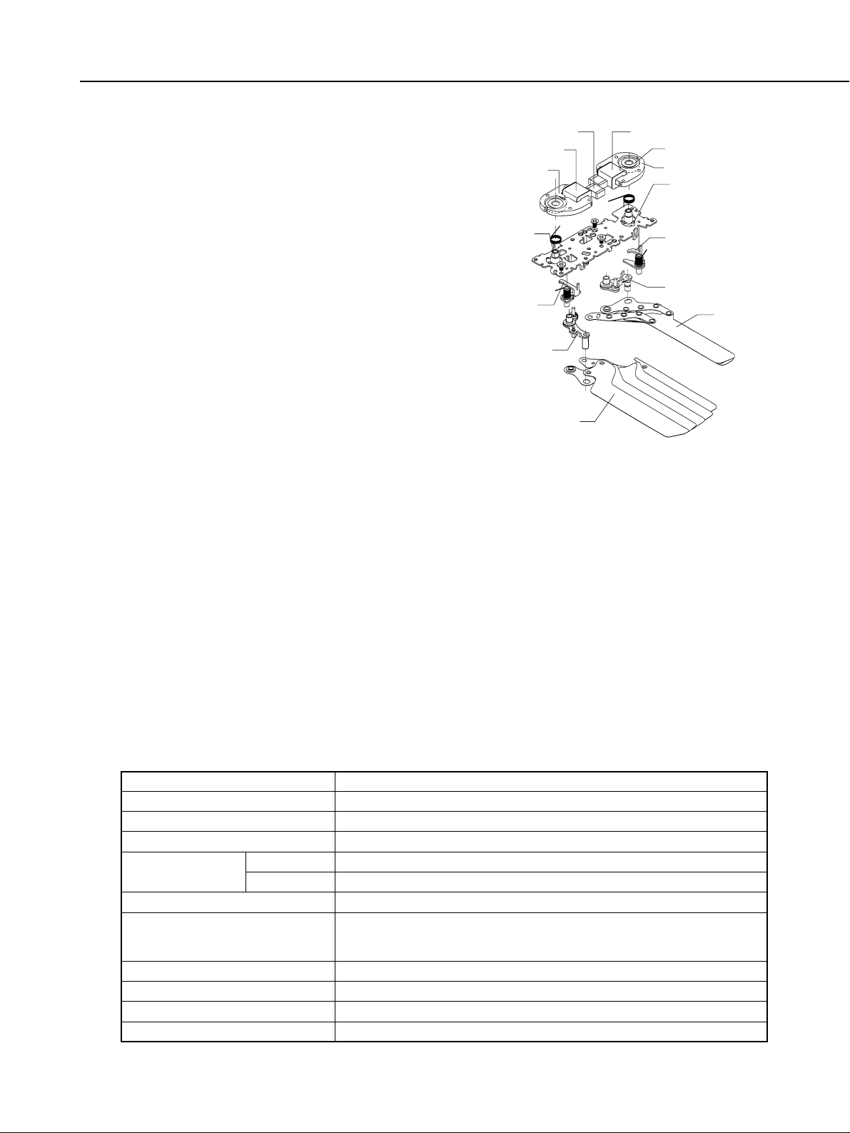
(1) Shutter
While based on the EOS-3’s shutter, the
EOS-1V’s shutter (made by Canon) features improved basic perfor mance, reliability, and durability. The official shutter durability specification is 150,000
cycles. In actual tests, the shutter lasted up to 200,000 cycles. The operation
principle, unit appearance, and the
maximum bulb exposure time (1,000
hr) are all the same as the EOS-3’s
shutter.
q Improved shutter curtain-driving
spring and coil for faster operation
A more powerful shutter curtain-driving spring and coil (Fig. 2-16)
enables the maximum shutter speed
of 1/8000 sec. and maximum X-sync
speed of 1/250 sec. (curtain speed of
2.2 ms/24 mm).
w Higher precision
To enhance precision, the motor shaft now has a different shape, material, and
surface finish to lower friction and the shape of the release lever has been
changed.
e Carbon fiber shutter curtains for better strength and durability
The slit-producing shutter curtains are made of carbon fiber to make the curtain unit lighter, stronger, and more durable.
r Anti-friction material and surface finish for better durability
To improve durability, the rotating shafts and bearings of all drive levers are
now made of a material and surface finish having excellent anti-friction properties.
t Stronger shutter curtain braking for added durability
To cope with the faster shutter curtain drive speed, the curtain brake mechanism is now stronger for better durability.
Table 2-4 Shutter Design Specifications
2-13
Part 2: Technical Information
Fig. 2-16 Exploded view of shutter unit.
Item
1. Type
2. Shutter curtain system
3. Shutter curtains
4. Shutter curtain
material
5. Curtain driver
6. Shutter speed control
7. Curtain speed
8. Shutter speed range
9. Max. flash sync speed
10. Signal
Design Specifications
Vertical-travel, focal-plane shutter
Rectangular, parallel-linked type
1st curtain: 5, 2nd curtain: 5, total 10
2 curtains made of carbon fiber, 3 curtains made of ultra-duralumin
2 curtains made of carbon fiber, 3 curtains made of ultra-duralumin
1st and 2nd curtains each have two dedicated torsion springs
All speeds electronically controlled by controlling the conduction of power
to the dedicated magnets for the 1st and 2nd curtains,
(Magnet type: Newly-developed, rotary magnet)
Approx. 2.2 ms/24 mm
30 - 1/8000 sec., bulb
1/250 sec.
Two types: q X-sync and w 2nd-curtain synchronization
1st curtain
2nd curtain
Coil (for 2nd curtain)
Yoke (for 2nd curtain)
Magnet × 2
Cam (for 2nd curtain)
2nd curtain fixed lever
2nd curtain drive lever
2nd curtain
1st curtain
1st curtain drive lever
1st curtain fixed lever
Cam (for 1st curtain)
Yoke (for 1st curtain)
Coil (for 1st curtain)
Chip condensor × 2
1.4 Film Transport
● High-power film advance motor M1, ● film advance with floating support, and
● a film transport detection system compatible with infrared film. Other features
are the same as with the EOS-3 (see the EOS-3’s Technical Information Part 2).
1) High-power, film advance motor
The EOS-3 uses a motor having a rated voltage of 6 V. The EOS-1V uses the
same high-power, 12 V motor as the EOS-1N. And with the 12 V power supplied
directly by the PB-E2, the EOS-1V can attain a continuous shooting speed of 10
fps.
The difference between the motors used in the EOS-3 and EOS-1V lies in the
design concept. The EOS-3 provides adequate performance even
without the PB-E2. It uses a 6 V
motor to match the 2CR5 6 V battery used when the EOS-3 is powered internally. Whereas the EOS1V was primarily designed to attain
maximum performance with the
PB-E2 attached. It therefore uses a
12 V motor. See Table 15 for the
speed difference with and without
the PB-E2 for both cameras.
● Preconditions to attain 10 fps
The PB-E2 and NP-E2 are attached
and the lens EMD stopdown time is
35 ms or shorter (equivalent to 2
stops worth with the EF 300mm
f/2.8L IS USM). If the aperture is
stopped down, farther the continuous shooting speed decreases due
to the increased EMD stopdown
time. The continuous shooting
speed does not differ with different
lenses.
2-14
Part 2: Technical Information
Table 2-5 Maximum Continuous
Shooting Speed (fps)
M-1: Dedicated motor
for film advance
M-1: Dedicated motor
for film advance
Guide roller 1
M-2: Cocks the shutter and quick-return reflex mirror
and rewinds the film
Guide roller 2
Guide roller 2
Guide roller 1
M-2: Dedicated motor for film rewind
M-3: Cocks the shutter and quick-return reflex mirror
Lo planetary gear
Hi planetary gear
(2) Three-motor system with PB-E2 attached
(1) Two-motor system (without PB-E2)
Fig. 2-17 Film transport system.
Camera only
PB-E2 + NP-E2
EOS-1V
3.5 fps
10 fps
EOS-3
4.3 fps
7 fps
2) Silent film advance
The floating supports at four places (Fig. 2-18) in
the film advance unit have reduced the film
advance noise and vibration (Table 2-6). The shutter cocking system’s floating supports also help to
reduce the continuous film advance noise.
● Discernable noise cut by half with low-speed cocking
With the Personal Function PF-21 “Silent (lowspeed) film advance after film is exposed and
shutter button turns off,” silent film advance is
possible with the EOS-1V (without PB-E2) set to
single-frame advance.
The noise level is 5 dB lower than the standard
cocking noise which is about half the discernable
noise level (Table 2-7). Also, since low-speed film
advance suppresses the high-frequency range (4 - 8 KHz), it actually sounds
much quieter. With mirror lockup, the noise comes from only the shutter, making
it even more quiet. It is suited for when noise is unwanted.
By employing a slow speed (the film advance speed is unchanged) for cocking the
shutter and mirror which usually makes a large noise, the operation is quieter.
The M2 motor’s PWM control and silent rewind have been applied to the cocking
of the shutter and mirror.
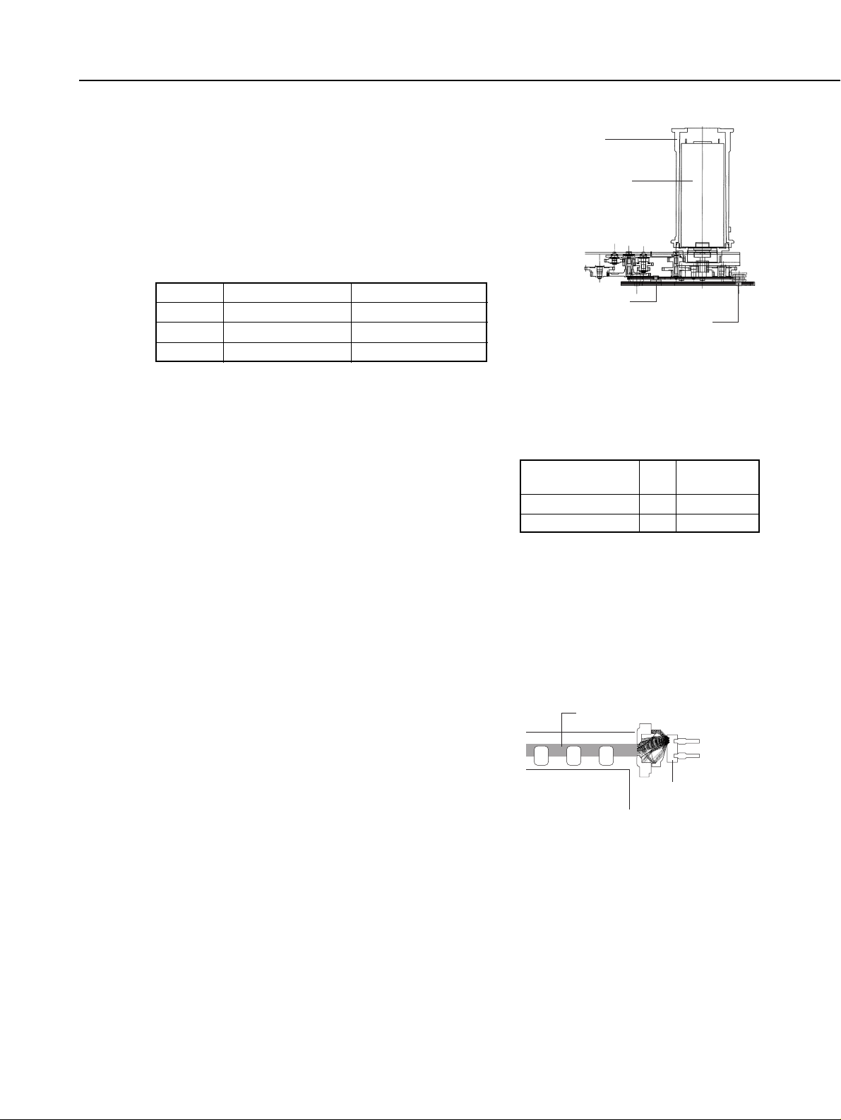
3) Film transport detection system
● Compatible with infrared film
The film perforation is detected optically with a
photo reflector (Fig. 2-19). The upper half of the
perforation is detected by condensor optics.
Masking material is used to shield the picture area
against the infrared light. This enables infrared film
to be used. Also, the light reception efficiency has
been improved with the condensor optics, and the
infrared light intensity has been reduced to further
decrease the chances of fogging the film.
2-15
Part 2: Technical Information
Fig. 2-18 Film advance unit’s
floating supports.
EOS-1V
EOS-3
EOS-1N
Continuous Shooting
79.2 (7)
87.1 (7)
78.9 (6)
Single-Frame Shooting
76.2
77.8
79.7
Table 2-6 Comparison of shutter release and film
advance noise in dB (fps)
Standard Cocking
Low-speed Cocking
Noise
67
62
Film Advance
time
0.46
0.73
Table 2-7 Comparison of cocking noise
(dB) and time (sec.)
Fig. 2-19 Film transport
detection system.
Rubber bushing × 1
Rubber bushing × 3
Spool
M1:
Film advance motor
Infrared film fogging area
Photo reflector for film
transport detection

1.5 Overall Operation
1) About high-speed continuous shooting
With high-speed sequence control and quick mirror bound suppression, the EOS1V attains 10 fps in the One-Shot AF mode with real-time AE metering for each
shot. (The EOS-1N RS attains 10 fps only with AE lock and a stopped-down aperture.) In the AI Servo AF mode, the AF-dedicated, high-speed microcomputer
enables a speed of 9 fps, the world’s fastest.
* AEB at 10 fps is also possible (not possible with the EOS-1N RS).
q High-speed sequence control with the PB-E2 and NP-E2
With the PB-E2 and NP-E2 attached to the camera, high-speed drive is
achieved with the M-1 motor (film advance) operating at 12 V, the M1 system
set to Hi gear, and the M-3 system (cocking) set to Hi gear. In the AI Servo AF
mode, the lens is driven simultaneously during all sequences except when the
shutter is opening or closing (as with the EOS-3). This enables faster speed as
well as better predictive AF and subject tracking.
w Mirror bound suppression with the mirror
down/lockup mechanism
The mirror lockup mechanism consists of a
mirror hook and a locking pin on the camera (Fig. 2-20). When the main mirror is
down, it is locked. In the mechanical
sequence, the most unstable element is the
mirror bound that occurs when the main
and secondary mirrors go down. The mirror bound has been suppressed to 45 ms
or less (Table 2-8) in all camera orientations. The continuous shooting speed has
been improved with a quick AF and AE
transition, the viewfinder blackout time
has been shortened, and the viewfinder
image does not shake after the main mirror goes back down.
e 32-bit RISC microcomputer for high-speed
processing
The high-speed, 32-bit RISC microcomputer is dedicated to AF processing and data
memory. It operates at a clock speed of
33.3 MHz (EOS’s fastest) for high-speed
processing.
2-16
Part 2: Technical Information
Locks
DOWN
UP
Released
Mirror hook
Locking pin
Locking arm
Fig. 2-20 Mirror down/lockup mechanism.
EOS-1V
EOS-3
EOS-1N
Mirror-down
Stabilization Time (ms)
45 or less
65 or less
80 or less
Viewfinder
Blackout Time
87
105
140
Table 2-8 Mirror-down stabilization time and
viewfinder blackout time (ms)

2) Stabilizing the continuous shooting interval
q Stable and secure focusing operation with the mirror -stabilizing timer
The main and secondary mirrors give an inconsistent down stabilization time
depending on the camera’s orientation. To resolve this problem, the sequence
has been extended slightly and the timer control has been set so that it goes to
the next focusing sequence after the longest mirror stabilization time elapses.
In other words, even if the mirror bound ends sooner, the focusing operation
remains on standby until the set time elapses. With a regular and proper transition to the next focusing sequence, the continuous shooting interval becomes
consistent and stable. Since this also stabilizes the focusing interval during the
continuous sequence, it enables a more precise statistical operation than when
the preceding focusing data is used.
w Even after the lens drive ends, exposure does not start until the set time elaps-
es
In the 9 fps continuous shooting sequence, even if the lens drive has ended,
the exposure will not start until the set time elapses. By absorbing any inconsistent lens drive time in this way, the continuous shooting interval and focusing interval become consistent. This in turn enables accurate statistical operation.
When (1) and (2) above are applied together, a stable operation sequence with
minimal adverse effect on picture-taking is obtained. In previous cameras, the
sequence control was for maximum speed. With the EOS-1V, all the unstable elements affecting the AI Servo AF continuous shooting speed such as the mirror
operation, focusing, and lens drive are eliminated with a time out and timer control.
3) Data communication
Communication between the EOS-1V and EOS Link Software ES-E1 via the
remote control/communications terminal use the same bi-directional communication system used between the EOS camera and EF lens. The EOS Link Software
ES-E1 communication cable’s signal converter converts the signal into one compatible with USB/EOS. Communication between the EOS-1V and PB-E2 are the
same as with the EOS-3.
4) Shutter release mechanism
The EOS-1V’s shutter release mechanism
uses a two-step switch. At SW-1 ON,
metering and focusing are executed. At
SW-2 ON, the shutter releases and the picture is taken. Table 2-9 shows the shutter
button stroke and pressure. Besides the
button’s standby height and SW-1 ON
stroke, service personnel can also adjust
the stroke between SW-1 and SW-2.
2-17
Part 2: Technical Information
Position
Standby to SW-1 ON
SW-1 ON to SW-2 ON
Beyond SW-2 ON
Stroke
0.6 mm
0.3 mm
0.2 mm
Pressure
85 g
350 g
—
Table 2-9 Shutter Button Stroke and Pressure

Figure 2-21 shows a flowchart for the overall operation sequence, and Fig. 2-22
shows the overall operation’s timing chart.
Precondition: EOS-1V + PB-E2 + USM lens, AI Servo AF mode, new batteries
Fig. 2-21 Operation sequence flowchart.
2-18
Part 2: Technical Information
Initialization
Battery loaded
Ready
Shutter capacitor
charging ON
SW-1 and SW-2
ON?
N
Y
AE metering calculation
SW-1
ON?
N
Y
N
Y
AF calculation
Lens driven
Meter timer
ON?
Normally
approx. 6 sec.
After exposure,
approx. 2 sec.
SW-2
ON?
Self-timer?
N
Y
Y
N
Self-timer operates
BC
EMD stops down
Mg-2 ON/OFF
Mirror goes up
Shutter capacitor
charging OFF
Shutter capacitor
charging ON
Mg-3-1 ON
Exposure starts
Exposure time control
Mg-3-2 ON Exposure ends
M-1 powered
EMD at maximum
aperture
Film advance
AE metering calculation
AF calculation
Mg-2 ON
Lens driven
SW-2
ON?
N
Y
Wait until film advance ends
BC
EMD stopped down
Mg-2 ON/OFF
Mirror
goes up
: Indicates simultaneous control
: Indicates transition to the
next step after all preconditions
are met.
Control sequence for the 1st shot
Continuous shooting sequence for the 2nd and subsequent shots

2-19
Part 2: Technical Information
SW-2
Mg-2
Mirror operation
Mg-3-1
Mg-3-2
Mirror stabilization timer
EMD
CLOSE CLOSE
OPEN
M-1
M-2
M-3
Lens driven
Metering and focusing
10mS
0
50
100
150
200
mS
Writing of shooting data
Lens driven
For one frame during approx. 9 fps continuous shooting
AF and AE
Lens driven
Film advance, mechanical cocking
Mirror goes down
Actual exposure
Stop down
Mirror goes up
←At 10 fps: Reduced according to the stabilization timer for secondary mirror
←At 10 fps: Reduced according to the AF processing time
Precondition: EOS-1V + PB-E2 + NP-E2 (fully charged), USM lens, AI Servo AF mode, ultra-high speed continuous shooting, AF
achieved, SW-2 ON after SW-1 ON
Fig. 2-22 Overall operation timing chart.
UNAPPROVED REPRODUCTION RESTRICTED

1.6 Electronic Circuitry
1) Overview
The electronic circuitry centers on three CPUs. Other components include twelve
LSIs and ICs, a quartz oscillator, and display elements. AF calculation is based on
a high-speed reference clock running at 33.3MHz. Overall camera operation is
based on an 11.059 MHz clock pulse. Fig. 2-24 shows the circuit block diagram.
2) Three CPUs
The CPU dedicated to the AF and data memory is a high-speed, 32-bit RISC
microcomputer. The CPU for AE calculation, display, and sequence control is a
16-bit CISC microcomputer. There is also a CPU for the film ID imprinting module. Each CPU is independent and each operates in parallel simultaneously. Table
2-10 shows the specifications of the three CPUs.
Table 2-10 Specifications of CPUs
2-20
Part 2: Technical Information
Item
1. Main clock
2. Fastest calculation speed
3. Commands
4. Computing power
5. Internal registers
6. ROM
7. RAM
8. EEPROM
9. Timers
AF, Data Memory
CPU V853
33.3 MHz
0.03 µs
74
Add./sub./div.: 32 bit
Mult: 16 × 16 → 32 bit
32 bit × 32
256 KB (flash)
8 KB
—
16 bit × 16
Main CPU
MC68HC912E56
11.059 MHz
0.18 µs
211
Add./sub./div.: 16 bit
Mult: 16 × 16 → 32 bit
16 bit × 5
56 KB
2 KB
2 KB
16 bit × 8
Imprinting Module
CPU µ PD753104
4.19 MHz
0.95 µs
48
Add./sub.: 8 bit
16 bit × 5
4 KB
2 KB
—
8 bit × 5

2-21
Part 2: Technical Information
Fig. 2-23 Block diagram of circuit.
OSC
Display panel illumination EL
Focusing point LED
Viewfinder LED × 3
Film transport detection sensor
Display panel LCD
Focusing point LCD
Viewfinder V-LCD
Viewfinder H-LCD
Self-timer LED
M1
M2
Motor driver 1
Motor driver 2
Input of information
Mg3-1, Mg3-2
Shutter
Shutter DC/DC
Main DC/DC
Imprinting
module
Main CPU
LCD driver
Clock
OSC
Backup super
capacitor
Mg2
AF-CPU
BP-CPU
Electronic beeper
OSC
AF sensor
OSC
EEPROM
Camera
orientation
sensor
DX code
To camera
components
Flash metering
sensor
Metering sensor
SW-2
SW-1
Standard camera
back
To camera components
Direct contacts
Remote switch
ES-E1
Remote control /
Communication terminal
Direct contacts
Dedicated Speedlite
EOS-1V
Electronic mount
USM/AFD EMD
Pulse board
LENS µ-COM
Focal point detection information
Macro information
Focus mode
Control IC
EF lens
BP-E1
Power source
2CR5
Power source
LR6 × 4
Grip
Power source
2CR5
PB-E2
DC/DC
converter
Power source
LR6 × 6
Ni-MH
PB-MPU Motor driver 3
SW electronic lock
SW-1 / SW-2
M3
Bi-directional transmission
Direct contacts

1.7 Internal Construction
1) Covers
● Magnesium alloy covers
The top and front covers (Fig. 2-24) are
made of magnesium alloy which is
lightweight and very strong. Besides the
high-strength exterior, the camera’s
overall rigidity has been improved and it
also shields against electromagnetic
fields at the same time.
Thixotropic mold technology* is used to
manufacture the EOS-1V’s magnesium
alloy covers. With this method, the
three-dimensional curves of EOS-1series cameras are reproduced on the
metal exterior.
Also, the magnesium alloy cover is
painted in black with electrodeposition.
This coat is further covered by three more coats of black baked on the surface.
This tough surface finish make it less prone to paint wear or exposure of the
magnesium alloy.
The other exterior covers are made of engineering plastic while the proper
strength and precision are still attained. The camera’s bottom cover is made of
engineering plastic instead of metal since a metal bottom would add little to its
strength due to the shallow structure.
* Thixotropic mold technology
This is a hybrid method that combines
metal diecast molding technology and
plastic injection molding technology. It
enables magnesium alloy to be molded
into complex, curving, three-dimensional surfaces with high precision and high
density (prevents air bubbles from mixing in) as with plastic.
The molding procedure is as follows
(refer to Fig. 2-25): q . Similar to plastic
injection molding, magnesium pellets
are supplied by a hopper. w . The shearing force of the screw and cylinder
makes it thixotropic, a solid-liquid
state. (Thixotropy is a state when the mold material becomes a mixture of solid
and liquid due to a large shearing force that increases the fluidity.) e . The mold
material is injected into the mold to shape the part.
If the mold material is melted and then injected into the diecast mold, the material inside the mold becomes an irregular mixture while filling up the mold. When
there are complex, three-dimensional curves or minute shapes, air bubbles are
prone to form in the part being molded. Achieving production consistency for the
part then becomes a problem. Whereas with thixotropic molding, the mold material enters the mold uniformly with few air bubbles. Production then becomes consistent.
2-22
Part 2: Technical Information
Fig. 2-24 Magnesium alloy covers.
Hopper
Feeder
High-speed jet stem
Screw
Rotary drive
Cylinder
Nozzle
Mold
Heating zone
Fig. 2-25 Thixotropic mold technology.

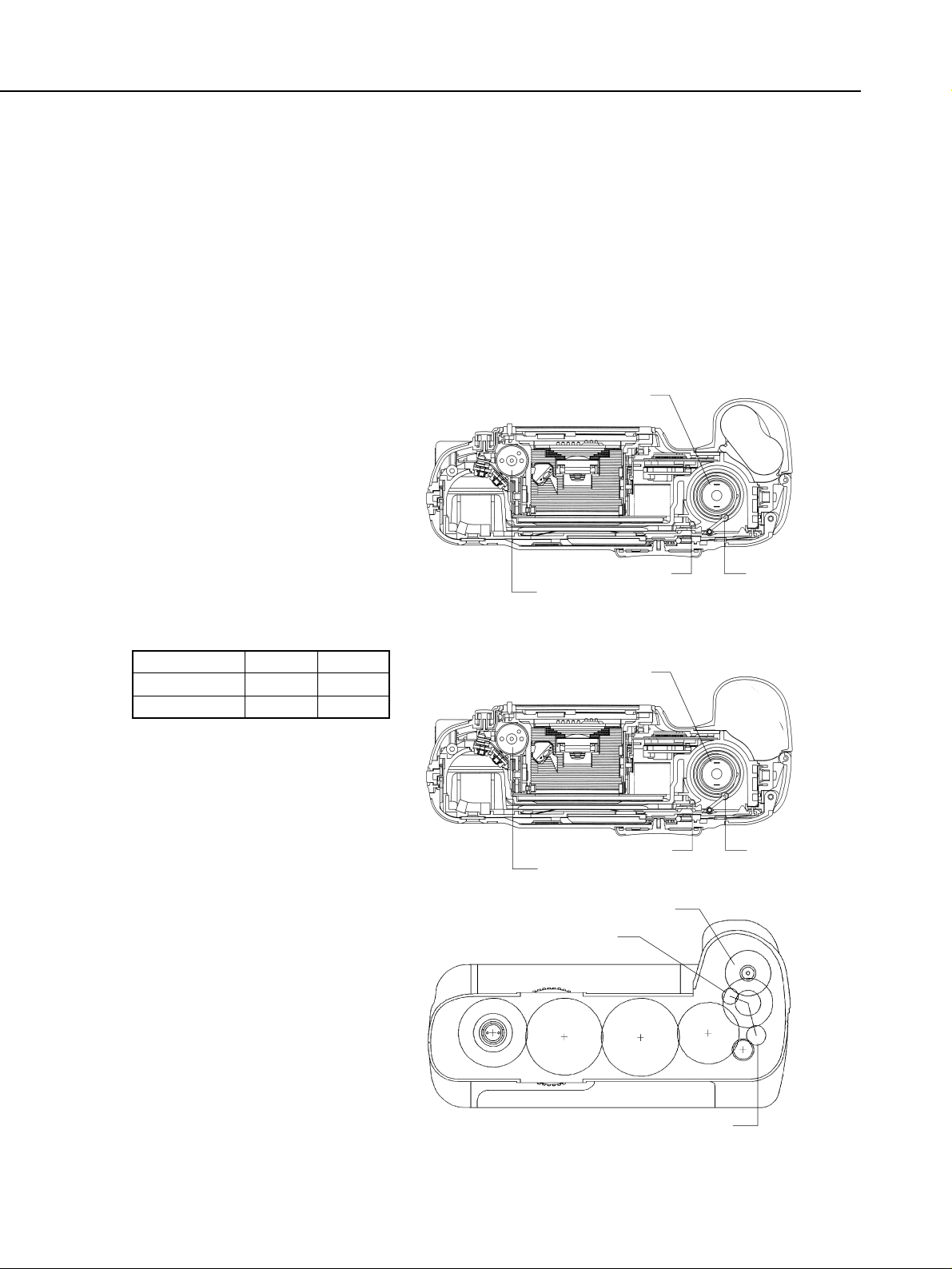
2) Internal construction and parts
location
The main chassis is molded from polycarbonate resin with glass fiber. The
critical film aperture is made of die-cast
aluminum and insert molded into the
chassis. The front panel that, together
with the aperture section, determines
the critical flange to focal plane distance (FFD) is also made of die-cast
aluminum (Fig. 2-27).
Table 2-11 gives the parts count, and
Fig. 2-28 locates the major components.
● Even with multiple quantities of the
same part, each is counted individually.
● Lead wires are also counted as elec-
trical parts.
● The shutter unit is counted as one
part.
● The official parts count excludes screws and washers.
Fig. 2-28 Location of major components.
2-23
Part 2: Technical Information
Fig. 2-26
Fig. 2-27
Mechanical Parts
Screws and washers
Electrical parts
Total
Official total
678
185
461
1324
1139
Table 2-11 Parts Count
Pentaprism
Metering sensor
Viewfinder H-LCD
Viewfinder V-LCD
Film advance mechanism
Main reflex mirror
Secondary mirror
DX code detector
M2 motor
Shutter cocking mechanism
TTL metering sensor
Electronic mount and data transmission
signal contacts
AF unit
Film rewind gear train
Shutter speed control mechanism
System connector
Lithium battery 2CR5
M1 motor
Main Dial
External LCD panel
Quick-return mirror mechanism
Focusing screen
Condensor lens
SI unit

3) Water- and dust-resistant construction
To make the EOS-1V the most water - and dust-resistant SLR camera of all (other
than underwater cameras), a total of 72 locations on the exterior covers and camera controls have been made to resist water and dust.
Also, the camera back and battery compartment cover are lined with packing, and
the top cover and buttons are sealed with silicone* rubber to prevent water and
dust from entering. These countermeasures are visible to the user to give him/her
a sense of security. Water- and dust-resistant measures are featured in the following major locations:
q Push buttons and switches ...... 16
For buttons like those on the left shoulder having a gap
between the exterior cover and the button, a silicone rubber cover is used to seal the perimeter around the buttons (Fig. 2-29). For switches like the shutter button and
FE lock button which have no such gap, a silicone rubber boot is fitted under the button.
w Rotating parts ...... 6
O-rings have been fitted around the Main Dial, Quick
Control Dial, dioptric adjustment knob, and eyepiece
shutter lever (Fig. 2-30) where it is relatively easy for
moisture to seep inside. A high-friction sheet is sealed
around the shafts of the main switch and Quick Control
Dial switch.
e Closing/opening parts ...... 3
The camera back and battery compartment cover are
lined with a silicone rubber packing (Fig. 2-31).
r Exterior cover seams ...... 36
A silicone rubber sheet is used to seal the major seams (20). Silicone, waterproof material, and an adhesive coat are used at 10 seams. And washers are
used for six exterior screws.
t Grip attachment surface and other exter nal inter faces ...... 10
To maintain the EOS-1V’s water - and dust-resistance even while the PB-E2 or
BP-E1 is attached, the grip attachment surface and system connectors are
sealed with silicone rubber.
y Mount surface ...... 1
To match EF lenses having a water -resistant rubber ring on the mount, the
camera’s lens mount also has a matching, water -resistant ring.
* The difference between silicon and silicone: Silicon is the element (Si) and mate-
rial made of silicon crystals. It is used in silicon wafers, silicon solar cells, etc.
Silicone is made of a silicon compound and used in grease, rubber, and resins.
2-24
Part 2: Technical Information
Fig. 2-29 Rubber cover.
Fig. 2-31 Camera back packing.
Silicone rubber
O-ring
Fig. 2-30 Electronic dial.

Fig. 2-32 Major water-resistant locations
2-25
Part 2: Technical Information

4) Electrical components
To enable continuous shooting at 10 fps, the EOS-1V’s electrical circuitry is larger than the EOS-3’s. The DC/DC converter (reduces the shutter cocking time) and
M1 driver (high-power 12 V motor) circuitry is large, and there are also the clock,
data memory, and transmission circuit for EOS LINK Software ES-E1.
This large-scale electronic circuitry has been made to fit within the same body
size as the EOS-3’s thanks to the following technologies:
● High-density, 6-layer main flexible board
The 6-layer flexible board has three double-sided flexible boards stacked together.
This high-density, double-sided configuration with meticulous circuit wiring
resulted in a compact, main flexible board.
● BGA package for the main CPU
The compact, multi-pin BGA package used in the EOS 300/Rebel 2000/EOS Kiss
III is also incorporated in the EOS-1V. Even though the EOS-1V’s CPU has 169
pins, the package is smaller than the EOS-3’s main CPU equipped with 128 pins.
Centering on the main flexible circuit board, the electronic circuitry consists of 21
flexible boards, 15 0.5mm-pitch connectors, and 2 board connectors. This compact configuration makes assembly easy. Figure 2-33 shows the electrical system.
Fig. 2-33 Electrical system.
2-26
Part 2: Technical Information
Hot shoe
21-zone metering sensor
Metering flexible board
Super capacitor
SI-LCD flexible board
Sound element
LCD driver
V-LCD flexible board
Eye Control detection switch
Camera back flexible board
Film ID imprinting CPU
Film ID imprinting module
Quick Control Dial base
H-LED
M2 motor driver
V-LCD
V-LED
DX flexible board
Remote control flexible board
CGE board
H-LCD
Remote control /
Communications terminal
PC terminal
Main switch board
M2 motor
Main switch flexible board
External LCD panel
EL illumination element
Top flexible board
Display panel flexible board
SI-LED
SI-LCD
ADSW flexible board
Main Dial
Main Dial base
H-LCD flexible board
M1 motor driver
Main CPU
DC/DC flexible board
Grip flexible board
Main flexible board
Shutter speed control
mechanism
AF-CPU
M1 motor
Area CMOS focusing sensor
TTL 3-zone flash exposure sensor
Mount contacts
Mount flexible board
AF flexible board
Flash exposure flexible board
System connector

2. SWITCHES
(1) Operation Switches
2-27
Part 2: Technical Information
No. Code Name
1 SW1 Focusing/metering
2 SW2 Release
3 MAIN SW Main
4 AEL SW AE lock
5 FPSEL SW Focusing point selector
6 MODE SW Picture-taking mode
selector
7 AF SW AF mode selector
8 MES SW Metering mode selector
9 COMP SW Exposure compensation
10 LAMP SW LCD panel illumination
11 REW SW Manual rewind
12 SPDN SW Depth-of-field preview
13 DIAL1, 2 SW Electronic dial
14 C Fn SW Custom Function setting
15 Mn SW Extended function
16 ME SW Multiple exposure
setting
17 CLR SW Clear
18 FEL SW FE lock
19 ADD SW Assist button
Function
Starts autofocusing and metering.
Shutter release.
Camera on (Beeper ON selected).
AE lock applied. (AE lock also applied while meter-
ing is active.)
Enables manual focusing point selection with the
electronic dial (same as with EOS-3).
Shooting mode selection in combination with elec-
tronic dial operation.
AF mode selection in combination with electronic
dial operation.
Metering mode selection in combination with elec-
tronic dial operation enables. Also enables flash
exposure compensatin with Quick Control Dial
operation.
Enables exposure compensation to be set with the
electronic dial.
External LCD panel is illuminated. Illumination
continues while metering is active.
Film rewind begins even in midroll.
Metering starts and the aperture stops down in
accordance with the meter reading.
Operates in combination with other switches.
Shooting mode, AF mode, metering mode, etc.
Sets or cancels Custom Function settings.
Each time the button is pressed, it enables data
recording, clock setting, Personal Function settings, data transfer mode setting, etc. (Clock function works only after camera is connected to the
ES-El for the first time.)
Sets multiple exposures.
Clears all settings, which revert to the default settings.
FE lock/muiti-spot metering is applied.
Used in combination with Custom Functions and
extended functions.

(2) Status Switches
(3) Mechanical Switches
2-28
Part 2: Technical Information
No. Code Name
1 BP SW Camera back
open/close switch
2 PTIN SW Film cartridge-loaded
switch
3 BAT SW Reset switch
4 MIF SW Lens switch
5 SWBIRI SW Shock prevention switch
6 DX1-5 SW DX code switch
7 DX6, 7 SW DX code switch
Function
LOW when the camera back is open.
Detects whether or not film is in the camera.
OPEN when film is loaded.
Detects battery. OPENS when the battery is
installed, executing reset.
Detects if a lens is attached. CLOSED when lens
is attached.
Prevents shock from hot shoe when flash is connected to PC.
Detects ISO film speed.
Detects the number of exposures of the loaded film.
No. Code Name
1 MRUP SW Mirror up switch
2 CHG1, 2 SW Shutter-charge phase
switch
3 SWX SW X switch
4 CN2 SW 2nd-curtain switch
5 FILM1, 2 SW Film phase switch
Function
Detects when the mirror is in the up position.
Detects shutter charge, etc.
Triggers flash firing.
Detects completion of second shutter curtain's
travel.
Detects the film's frame count during film advance
and rewind.

3. MAJOR ELECTRICAL COMPONENTS
2-29
Part 2: Technical Information
No. Code Location (Unit)
1 MODULE BP
2 BPPU BP
3 TRBP2 BP
4 CBPU1 BP
5 RREG2 BP
6 RREG3 BP
7 RREG0 BP
8 PRESBP BP
9 RBP1 BP
10 RBP2 BP
11 CBPU2 BP
12 CREGBP BP
13 CRESBP BP
14 CRESBPIC BP
15 CREG1 BP
16 CREG2 BP
17 ZDBP BP
18 ZDBP2 BP
19 TRBP1 BP
20 TRBP3 BP
21 RESBPIC BP
22 VREGBP BP
23 BPFAR BP
24 RPRE BP
25 CBPU3 BP
26 ZDBP3 BP
27 RBPFAR BP
Function
LCD panel and lamp module for film ID imprinting.
Drives the MODULE and executes film ID imprinting in accor-
dance with instructions transmitted from the MPU.
Module imprinting lamp drive transistor.
BPPU power source VDD filter capacitor 1.
Module LCD panel bias resistor 2.
Module LCD panel bias resistor 3.
Module LCD panel bias resistor 0.
BPPU reset control pull-up resistor.
Module lamp drive voltage resistor 1.
Module lamp drive voltage resistor 2.
BPPU power source VDD filter capacitor 2.
Module LCD regulator bias filter.
BPPU reset terminal noise capacitor.
BPPU reset control IC power source filter capacitor.
Module LCD panel bias filter capacitor 1.
Module LCD panel bias filter capacitor 2.
Camera back contacts static charge protection Zener diode 1.
Camera back contacts static charge protection Zener diode 2.
Module LCD panel bias power source switch transistor.
Module lamp drive transistor 3.
BPPU reset control IC.
Module LCD panel bias regulator.
BPPU oscillator.
TRBP1 base resistor.
Camera back contacts static charge protection capacitor.
Camera back contacts static charge protection Zener diode 3.
BPFAR stability resistor (ensure oscillation under high temper-
ature and humidity).

2-30
Part 2: Technical Information
No. Code Location (Unit)
28 TRMG3-1 DC/DC
29 TRMG3-2 DC/DC
30 CDC1 DC/DC
31 CDC4 DC/DC
32 CSHDC1 DC/DC
33 CDC5 DC/DC
34 CDC6 DC/DC
35 CSHDC4 DC/DC
36 FUSE2 DC/DC
37 FUSE DC/DC
38 LSHDC DC/DC
39 LDC DC/DC
40 RDC5 DC/DC
41 RSEN2 DC/DC
42 RVCHK1 DC/DC
43 RSEN1 DC/DC
44 RVCHK2 DC/DC
45 RDC4 DC/DC
46 RSHDC5 DC/DC
47 RSHDC4 DC/DC
48 RPR1 DC/DC
49 RDC3 DC/DC
50 RCOMP3 DC/DC
51 RVB1 DC/DC
52 RSHV1 DC/DC
53 RSHV2 DC/DC
54 RDC2 DC/DC
55 RCOMP2 DC/DC
56 RPR2 DC/DC
57 RCN2 DC/DC
58 RDC6 DC/DC
59 RSHD1 DC/DC
60 RSHD3 DC/DC
61 RSHDC1 DC/DC
62 RSHDC2 DC/DC
63 RSHDC3 DC/DC
64 RSHD2 DC/DC
Function
Shutter drive transistor 1.
Shutter drive transistor 2.
DC/DC1 input filter capacitor.
DC/DC1 charge voltage storage capacitor.
Shutter DC/DC input filter capacitor.
REGVDD output filter capacitor.
REGE1 output filter capacitor.
Shutter DC/DC charge voltage storage capacitor.
Safety measure for VBAT.
Safety measure for VCHK line.
Shutter DC/DC step-up coil.
DCDC1 step-up coil.
DC/DC IC error voltage detection resistor (paired with RDC4).
Shutter DCDC output voltage MPU-monitoring resistor (paired
with RSEN1).
VCHK voltage MPU-monitoring resistor (paired with RVCHK2).
Shutter DCDC output voltage MPU-monitoring resistor (paired
with RESEN2).
VCHK voltage MPU-monitoring resistor (paired with RVCHKl).
DC/DC IC error voltage detection resistor (paired with RDC5).
SH-DC/DC IC error voltage detection resistor (paired with RSHDC4).
SH-DC/DC IC error voltage detection resistor (paired with RSHDC5).
PRFLMV input current limiting resistor. The current is (5-1.5-
0.1)/430 = Approx. 8 mA.
DC/DC IC error amp frequency characteristics improvement.
Creates the PRAD signal hysterisis (together with RCOMP1
and RCOMP2).
VBAT3 line leak-detection resistor.
Shutter drive capacitor load resistor. Paired with TRSHVI.
TRSHV2 base current-limiting resistor.
DC/DC IC oscillation frequency resistor. Paired with CDC2.
Creates the PRAD signal hysteresis (together with RCOMP1
and RCOMP3).
PRFLMV output current voltage transformer resistor.
CN2 signal pull-up resistor (terminals in the MPU do not have pull-up).
TRDC3 base resistor.
Shutter-driving circuit TRMG3-1 base current-limiting resistor.
Shutter-driving circuit TRMG3-2 base current-limiting resistor.
TRSHDC1 base current-limiting resistor.
SH-DC/DC IC oscillation frequency resistor. Paired with CSHDC2.
SH-DC/DC IC error amp frequency characteristics improvement.
Shutter-driving circuit TRMG3-1 base-emitter resistor to pre-
vent misoperation while the battery is removed, etc.

2-31
Part 2: Technical Information
No. Code Location (Unit)
65 RSHD4 DC/DC
66 RSHDC6 DC/DC
67 RCOMP1 DC/DC
68 RDC1 DC/DC
69 CCN2 DC/DC
70 CDC8 DC/DC
71 CDC9 DC/DC
72 CPR1 DC/DC
73 CPR3 DC/DC
74 C1M DC/DC
75 C2M DC/DC
76 CAMP2 DC/DC
77 CM1 DC/DC
78 CMTDR1 DC/DC
79 CPR2 DC/DC
80 CVPP DC/DC
81 CDC3 DC/DC
82 CSHDC3 DC/DC
83 CDC2 DC/DC
84 CSHDC2 DC/DC
85 ZDM1 DC/DC
86 ZDMD1 DC/DC
87 DDC1 DC/DC
88 DDC2 DC/DC
89 DSHDC DC/DC
90 TRDC2 DC/DC
91 TRE1ON3 DC/DC
92 TRVB2 DC/DC
93 TRE1ON1 DC/DC
94 TRE1ON2 DC/DC
95 TRPR1 DC/DC
96 TRSHV2 DC/DC
97 TRVCHK DC/DC
98 TRVB1 DC/DC
Function
Shutter-driving circuit TRMG3-2 base-emitter resistor to prevent misoperation while the battery is removed, etc.
SH-DC/DC IC control resistor. The driving starts when VBAT3
increases.
Creates the PRAD signal hysteresis (together with RCOMP2
and RCOMP3).
TRDC1 base current-limiting resistor.
CN2 line noise-reduction capacitor.
REGVDD output noise-reduction capacitor.
REGE1 E2 output noise-reduction capacitor.
PRFLMV output current voltage-transformed signal noise-
reduction capacitor.
MPU DA output PRDA signal noise reduction capacitor.
MTDR1 charge pump capacitor.
MTDR1 charge pump capacitor.
OPAMP2 power source filter capacitor.
Ml noise-control capacitor.
MTDR1 power source (El) filter capacitor.
PRFLMV power source (El) filter capacitor.
MTDR1 charge pump terminal voltage-retaining capacitor (15 V).
Capacitor for DC/DC IC error amp frequency characteristics.
Capacitor for SH- DC/DC IC error amp frequency characteristics.
DC/DC IC oscillation frequency capacitor. Paired with RDC2.
SH-DC/DC IC oscillation frequency capacitor. Paired with RDC2.
Ml (Hi film rewind) surge voltage-clamping Zener diode.
Zener diode as a motor driver latch-up countermeasure.
Suppresses reverse voltage caused by inductance of the lead
wire between VMl and MTDR1.
Shockley diode to prevent a reverse current from VDD to REG.
DC/DC1 rectification.
SH-DC/DC rectification diode.
Current cut-off transistor for current flowing to RDC4 and
RDC5 when DC/DC1 is off.
SHDC/DC control transistor.
Switch transistor turns on the TRVBL via MTDR1 when VBAT3
has no leakage or other problems.
DC/DC1 control transistor.
DC/DC1 control transistor. Since the standby current is elimi-
nated when the PDB is attached, TRE1ON1 and 2 are used.
Film signal photo reflector (FLMV) drive transistor.
Shutter-drive capacitor charge control transistor.
Switch transistor that turns on the PDB when El ON.
Power MOSFET connecting VBAT3 to VBAT.

2-32
Part 2: Technical Information
No. Code
Location (Unit)
99 TRSHDC1 DC/DC
100 TRDC3 DC/DC
101 TRSHV1 DC/DC
102 TRDC1 DC/DC
103 PWRAIC DC/DC
104 MTDR1 DC/DC
105 DC/DC_IC DC/DC
106
SH-DC/DC-IC
DC/DC
107 PWRDET DC/DC
108 REG DC/DC
109 OPAMP2 DC/DC
110 REGE1E2 DC/DC
111 REGVDD DC/DC
112 REGVDD2 DC/DC
113 DVDD DC/DC
Function
Shutter DC/DC switching-regulation transistor.
Switch transistor to prevent VDD flow to REGVDD input terminal.
Shutter-drive capacitor charging current transistor. Paired with
RSHV1.
DC/DC1 switching-regulation transistor.
Analog switch IC for power selection.
Ml (Hi, Lo film advance) motor driver IC.
PWM switching-regulator control IC (DCDC1 control).
PWM switching-regulator control IC (shutter DCDC control).
Reset IC (Active low, open drain output) for PWR2 detection.
The voltage detected is 4.2 V (only while PDB is attached).
Regulator IC that extracts 5 V from the VCHK output.
Comparator IC with hysterisis for the PRFLMV output current
voltage-transformed signal buffer (PRAD) and PRAD signal
and PRDA signal.
Regulator IC (4.8 V) for supplying El and E2.
Regulator IC (5.0 V) for supplying VDD.
VDD backup regulating IC when El OFF. Countermeasure for
lenses that consume a lot of power from standby.
Shockley diode to prevent reverse current from VDD to
REGVDD2.

2-33
Part 2: Technical Information
No. Code
Location (Unit)
114 RHLED1 DSP
115 RAFLED2 DSP
116 RHLED2 DSP
117 RPULLEL DSP
118 RAFLED1 DSP
119 DEL DSP
120 TREL2 DSP
121 TREL DSP
122 TRAFLED DSP
123 TRHLED DSP
124 LEL DSP
125 EL DSP
126 ZDM2 DX
127 C1M2 DX
128 C2M2 DX
129 CM2 DX
130 CMTDR2 DX
131 CVPP2 DX
132 ZDMD2 DX
133 MTDR2 DX
Function
HLED-drive transistor base resistor.
AFLED-drive, constant-current circuit resistor. (Set to approx.
5mA.)
HLED-driving, constant-current circuit resistor. (Set to approx.
35mA.)
TREL predriver output current-limiting resistor.
AFLED-drive transistor base resistor.
Negative-side protective diode for EL oscillating transistor
TREL collector when EF oscillates.
TREL predriver transistor. (With MPU direct PORT connection,
the TREL base current is insufficient.)
For oscillation. Wavelength: 732 us, 610 us On, 122 us OFF
(equivalent to 5/6 duty). Be aware of withstand pressure.
AFLED-drive transistor. Configured with RAFLED2 in a con-
stant-current circuit.
HLED-drive transistor. Configured with RHLED2 in a con-
stant-current circuit.
Resonates the EF step-up coil and EL equivalent capacity.
+160 V to -100 V (at VBAT=6.4 V).
Outside LCD backlight. Resonate frequency is about 23 KHz.
M2 motor (rewind, shutter cocking 6 V) surge voltage-clamp-
ing Zener diode.
MTDR2 charge pump capacitor.
MTDR2 charge pump capacitor.
M2 noise control filter.
MTDR2 power source (El) filter capacitor.
MTDR1 charge pump terminal voltage-retaining capacitor (15 V).
Zener diode as a countermeasure for motor driver latch-up.
Suppresses reverse voltage caused by inductance of the lead
wire between VM2 and MTDR2.
M2 (rewind, shutter cocking) motor-driving driver IC.

2-34
Part 2: Technical Information
No. Code
Location (Unit)
134 EFIC EF
135 CEF3 EF
136 RIREF1 EF
137 CRES2 EF
138 CE1 EF
139 CEFVC EF
140 CVBAT EF
141 CVRH1 EF
142 AF SENSOR GA
143 CGA2 GA
144 CREGIN GA
145 RG1 GA
146 RG2 GA
147 RGREG2 GA
148 RGREG1 GA
149 ROSC GA
150 RFIN GA
151 RG3 GA
152 RIRSP GA
153 CGDA1 GA
154 CGDA2 GA
155 CREGGA GA
156 CGA1 GA
157 CREG GA
158 CVGR GA
159 CVRS GA
160 GREG GA
161 REGGA GA
162 GFAR GA
Function
Flash metering sensor and flash communication IC.
EFIC power source (E2) filter capacitor.
Resistor that determines the EFIC IREF (for thermometers
constant current and external Speedlite flash-ready detection).
/RES2 signal noise-reduction capacitor.
EFIC power source (El) filter capacitor.
EFIC band gap voltage (VC=1.25 V) filter capacitor.
EFIC monitor voltage (VBAT) filter capacitor.
EFIC flash-metering reference voltage (VRH=3.2 V) filter
capacitor.
AF sensor with built-in I/0 function.
AF SENSOR power source (GVDD) filter capacitor.
REGGA input voltage filter capacitor.
Control signal line (READ, CSAF2, CSAF1 FOUT) pull-down
resistor from the AF SENSOR FPU.
Control signal line (CSAFO, DSEL, AFH, TCLK) ) pull-down
resistor from the AF SENSOR FPU.
GREG output voltage divider that produces VVC (1.20 V).
Paired with RGREG1.
GREG output voltage divider that produces VVC (1.20 V).
Paired with RGREG2.
AF SENSOR oscillation stabilization resistor.
AF SENSOR FPU transmission line (FIN) pull-down resistor.
AF SENSOR FPU transmission line (FCLK) pull-up resistor.
Constant-current circuit load resistor in the AF SENSOR.
DAC1 output filter capacitor.
DAC2 output filter capacitor.
REGGA output noise-reduction capacitor.
AF SENSOR power source (GVDD) filter capacitor.
AF SENSOR reference voltage (VVC) filter capacitor.
AF SENSOR reference voltage (VGR) filter capacitor.
AF SENSOR reference voltage (VRS) filter capacitor.
Regulator IC that produces the AF SENSOR VVC.
Regulator IC that supplies the AF SENSOR power source
(GVDD).
AF SENSOR Oscillator. The EOS-1 V uses a smaller pack-
age than the EOS-3.

2-35
Part 2: Technical Information
No. Code
Location (Unit)
163 RM3F2 GRIP
164 RDC2ON GRIP
165 RM3F1 GRIP
166 RMG21 GRIP
167 RMG22 GRIP
168 RM3HG GRIP
169 DMGM2 GRIP
170 DBAT GRIP
171 ZD1 GRIP
172 ZD2 GRIP
173 ZD3 GRIP
174 ZD4 GRIP
175 TRDATE1 GRIP
176 TRMG2 GRIP
177 CSDIAL1 GRIP
178 CSDIAL2 GRIP
179 HLED HLC
180 PIHV1 HV2
181 PIHV2 HV2
Function
Static discharge protection resistor.
VDD direct external output protection resistor. Also for
DCfDC2 ON-driving current limiting.
/M3F terminal PULL DOWN resistor. Also detects the attach-
ment of the normal grip. It has a high resistance to ensure
detection of the size-AA battery pack.
MG2-drive transistor TRMG2 base resistor.
Resistor between the MG2-drive transistor TRMG2 base-emit-
ter resistor.
PDB detector resistor.
MG2 (mirror up, down) coil reverse voltage prevention diode.
VCHK voltage (12 V) diode to prevent flow to the /RESMPU
line while the PDB is attached.
Static charge prevention Zener diode for camera back con-
tacts (MISOB, MOSIB, /DBUSY, SDIALL).
Static charge prevention Zener diode on SYSCON-2 terminal
(/M3HG, DIAL2, FEL, FPSEL).
Static charge prevention Zener diode on the camera back and
SYSCON terminal (SCLKB, M3F, SDIAL2).
Static charge prevention Zener diode on the SYSCON and
SYSCON-2 terminals (SW2, AEL, SW1, DIALL).
ID (and date) imprinting lamp-drive transistor.
MG2 (mirror up, down) drive transistor. Turns on for 8 ms dur-
ing mirror up, and mirror down operation.
DIAL1 signal static charge protection capacitor.
DIAL2 signal static charge protection capacitor..
Includes backlight LED for viewfinder horizontal LCD, 4-chip
LED (35 mA driving), and for AF in-focus LED1 chip (5 mA
driving).
Camera orientation sensor with integrated optical detection.
Camera orientation sensor with integrated optical detection.

2-36
Part 2: Technical Information
No. Code
Location (Unit)
182 MPU MAIN
183 FPU MAIN
184 CAMP1 MAIN
185 CAMPF1 MAIN
186 CAVREF3 MAIN
187 CFPU3 MAIN
188 CVRH2 MAIN
189 CVRHF MAIN
190 CFVPP MAIN
191 CFP2 MAIN
192 CFP3 MAIN
193 CVREF MAIN
194 CDC7 MAIN
195 CFPU1 MAIN
196 CMPU1 MAIN
197 CRES MAIN
198 RBAT1 MAIN
199 RDX1 MAIN
200 RDX2 MAIN
201 RDA3 MAIN
202 RFDA3 MAIN
203 RDA4 MAIN
204 RDAC MAIN
205 RFDA4 MAIN
206 RFDAC MAIN
207 RCHG MAIN
208 RDA5 MAIN
209 RFDA5 MAIN
210 RBSCMO MAIN
211 RFPU1 MAIN
212 RFP3 MAIN
213 RFP4 MAIN
214 RFPU2 MAIN
215 RBAT2 MAIN
Function
Main Microcomputer, sequence system, AE flash system,
Switch operation power source control, display control, superimpose control, etc.
AF microcomputer, DX reading, data memory writing, HV-SW
detection, etc.
Flash metering DAC OPAMP (OPAMPL) power source (E2) filter capacitor.
AF DAC OPAMP (OPAMPF) power source (E2) filter capacitor.
FPU A/D converter reference voltage filter capacitor.
FPU power source (E3) filter capacitor.
MPU A/D - D/A converter reference voltage (VRH=3.2 V) filter
capacitor.
FPU D/A converter reference voltage (VRH=3.2 V) filter capacitor.
FPU flash-writing voltage (10.3 V) filter capacitor.
REGFP1 input voltage (12 V) filter capacitor.
REGFP1 output voltage (10.3 V) filter capacitor.
VREF input power source filter capacitor.
REGE3 output voltage (E3=4.8 V) filter capacitor.
FPU power source (E3) filter capacitor.
PU power source (VDD) filter capacitor.
RESIC power source (VDD) filter capacitor.
Battery check load resistor. Together with RBAT2, a 4.7 ohm
load resistance is produced.
DX3, 4, 5, 7 terminal PULL-UP resistor. PULL UP to E3 via TRDX.
DX1, 2, 6 terminal PULL-UP resistor. PULL UP to E3 via TRDX.
OPAMP1 low voltage output linearity resistor.
OPAMPF low voltage output linearity resistor.
MPU flash metering DAC gain resistor. (Paired with RDA5.)
OPAMP1 low voltage output linearity resistor.
FPU AF DAC gain resistor. (Paired with RFDA5.)
OPAMPF low voltage output linearity resistor.
CHG1and CHG2 signal pull-up resistor (pull-up terminals in
the MPU are not used).
MPU flash metering DAC gain resistor. (Paired with RDA4.)
FPU AF DAC gain resistor. (Paired with RFDA4.)
Camera back terminal (SCLKB, MOSIB) pull-up resistor.
FPU /WAIT and MOD1 terminal PULL UP resistor. Pull up to E3.
Voltage divider resistor (together with RFP4 and RVPP2) that
produces FPU flash-writing voltage with REGFP1.
Voltage divider resistor (together with RFP3 and RVPP2) that
produces FPU flash-writing voltage with REGFP1.
FPU flash-writing voltage input terminal (IC) pull-down resistor.
BC load circuit problem detection resistor. The voltage on
both ends of the resistor is detected for any problems.

2-37
Part 2: Technical Information
No. Code
Location (Unit)
216 RSELF MAIN
217 RLOUT MAIN
218 RTEMPAD MAIN
219 RFX MAIN
220 RADTRIG MAIN
221 RE1ON MAIN
222 RLCLK MAIN
223 RLIN MAIN
224 RRES MAIN
225 RRTC MAIN
226 RVRHS MAIN
227 RFWKUP MAIN
228 RMEMCLK MAIN
229 RMISO MAIN
230 RMREQ MAIN
231 RVREF MAIN
232 RDA2 MAIN
233 RFDA2 MAIN
234 RDA1 MAIN
235 RFDA1 MAIN
236 RSCLK MAIN
237 RMRUP MAIN
238 RBDM MAIN
239 RBAT3 MAIN
240 RLREQ MAIN
241 RMODE MAIN
242 RMIF1 MAIN
243 RPCS MAIN
244 RSWBZ MAIN
245 RTMOS MAIN
246 RRLY1 MAIN
Function
SELFLED current-determining resistor.
LOUT line series resistor (new lens transmission output con-
tention protection).
TEMPAD low-pass filter (paired with CTEMPAD).
FPU oscillator dumping resistor.
AF SENSOR /ADTRG output pull-up resistor.
DC/DC control transistor TRE1 ON1 base current resistor.
LCLK camera PULL UP resistor. PULL UP to VDD2 (after
MIF switch).
DLC (LIN) terminal PULL UP resistor. PULL UP to VDD.
/RESMPU line PULL UP resistor. PULL UP to VDD (RESIC
output is an open drain).
Resistor required because the RTC transmission line is for
both input and output.
VRH noise-control resistor.
MPU /FPUWKUP (start command signal) terminal PULL UP
resistor. PULL UP to E3.
Data memory transmission clock noise control.
MISO signal pull-down resistor.
MPU MREQ terminal pull-up resistor.
Low-pass filter resistor (with CVREF) for VREF input (VDD)
power source voltage fluctuation control.
MPU flash metering DAC offset level resistor. (Paired with
RDA1.)
FPU AF DAC offset level resistor. (Paired with RFDA1.)
MPU flash metering DAC offset level resistor. (Paired with
RDA2.)
FPU AF DAC offset level resistor. (Paired with RFDA2.)
MPU and FPU synchronization transmission clock line noise
control resistor.
MRUP signal pull-up resistor (pull-up terminals in the MPU
are not used).
VDD pull-up resistor when the MPU BDM terminal is unused.
TRBAT1 gate PULL DOWN resistor.
MPU /LREC terminal pull-up resistor (/LREO terminal is for
open drain control).
MPU operation mode-finalizing resistor.
MIF signal (FPU input) pull down after it passes through ASW.
PCSELIC ON/OFF control input terminal pull-up resistor.
Switch SWBZ terminal pull-up resistor.
Lens USM DC/DC surge current suppression, and TMOS
switching speed suppression.
Voltage divider resistor for detection of attached PDB with the
/RLY terminal. Combined with RRLY2 for 1/2 voltage that is
input to MPU (2.7 V).

2-38
Part 2: Technical Information
No. Code
Location (Unit)
247 RRLY2 MAIN
248 CTEMPAD MAIN
249 CDA1 MAIN
250 CDA2 MAIN
251 CDC10 MAIN
252 CE1ONIC MAIN
253 CFDA1 MAIN
254 CFDA2 MAIN
255 CRESF MAIN
256 CV12CHK MAIN
257 CASW MAIN
258 CASWLC MAIN
259 CBSEL MAIN
260 CEEMEM MAIN
261 CFE2 MAIN
262 CFPU2 MAIN
263 CFPU4 MAIN
264 CFPU5 MAIN
265 CLAIC MAIN
266 CMPU2 MAIN
267 CPCSEL MAIN
268 CRESM MAIN
269 CRTC MAIN
270 CVRHS MAIN
271 CP MAIN
272 CVH MAIN
273 CVL MAIN
274 CVM MAIN
275 SELFLED MAIN
276 ZDDX1 MAIN
277 ZDDX2 MAIN
278 ZDLIN MAIN
279 DLCD MAIN
280 DE3RES MAIN
281 DRTC MAIN
282 DSW1 MAIN
283 DSW2 MAIN
Function
Voltage divider resistor for detection of attached PDB with the
/RLY terminal. Combined with RRLY1 for 1/2 voltage that is
input to MPU (2.7 V).
TEMPAD low-pass filter capacitor (paired with RTEMPAD).
MPU DAl output filter capacitor.
MPU DA2 output filter capacitor.
REGE3 output noise reduction capacitor.
ElONIC power source (VDD) filter capacitor.
FPU DAl output filter capacitor.
FPU DA2 output filter capacitor.
Static charge noise control (reset prevention) capacitor.
12V MPU monitor signal noise-reduction capacitor.
ASWRTC power source (VDD) filter capacitor.
ASWLC power source (VDD) filter capacitor.
BPSELIC power source (VDD) filter capacitor.
EEMEM1 and EEMEMO power source (E3) filter capacitor.
FPU power source (E2) filter capacitor.
FPU power source (E3) filter capacitor.
FPU power source (E3) filter capacitor.
FPU clock power source (E3) filter capacitor.
LENSAIC power source (VDD) filter capacitor.
MPU power source (VDD) filter capacitor.
PCSELIC power source (VDD) filter capacitor.
RESMPU signal static charge noise control (reset prevention)
capacitor.
RTC power source (VDDRTC) filter capacitor.
VRH leading edge-quickening capacitor (when El ON).
MPU liquid-crystal-driving charge pump circuit capacitor.
Liquid crystal drive 3x voltage power source (4.5 V) filter capacitor.
Liquid crystal drive standard power source (1.5 V) filter capacitor.
Liquid-crystal drive 2x voltage power source (3.0 V) filter capacitor.
Self-timer LED.
DX terminal static charge protection Zener diode.
DX terminal static prevention Zener diode
Lens mount LIN terminal static charge projection.
HC12 charge pump circuit startup diode.
Diode for disengaging El immediately in case the power
source E3 line experiences a problem.
Shockley diode to prevent reverse current from RTCVDD to VDD.
Interference prevention diode for EOS Link transmission line
when switch SWl is on.
Interference prevention diode for EOS Link transmission line
when switch SW2 is on.

2-39
Part 2: Technical Information
No. Code
Location (Unit)
284 DMIF MAIN
285 TRRLY MAIN
286 TRPCS MAIN
287 TRVPP MAIN
288 TMOS MAIN
289 TRBPON MAIN
290 TRDX MAIN
291 TRBAT1 MAIN
292 TRLC MAIN
293 TRSELF MAIN
294 ASWLC MAIN
295 ASWRTC MAIN
296 NORLC MAIN
297 RESIC MAIN
298 OPAMP1 MAIN
299 OPAMPF MAIN
300 VREF MAIN
301 BPSELIC MAIN
302 LENSAIC MAIN
303 PCSELIC MAIN
304 REGFP1 MAIN
305 REGFPU MAIN
306 E1ONIC MAIN
307 REGE3 MAIN
308 FFPU1 MAIN
309 FMPU1 MAIN
310 FFPU2 MAIN
311 FMPU2 MAIN
312 FFAR MAIN
313 MFAR MAIN
314 EEMEM0 MAIN
315 EEMEM1 MAIN
316 RTC MAIN
317 RFSELF MAIN
318 DLOUT MAIN
Function
MIF detection and MPU and FPU input interference preven-
tion diode.
PDB/NEW PDB relay-switching transistor.
PCSELIC ON/OFF control input terminal transistor.
FPU flash-writing voltage (10.3 V) switching transistor.
Lens VBAT2 control power MOSFET.
Camera back VDD switch FET.
DX-detector pull-up resistor transistor.
BC load-resistance control FET. ON time 100 ms MAX.
HC12 lens transmission countermeasure circuit FET.
Self-timer LED-drive transistor.
HC12 lens transmission countermeasure circuit analog switch IC.
Analog switch IC. Required because the RTC transmission
line is for both input and output.
HC12 lens transmission countermeasure circuit NOR circuit IC.
VDD voltage (2.9 V) detector and MPU reset IC.
MPU flash metering DAC OPAMP circuit IC. Out of the four,
two are used as a buffer.
FPU AF DAC OPAMP circuit IC. Out of the four, two are used
as a buffer.
LCD Drive voltage temperature compensation IC.
Camera back selection analog switch IC.
Analog switch IC to prevent FPU current inflow when El OFF
Switching analog switch IC to switchover the three-pin cable
to the EOS Link transmission line.
FPU f lash-writing voltage (10.3 V) regulator IC.
FPU A/D converter standard voltage (4.5 V) regulator IC.
VDD voltage detector IC (3.2 V) It turns off DC/DC to prevent
battery exhaustion).
E3 supply regulator IC (4.8 V) (for FPU).
EMI chip filter. FPU 33 MHz harmonic countermeasure.
EMI chip filter. MPU 11.059 MHz countermeasure.
EMI chip filter. EMI. FPU 33 MHz harmonic countermeasure.
EMI chip filter. MPU 11.059 MHz countermeasure.
FPU oscillator (6.667 MHz). (Multiplied by 5 by PLL in the
FPU to obtain 33 MHz.)
MPU oscillator (11.059 MHz).
Serial EEPROM (256 kbit) for data memory.
Serial EEPROM (256 kbit) for data memory.
IC with clock function. Also supplies MPU sub clock.
FPU self flash-writing line resistor. Countermeasure resistor
when there is competition with MPU.
LOUT line El pull up reverse-current prevention diode.

2-40
Part 2: Technical Information
No. Code
Location (Unit)
319 RLOUT2 MAIN
320 RLCLK3 MAIN
321 TRVPP2 MAIN
322 TRVPP3 MAIN
323 RVPP2 MAIN
324 RFP5 MAIN
325 RFP6 MAIN
326 RMFAR MAIN
327 RFX2 MAIN
328 RVPP3 MAIN
329 TRVPP4 MAIN
330 RMFAR2 MAIN
331 RCSRTC MAIN
332 PRFLMV PR
333 FREM1 RT
334 FREM2 RT
335 FREM3 RT
336 CSW2 RT
337 ZDREM RT
338 FREM4 RT
339 FREM5 RT
340 FREM6 RT
341 AEIC SPC
342 CSPC SPC
343 RAE SPC
344 CSVC SPC
345 CTEMPIC TEMP
346 TEMPIC TEMP
Function
LOUT line pull-up resistor.
Standby current resistor that prevents current increase while
MPU terminal is for input.
FPU flash-writing voltage generator transistor.
Control transistor that turns ON after REGFPL 12 V increases
somewhat (by about 8 V).
Voltage divider resistor (together with RFP3, RFP4) that pro-
duces the FPU flash-writing voltage with REGFP1.
TRVPP3 operation voltage resistor.
CE terminal pull-down resistor (turns off CE terminal when it
does not operate REGFP1).
MPU oscillator dumping resistor.
FPU stabilizer resistor (ensures oscillation under high temper-
ature and humidity in FPU).
TRVPP base resistor.
Transistor for turning on TRVPP.
MPU stabilizer resistor (ensures oscillation under high temper-
ature and humidity in MPU).
RTC pull-down resistor (ensures operation when the battery is
loaded).
Film signal-detecting photo reflector.
EMI countermeasure chip filter for remote control terminal (GND).
EMI countermeasure chip filter for remote control terminal (SW1).
EMI countermeasure chip filter for remote control terminal (SW2).
SW2 chattering-control capacitor.
Static charge protection Zener diode for remote control termi-
nal (SW1, SW2).
EMI countermeasure chip filter for remote control terminal (GND).
EMI countermeasure chip filter for remote control terminal (SW1).
EMI countermeasure chip filter for remote control terminal (SW2).
21-zone AE sensor IC. Band gap built-in, enables multiple
meter readings.
AE sensor power source (E2) filter capacitor.
Resistor to counter faulty transmission between the AE sensor
and factory tool.
AE sensor standard voltage (VC) filter capacitor.
TEMPIC power source filter capacitor.
AF system temperature sensor IC (Typ-8.5 degrees C/V) (for
secondary image-forming lens).

2-41
Part 2: Technical Information
No. Code
Location (Unit)
347 CX TOP
348 DX1 TOP
349 DX2 TOP
350 FACC1 TOP
351 FACC3 TOP
352 FACC4 TOP
353 RACC TOP
354 RX TOP
355 BUZZER TOP
356 RBPVDD1 GRIP
357 ZDBPVDD GRIP
358 FSDIAL1 GRIP
359 FSDIAL2 GRIP
360 FDBUSY GRIP
361 VLED VLC
362 TRSPL2 VLC
363 CLCD VLC
364 RLEGL1 VLC
365 RLEGL2 VLC
366 RSPL3 VLC
367 RSPL1 VLC
368 RVLED1 VLC
369 RVLCD1 VLC
370 RVLED2 VLC
371 RVLCD3 VLC
372 RVLCD2 VLC
373 RSPL2 VLC
374 RLCDOS VLC
375 CREGL VLC
376 CVLCD0 VLC
377 CVLCD1 VLC
378 CVLCD2 VLC
379 CLCDOS VLC
Function
EFIC SYNC terminal high-voltage flash protection capacitor.
High-voltage flash countermeasure diode.
High-voltage flash countermeasure diode.
EMI Countermeasure chip filter (CCC line).
EMI Countermeasure chip filter (EFID line).
EMI Countermeasure chip filter (STSP line).
EMI Countermeasure resistor (AVEF line).
High-voltage flash countermeasure resistor.
Audio beeper (driving frequency is 4 KHz).
Static charge protection resistor (VDD line).
Static charge protection Zener diode (VDD line).
EMI Countermeasure chip filter chip filter (SDIALI line).
EMI Countermeasure chip filter chip filter (SDIAL2 line).
EMI Countermeasure chip filter chip filter (/DBUSY line).
Backlight LED for the viewfinder vertical LCD.
SPILED-drive transistor. Constant-current circuit configured
by TRSPL1, RSPL2, and RSPL3.
LCDDR power source (El) filter capacitor.
Voltage divider resistor (together with REGLCD, RLEGI 2) for
producing 6.5 V from 12 V since OPAMPL has a maximum
rated voltage of 7 V.
Voltage divider resistor (together with REGLCD, RLEGLI) for
producing 6.5 V from 12 V since OPAMPL has a maximum
rated voltage of 7 V.
SPILED current resistor (approx. 140 mA).
TRSPL1 base current-limiting resistor.
VLED-driving transistor base resistor.
Voltage divider resistor (together with OPAMPL and RVLCD2)
that produces SLC and VLC LCD drive voltage.
VLED-driving, constant-current circuit resistor (approx. 15 mA).
Resistor that temporarily boosts the LCD drive voltage.
Countermeasure for slow SLC response in low temperatures.
Voltage divider resistor (together with OPAMPL and RVLCD1)
that produces SLC and VLC LCD drive voltage.
SPILED current resistor (approx. 1 mA).
Voltage divider resistor (together with CLCDOS) that deter-
mines LCDDR oscillation frequency.
OPAMPL power source (El) filter capacitor.
SLC and VLC LCD drive voltage (4.5 V) filter capacitor.
SLC and VLC LCD drive voltage (3.0 V) filter capacitor.
SLC and VLC LCD drive voltage (1.5 V) filter capacitor.
Voltage divider resistor (together with RLCDOS) that deter-
mines LCDDR oscillation frequency.

2-42
Part 2: Technical Information
No. Code
Location (Unit)
380 TRVLED VLC
381 TRSPL1 VLC
382 TRLCD2 VLC
383 TRLCD1 VLC
384 TRSPL3 VLC
385 TRSPL4 VLC
386 OPAMPL VLC
387 REGLCD VLC
388 LCDDR VLC
389 TRLCD3 VLC
390 RVLCD4 VLC
391 RHV5 VLC
392 RHV1 VLC
393 RHV2 VLC
394 CHV1 VLC
395 TRV1 VLC
396 RBAK VLC
397 CBAK VLC
398 SILED SLC
Function
VLED drive transistor. Along with RVLED2, configured in the
constant-current circuit.
SPILED drive transistor. Along with TRSPL1, RSPL2, and
RSPL3, configured in the constant-current circuit.
Switch transistor that turns ON the resistor that temporarily
boosts the LCD drive voltage. Countermeasure for slow SLC
response in low temperatures.
FET that turns the LCD drive voltage temperature compensation IC output ON/OFF.
SPILED current-switching transistor.
SPILED current-switching transistor.
Operational amp circuit IC (together with RVLCD1, RVLCD2)
that produces SLC and VLC LCD drive voltage.
Voltage divider resistor (together with RLEGLI, RLEGL2) for
producing 6.5 V from 12 V since OPAMPL has a maximum
rated voltage of 7 V.
LCD driver IC for VLC and SLC display.
Transistor that corrects VREF individual irregularities and
ensures SLC driving voltage.
Resistor that corrects VREF individual irregularities and
ensures SLC driving voltage.
HV-SWL and HV-SW2 light-emitting diode current-limiting
resistor.
HV-SW pull-up resistor 1.
HV-SW pull-up resistor 2.
Capacitor (E3 system personal computer) to prevent misoper-
ation caused by noise.
HV-SWL and HV-SW2- drive transistor.
Limit resistor to limit the current into the backup super capacitor.
RTC backup super capacitor.
Superimpose LED.

4. CIRCUIT DESCRIPTION
4.1 Circuit Configuration
1) Circuit Operation Mode
The EOS-1V has three operation modes depending on the power source.
Mode Description
Backup Mode When the battery (2CR5) or a Power Drive Booster
(like PB-E2) is not used, the built-in super capacitor
enables only the clock to keep running.
Standby Mode The battery is loaded, however, a low power con-
sumption mode that enables only the LCD display
and switch sensing takes effect until the user operates the camera.
Camera Operation Mode The camera's exposur e metering, AF, and exposure
operations are enabled.
2) Clock
The EOS-1V has three microcomputers (MPU, FPU, BPPU), R TC (Real-T ime
Clock), and AF sensor. Each one runs on a clock. The clock speed (oscillator frequency) of each is shown below.
Clock Frequency Applicable Mode Source
R TC 32 kHz
All modes including backup mode.
Oscillator is built-into the
R TC-IC.
MPU-SUB 32 kHz
Standby and camera operation modes.
R TC-IC
MPU-MAIN 11.059 MHz Camera operation mode only. External oscillator.
FPU 33.3 MHz Camera operation mode only. External 6.667 MHz oscil-
lator is multipled by built-
in PLL.
BPPU 4.19 MHz
When power is supplied to the camera back.
External oscillator.
AF sensor 8 MHz Camera operation mode only. External oscillator.
2-43
Part 2: Technical Information

3) Operation Voltage
The circuit's operation voltage is listed below.
(The voltages indicated in the table are approximate and subject to slight fluctuations. Especially in the case where the battery voltage is output directly, the voltage will fluctuate widely depending on the battery type and operating conditions.)
Power Source
Voltage IC or Circuit Remarks
VBAT 6 V or 4.5 V DCDC circuit, EFIC,
T -MOS (lens VBAT)
VCHK 6 V or 12 V DCDC circuit,
VCHK circuit
V-BAT3
VBAT equivalent
SH-DCDC, BC load, MG-2,
EL, SELF-LED, imprinting
lamp (camera back), LEDs
VM1
6 V or 12 V or 5.5 V
M1 motor circuit
VM2 6 V or 5.5 V M2 motor circuit
VDD 5.0 V MPU, lens VDD, etc.
R TCVDD 5.0 V RTC
E1 4.8 V EFIC, LCDDR,
PR circuit, etc.
E2 4.8 V AEIC, EFIC, etc.
E3 4.8 V FPU and periphery
GVDD 4.8 V
AF sensor and periphery
12 V 12 V
Shutter circuit,
FPU flash-writing circuit,
LCDDR temperature
regulator circuit.
2-44
Part 2: Technical Information
Without the PDB, there is direct
output (6 V) from the 2CR5 battery.
With the PDB attached, the PDB's
DCDC output (4.5 V) is used.
Without the PDB, there is direct output (6 V) from the 2CR5 battery.
With the PDB attached, there is
direct output (12 V) from the battery.
VBAT is turned ON/OFF by
the MOS switch (as a safety
measure).
Without the PDB, there is direct
output (6 V) from the 2CR5 battery.
With the PDB attached in Hi gear,
there is direct output (12 V) from
the 2CR5 battery. With the PDB
attached in Low gear, the PDB's
DCDC output (5.5 V) is used.
Without the PDB, there is direct
output (6 V) from the 2CR5 battery.
With the PDB attached, the PDB's
DCDC output (5.5 V) is used.
In the standby mode, the battery
output undergoes series regulation, and DCDC output is used
in the camera operation mode.
Normally, it is the same as VDD.
However, when the backup mode
takes effect, it switches over to
the super capacitor's output.
DCDC output, mainly for the
digital system.
DCDC output, mainly for
analog system.
DCDC output for FPU.
DCDC output for AF sensor.
SH-DCDC output FPU flash.
Used after it is dropped to
10.3 V by the series regulator.
Used by LCDDR after it is
dropped to 6.5 V by the series
regu
lator.

4.2 Power ON
4.2.1 With a proper battery
1) When the battery is installed and the grip is attached to the camera, VBAT and
VCHK are applied to the DC/DC circuit. With the VCHK voltage, the series regulator generates VDD at about 5.0 V. If this VDD voltage exceeds the reset IC's
(RESIC) detection voltage of 2.9 V, MPU starts operating after the reset is canceled.
2) R TCVDD also starts operating RTC at about the same voltage as the VDD voltage. A clock speed of 32 kHz is supplied to the MPU.
3) When the initial setting ends, the MPU switches to the 32 kHz operation mode.
4) The MPU then outputs the E1ON signal at HI, and the DCDC converter starts
operating and E1=E2=4.8 V is generated.
5) When E1=E2 exceeds approx. 4.2 V, EFIC outputs the /RES2 signal's HI.
6) Also, if there is no problem with the circuit connected to VBAT3, TRVB1 turns
ON, and VBAT3 comes to have the same electric potential as VBAT. (If the circuit connected to VBAT3 has a problem such as leakage, VBAT3's voltage
remains 0 V while the camera stops due to BC4, etc.)
7) If VBAT3 increases, SH-DCDC (shutter DCDC) starts operating and 12 V is
generated.
8) When all the DCDC outputs attain the stipulated levels (the MPU determines
that the stipulated level has been attained based on a timer), the MPU outputs
the /RESFPU signal at HI and the FPU starts operating to enable all the ICs to
operate.
4.2.2 Exhausted or Defective Battery
When the battery is slightly exhausted and there is load conduction, BC1, 2, or 6
results when the voltage falls below a certain level. If there is no load conduction,
BC7 results and the camera becomes inoperable when the voltage falls below the
stipulated level.
If the battery is further exhausted or defective, the E1E2 voltage from DCDC does
not increase even when the E1ON signal is fed. BC11 thereby results or DCDC
starts up somehow, but the voltage decreases greatly during load conduction and
BC4 results, making the camera inoperable.
4.3 Battery Check
The basic operation is the same as with the previous EOS-1 cameras. A current of
about 1 A is fed to the resistance load. The MPU then monitors the VBAT (without
PDB attached) or VCHK (with PDB attached) voltage.
The resistance load is hung on VBAT3, and if there is a problem at the beginning
as described before, VBAT3 does not increase and BC4 results.
2-45
Part 2: Technical Information

4.4 Autoloading
1) When the camera is turned on and film loaded, the change in the PTIN SW
(film cartridge-loaded SW) and BP SW (Back Cover SW) is input to the MPU
which then uses it to start DC/DC.
2) The MPU also supplies VDD to the Back Cover Unit and communicates with
the BPPU (microcomputer in the Back Cover Unit). The BPPU starts to drive
the liquid crystal for ID imprinting.
3) The condition of the front panel is checked, and if the shutter has not been
cocked yet, it is cocked.
4) The FPU waits for 100 ms, then sets DXON to "L" and feeds a weak current to
the DX contacts. The ISO film speed and number of exposures are read with
DX1-DX7 and sent to the MPU.
5) The MPU runs the M1 motor forward with MTDR1 and drives the film transport
system in Hi gear. Then it brakes the motor and runs it in reverse to drive the
film transport in Low gear. During that time, the MPU executes AD conversion
for PRAD while counting 20 perforations.
6) After that, the MPU continues to drive the film transport in accordance with
the battery check voltage level before the autoloading. When the voltage level is
high, MPU drives the film transport in Hi gear. And when the voltage level is
low, the MPU continues to drive the film transport in Low gear. During this
time, the MPU counts 27 perforations with the PRIN signal's Hi or Low.
7) Finally, with the program Duty driving, brake control is applied when the 28th
perforation is detected.
8) After autoloading is completed, the MPU outputs the DATE signal (for the stipulated time depending on the film's ISO speed) to the Back Cover Unit for ID
imprinting.
9) At 0˚C or below, the response time of the ID-imprinting LCD panel becomes
slower. The DATE signal used for ID imprinting waits until after an extra period
of time (differs depending on the temperature) elapses after the liquid crystal is
driven in step 2).
10) During this waiting time, if the user presses the shutter button to take a pic-
ture, the ID is not imprinted and the shutter release sequence starts instead.
4.5 Metering
Only the basic operation is described below.
1) When SW1 is ON, the MPU's E1ON signal at HI operates the DC/DC converter
and E2=4.8 V is supplied to AEIC.
2) By driving the four signals, AECNT0, AECNT1, /AEINT, and AECLK, the MPU
outputs the analog AEAD signals in succession for the AEIC 21-zone sensor's
brightness output.
3) By converting (AD) the AEAD signals in succession, the MPU obtains and calculates the subject's brightness to determine the correct shutter speed, aperture, etc.
4) The MPU displays the metered value on the liquid-crystal display OLC and ILC.
2-46
Part 2: Technical Information

4.6 Focusing
Only the basic operation is described below.
1) When SW1 is ON, the MPU's E1ON signal at HI operates the DC/DC converter
and GVDD=4.8 V is supplied to the AF sensor.
2) The MPU sends the focusing start signal to the FPU via /MREQ and /AFREQ.
While conducting synchronous transmission to the AF sensor via CSAF2,
CSAF1, CSAF0, FCLK, FOUT, and FIN, the FPU sends the drive pulse such as
TCLK to the AF sensor and starts accumulating the image data.
3) When the AF sensor sends the /TINTE signal to the FPU, it means that a line
has finished accumulating image data. The FPU then communicates with the
AF sensor to find out which line has finished accumulating the image data. The
FPU sets the line it read from the AF sensor and then drives the AF sensor
with the READ, DSEL, AFH, and /ADTRG signals. The analog signal from the
AFAD The analog signal from the AFAD undergoes AD conversion and the
image signal is obtained.
4) The FPU calculates the focusing shift error by detecting the phase difference.
5) The FPU executes synchronous transmission to the lens via /LCLKF, LOUTF,
and LINF and drives the lens focusing ring to correct the focusing shift error.
6) With the image signal obtained from the AF sensor, the FPU confirms whether
the subject is in focus. Then it turns on the AFLED and informs the MPU
which focusing point achieved focus.
7) The MPU executes synchronous transmission to the LCDDR and turns on the
SILED for focusing point superimposition.
4.7 Shutter Release
Only the basic operation is described below.
1) When SW2 is ON, the MPU turns of f the HLC and VLC displays in the viewfinder.
2) The MPU executes synchronous transmission to the lens and drives the EMD
to start driving the diaphragm.
3) The MPU outputs the SMG2 signal at HI and conducts power to Mg2 to start
the mirror's upward motion. The diaphragm stops down to the stipulated aperture, the EMD driving stops, and the mirror's up time ends. Then the MPU outputs SMG3-1 at HI and moves the 1st shutter curtain.
4) After the stipulated shutter speed ends, the MPU outputs SMG3-2 at HI and
moves the 2nd shutter curtain.
5) The MPU outputs the SMG2 signal at HI and conducts power to Mg2 to start
the mirror's downward motion.
6) The MPU starts to drive the shutter -cocking motor M2 for the next exposure.
7) The MPU executes synchronous transmission to the lens and drives the EMD
to start opening the diaphragm to the maximum aperture.
8) The MPU starts the film transport when the film transport motor M1 is driven.
9) With CHG1 and CHG2, the MPU detects that the shutter and mirror's driver
has been cocked, then it stops driving the cocking motor M2.
10) The MPU counts the PRIN signal's HI LOW to detect the film transport status.
When the film advances by one frame, the MPU stops driving the film transport motor M1.
4.8 Film Rewind
Only the basic operation is described below.
1) When the film's last frame is exposed, the MPU drives the film rewind motor
M2 to start rewinding the film.
2) When the MPU detects the PRIN signal, it knows that the film is rewinding.
When the film rewind ends, the MPU stops driving the film rewind motor M2.
2-47
Part 2: Technical Information

5. ERROR CODES
The EOS-1V’s error condition can be known while the operation inhibit mode (bc blinking) is in effect.
To enable the error code to be displayed, use the adjustment
software (used for servicing) and select the option for displaying the error code on the external LCD panel (OLC). The error
codes can also be deleted with the software.
<MPU ERRORS>
2-48
Part 2: Technical Information
Fig. 2-34 Error code display
Display XX Display YY
Display XX Description
01 Power is lower than the inhibit voltage as
indicated by the BC before shutter release.
02 Power is lower than the inhibit voltage as
indicated by the BC before film advance.
03 Abnormal BC monitor (before power sup-
plied).
04 Abnormal BC monitor (after power sup-
plied).
05 Lens transmission error (during shutter
release).
06 Power is lower than the inhibit voltage dur-
ing mechanical operation.
07 Power is lower than the metering inhibit
voltage.
08 Abnormal lens transmission, abnormal
aperture (does not stop down during shutter release).
09 Abnormal lens transmission, abnormal
aperture (does not open).
10 Abnormal lens transmission, abnormal
aperture (does not open during shutter
release).
11 Abnormal DC/DC on-off.
12 Abnormal reflex mirror up movement (dur-
ing shutter release).
13 Abnormal reflex mirror down movement
(during shutter release).
14 Abnormal CN2.
15 Abnormal CN2 (during shutter release).
Probable Cause
Battery exhausted, faulty contact of
system connector.
Battery exhausted, faulty contact of
system connector.
Faulty battery check load circuit
(TRBAT1, RBAT1, RBAT2, RBAT3).
Battery exhausted, faulty batterycheck load circuit (TRBAT1, RBAT1,
RBAT2, RBAT3).
Lens not mounted properly, lens with
no transmission capability mounted
(Extender, etc.).
Battery exhausted, faulty contact of
system connector.
Battery exhausted, faulty contact of
system connector.
Faulty lens diaphragm operation.
Faulty lens diaphragm operation.
Faulty lens diaphragm operation.
Battery exhausted, faulty contact of
system connector.
Faulty MG-2, faulty reflex mirror-up
movement switch, faulty drive system.
Faulty MG-2, faulty reflex mirror-up
movement switch, faulty drive system.
Abnormal CN2 (always ON).
Abnormal CN2 (does not turn ON
during shutter movement).

<MPU ERRORS>
2-49
Part 2: Technical Information
Display XX Description
16 Abnormal shutter cocking.
17 Abnormal shutter cocking (during shutter
release).
18 Abnormal capacitor charging (during shut-
ter release).
19 X-sync does not turn on (during shutter
release).
20 X-sync is on (during shutter release).
21 Curtain closed (during shutter release).
22 Abnormal lens transmission, LRDY Hi.
23 Power is lower than the shutter release
inhibit voltage.
24 During mechanical driving, interrupt No. 7 is
prohibited.
46 Abnormal SP10 transmission (FPU, BPPU,
EFIC, RTC).
47 Abnormal data memory system.
48 SREADY is Lo before FPU transmission.
49 No SREADY during FPU transmission.
50 Unexpected error.
Probable Cause
Faulty shutter cocking drive system,
abnormal cocking switch (CHG1,
CHG2), faulty M2 (or M3 with PDB
attached).
Faulty shutter cocking drive system,
abnormal cocking switch (CHG1,
CHG2), faulty M2 (or M3 with PDB
attached).
Abnormal shutter capacitor, abnormal
shutter DC/DC circuit (DC/DC circuit).
Abnormal shutter X-sync contact
(does not turn ON when the first curtain travels).
Abnormal shutter X-sync contact
(always ON).
Shutter curtains closed.
Abnormal FPU operation (abnormal
flash ROM), main flex disconnected.
Battery exhausted, faulty contact of
system connector.
Abnormal MPU operation, main flex
disconnected.
Abnormal transmission line: main flex,
EF flex, etc.
Faulty EEMEM0 and EEMEM1 ICs,
main flex disconnected.
Abnormal FPU operation (abnormal
flash ROM), main flex disconnected.
Abnormal FPU operation (abnormal
flash ROM), main flex disconnected.

<FPU ERRORS>
2-50
Part 2: Technical Information
Display YY Description
01 FPU operation error: Protection error.
02 FPU operation error: Improper command
code.
03 FPU operation error: PLL unlock.
04 MPU transmission error: Improper com-
mand.
05 MPU transmission error: Handshake error.
06 MPU transmission error: Timeout error.
07 Lens transmission error: LIN low level.
08 Lens transmission error: BUSY timeout.
09 Lens transmission error: LREQ timeout.
10 Checksum disagreement error:
11 EEPROM busy exceed error.
12 AF operation system error: GASIS BUSY
timeout.
13 AF operation system error: No BP data.
14 AF operation system error: BP manufactur-
ing error compensation
15 P0 compensation value error: Search fail-
ure.
Probable Cause
Abnormal FPU operation (abnormal
flash ROM), main flex disconnected.
Abnormal FPU operation (abnormal
flash ROM), main flex disconnected.
Abnormal oscillator, abnormal circuit
around the oscillator, abnormal FPU
operation (abnormal flash ROM).
Abnormal MPU operation, main flex
disconnected.
Abnormal MPU operation, main flex
disconnected.
Abnormal MPU operation, main flex
disconnected.
Abnormal lens.
Abnormal lens.
Abnormal lens, abnormal MPU opera-
tion.
Unused.
Faulty EEMEM0 and EEMEM1 ICs,
main flex disconnected.
Unused.
Abnormal FPU operation (abnormal
flash ROM).
Abnormal FPU operation (abnormal
flash ROM).
Unused.
 Loading...