Biostar NF4 4X-A7 Owner's Manual

NF44X-A7
FCC Inf or m at ion and Copyright
This equipment h as been tested and found t o comply with th e limits of a Class
B digi ta l dev i ce, pu r su an t to Part 15 of the F CC Rul e s. Th ese lim it s ar e de sig ned
to provide reasonable protec tion against harmful interference in a residential
installat ion. Thi s equipmen t genera tes, uses and c an radiate radio frequ ency
en ergy and, if not installed and used in accordance with the instructions, may
caus e harmful interfe rence to radio communications. There is no guarantee
that interference will not occur in a particular ins tallation.
The vendor makes no representations or warranties with respec t to the
con te nt s h ere an d sp ec iall y di sc la im s an y im pl ied w ar r ant ie s of mer c ha nt ab ilit y
or fitness for any purpose. Furthe r t he vendor reserves the right to revise this
publication and to make chan ges to the contents here wi thout obligation to
notify any party beforehand .
Duplication of this publication, in part or in whole, is not allowed without first
obt aining the vend or’s approval in writing.
The con te nt of thi s u ser’s m anu al i s subje ct to b e ch an ged with ou t no ti ce an d
we will not be r e sponsible for any mistakes found in this user’s manua l. All the
brand an d product n ames are trad emarks of th eir respect ive com panies.
i

Tabl e of Contents
Chapter 1: Introduction ...........................................................1
1.1 Motherboard Features..................................................1
1.2 Package Checklist ........................................................4
1.3 Layout & Co mp onents..................................................5
Chapter 2: Hardware Installation ..........................................6
2.1 Central Processing Unit (CPU)......................................6
2.2 Fan Headers................................................................8
2.3 Memory Mo dules Ins ta l lat ion.........................................9
2.4 Conne ctors & Slots.....................................................1 0
Chapter 3: Headers & Jumpers Setup...............................12
3.1 How to setup Jumpers................................................12
3.2 Detail Settings............................................................ 1 2
Chapter 4: Useful Help...........................................................19
4.1 Award BIOS Beep Cod e.............................................19
4.2 Extra In fo rm a tion ........................................................1 9
4.3 T roubleshooting..........................................................21
Chapter 5: WarpSpeeder™...................................................22
5.1 Introduction................................................................22
5.2 Syste m Requireme nt ..................................................22
5.3 Installation .................................................................23
5.4 [WarpSpeeder™] incl udes 1 tray i con and 5 panels ......24
ii

NF44X-A7
CHAPTER 1: INTRODUCTION
1.1 MOTHERBOARD FEATURES
A. Hardware
CPU
Supports Socket 754.
Supports AMD At hlon 64 and Sem pron processors.
Supports Front Side Bus up to 1.6G H T.
AMD 64 architecture enables s im ultaneous 32 and 64 bit computing.
Supports HyperTransport Technology and AMD C ool’n’Quiet
Technology.
Chipset
NVI DIA nForc e4 4X:
- Supports NVIDIA F irewall.
- Supports 10 U SB 2. 0 ports.
- Supports NVIDIA nTune Ut ility.
- Supports 1 PC I -Ex press x16 int erf ace graphics sl ot .
- Supports 2 PC I -Ex press x1 int erf ace slots.
- Supports 4 SATA port s, each channel up to 1. 5Gb/s.
- Supports NVIDIA R AI D func t ions, including R AID 0, R AI D 1 and
RAI D 0+1.
- Supports 4 I D E disk drives wit h PIO Mode 5, DMA Mode and U ltra
DMA 33/66/100/133 Bus Mast er Mode.
- Com pliant with AC ’97 v ersion2.3 spec if ication.
- Complaints with PCI-Express Version 1.a specification.
Oper a ting Syste m s
Supports Windows 2000 and W indows XP.
Note: Do not support Windows 98SE and Windows M E.
Supports SCO UN I X.
Dimensions
AT X F orm Factor: 20.82c m (W) x 29.33cm (L)
On-boar d I DE
2 on-board connectors s upport 4 ID E disk drives.
Supports PIO mode 4, DMA Mode and U lt ra DMA 33/ 66/100/133 bus
mas t er mode.
1
NF44X-A7
Main Memory
Supports Single Channel DDR.
Supports DDR 266/333/ 400.
M a xi mu m me mo ry size is 2GB .
DIMM Socket Location DDR Module Total Memory Size
DIMM1 128MB /256MB/ 512MB/1G B *1
DIMM2 128MB /256MB/ 512MB/1G B *1
Serial ATA
4 on-board Serial ATA c onnectors support 4 s erial ATA (SATA) port s.
Com pliant with SATA1.0 specification.
Data transfer rates up to 1.5Gb/s.
Supports NVIDIA R AI D Tec hnology:
- RAI D 0 dis k st riping for highes t system and applic at ion
performance
- RAI D 1 dis k mirroring s upport f or fault tolerance
Support f or both SATA and ATA-133 disk controller s t andards
- RAI D 0+1 disk striping and m irroring for highest performance with
fault tolerance
Slots
Four 32bit PCI bus m aster slot s.
Two PCI-Express x1 slots:
- PCI Express 1. 0a c om pliant.
- Bandwidth 250MB/s per direc t ion.
One PCI-E xpress x16 slot.
- PCI Express 1. 0a c om pliant.
- Maximum theoretical realized bandwidt h of 4GB/ s simultaneously
per direct ion, f or an aggregat e of 8GB/s tot ally .
Max is 2 GB.
Super I/ O
Chip: ITE IT8712F.
Low Pin Count Int erf ace.
Provides t he most c ommonly us ed legacy Super I/O functionality.
Environment Cont rol initiatives,
- H/W Monitor
- Fan Speed Cont roller
- ITE's "Sm art Guardian" function
2
NF44X-A7
On-board A C’97 Audio Sound Codec
Chip: ALC655:
- Com pliant with AC ’97 v ersion2.3 spec if ication.
- Supports 6 c hannels audio output.
10/100 LAN
Chip: RTL8201BL / RTL8201CL .
Supports 10 Mb/s , 100 Mb/s and 1Gb/s auto-negotiation.
Provides the most commonl y used legacy super I/O functionalit y .
Environment Cont rol initiatives:
- H/W Monitor,
- Fan Speed Cont roller,
- ITE “Smart Guardian” f unction.
Security
NVIDIA Firewall technology
- Nati ve firewall solution
Advanced features
- Rem ot e acc ess, conf igurat ion, m onit oring
- Command line interfac e (CLI)
- WMI scripts.
Internal On-board Connectors and Headers
1 audio-out header supports audio-out facilities.
1 front panel header supports front panel facilities.
1 CD -in connec t or s upports CD-ROM audio-in f unction.
1 SPDIF-out connector supports digital audio-out function.
1 floppy c onnector supports 2 FDD dev ices with 360K, 720K, 1.2M,
1.44M and 2.88Mby t es.
2 ID E connec t ors support 4 I D E disk drives.
3 USB headers s upport 6 USB 2.0 ports at front panel.
4 Serial ATA c onnectors support 4 SATA dev ices.
3
NF44X-A7
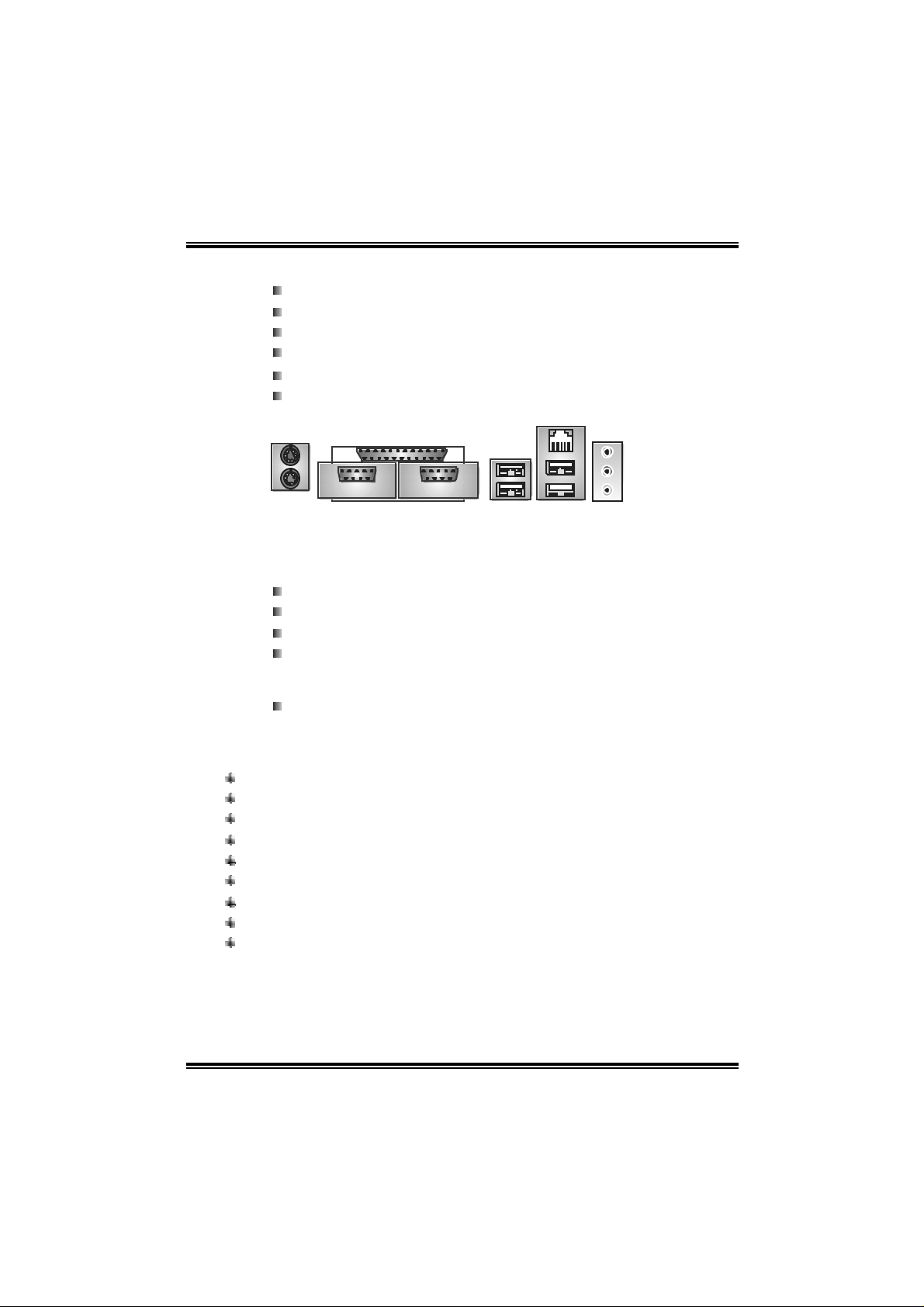
Rear (Back Panel) Side Connector s
1 PS/2 Mouse port and Key board port.
1 Printer Port.
1 Serial Port. (J C OM2 is optional.)
1 RJ -45 LAN jack.
4 USB 2.0 Ports.
3 audio port s support 6 channels audio-out fac ilities .
PS/2
Mouse
PS/2
Keyboard
COM1
Prin ter Port
COM 2
(optional)
B. BIOS & Software
BIOS
Award legal BIOS.
Supports APM1.2.
Supports ACPI.
Supports USB Func t ion.
USB *2
LAN
Connector
USB *2
Lin e- in/R ea r
Line-out
MI C- i n /
Center/
Left
Bundled So ftware
Supports 9th Touch™, WINFLASHER™ and F LASH ER ™.
1.2 PACKAGE CHECKLIST
FDD Cable X 1
HDD Cable X 1
Us er’s Manual X 1
Fully Setup D riv er CD X 1
Rear I/O Panel f or ATX C as e X 1
S/PD IF Cable X 1 (opt ional)
USB 2. 0 Cable X1 (opt ional)
Serial ATA Cable X 1(opt ional)
Serial ATA Power Swit c h C able X 1 (opt ional)
4
NF44X-A7
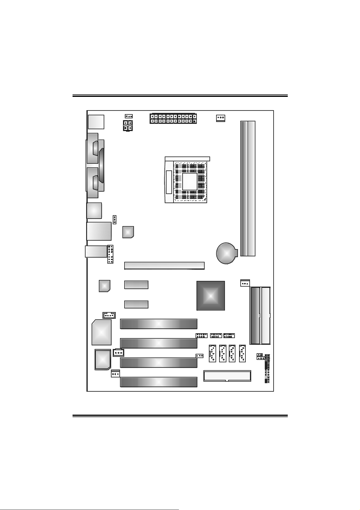
1.3 LA YOUT & COMPONENTS
JKBMS V1
JKBMS1
JCOM1
( o ptional )
JCOM2
JATXPWR2
JPRNT1
JATXPWR1
Socket 754
CPU1
JCFAN1
DIMM1
DIMM2
JUSB1
JUSBLAN1
JAU DI O1
Codec
JC DIN1
Super I/O
JUSBV1
LAN
JFAUD IO1
PEX1_1
PEX1_2
JSPDIF_OUT1
BIOS
JSFAN1
Note: ■ represents the 1
st
pin.
PCI1
PCI2
PCI3
PCI4
PEX16
nForce4 4X
JS ATA1
JUSBV2
BAT1
JNBFAN1
IDE2
IDE1
JUSB3 JUSB4JUSB2
JSAT A3
JCI1
JSATA2
FDD1
JSAT A4
JCMOS1
(optiona l )
JPANEL1
5
NF44X-A7
CHAPTER 2: HARDWARE I NSTALLATION
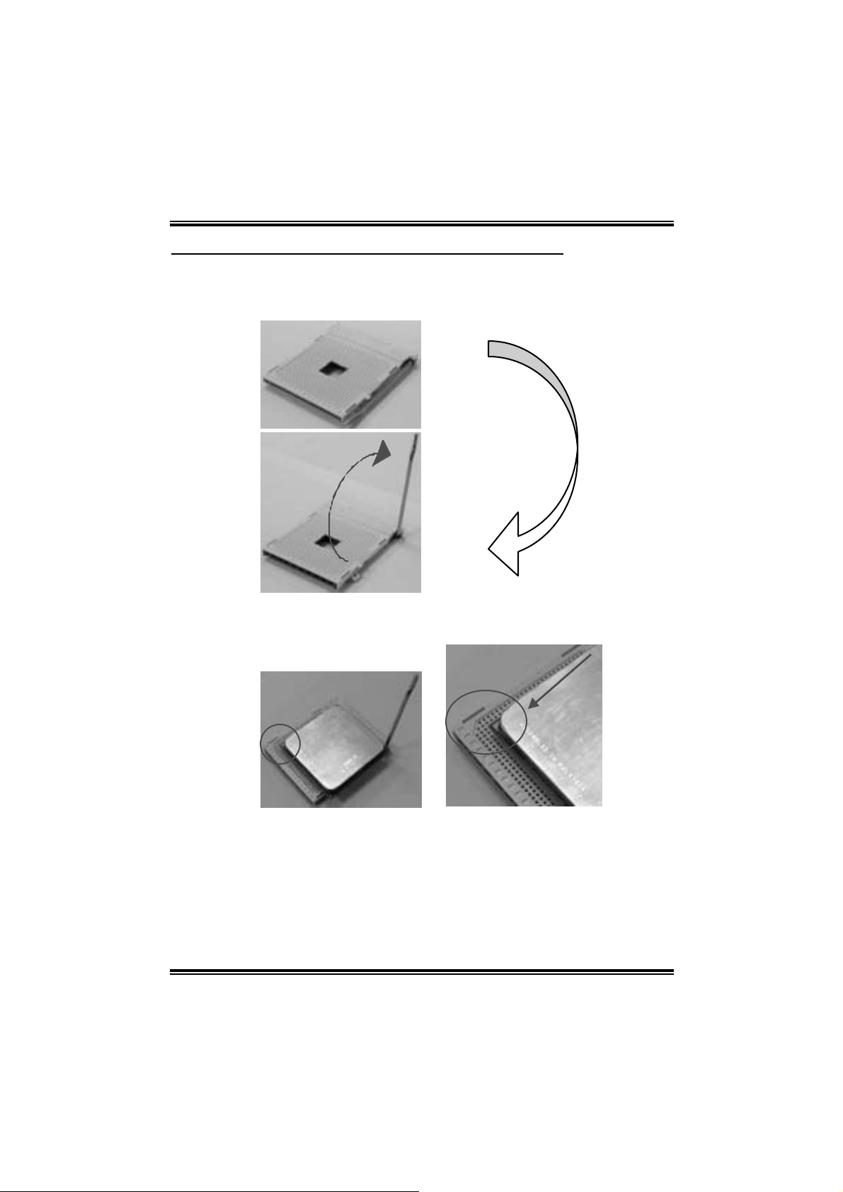
2.1 CENTRAL PROCESSING UNIT (CPU)
Step 1: Pull t he lev er s ideways away from t he socket and t hen raise t he lever up t o
Step 2: Look f or the black c ut edge on s ocket, and t he white dot on C PU should
a 90-degree angle.
point f orwards this blac k cut edge. The CPU will f it only in t he correct
orientation.
6
NF44X-A7
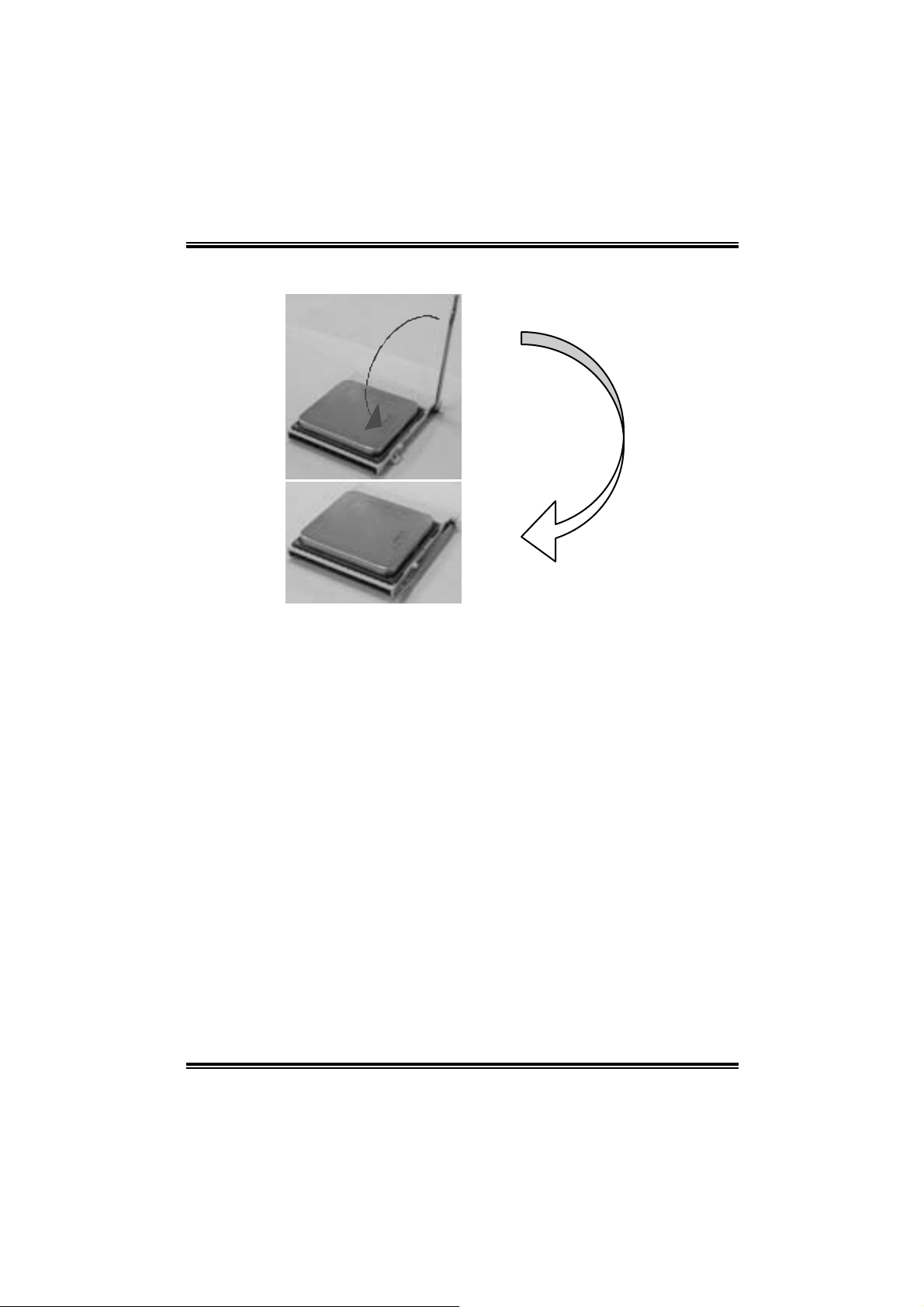
Step 3: Hold t he C PU down f irm ly, and then close t he lever t o c om plete t he
installation.
Step 4: Put t he CPU Fan on the CPU and buckle it. C onnect the C PU
cable to the JCFAN1. T his completes the installation.
FAN power
7
NF44X-A7
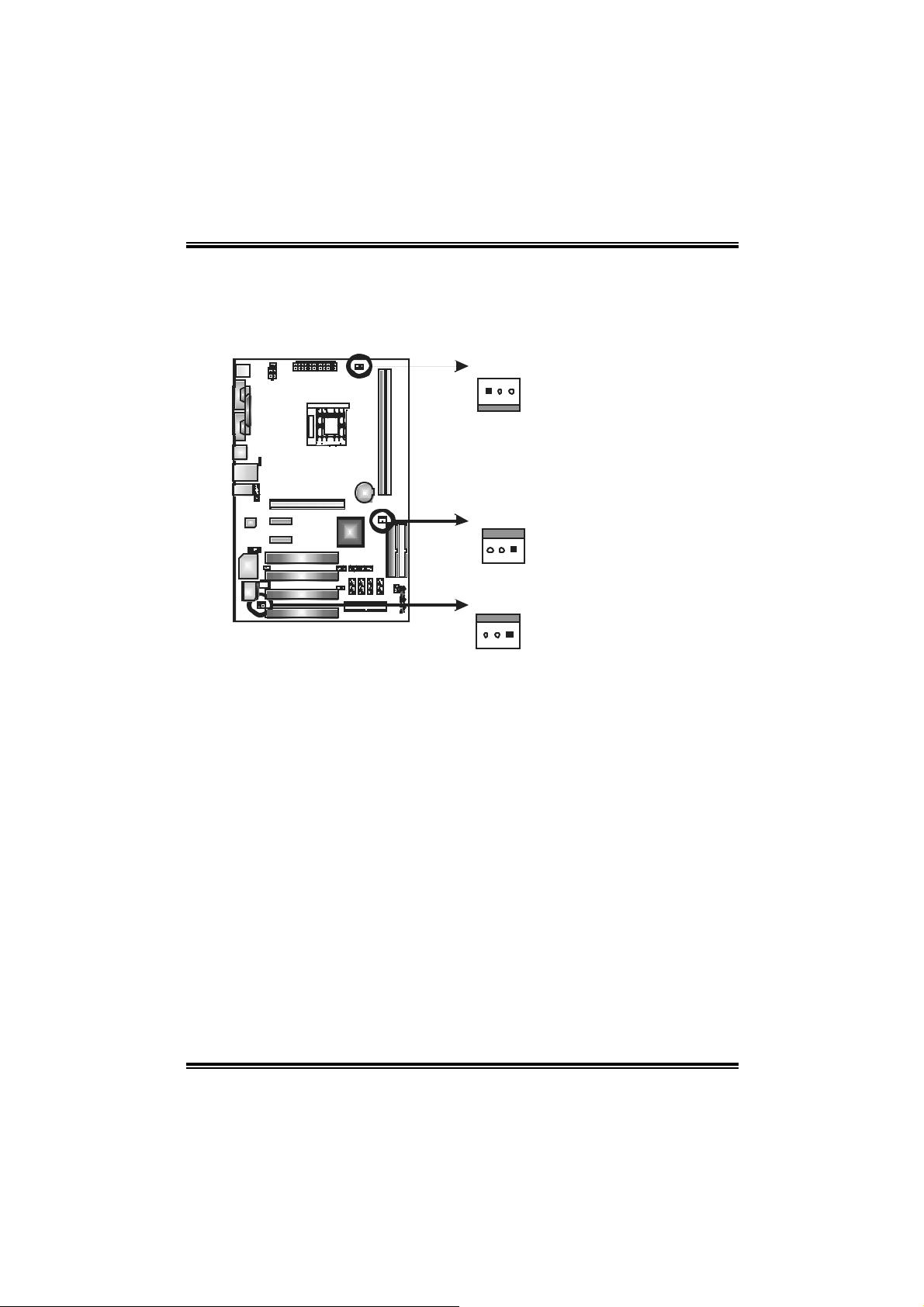
2.2 FAN HEADERS
CPU FAN Power Header : JCFAN1
S y s tem F a n P ow er H ea der: J SF AN 1
Nort h bridg e F an P o wer Hea der: J NBF AN 1
JCFAN1
13
JNBFAN1
13
JSFAN1
13
Note: The JCFAN1 and JSFAN1 support s ystem cooling fan with Smart Fan Control utility. It
supports 3 pin head c onnec tor. When connecting with wires onto c onnectors, pl ease note
that the red wire is the positive and should be connected to pin#2, and the black wire is
Ground and s hould be c onnected to GND.
Pin
Assignment
1 Ground
2 +12V
3 FAN RPM rate sense
(Only for JCFAN1 and
JSFAN1.)
8
NF44X-A7
2.3 MEMORY MODUL ES INS TAL LAT ION
DIMM1
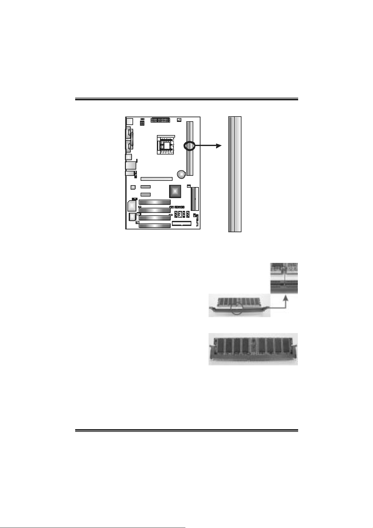
2.3.1 DDR Modu le ins tallat ion
1. U nloc k a DI MM slot by pres s ing t he ret aining clips outward. Align a DIMM on
the s lot s uc h t hat t he notch on t he DIMM mat c hes the break on t he Slot.
DIMM2
2. I ns ert the DIMM v ert ically and firmly into the s lot until the ret aining chip s nap
back in place and t he DIMM is properly seated.
9
NF44X-A7
2.4 CONNECTO RS & SLOTS
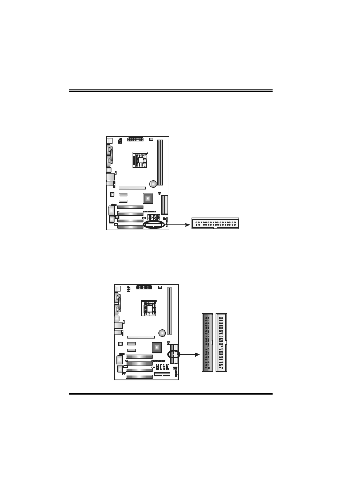
Floppy D isk Connector: FDD1
The motherboard provides a standard floppy disk c onnec t or that support s
360K, 720K, 1.2M, 1.44M and 2. 88M f loppy disk types. This connec t or
supports the prov ided f loppy drive ribbon cables.
2
1
34
33
Hard Disk Connectors: IDE 1/IDE2
The motherboard has t wo 32-bit Enhanced PC I IDE Cont roller that provides
PIO Mode 0~5, Bus Master, and Ultra DMA 33/ 66/100/133 func t ionality . It
has t wo H DD c onnectors IDE1 (prim ary ) and I D E2 (sec ondary ). The ID E
connec t ors c an c onnect a mas t er and a s lave driv e, so y ou can c onnec t up
to f our hard dis k drives . The f irst hard driv e should always be c onnected to
IDE1.
IDE2IDE1
3940
12
10
NF44X-A7
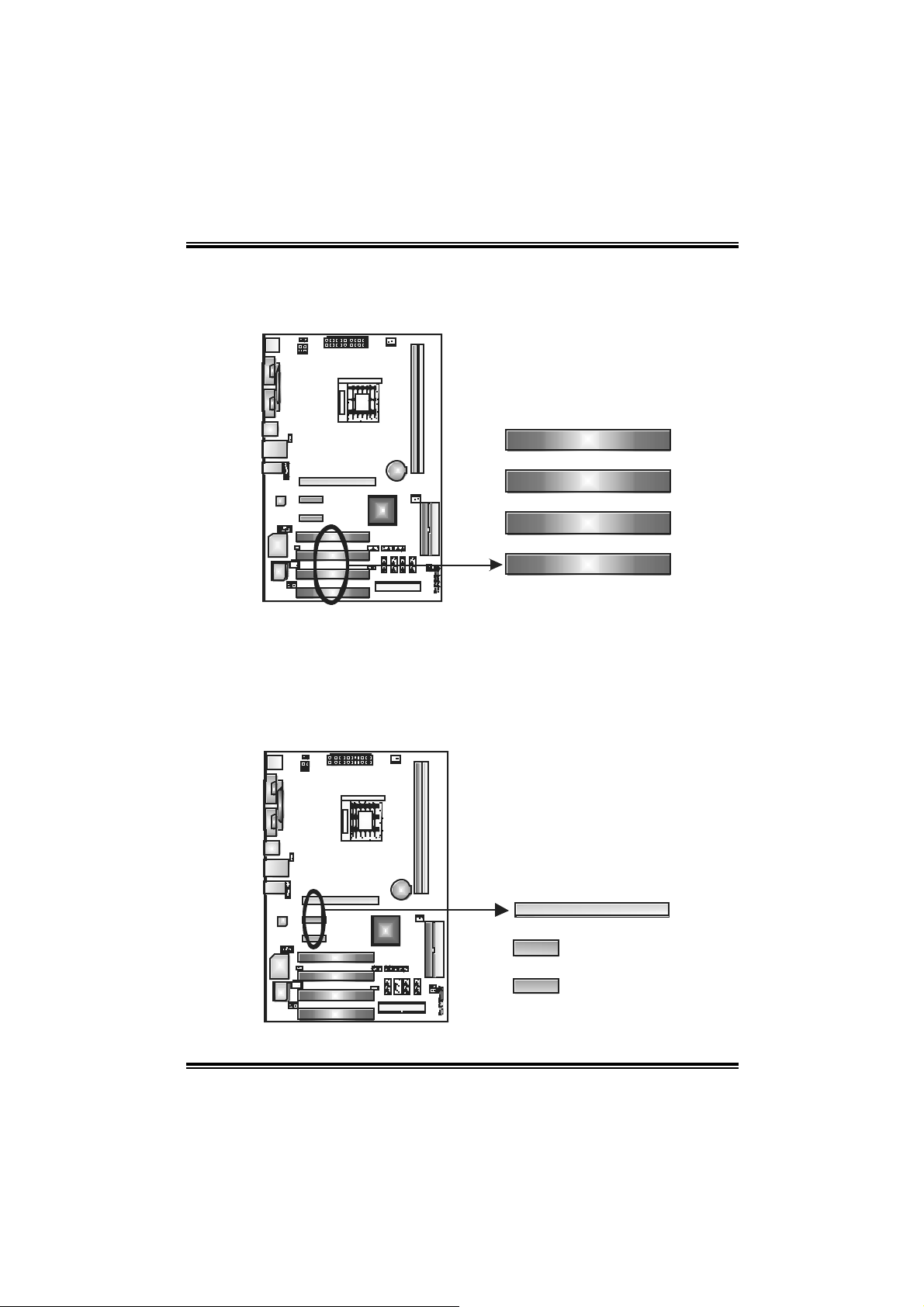
Perip heral Component Interconnect Slots: PCI1~PCI4
This mot herboard is equipped with 4 st andard PCI slot. PCI s t ands f or
Peripheral Com ponent I nt erc onnect, and it is a bus st andard for ex pans ion
cards . This PCI s lot is designat ed as 32 bits.
PCI1
PCI2
PCI3
PCI4
PCI-Express Slots: PEX16/ PEX1_1/PEX1_2
PEX1 6:
- PCI Express 1. 0a c om pliant.
- Maximum bandwidt h is up to 4GB/s per direction.
PEX1_1/PEX1_2:
- PCI Express 1. 0a c om pliant.
- Maximum bandwidt h is up to 250MB/s per direct ion.
11
PEX16
PEX1_1
PEX1_2
NF44X-A7
CHAPTER 3: HEADERS & JUMPERS SETUP
3.1 HOW TO SETUP JUMPERS
The illustrat ion shows how to s et up jum pers. When t he jum per cap is placed on
pins, the jum per is “close”, if not, that means the jum per is “open”.
Pin opened Pin closed Pin1-2 cl osed
3.2 DETAIL SETTINGS
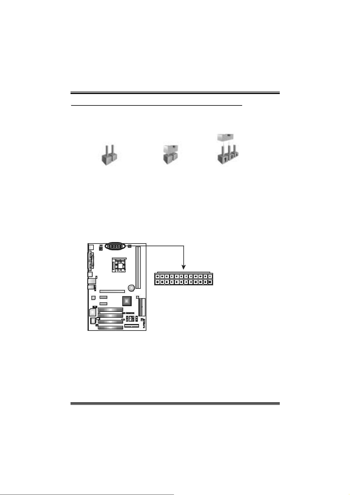
AT X Po wer Source Co nnector : JATX PWR1
This connector allows user t o c onnect 24-pin power connector on the ATX
power supply.
Pin Assignment
1 +3.3V
2 +3.3V
3 Ground
4 +5V
5 Ground
6 +5V
7 Ground
8 PW_OK
9 Standby
24 13
12
1
Voltage+5V
10 +12V
11 +12V
12 Detect
13 +3.3V
14 -12V
15 Ground
16 PS_ON
17 Ground
18 Ground
19 Ground
20 -5V
21 +5V
22 +5V
23 +5V
24 Ground
12
NF44X-A7
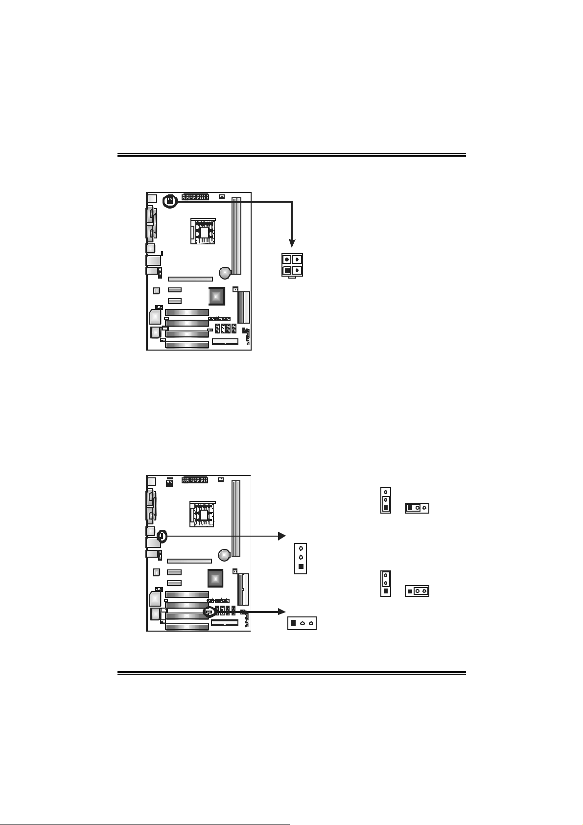
AT X Po wer Source Co nnector : JATX PWR2
By c onnecting this c onnector, it will prov ide +12V to CPU power circ uit.
Assignment
Pin
1 +12V
34
12
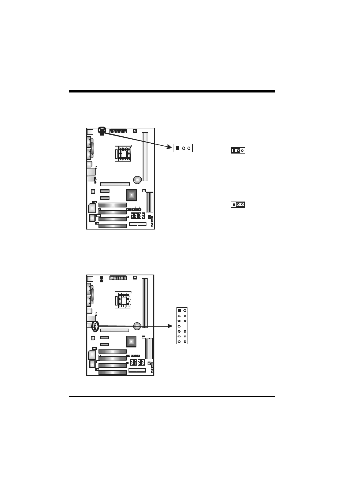
Power Source Headers fo r USB Ports: JUSBV 1/JUSBV 2
Pin 1-2 Cl o se:
JU SBV1: +5V for USB port s at JUSB1 and JU SBLAN 1.
JU SBV2: +5V for front USB headers (JU SB2/JU SB3/JUSB4).
Pin 2-3 Cl o se:
JU SBV1: U SB port s at JU SB1 and JUSBLAN 1 are powered with +5V standby
voltage.
JU SBV2: Front U SB headers (JUSB2/JUSB3/JUSB4) are powered with +5V
standb y voltage .
2 +12V
3 Ground
4 Ground
3
1
JUSBV1
Pin 1-2 Close
3
1
JUSB V2
3
1
Note: In order to support this functi on “Power-on s ystem via USB device,”
“JUSBV1/JUSBV2” jumper cap should be pl aced on Pin 2-3 i ndi viduall y.
13
3
1
Pin 2-3 Close
13
13
NF44X-A7
Power Source Header for PS/ 2 Keyboard/Mo use: JKB MSV 1
Pin 1-2 Cl o se: +5V for PS /2 keyboard and mouse .
Pin 2-3 Cl o se: PS/ 2 key board and mouse are powered with +5V standby
Note: In order to support this functi on “Power-on s ystem via keyboard and mouse”,
“JKBMSV1” jumper cap should be placed on Pin 2-3.
Front Panel Audio-out Header: JFAUDIO1
This connector will allow us er to c onnect with t he f ront audio out put headers on
the PC case. It will disable the out put on back panel audio c onnectors.
voltage.
13
1
3
Pin Assignment
1 MIC-in/
2 Ground
3 Stereo MIC-in L
4 Audio power
5 Right line-out/
2
1
6 Right line-out/
7 Reserved
8 Key
13
9 Left line-out/
14
10 Left line-out/
11 Right line-in (optional)
12 Right line-in (optional)
13 Left line-in (optional)
14 Left line-in (optional)
Pin 1-2 close
Pin 2-3 close
Stereo MIC-in R
Speaker-out Right.
Speaker-out Right
Speaker-out Left
Speaker-out Left
13
14
NF44X-A7
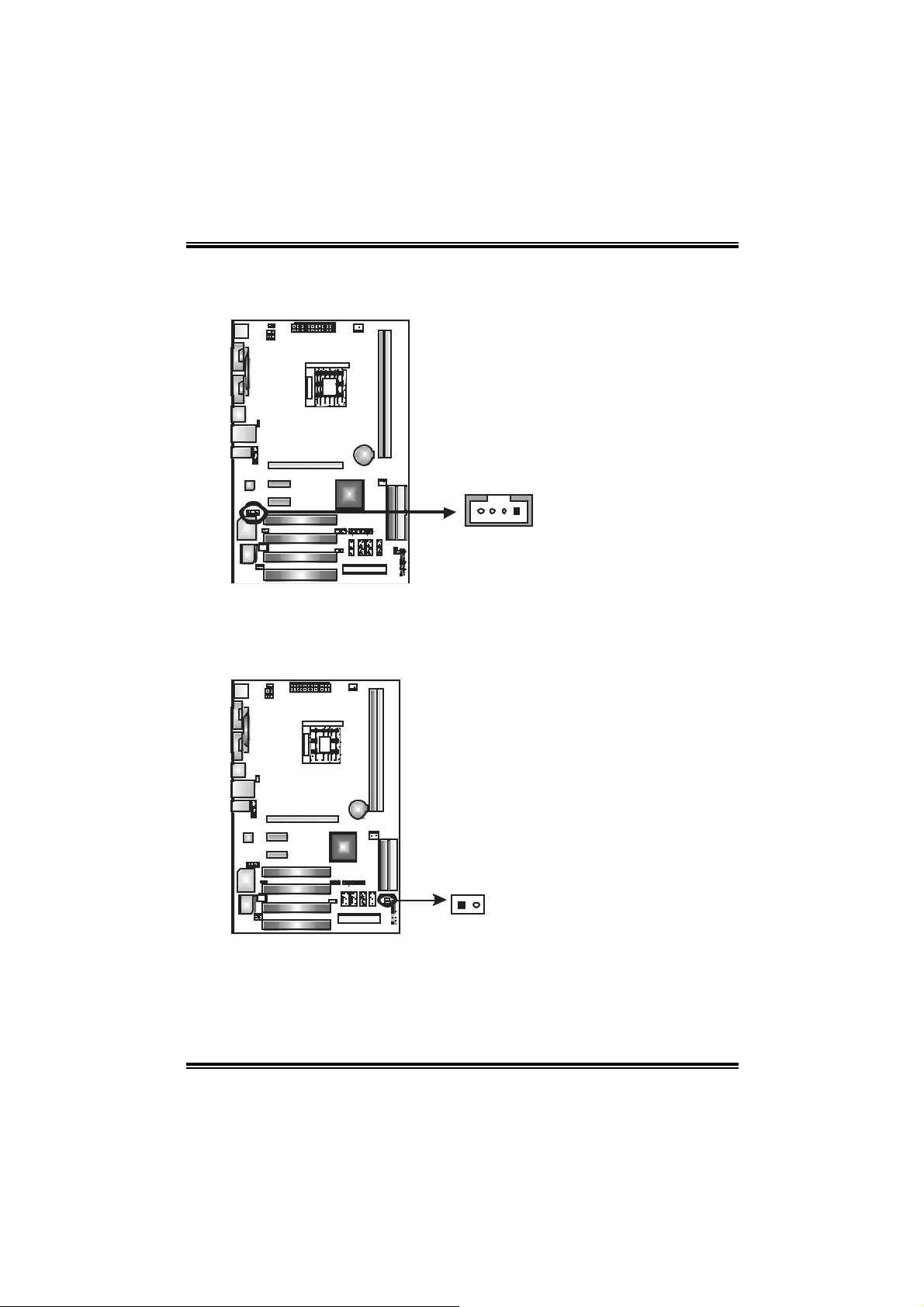
CD-ROM A u dio-in Co n ne cto r : J CDI N1
This connector allows us er to c onnect the audio s ourc e f rom the v ariety dev ices,
like CD-R OM, D VD -ROM, PC I sound card, PCI TV t urner card et c..
Assignment
Pin
1 Left channel input
2 Ground
3 Ground
4 Right channel input
14
Case Open Headers: J CI1
This connector allows sy stem to m onitor PC case open s t atus. If t he s ignal has
been triggered, it will rec ord t o the C MOS and show t he message on next
boot-up.
Assignment
Pin
1 Case open signal
2 Ground
JCI1
12
15
NF44X-A7
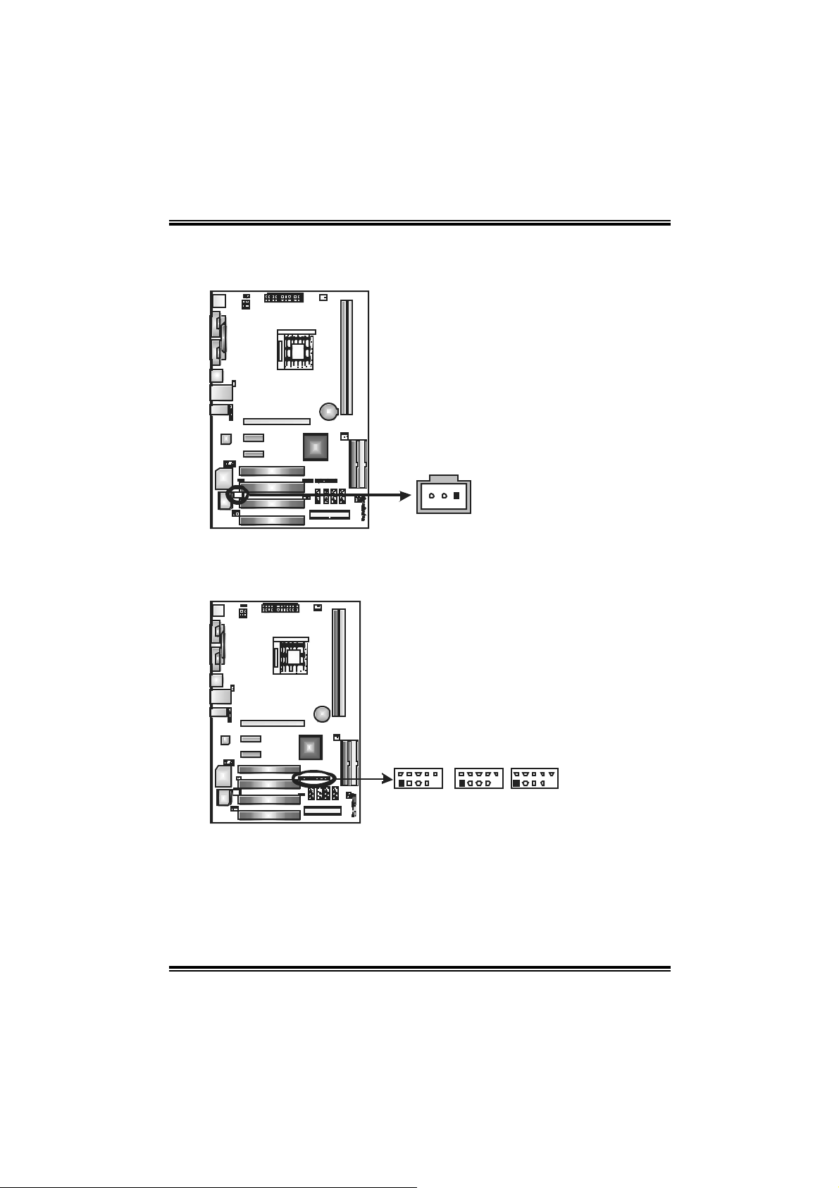
Dig ital A u dio-out C o n ne cto r : J SP DIF_ OU T 1
These connectors allow user t o c onnect the PCI bracket SPD IF out put or input
header.
Pin Assignment
1 +5V
2 SPDIF OUT
3 Ground
13
Headers fo r U SB Ports at F ro nt Panel: JUSB 2~JUSB4
This connector allows user t o c onnect additional U SB cables at PC f ront panel,
and also can be c onnec t ed wit h internal USB devices, like U SB card reader.
Pin
Assignment
1 +5V (fused)
2 +5V (fused)
3 USB4 USB5 USB+
6 USB+
7 Ground
8 Ground
210
19
JUSB4JUSB2
JUSB3
9 Key
10 NC
16
NF44X-A7
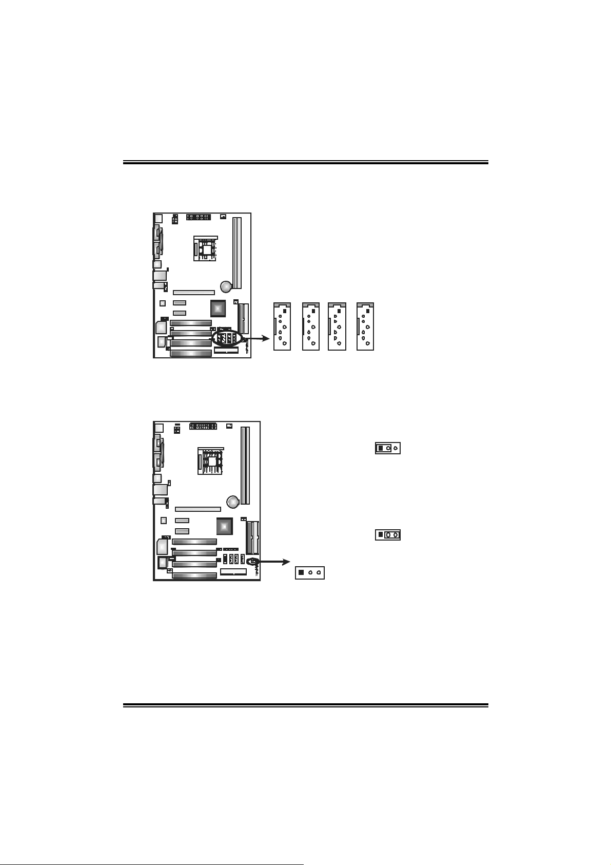
Serial ATA Connectors: JSATA1~JSAT A4
The motherboard has a SATA C ontroller in nForce4 4X SLI with 4 c hannels
SATA interf ac e, it satisfies the SATA 1.0 s pec and with t ransfer rate of 1.5Gb/s.
Assignment
Pin
1 Ground
2 TX+
3 TX-
JSAT A1
JSAT A2
JSAT A3
JSA TA4
JCMOS1: Clear CMOS Header
By plac ing the jum per on pin2-3, it allows user to rest ore the BI OS s af e set t ing
and the CMOS data, pleas e carefully follow the proc edures to avoid dam aging
the m otherboard.
4 Ground
5 RX-
1
6 RX+
7 Ground
4
7
13
Pin 1-2 close:
Normal Operation (Default).
3
1
Pin 2-3 close:
JCMOS1
31
Clear CMOS data.
Clear CMOS Procedures:※
1. R em ov e AC power line.
2. Set the jumper to “Pin 2-3 close”.
3. Wait for five seco n ds.
4. Set the jumper to “Pin 1-2 close”.
5. Power on the AC.
6. R es et your des ired pas s word or c lear t he CMOS dat a.
17
 Loading...