Biostar NF325-A7 Owner's Manual

NF325-A7
FCC Inf or m at ion and Copyright
This equipment h as been tested and f ound to comp ly with the limits of a Cl ass
B digi ta l dev i ce, pu r su ant to Part 15 of t he F CC Rul e s. Th e se lim its are de sig ned
to provide reasonable protection against harmful interference in a residential
installat ion. This equipment generates, use s and can radiate radio f requency
en ergy and, if not i nstalled and used in accor dance with the in structions, may
caus e harmful interfe rence to radio communications. There is no guarantee
that interference will not occur in a particular installation.
The vendor makes no representations or warranties with respec t to the
con te nt s h ere an d sp ec iall y di scl a im s an y imp li ed w arran t ies of mer c ha nt ab il ity
or fitness for any purpose. Furthe r the vendor reserves the right to revise this
publication and to make changes to the con tents here w ithout obligation t o
notify any party beforehand .
Duplication of this publication, in part or in whole, is not allowed without first
obt aining t h e vendor’s approval in writing.
The con te nt of thi s u ser’s m anu al is subje ct to b e ch ange d with ou t no tic e an d
we will not be responsible for any mistakes found in this user’ s manua l. All the
brand an d product names are trademarks of their r espect ive c ompanies.
i

TTaabbllee ooff CCoonntteennttss
Chapter 1: Introduction ...........................................................1
1.1 Mainboard Features...................................................... 1
1.2 Package Checklist......................................................... 4
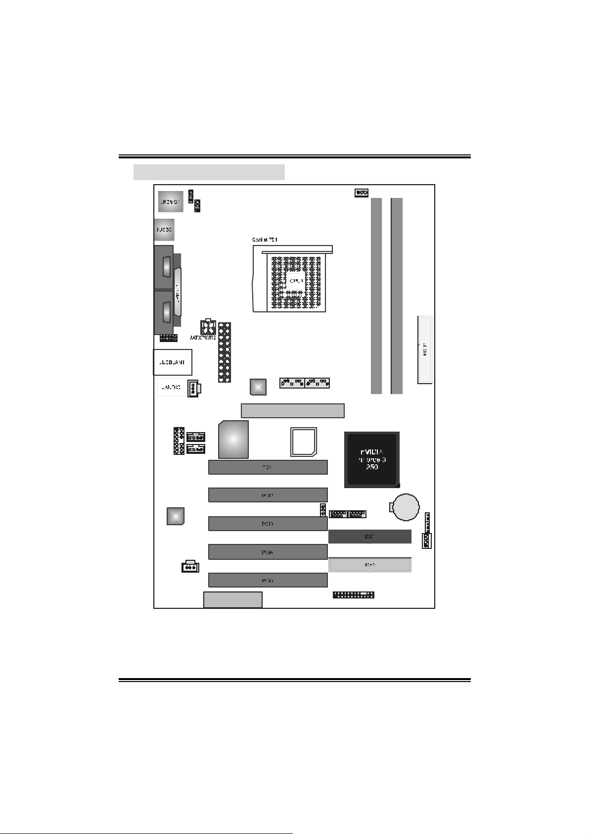
1.3 Layout of Version 1.0....................................................5
1.4 Components of Version 1.0........................................... 6
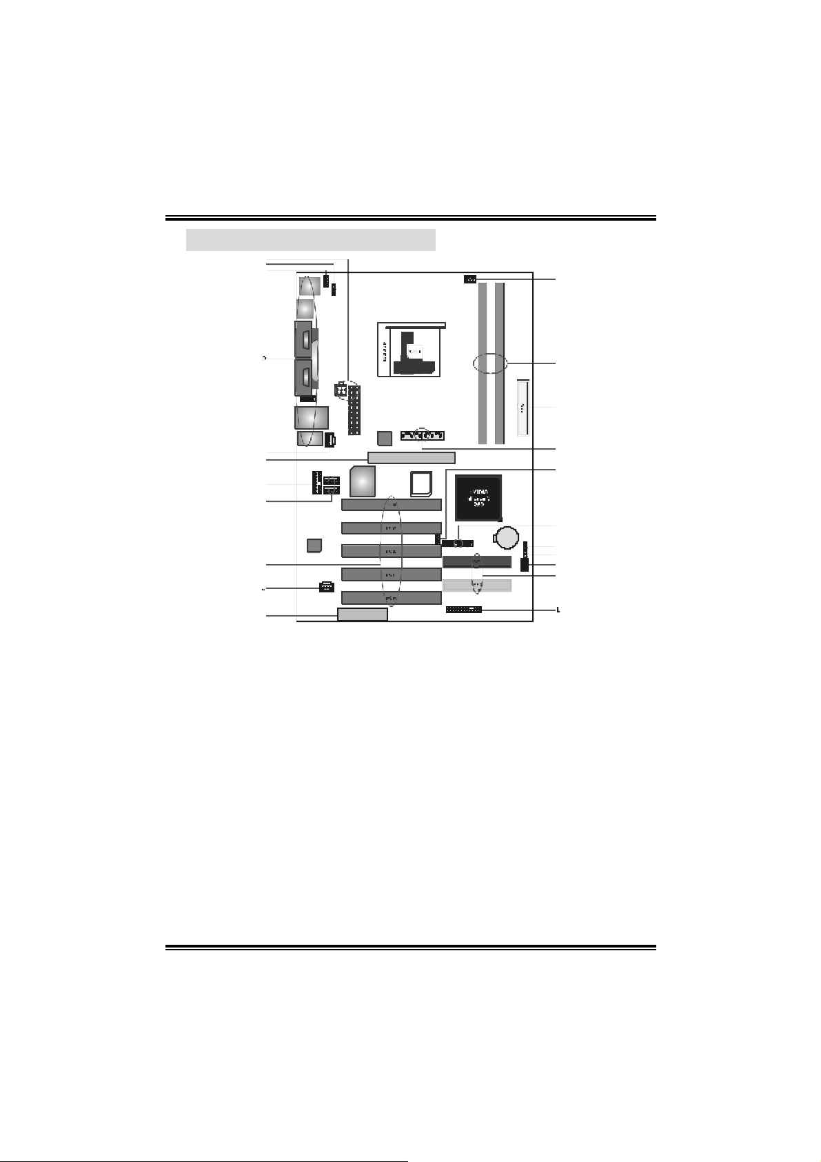
1.5 Layout of Version 1.1....................................................7
1.6 Components of Version 1.1........................................... 8
Chapter 2: Hardware Installation ..........................................9
2.1 Central Processing Unit (CPU)......................................9
2.2 Fan Headers................................................................11
2.3 Memory Modules Installation ......................................11
2.4 Connectors, & Slots.....................................................12
Chapter 3: Headers & Jumpers Setup...............................13
3.1 How to setup Jumpers .................................................13
3.2 Detail Settings.............................................................13
Chapter 4: Useful Help...........................................................18
4.1 Award BIOS Beep Code...............................................18
4.2 Extra Information........................................................18
4.3 Troubleshooting..........................................................20
Chapter 5: WarpSpeeder™...................................................21
5.1 Introduction................................................................21
5.2 System Requirement....................................................21
5.3 Installation ..................................................................22
5.4 [WarpSpeeder™] includes 1 tray icon and 5 panels........23
ii

NF325-A7
CHAPTER 1: INTRODUCTION
1.1 MAINBOAR D FEATURES
A. Hardware
CPU
Supports Socket 754.
Sup por ts AMD At h l on 64 / Sem pr on pr oc ess or.
Chi pset
NVIDIA nForce3 250.
- HyperT ransport link to the AMD Athlon 64 CPU.
- Sup por ts AGP 3.0 8x in ter face.
- Supports sy stem and power management.
- Supports PIO Mode 5, Bride Mode and Ultra DMA
33/ 66/10 0/1 33 Bus Mas ter Mod e.
- Supports USB 2.0, 8 ports.
- Complaints with PCI Versi on 2.3 specificati on.
- Complaints with AC’97 Versi on 2.3 specification.
- Fast ATA/133 IDE controllers.
Dimensions
ATX Form Fac tor:
2 0.5 cm (W) * 29.3cm (L) (Version 1. 0)
20.5cm (W) * 30.48cm (L) (Versi on 1.1)
Slots
Five 32-bit PCI bus master slots.
One AGP 8x s lot
One CNR slot, f or Ve rsi on 1.1 only.
(See p.12 for supporting informati on.).
Se rial ATA
Supports 2 serial ATA (SATA) ports.
Compliant with SATA 1.0 specifi cation.
Data tran sfer rates up to 150MB /s
1
NF325-A7
Ma in Me mory
Supp ort s up to 2 DDR d evi ces.
Supp ort s 200 /266/333/400 MHz DDR de v ices.
Certified DDR400 List
- Please check the website:
http://www.biostar.com.tw/products/mainboard/board.php3?
name=NF325-A7
Maxi mu m memor y size is 2GB.
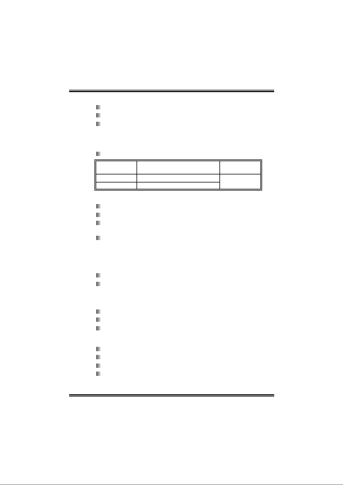
DI MM Socket
Location
DIMM1 128MB/256MB/512MB/1GB *1
DIMM2 128MB/256MB/512MB/1GB *1
DDR Module
To t a l M e m o r y
Size (MB)
Max is 2 GB.
Super I/O
Chip: ITE IT8712F.
Low Pin Count Interface.
Provides the most commonly used legacy Super I/O
functionality.
Environment Control initiatives,
- H/W Monitor
- IT E's "Smart Guardi an" fu n ction
On Board IDE
Supports 4 IDE disk drives.
Supports PIO mode 4, Bl ock Mode and Ultra DMA
33/ 66/10 0/1 33 bus master mo de.
10/100 LAN
PHY: RTL8201BL
Supports 10 Mb/s and 100 Mb/s auto-negotiation.
Half/Full duplex capability.
On Board AC’97 Sound Cod ec
Chip: ALC655
Compliant with AC’97 Versi on 2.3 specification.
Supports S/PDIF-out (optional).
Supports 6 channels.
2
NF325-A7
F ront Sid e On-board P eripheral s
1 audio out header supports 1 line-in, 1 line-out, and 1MIC
ports.
1 serial header supports 1 seri al COM port. (JCOM2, optional )
1 CD-i n connector supports 1 CD-ROM device.
(One extra CD-in connector is optional for v1.1 only.)
1 S/PDIF-out connector supports 1 di gital audio-out port.
(Digital audio-out function i s opti onal for both versi ons.).
1 S/PDIF-in connector supports 1 digital audi o-in port.
(Digital audio-in function i s opti onal for v1.1 only.)
1 floppy connector supports 2 FDD devices with 360K, 720K,
1.2 M, 1.44M and 2.88Mby tes.
2 USB headers support 4 USB 2.0 ports.
2 IDE connectors support 4 hard disk devices.
2 Serial ATA connectors support 2 SATA devices.
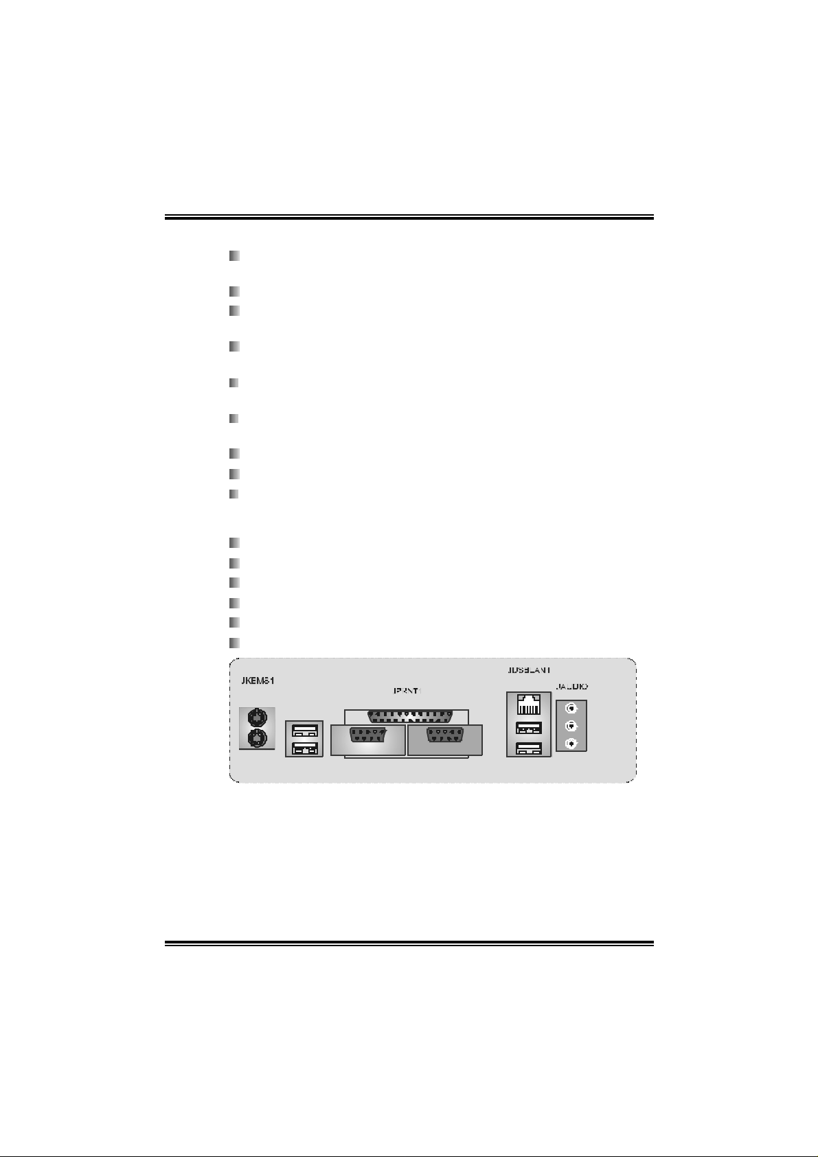
Re ar (Bac k) Side Co n n ect or s
1 par allel por t.
1RJ-45 LAN jack.
1 audio port.
1 PS/2 keyboard & mouse port.
1 serial port. (JCOM3 is optional.)
4 USB 2.0 ports.
PS/2
Mouse
PS/2
Keyboard
USB x2
COM1
Parallel
3
COM3
(optional)
LAN
USB x2
Line In/
Surround
Line Out
Mic In 1 /
Base/Cente r

NF325-A7
B. BIOS & Software
BIOS
Award legal BIOS.
Supports APM1.2.
Supports ACPI.
Suppo rts USB Functi on.
Software
Sup por ts War pspeeder ™ , 9th To uc h™, W IN F LASH ER ™ and
FLASHER™.
Offers the hi ghest performance for Windows 9 8 SE, Windows
2000, Windows Me, Windows XP, SCO UNIX etc.
1.2 PACKAGE CHECKLIST
FDD Cable X 1
HDD Cable X 1
User’s Manu al X 1
Fu lly Setup Driver CD X 1
Rear I/O Panel fo r ATX Case X 1
USB 2.0 Cable X1 (optional)
S/PDIF Cable X 1 (optional )
Serial ATA Cable X 1 (optional)
Serial ATA Power Switch Cable X 1 (optional )
4
NF325-A7
A
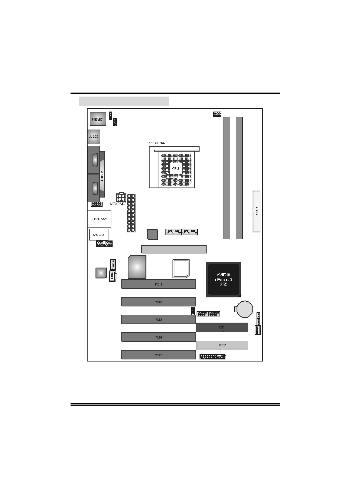
1.3 LAYOUT OF VERSION 1.0
JKBMSV1
1
JUSBV1
1
1
JCFAN1
DDR1
DDR2
JCOM 3* JCOM1
1
JCOM 2*
1JAUDIO1
Codec
1
JSP DIF _ OUT
JCDIN1
1
JATXPWR1
Super I/O
LAN
JSAT A517JSATA4
17
GP1
BIOS
1
JUSBV3
JUSB2
1
2
1
JPANEL1
JUSB1
1
BAT1
JCI1
1
JCMOS1
1
1
JSFAN1
24
23
Note:
1. ● represents the 1st pin.
2. JCOM2 and JCOM3 are optional, and onl y one of them can be chosen.
5
NF325-A7
A
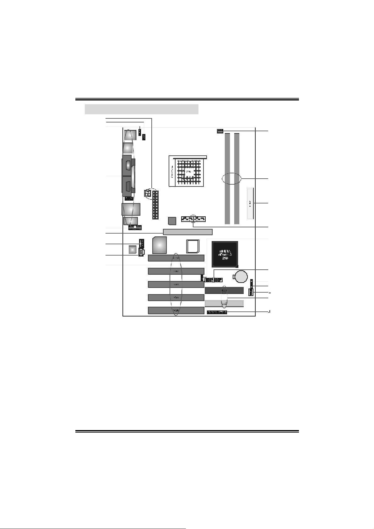
1.4 COMPONENTS OF VERSION 1.0
A
B
C
T
D
E
F
G
H
I
JATXPW R 1~2: ATX power
A.
Codec
Super I/O
connectors.
JU SBV1: Power sourc e f or JUSB3.
B.
JKBMSV1: Power source for JKBMS1.
C.
Back panel connectors.
D.
JAU DIO1: Audio out header.
E.
AGP1: Accelerated Graphic s Port s lot.
F
JCDIN1: CD-ROM audio-in header
G.
JSPD IF_OU T: Digit al audio out header
H.
(optional).
PCI 1~5: Peripheral Com ponent
I.
Int erc onnect slots.
JPANEL1: Front panel c onnector.
J.
DDR1
DDR2
LAN
GP1
BIOS
BAT 1
S
R
Q
P
O
N
M
K
ID E1~2: Hard disk connectors.
K.
JSFA N1: S yste m fan connector.
L.
JCMOS1: Clear CMOS Heade r.
M.
JCI1 : Case open Header.
N.
JU SB1~2: Front USB headers .
O.
JUSBV3: Power source for JUSB1~2.
P.
JSATA4~5: Serial ATA c onnec t ors.
Q.
FDD1: Flopp y disk connector .
R.
DDR1~2: DDR memor y modules.
S.
JCFAN1 : CPU fan connector
T.
6
NF325-A7
A
1.5 LAYOUT OF VERSION 1.1
JKBMSV1
1
JUSBV1
1
1
JCFAN1
DDR1
DDR2
JCOM3* JC OM1
1
JC OM2*
1
JAU DIO11J CDIN1
Codec
JSPDIF_OUT
JSPDIF_IN
(optional)
JC DIN2
(o pti o na l)
(optional)
1
1
JATXPWR1
JSATA517JSATA4
LAN
1
Super I/O
CNR
GP1
BIOS
17
JUSBV3
1
1
2
1
JUSB2
JUSB1
1
JPANEL1
BAT1
JC I1
1
JCMOS1
1
1
JSFAN1
24
23
Note:
1. ● represents the 1st pin.
2. JCOM2 and JCOM3 are optional, and onl y one of them can be chosen.
7
NF325-A7
V
A
1.6 COMPONENTS OF VERSION 1.1
A
B
C
E
F
G
H
Codec
I
K
JATXPW R 1~2: ATX power
A.
connectors.
JU SBV1: Power sourc e f or JUSB3.
B.
JKBMSV1: Power source for JKBMS1.
C.
Back panel connectors (including
D.
COM2 header).
JSPD IF_IN: Digital audio out header
E.
(optional).
AGP1: Accelerated Graphic s Port s lot.
F
JAU DIO1: Audio out header.
G.
JCDIN1/JCDIN2 : CD- ROM audio-in
H.
header. (JCDIN2 is opt ional. )
PCI 1~5: Peripheral Com ponent
I.
Int erc onnect slots.
JSPD IF_OU T: Digit al audio out header
J.
(optional).
K. CNR1:
Communi cation Network
R i ser sl ot.
Super I/O
CNR
D DR1
DDR 2
LA N
GP1
BIOS
BAT1
U
T
S
R
Q
P
O
N
M
JPANEL1: Front panel c onnector.
L.
ID E1~2: Hard disk connectors.
M.
JSFA N1: S yste m fan connector.
N.
JCMOS1: Clear CMOS Heade r.
O.
JCI1 : Case open Header.
P.
JU SB1~2: Front USB headers .
Q.
JUSBV3: Power source for JUSB1~2.
R.
JSATA4~5: Serial ATA c onnec t ors.
S.
FDD1: Flopp y disk connector .
T.
DDR1~2: DDR memor y modules.
U.
JCFAN1 : CPU fan connector
V.
8
NF325-A7
CHAPTER 2: HARDWARE INSTALLATION
2.1 CENTRAL PROCESSING UNIT (CPU)
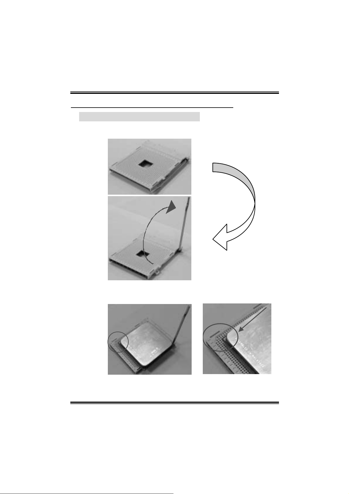
Step 1: Pull the lever sideways away from the socket and then raise the
lever up to a 90-degree angl e.
Step 2: Look for the bl ack cut edge on socket, and the white dot on CPU
should point forwards this bl ack cut edge. T he CPU wi ll fit onl y in
the correct orientati on.
9
NF325-A7
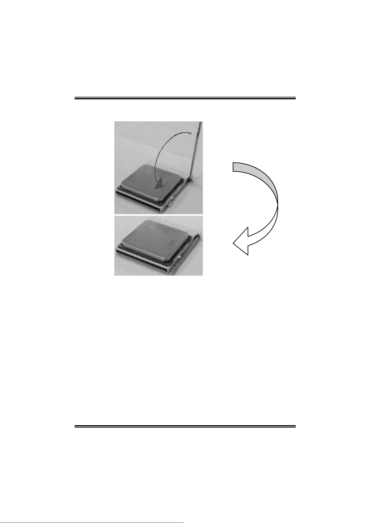
Step 3: Hold the CPU down firml y, and then close the lever to complete
the i nstalla ti on.
Step 4: Put the CPU Fan on the CPU and buckle it. Connect the CPU FAN
power cable to the JCFAN1. This completes the i nstallation.
10
NF325-A7
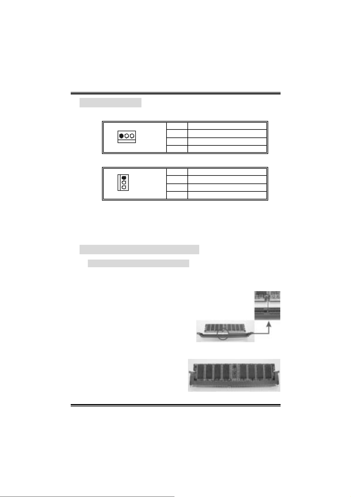
2.2 FAN HEADERS
CPU FAN Hea der: JCFAN1
Pin Assignment
1
JCFAN1
1 Ground
2 +12V
3 FAN RPM rat e s ens e
System Fan H eader: JSFAN1
1
JSFAN1
Note:
The JCF AN1 and J SF AN 1support sy stem cooling fan with Smart Fan
Cont rol utility. I t supports 3 pin head c onnector. When connec t ing with wires
onto c onnectors, please not e t hat t he red wire is the pos itive and should be
connec t ed to pin#2, and the black wire is Ground and should be c onnected
to GND.
Pin Assignment
1 Ground
2 +12V
3 FAN RPM rat e s ens e
2.3 MEMORY MODULES INSTAL LAT ION
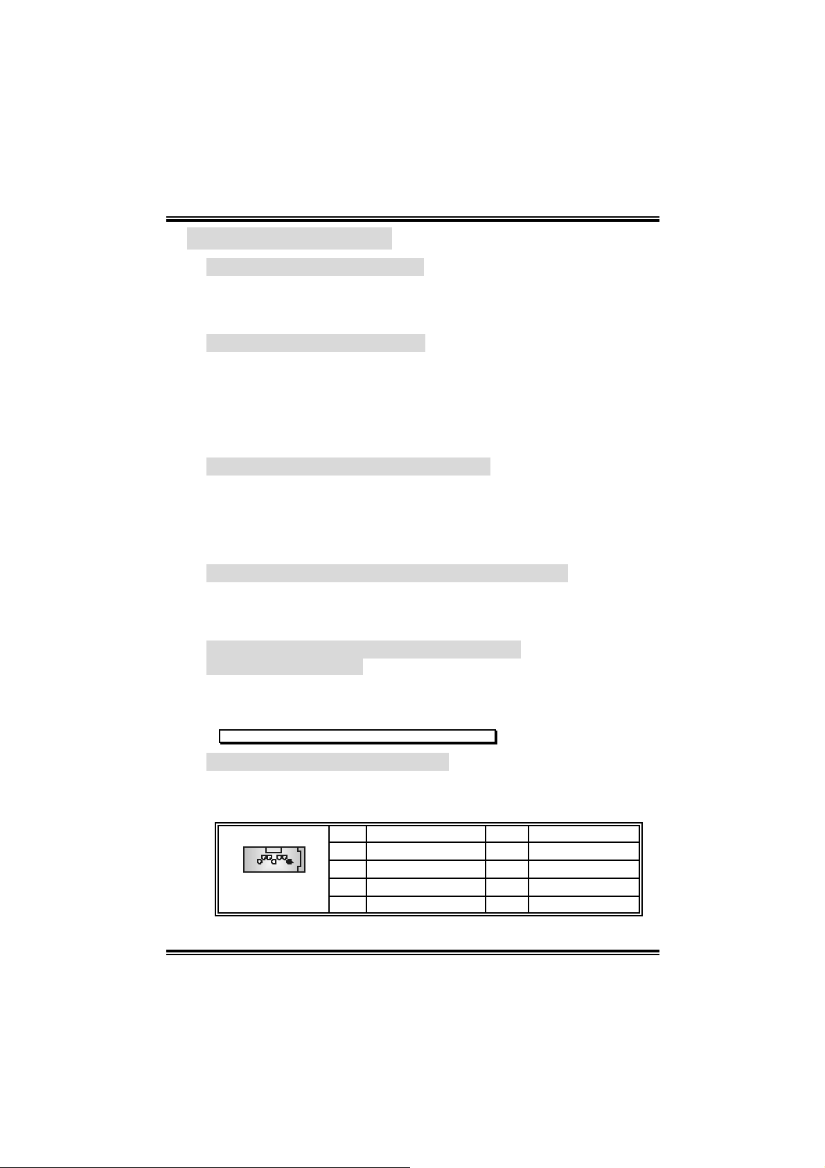
2.2.1 DDR Modu le ins tallation
1. Unlock a DIMM sl ot by pressing the retaining clips outward. Align a
DIMM on the slot such that the notch on the DIMM m atches the break
on the Sl ot.
2. Insert the DIM M vertically and firmly into the sl o t until the retain ing chip
snap back in place and the DIMM i s properl y seated.
11
NF325-A7
2.4 CONNECTO RS, & SLOTS
Floppy D isk Connector: FDD1
The m otherboard provides a standard floppy di sk connector that
s uppor t s 360 K, 720K, 1.2 M, 1.44M and 2.88M flo ppy d isk types. This
connector supports the provided floppy drive ri bbon cables.
Hard Disk Connectors: IDE1~2
The m otherboard has a 32-bit Enhanced PCI IDE Control ler that
provides PIO Mode 0~5, Bus Master, and Ultra DM A 33/66/100/133
functionalit y. It ha s two HDD connec tors IDE 1 (prima ry ) an d IDE2
(secondary). The IDE connectors can connect a master and a slave
dri ve, so you can connect up to four hard disk drives. The first hard drive
should always be connected to IDE1.
AGP1: Accelerated Graphics Port Slot
You r mon ito r will atta c h directly to that vide o card. Thi s m otherbo ard
supports video cards for PCI sl ots, but it i s al so equi pped with an
Accelerated Graphi cs Port (AGP). An AGP card will take advantage of
AGP technol ogy for improved vi deo effi ci ency and performance,
especially with 3D graphi cs.
Peripheral Component Interconnect Slots: PCI1~5
This motherboard is equi pped with 1 standard PCI sl ot. PCI stands for
Peripheral Component Interconnect, and it is a bus standard for
expansi on cards. This PCI slot i s designated as 32 bits.
CNR1: Communication Network Riser Slot
(For Version 1.1 only)
The CNR specificati on is an open I nd ustry Standar d Ar c hi tecture, an d it
defines a hardware scalabl e riser card i nterface, whi ch supports modem
only.
Note: This CNR slot supports Smartlink CNR Card only.
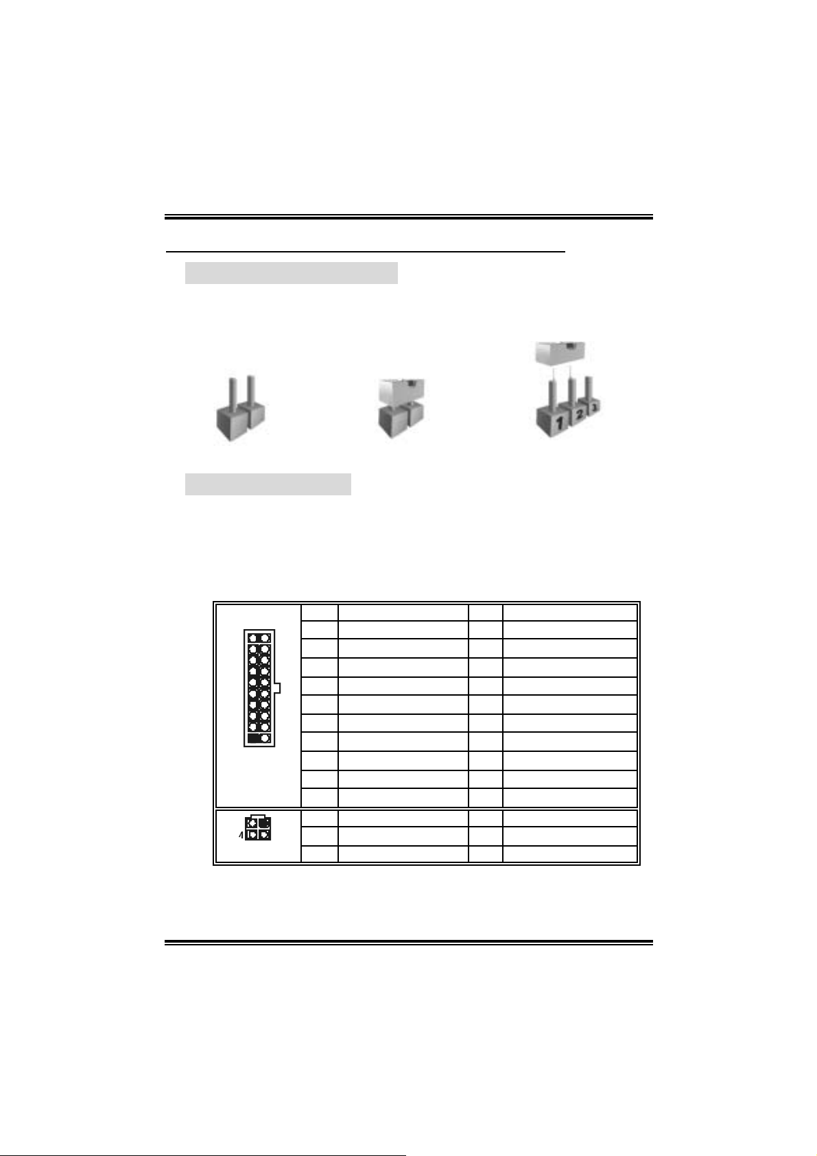
Serial ATA Connect or: JSATA4~5
The m otherboard has a SATA Controller in nForce 3 250 with 2 channels
SATA interface; it satisfies the SATA 1.0 spec and with transfer rate of
1.5Gb/s.
Pin Assignment Pin Assignment
1 Ground 2 TX+
7
JSATA4/JSATA5
1
3 TX- 4 Ground
5 RX- 6 RX+
7 Ground
12
NF325-A7
CHAPTER 3: HEADERS & JUMPERS SETUP
3.1 HOW TO SETUP JUMP ERS
The illustration shows how to set up jumpers. When the j umper cap is
placed on pins, the jumper is “cl ose”, if not, that means the jumper is
“open”.
Pin opened Pin closed Pin1-2 closed
3.2 DETAIL SETTINGS
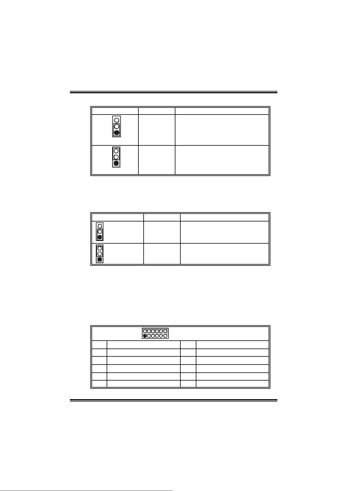
Pow er Con nector s: JATX PWR1/PATXPWR2
JATXPWR1: Thi s connector allows user to connect 20-pin power
conn ec tor on t h e A TX power s upp ly.
JATXPWR2: By connecting thi s connector, it will provide +12 V to CPU
power ci rcuit.
10
1
JATXPWR1
JATXPWR2
20
11
12
3
Pin Assignment Pin Assignment
1 +3.3V 11 +3.3V
2 +3.3V 12 -12V
3 Ground 13 Ground
4 +5V 14 PS_ON
5 Ground 15 Ground
6 +5V 16 Ground
7 Ground 17 Ground
8 PW_OK 18 -5V
9 Standby Voltage +5V 19 +5V
10 +12V 20 +5V
Pin Assignment Pin Assignment
1 +12V 3 Ground
2 +12v 4 Ground
13
NF325-A7
Powe r Sou rce Selection He ade rs for US B: JUSBV1/JUSBV3
Assignment Description
3
1
+5V
JUSBV1: +5V for JUSB3.
JUSBV3: +5V for JUSB1/2.
Pin 1-2 clo se
3
1
Pin 2-3 clo se
+5V st andby
Voltage
JU SBV1: JUSB3 is powered wit h +5V
standb y voltage.
JU SBV3: JUSB1/2 are powered +5V
standb y voltage.
Note:
In order to support thi s function “Power-on system via USB device,”
“J U SBV3” ju mp er cap s hou ld be p lace d on Pin 2-3 indiv id ua l ly .
Power S o urce Se lectio n H ead er s for K eyb o ar d /Mous e: JKBMSV1
Assignment Description
3
1
Pin 1-2 close
3
1
Pin 2-3 close
Note:
In order to support thi s function “Power-on system via keyboard and
mouse”, “JKBMSV1” j umper cap shoul d be placed on Pin 2-3.
+5V +5V for PS /2 keyboard and mouse
+5V Standby
Voltage
PS/2 k eyboard and m ous e are
powered wit h +5V standby v oltage.
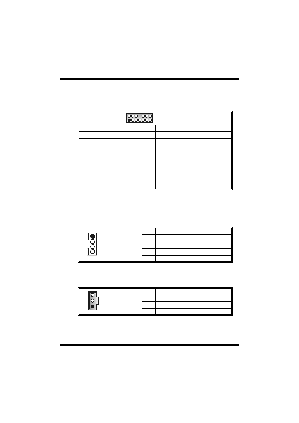
COM2 Heade r: JCOM2 (Optional)
This header allows user to connect additional serial cable on the PC
back panel. It can be used to connect serial devices, for example,
mouse or modem.
2
1
Pin Assignment Pin Assignment
1 RIN1 2 RIN3
3 DOUT2 4 DOUT3
5 Ground 6 RIN2
7 DOUT1 8 RIN4
9 -XRI1 10 NA
10
9
JCOM2-Header
14
NF325-A7
Front Panel Audio - out Header: JAUDIO1
This conn ecto r will allow user t o c on nect with the front audio ou t put
head ers on the PC c ase. It will d isable the ou tp ut on bac k pan el audio
connectors.
2
1
Pin Assignment Pin Assignment
1 Mic in/center 2 Ground
3 Mic power/Bas s 4 Audio power
Right line out/ Speak er out
5
Right
7 Reserv ed 8 Key
9 Lef t line out /Speaker out Left 10 Lef t line out /Speaker out Left
Right line in/R ear s peak er
11
Right
13 Left line in/R ear speak er Lef t 14 Lef t line in/ R ear s peaker Lef t
14
13
JAUDIO1
Right line out/ Speak er out
6
Right
Right line in/R ear s peak er
12
Right
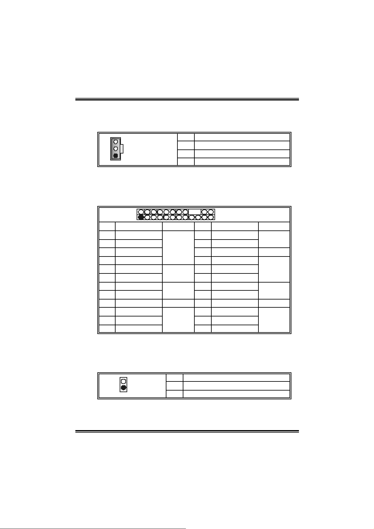
CD-ROM Audio-in Connector: JCDIN1/JCDIN2
(J CDI N 2 is op t i on a l.)
This connector allows user to connect the audio source from the variety
devi c es, like CD-ROM, DVD-ROM, PCI soun d card, PCI T V turner card
etc..
Pin Assignment
1
JCDIN1/JCDIN2
1 Left channel input
2 Ground
3 Ground
4 Right channel input
Digital Audio-out Connector: JSPDIF_OUT (optional)
This conn ecto r will allow user t o c on nect th e P CI bracket SP DIF ou tput
header.
Pin Assignment
1 +5V
1
JSPDIF_OUT
2 SPDIF OUT
3 Ground
15
NF325-A7
Digita l Aud io-i n Connector: JSPDIF _IN (op tio nal)
This conn ecto r will allow user t o c on nect th e P CI bracket SP DIF ou tput
header.
Pin Assignment
1 +5V
1
JSPDIF_OUT
2 SPDIF OUT
3 Ground
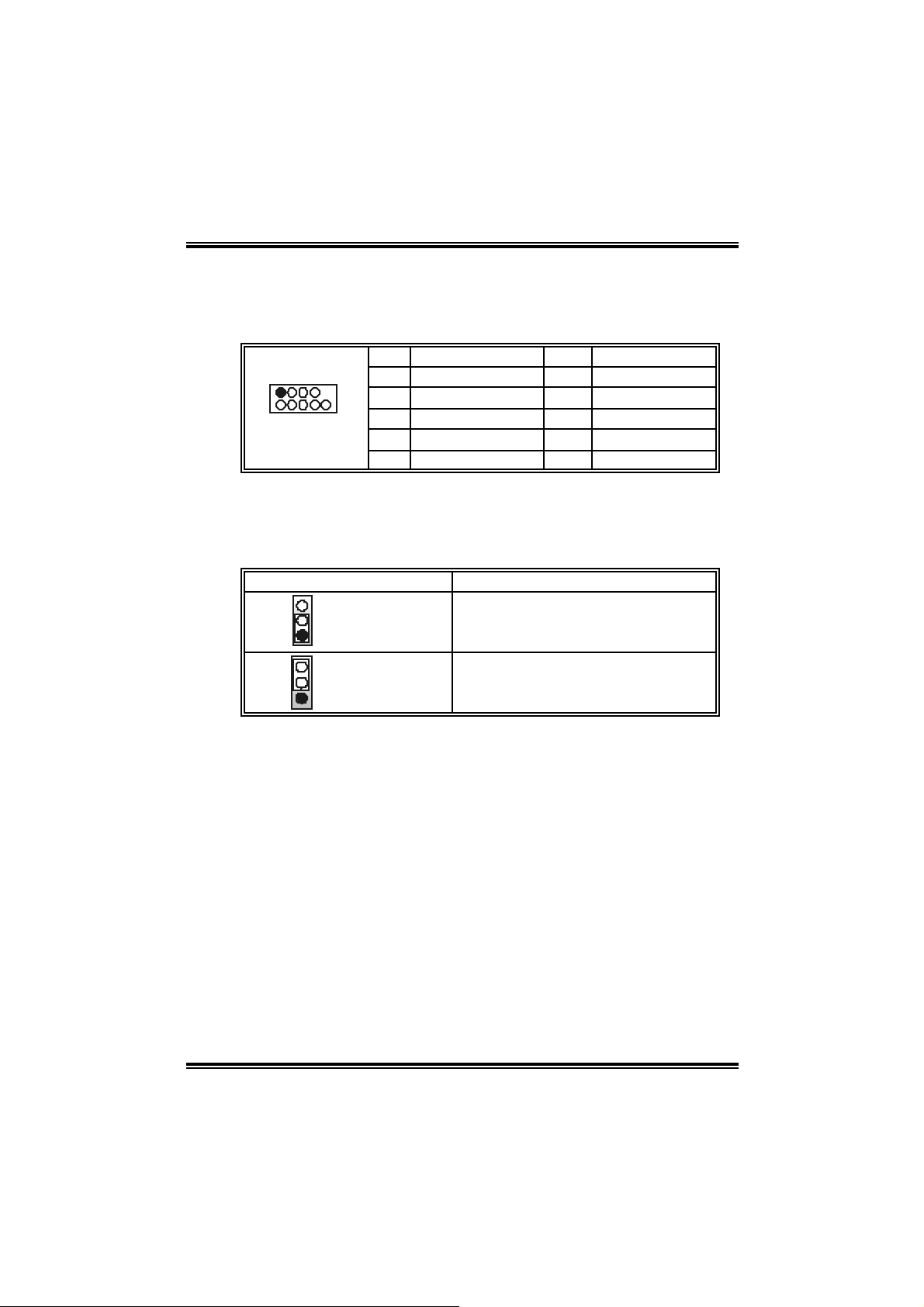
F r ont Pa n el Conn ect or : JPA NEL1
This 24-pin connector includes Power-on, Reset, HDD LED, Power LED,
Sleep button, speaker and IrDA Connection. It allows user to connect
the PC case’s front panel switch functions.
2
1
Pin Assignment Function Pin Assignment Function
1 +5V 2 Sleep control
3 N/A 4 Ground
5 N/A 6 N/A N/A
7 Speaker
9 HDD LED (+) 10 Power LED (+)
11 HDD LED (-)
13 Ground 14 Power button
15 Reset control
17 N/A 18 Key
19 N/A 20 Key
21 +5V 22 Ground
23 IRTX
Speaker
Connector
Hard drive
LED
Reset
button
IrDA
Connector
24
23
JPANEL1
8 Power LED (+)
12 Power LED (-)
16 Ground
24 IRRX
Sleep
button
Power LED
Power-on
button
IrDA
Connector
Case Op en Header: JCI 1
T his connector allows system to mo nitor PC case open statu s. If the
signal has been tri ggered, it will record to the CMOS and show the
message on next boot-up.
Pin Assignment
1
JCI1
1 Cas e open s ignal
2 Ground
16
NF325-A7
Front USB Headers : JUSB1~2
This connector allows user to connect additional USB cables on the PC
front panel . Al so can be connected wi th internal USB devices, like USB
card reader.
Pin Assignment Pin Assignment
1 +5V (fused) 2 +5V (f us ed)
1
2
JUSB1/JUSB2
3 USB- 4 USB-
10
5 USB+ 6 USB+
7 Ground 8 Ground
9 Key 10 NC
Close CMOS He ader : JCMOS 1
By pl aci ng the jumper on pin2-3, i t allows user to restore the BIOS safe
setting and the CMOS data, please careful l y follow the procedures to
avo id da ma ging th e mot her board.
JCMOS1 Assignment
3
1
Pin 1-2 close
3
1
Pin 2-3 close
Norm al Operation (D ef ault).
Clear CMOS data.
※ Clear CMOS Procedures:
1. Remov e AC power line.
2. Set the jumper to “Pin 2-3 cl ose”.
3. Wai t for f i ve seconds.
4. Set the jumper to “Pin 1-2 cl ose”.
5. Power on the AC.
6. Reset your desired password or clear the CMOS data.
17
NF325-A7
CHAPTER 4: USEFUL HELP
4.1 AWAR D BIOS BEEP CODE
Beep Sound Meanin g
One long beep f ollowed by t wo s hort
beeps
High-low siren sound C PU overheated
One Short beep when system boot-up No error found during POST
Long beeps every ot her s econd No DRAM detected or ins t all
4.2 EXTRA INFORMATION
A. BIOS Update
After yo u fail to up d ate BIOS or BIOS is inva ded by virus, the
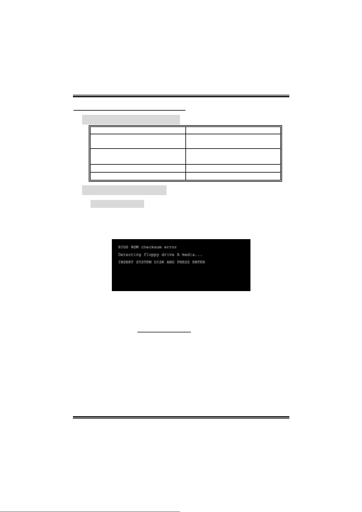
Boot-Block functi on will hel p to restore BIOS. If the following message
is shown after boot-up the system, it m eans the BIOS contents are
corrupted.
Video card not f ound or v ideo card
mem ory bad
Sys t em will s hut down autom at ic ally
In this Case, pl ease follow the procedure below to restore the BIOS:
1. Make a bootable fl op py d is k.
2. Download the Flash Utility “AWDFLASH.exe” from the Bi ostar
websi te: www.biostar.com .tw
3. Confi rm motherboard model and download the respecti vel y BIOS
fr om Bi os t ar websit e.
4. Copy “AWDFLASH.exe” and respectively BIOS into floppy disk.
5. Insert the bootabl e di sk into floppy drive and press Enter.
6. S y stem will boo-up to DOS prompt.
7. Type “Awdflash xxxx.bf/sn/py/r” in DOS prompt.
8. S y stem will update BIOS automa tically and resta rt .
9. The BIOS ha s bee n recovered an d will work pro pe rly.
18
 Loading...