

Page 1
Product Specification
Preliminary Specification
( )
(V ) Final Specification
Module 27” Color TFT-LCD
Model Name M270HTN01.1
AU OPTRONICS CORPORATION
M270HTN01.1
Customer Date
Approved by
Approved by Date
Howard Lee
Prepared by Date
Evelyn Sung
Jul. 03, 2013
Jul. 03, 2013
Note: This Specification is subject to
change without notice.
document version 1.2 1
AU Optronics corporation
Page 2

Product Specification
AU OPTRONICS CORPORATION
M270HTN01.1
Contents
1 Handling Precautions................................................................4
2 General Description ..................................................................5
2.1 Display Characteristics....................................................................................................... 5
2.2 Absolute Maximum Rating of Environment ........................................................................ 6
2.3 Optical Characteristics ....................................................................................................... 7
2.4 Mechanical Characteristics.............................................................................................. 11
3 TFT-LCD Module ......................................................................12
3.1 Block Diagram.................................................................................................................. 12
The following shows the block diagram of the 27 inch Color TFT-LCD Module................ 12
3.2 Interface Connection........................................................................................................ 13
3.2.1 Connector Type............................................................................................................. 13
3.2.2 Connector Pin Assignment............................................................................................ 13
3.3 Electrical Characteristics.................................................................................................. 15
3.3.1 Absolute Maximum Rating ............................................................................................ 15
3.3.2 Recommended Operating Condition............................................................................. 15
3.4 Signal Characteristics ...................................................................................................... 16
3.4.1 LCD Pixel Format.......................................................................................................... 16
3.4.2 LVDS Data Format........................................................................................................ 16
3.4.3 Color versus Input Data ................................................................................................ 17
3.4.4 LVDS Specification........................................................................................................ 18
3.4.5 Input Timing Specification ............................................................................................. 20
3.4.6 Input Timing Diagram.................................................................................................... 21
3.5 Power ON/OFF Sequence ............................................................................................... 22
4 Backlight Unit .........................................................................23
4.1 Block Diagram.................................................................................................................. 23
4.2 Interface Connection........................................................................................................ 24
4.2.1 Connector Type............................................................................................................. 24
Backlight Connector dimension: ............................................................................................ 24
Mating Connector dimension: ................................................................................................ 25
4.2.2 Connector Pin Assignment............................................................................................ 26
4.3 Electrical Characteristics.................................................................................................. 27
4.3.1 Absolute Maximum Rating ............................................................................................ 27
4.3.2 Recommended Operating Condition............................................................................. 27
5 Reliability Test........................................................................29
6 Shipping Label ........................................................................30
7 Mechanical Characteristics .....................................................31
8 Packing Specification..............................................................33
document version 1.2 2
Page 3
Product Specification
cm, package
AU OPTRONICS CORPORATION
M270HTN01.1
Record of Revision
Version
0.1 2013/3/22
1.1 2013/5/24
1.2 2013/6/03
2.2 2013/7/03
Date Page Old description New Description Remark
All First version release -
3.4.5 Input Timing Specification
3.2.1 Connector Type
Power Consumption
25.84 (Typ.) LCD module : PDD
(Typ.)=5.5 @ Black
pattern,Fv=75Hz
3.2.2 Connector Pin Assignment
20
13
5
3.4.5 Input Timing Specification
3.2.1 Connector Type
Power Consumption
25.67 (Typ.) LCD module : PDD
(Typ.)=5.33 @ Black
pattern,Fv=75Hz
3.2.2 Connector Pin Assignment
13
15
27
27
3.3.2 Recommended Operating
Condition
4.3.1 Absolute Maximum Rating
LED String Current Max.300 mA
4.3.2 Recommended Operating
Condition
LED Light Bar Power
Consumption Max. 24.7 Watt
3.3.2 Recommended Operating
Condition
4.3.1 Absolute Maximum Rating
LED String Current Max.210 mA
4.3.2 Recommended Operating
Condition
LED Light Bar Power
Consumption Max. 22.5 Watt
28
2.3 2013/7/26
document version 1.2 3
29
Drop Test Height: 60
test
Add Note 4-5 & Note 4-6
Drop Test Height: 45.7 cm,
package test
Page 4

Product Specification
AU OPTRONICS CORPORATION
M270HTN01.1
1 Handling Precautions
1) Since front polarizer is easily damaged, pay attention not to scratch it.
2) Be sure to turn off power supply when inserting or disconnecting from input connector.
3) Wipe off water drop immediately. Long contact with water may cause discoloration or spots.
4) When the panel surface is soiled, wipe it with absorbent cotton or other soft cloth.
5) Since the panel is made of glass, it may break or crack if dropped or bumped on hard
surface.
6) Since CMOS LSI is used in this module, take care of static electricity and insure human earth
when handling.
7) Do not open or modify the Module Assembly.
8) Do not press the reflector sheet at the back of the module to any directions.
9) In case a TFT-LCD Module has to be put back into the packing container slot after once it
was taken out from the container, do not press the center of the LED lightbar edge. Otherwise
the TFT-LCD Module may be damaged.
10) Insert or pull out the interface connector, be sure not to rotate nor tilt it of the TFT-LCD
Module.
11) Do not twist nor bend the TFT -LCD Module even momentary. It should be taken into
consideration that no bending/twisting forces are applied to the TFT-LCD Module from
outside. Otherwise the TFT-LCD Module may be damaged.
12) Please avoid touching COF position while you are doing mechanical design.
13) When storing modules as spares for a long time, the following precaution is necessary:
Store them in a dark place. Do not expose the module to sunlight or fluorescent light. Keep
the temperature between 5℃ and 35℃ at normal humidity.
document version 1.2 4
Page 5
Product Specification
AU OPTRONICS CORPORATION
M270HTN01.1
2 General Description
This specification applies to the 27 inch wide Color a-Si TFT-LCD Module M270HTN01.1. The
display supports the Full HD - 1920(H) x 1080(V) screen format and 16.7M colors (RGB 6-bits +
Hi-FRC data). The input interface is tow channel LVDS and this module doesn’t contain an driver
board for backlight.
2.1 Display Characteristics
The following items are characteristics summary on the table under 25℃ condition:
ITEMS Unit SPECIFICATIONS
Screen Diagonal [mm] 685.65(27”)
Active Area [mm] 597.6 (H) x 336.15 (V)
Pixels H x V - 1920(x3) x 1080
Pixel Pitch [um] 311.25 (per one triad) ×311.25
Pixel Arrangement - R.G.B. Vertical Stripe
Display Mode - TN Mode, Normally White
White Luminance ( Center ) [cd/m2] 300 (Typ.)
Contrast Ratio - 1000:1 (Typ.)
Response Time [msec] 5ms (Typ., on/off)
Power Consumption
(LCD Module + Backligh unit)
Weight [Grams] 2860
Outline Dimension [mm] 630 (W) × 368.2 (H) × 14.1(D)
Electrical Interface - Two channel LVDS
Support Color - 16.7M colors (RGB 6-bit + Hi_FRC )
Surface Treatment - Anti-Glare, 3H
Temperature Range
Operating
Storage (Shipping)
RoHS Compliance - RoHS Compliance
TCO Compliance - TCO 6.0 Compliance
[Watt] 25.84 (Typ.)
LCD module : PDD (Typ.)=5.5 @ Black pattern,Fv=75Hz
Backlight unit : P
[oC]
[oC]
0 to +50
-20 to +60
(Typ.) =20.34 @Is=120mA
BLU
document version 1.2 5
Page 6

Product Specification
AU OPTRONICS CORPORATION
M270HTN01.1
2.2 Absolute Maximum Rating of Environment
Permanent damage may occur if exceeding the following maximum rating.
Symbol Description Min. Max. Unit Remark
TOP Operating Temperature 0 +50 [℃] Note 2-1
TGS
Glass surface temperature
(operation)
0 +65 [℃]
Function judged only
HOP Operation Humidity 5 90 [%RH]
TST Storage Temperature -20 +60 [℃]
HST Storage Humidity
5 90
[%RH]
Note 2-1: Temperature and relative humidity range are shown as the below figure.
1. 90% RH Max ( Ta ≦39 ℃)
2. Max wet-bulb temperature at 39 ℃ or less. ( Ta ≦39 ℃)
3. No condensation
Note 2-1
Note 2-1
Operating Range Storage Range
document version 1.2 6
Page 7
Product Specification
AU OPTRONICS CORPORATION
2.3 Optical Characteristics
The optical characteristics are measured on the following test condition.
Test Condition:
1. Equipment setup: Please refer to Note 2-2.
2. Panel Lighting time: 30 minutes
3. VDD=5.0V, Fv=75Hz,Is=120mA,Ta=25 ℃
M270HTN01.1
Symbol
Lw
L
uni
CR
θR
θL
ΦH
ΦL
θR
θL
ΦH
ΦL
TR
TF
-
Rx
Ry
Gx
Gy
Bx
By
Wx
Wy
CT
FdB
Description Min. Typ. Max. Unit Remark
White Luminance (Center of screen)
Luminance Uniformity (9 points)
Contrast Ratio (Center of screen) 600 1000
Horizontal Viewing Angle
(CR=10)
Vertical Viewing Angle
(CR=10)
Horizontal Viewing Angle
(CR=5)
Vertical Viewing Angle
(CR=5)
Response Time
Color Coordinates
(CIE 1931)
Crosstalk - -
Flicker (Center of screen) - -
Right 75 85 -
Left 75 85 -
Up
Down 70 80 -
Right 75 88 -
Left 75 88 -
Up
Down 70 85 -
Rising Time - 3.8
Falling Time -
Rising + Falling -
Red x 0.617
Red y
Green x
Green y
Blue x
Blue y
White x
White y
240 300
75 80
70 80 -
70 85 -
0.312 0.342 0.372
0.288 0.318 0.348
0.601 0.631 0.661
0.120 0.150 0.180
0.020 0.050 0.080
0.283 0.313 0.343
0.299 0.329 0.359
-
-
- -
5.5
1.2 2.5
5 8
0.647 0.677
1.5
-20
2
[
cd/m
[%]
[degree]
[msec]
-
[%]
[dB]
Note 2-2
]
By SR-3
Note 2-3
By SR-3
Note 2-4
By SR-3
Note 2-5
By SR-3
Note 2-6
By TRD-100
By SR-3
Note 2-7
By SR-3
Note 2-8
By SR-3
document version 1.2 7
Page 8
Note 2-2: Equipment setup :
Product Specification
AU OPTRONICS CORPORATION
Photo detector (SR-3, TRD-100)
Measured distance (50cm)
M270HTN01.1
Center of the screen
Note 2-3: Luminance Uniformity Measurement
Definition:
y UniformitLuminance =
a.Test pattern: White Pattern
P9)~(P1 Points 9 of Luminance Minimum
P9)~(P1 Points 9 of Luminance Maximum
document version 1.2 8
Page 9
Product Specification
100
90
W hite
100
White
Black
Black
1 Frame
1 Frame
AU OPTRONICS CORPORATION
M270HTN01.1
Note 2-4: Contrast Ratio Measurement
Definition:
RatioContrast =
a. Measured position: Center of screen (P5) & perpendicular to the screen (θ=Φ=0°)
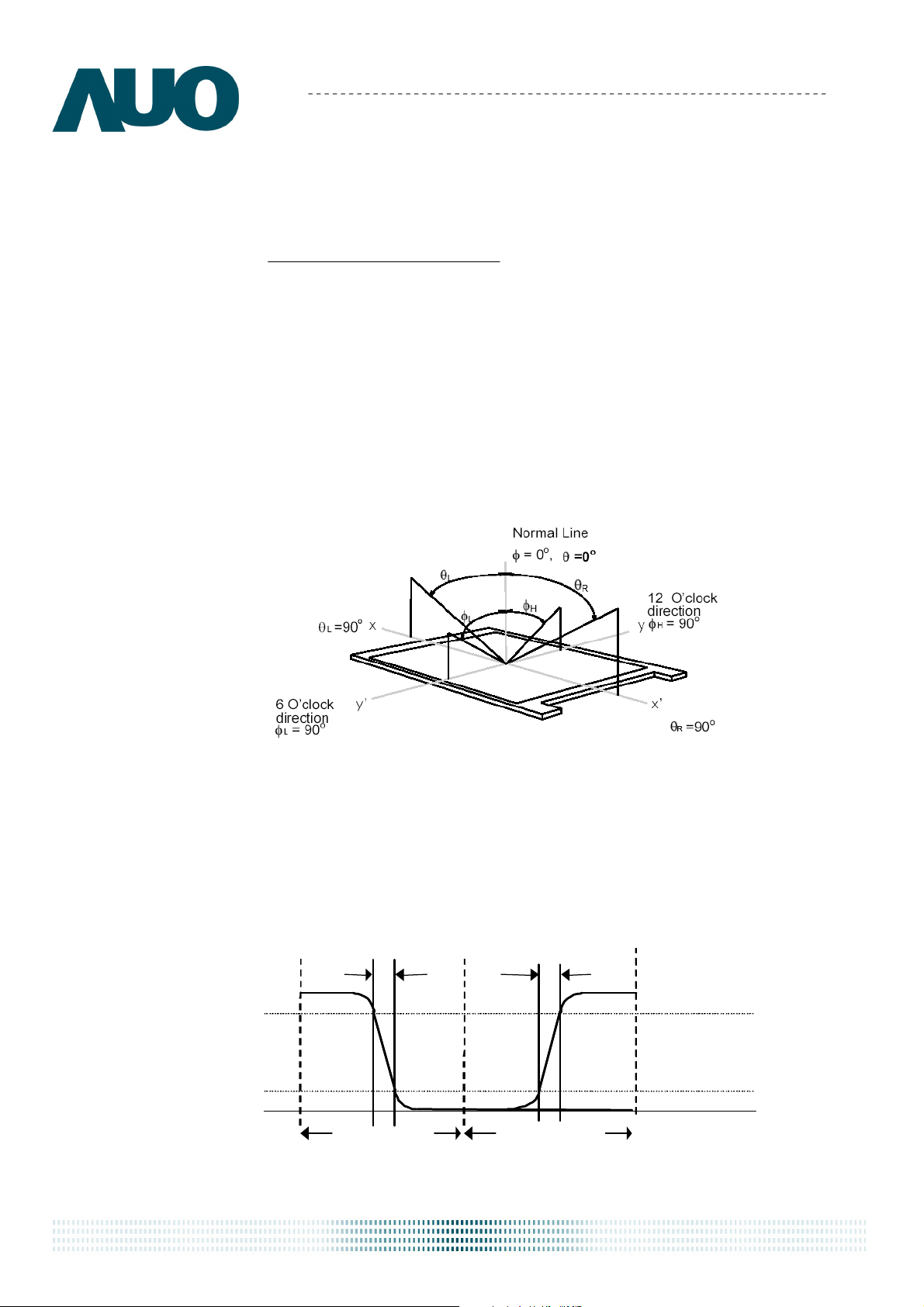
Note 2-5: Viewing angle measurement
Definition: The angle at which the contrast ratio is greater than 10 & 5 .
a. Horizontal view angle: Divide to left & right (θL & θR)
Vertical view angle: Divide to up & down (ΦH &ΦL)
pattern Whiteof Luminance
pattern Black of Luminance
Note 2-6: Response time measurement
The output signals of photo detector are measured when the input signals are changed
from “Black” to “White” (rising time, TR), and from “White” to “Black” (falling time, TF),
respectively. The response time is interval between the 10% and 90% of optical
response. (Black & White color definition: Please refer section 3.4.3)
%
%
Optical
Optical
respon se
respon se
10
10
0
0
document version 1.2 9
T
F
T
R
Page 10
Product Specification
AU OPTRONICS CORPORATION
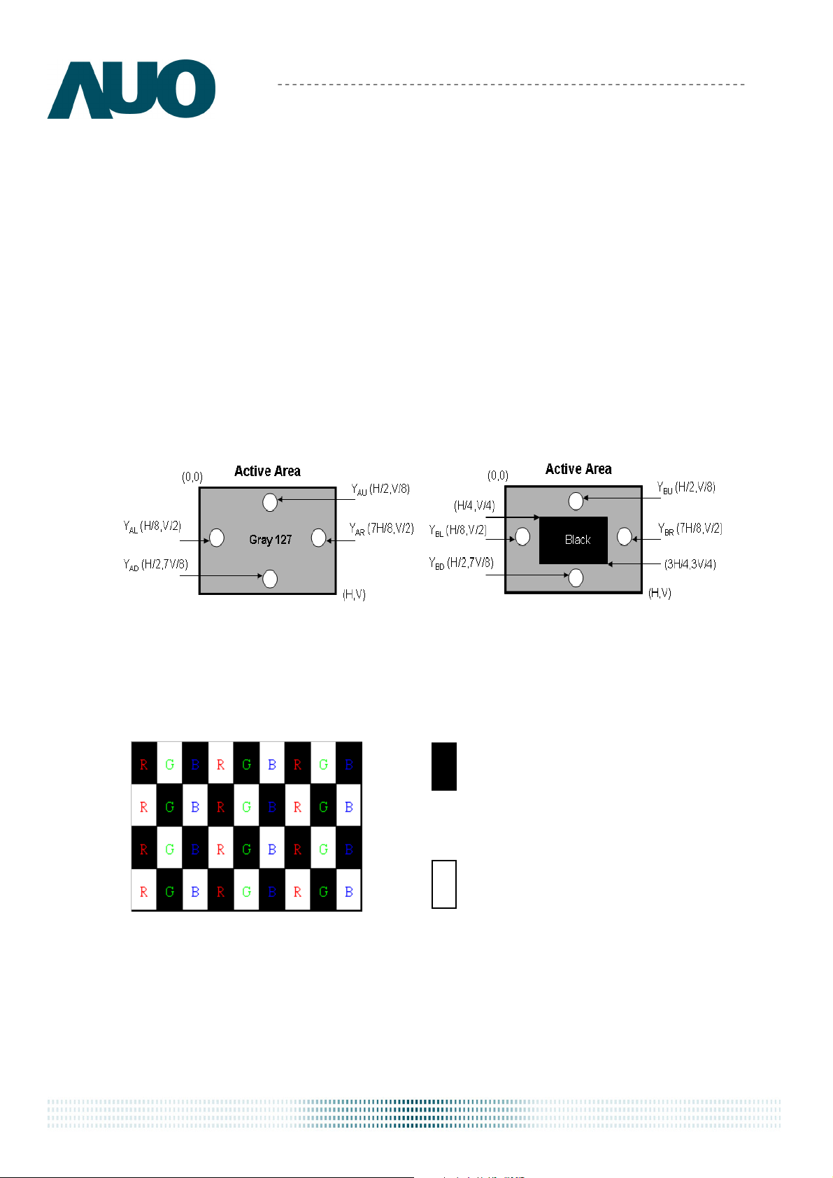
Note 2-7: Crosstalk measurement
Definition:
CT = Max. (CTH,CTV);
Where
a.Maximum Horizontal Crosstalk :
CTH = Max. (| YBL – YAL | / YAL × 100 %, | YBR – YAR | / YAR × 100 %);
Maximum Vertical Crosstalk:
CTV = Max. (| YBU – YAU | / YAU × 100 %, | YBD – YAD | / YAD × 100 %);
b. YAU, YAD, YAL, YAR = Luminance of measured location without Black pattern
YBU, YBD, YBL, YBR = Luminance of measured location with Black pattern
M270HTN01.1
Note 2-8: Flicker measurement
a. Test pattern: It is listed as following.
Gray level = L0
Gray level = L127
R: Red, G: Green, B:Blue
b. Measured position: Center of screen (P5) & perpendicular to the screen (θ=Φ=0°)
document version 1.2 10
Page 11
Product Specification
AU OPTRONICS CORPORATION
M270HTN01.1
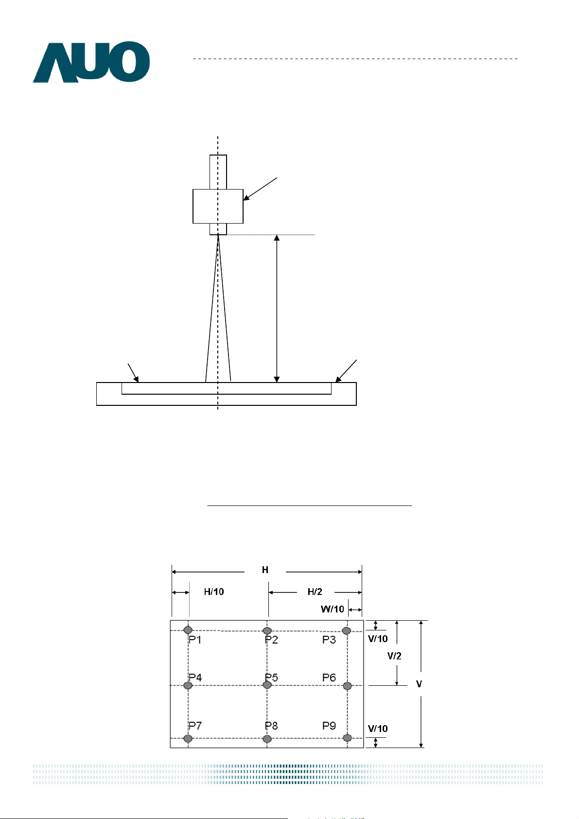
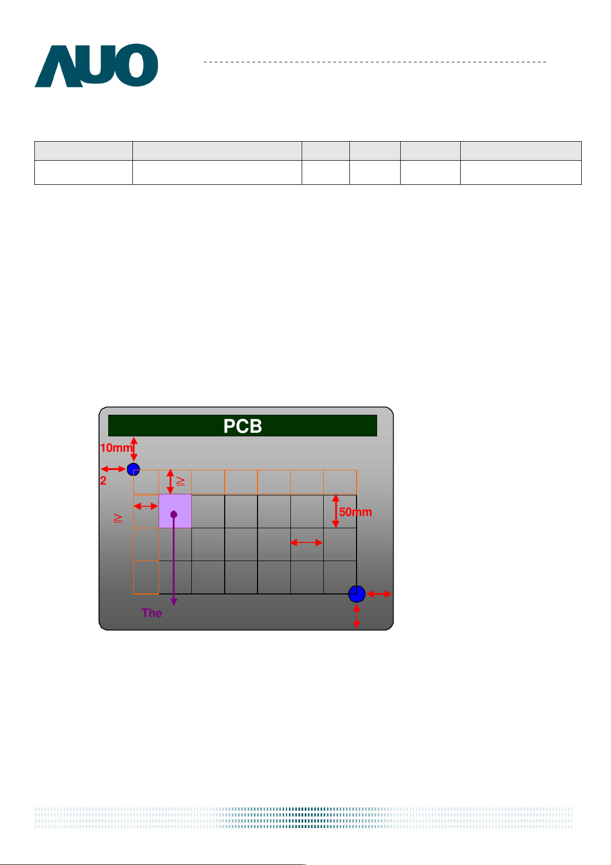
2.4 Mechanical Characteristics
Symbol Description Min. Max. Unit Remark
Pbc Backside Compression
2.5 - [Kgf] Note 2-9
Note 2-9: Test Method:
The point is at a distance from right-downside 25mm x 25mm defined as the Start Point
of Measure Points, and the point is at a distance 25mm from left-side & around 10mm
from PCB defined as the End Point.
Align 50mm x 50mm block from Start Point on the Bezel Back, and the corners of each
block are Measure Points.
If the distance from the last block to each side of the End Point ≧ 25mm, add other
blocks to make sure that most area of Bezel Back can be measured.
10mm
10mm
25mm
25mm
≧≧≧≧
25mm
≧≧≧≧
25mm
End Point
End Point
≧≧≧≧
25mm
≧≧≧≧
25mm
The last block
The last block
PCB
PCB
50mm
50mm
50mm
50mm
Start Point
Start Point
25mm
25mm
25mm
25mm
document version 1.2 11
Page 12

Product Specification
VDD
AUO ASIC
Connector
G
108
0
D
576
0
AU OPTRONICS CORPORATION
M270HTN01.1
3 TFT-LCD Module
3.1 Block Diagram
The following shows the block diagram of the 27 inch Color TFT-LCD Module.
LVDS
Signal
DC/DC
Converter
Receiver
LVDS
Control Board
Correction
ASIC
Gamma
Timing
Controller
Mini LVDS
Transmitter
D1
G1
TFT-LCD
1920(x3) x 1080
Pixels
document version 1.2 12
Page 13

Product Specification
AU OPTRONICS CORPORATION
3.2 Interface Connection
3.2.1 Connector Type
TFT-LCD Connector
Mating Connector
3.2.2 Connector Pin Assignment
PIN # Symbol Description
1 RxO0- Negative LVDS differential data input (Odd data)
Manufacturer P-Two STM
Part Number
Manufacturer JAE
Part Number FI-X30HL (Locked Type)
AL230F-A0G1D-P
M270HTN01.1
MSCKT2407P30HB
2 RxO0+ Positive LVDS differential data input (Odd data)
3 RxO1- Negative LVDS differential data input (Odd data)
4 RxO1+ Positive LVDS differential data input (Odd data)
5 RxO2- Negative LVDS differential data input (Odd data)
6 RxO2+ Positive LVDS differential data input (Odd data)
7 GND Ground
8 RxOCLK- Negative LVDS differential clock input (Odd clock)
9 RxOCLK+ Positive LVDS differential clock input (Odd clock)
10 RxO3- Negative LVDS differential data input (Odd data)
11 RxO3+ Positive LVDS differential data input (Odd data)
12 RxE0- Negative LVDS differential data input (Even data)
13 RxE0+ Positive LVDS differential data input (Even data)
14 GND Ground
15 RxE1- Negative LVDS differential data input (Even data)
16 RxE1+ Positive LVDS differential data input (Even data)
17 GND Ground
18 RxE2- Negative LVDS differential data input (Even data)
19 RxE2+ Positive LVDS differential data input (Even data)
20 RxECLK- Negative LVDS differential clock input (Even clock)
21 RxECLK+ Positive LVDS differential clock input (Even clock)
22 RxE3- Negative LVDS differential data input (Even data)
23 RxE3+ Positive LVDS differential data input (Even data)
24 GND Ground
25 NC No connection (for AUO test only. Do not connect)
document version 1.2 13
Page 14

Product Specification
AU OPTRONICS CORPORATION
M270HTN01.1
26 NC No connection (for AUO test only. Do not connect)
27 NC No connection (for AUO test only. Do not connect)
28 VDD Power Supply Input Voltage
29 VDD Power Supply Input Voltage
30 VDD Power Supply Input Voltage
document version 1.2 14
Page 15

Product Specification
AU OPTRONICS CORPORATION
3.3 Electrical Characteristics
3.3.1 Absolute Maximum Rating
Permanent damage may occur if exceeding the following maximum rating.
M270HTN01.1
Symbol
VDD
Description Min Max Unit
Power Supply
Input Voltage
GND-0.3 6.0 [Volt]
3.3.2 Recommended Operating Condition
Symbol
VDD
IDD
PDD
IRush Inrush Current
VDDrp
Description Min Typ Max Unit
Power supply
Input voltage
Power supply
Input Current
(RMS)
VDD Power
Consumption
Allowable VDD
Ripple Voltage
4.5 5.0 5.5 [Volt]
- 0.9 1.1
1.1 1.3
- 4.5 5.5
5.5 6.5
-
-
- 3.0 [A]
- 500 [mV]
[A]
[A]
[Watt]
[Watt]
Remark
Ta=25 ℃
Remark
VDD= 5.0V, Black Pattern, Fv=60Hz
VDD= 5.0V, Black Pattern, Fv=75Hz
VDD= 5.0V, Black Pattern, Fv=60Hz
VDD= 5.0V, Black Pattern, Fv=75Hz
Note 3-1
VDD= 5.0V, Black Pattern, Fv=75Hz
Note 3-1: Inrush Current measurement:
Test circuit:
The duration of VDD rising time: 470us.
document version 1.2 15
Page 16

R G B R G B
R G B R G B
R G B R G B
R G B R G B
1 2 1
919 1
920
1st Line
1080
Line
3.4 Signal Characteristics
3.4.1 LCD Pixel Format
Product Specification
AU OPTRONICS CORPORATION
M270HTN01.1
3.4.2 LVDS Data Format
Note 3-2:
a. O = “Odd Pixel Data” E = “Even Pixel Data”
b. Refer to 3.4.1 LCD pixel format, the 1st data is 1 (Odd Pixel Data), the 2nd data is 2 (Even Pixel Data) and
the last data is 1920 (Even Pixel Data).
document version 1.2 16
Page 17

Product Specification
M270HTN01.1
AU OPTRONICS CORPORATION
3.4.3 Color versus Input Data
The following table is for color versus input data (8bit). The higher the gray level, the brighter
the color.
document version 1.2 17
Page 18

3.4.4 LVDS Specification
Product Specification
AU OPTRONICS CORPORATION
M270HTN01.1
a. DC Characteristics:
Symbol
VTH
VTL
│VID│
VCM
Description Min Typ Max Units
LVDS Differential
Input High Threshold
LVDS Differential
Input Low Threshold
LVDS Differential
Input Voltage
LVDS Common Mode
Voltage
-100
100 - 600 [mV]
+1.0 +1.2 +1.5 [V] VTH-VTL = 200mV
LVDS Signal Waveform:
Use RxOCLK- & RxOCLK+ as example.
RxOCLK-
Condition
- - +100 [mV] VCM = 1.2V
- - [mV] VCM = 1.2V
RxOCLK+
document version 1.2 18
Page 19

Product Specification
Freq
F
max
F
clk
F
min
F
clk
* F
DEV
< Spread Spectrum>
T
ime
AU OPTRONICS CORPORATION
b. AC Characteristics:
Symbol Description Min Max Unit Remark
Maximum deviation of
F
DEV
input clock frequency
during Spread Spectrum
Maximum modulation
F
MOD
frequency of input clock
during Spread Spectrum
- ± 3 %
- 200 KHz
M270HTN01.1
Fclk: LVDS Clock Frequency
F
1
MOD
document version 1.2 19
Page 20

Product Specification
AU OPTRONICS CORPORATION
3.4.5 Input Timing Specification
It only support DE mode, and the input timing are shown as the following table.
Symbol Description Min. Typ. Max. Unit
M270HTN01.1
Remark
Tv Period
Tdisp (v) Active
Vertical Section
Tblk (v) Blanking
Fv
Frequency
Th Period
Tdisp (h) Active
Horizontal Section
Tblk (h) Blanking
Fh
Frequency 55 68 91 KHz
Tclk Period
LVDS Clock
Fclk
Frequency
1092 1130 1818
1080 1080 1080
12 50 738
50 60 76
1034 1050 1100
960 960 960
74 90 140
10.6 14.0 17.7
56.5 71.2 94.0
Th
Th
Th
Hz
Tclk
Tclk
Tclk
Note 3-3
ns 1/Fclk
MHz
Note 3-4
Note 3-3: The equation is listed as following. Please don’t exceed the above recommended value.
Fh (Min.) = Fclk (Min.) / Th (Min.);
Fh (Typ.) = Fclk (Typ.) / Th (Typ.);
Fh (Max.)= Fclk (Max.) / Th (Min.);
Note 3-4: The equation is listed as following. Please don’t exceed the above recommended value.
Fclk (Min.) = Fv (Min.) x Th (Min.) x Tv (Min.);
Fclk (Typ.) = Fv (Typ.) x Th (Typ.) x Tv (Typ.);
Fclk (Max.) = Fv (Max.) x Th (Typ.) x Tv (Typ.);
document version 1.2 20
Page 21

3.4.6 Input Timing Diagram
DE
RGB Data
CLK
DE
RGB Data
(Odd)
RGB Data
(Even)
N
Line
Pixel
M-7
Pixel
M-6
Pixel
M-5
Pixel
Pixel
M-3
Pixel
M-2
Tblk(v)
Invalid Data
Tclk
Pixel
M-1
Pixel
M
Invalid Data
Invalid Data
Product Specification
AU OPTRONICS CORPORATION
Tv
Tdisp(v)
Th
32
LineLine
Th
Tdisp(h)
Pixel
Pixel
10
4
LineLine
Pixel
Pixel
119
Pixel
12
1
Pixel
1
Pixel Pixel
2
Pixel
Pixel
3
4
Pixel
7
5
Pixel
Pixel
6 M-2
8 M
N
Line
M-5
M-4
Pixel
M-3
Pixel
Pixel
M-1
PixelPixel
M270HTN01.1
M pixel
Y
N Line
Invalid Data
Tblk(h)
Invalid Data
Invalid Data
X
Pixel
1
Pixel
2M-4
Pixel
3
Pixel
4
document version 1.2 21
Page 22

Product Specification
10%
90%
10%
90%
AU OPTRONICS CORPORATION
M270HTN01.1
3.5 Power ON/OFF Sequence
VDD power,LVDS signal and backlight on/off sequence are as following. LVDS signals
from any system shall be Hi-Z state when VDD is off.
Backlight Off
T1
LVDS Signal
Symbol
VDD
V
SLED
Backlight Off
T2
VALID
T3
Backlight On
Power Sequence Timing
T5
T4
Backlight Off
T6
T7
Value Remark
Unit
Min. Typ. Max.
T1 0.5 - 10 [ms]
T2 0 - 50 [ms]
T3 500 - - [ms]
T4 100 - - [ms]
T5 0 50 [ms]
T6 0 - 100 [ms]
T7 1000 - - [ms]
Note 3-5
Note 3-6
Note 3-6
Note 3-5 : Recommend setting T5 = 0ms to avoid electronic noise when VDD is off.
Note 3-6 : During T5 and T6 period , please keep the level of input LVDS signals with Hi-Z state.
document version 1.2 22
Page 23

Product Specification
V
SLED
S
Ch1
Ch2
Ch3
Ch4
AU OPTRONICS CORPORATION
4 Backlight Unit
4.1 Block Diagram
The following shows the block diagram of the 27 inch Backlight Unit. And it includes 52 pcs LED in
the LED light bar. (4 strings and 13 pcs LED of one string).
M270HTN01.1
+
V
-
I
S
I
S
I
S
Connector
I
S
document version 1.2 23
Page 24

Product Specification
==××=××
AU OPTRONICS CORPORATION
4.2 Interface Connection
4.2.1 Connector Type
Backlight Connector
Mating Connector
Backlight Connector dimension:
Manufacturer ENTERY
Part Number 3707K-S06N-21R
Manufacturer ENTERY
Part Number
M270HTN01.1
H112K-P06N-00B (Non-Locking type)
H112K-P06N-03B (Locking type)
)(0.1,25.400.39.13 mmunitPitchDVH
document version 1.2 24
Page 25

Mating Connector dimension:
Product Specification
M270HTN01.1
AU OPTRONICS CORPORATION
document version 1.2 25
Page 26

Product Specification
AU OPTRONICS CORPORATION
M270HTN01.1
4.2.2 Connector Pin Assignment
Pin# Symbol Description Remark
1 Ch1 LED Current Feedback Terminal (Channel 1)
2 Ch2 LED Current Feedback Terminal (Channel 2)
3 V
4 V
LED Power Supply Voltage Input Terminal
SLED
LED Power Supply Voltage Input Terminal
SLED
5 Ch3 LED Current Feedback Terminal (Channel 3)
6 Ch4 LED Current Feedback Terminal (Channel 4)
document version 1.2 26
Page 27

Product Specification
AU OPTRONICS CORPORATION
M270HTN01.1
4.3 Electrical Characteristics
4.3.1 Absolute Maximum Rating
Permanent damage may occur if exceeding the following maximum rating.
Symbol Description Min Max Unit Remark
(Ta=25℃)
Is
LED String Current 0
Duty ratio= (A / B) X 100% ; (A: Pulse time, B: Period)
4.3.2 Recommended Operating Condition
Symbol
Description
Is LED String Current -
Min.
Typ. Max. Unit Remark
120 132
150
210
[mA]
[mA]
[mA]
100% duty ratio
Duty ratio≦ 10%
Pulse time=10 ms
(Ta=25℃)
100% duty ratio of LED
chip
Vs LED String Voltage
∆Vs
Maximum Vs Voltage
Deviation of light bar
LED Light Bar Power
P
BLU
LT
LED
document version 1.2 27
Consumption
LED Life Time 30,000
39 42.9 46.8
-
-
- 2.6
20.6 22.5
- - [Hour]
[Volt]
[Volt]
[Watt]
Is=120mA @ 100% duty
ratio; Note 4-1, Note 4-5
Is=120mA @ 100% duty
ratio; Note 4-2
Note 4-3
Note 4-4
Page 28

Product Specification
AU OPTRONICS CORPORATION
Note 4-1: Vs (Typ.) = VF (Typ.) X LED No. (one string);
a. VF: LED chip forward voltage, VF (Min.)=3.0V, VF(Typ.)=3.3V, VF(Max.)=3.6V
b. The same euqation to calculate Vs(Min.) & Vs (Max.) for respective VF (Min.) &
VF(Max.);
M270HTN01.1
Note 4-2: ∆Vs (Max.) = ∆VF X LED No. (one string);
a. ∆V
Note 4-3: P
P
BLU
BLU
LED chip forward voltage deviation; (0.2 V , each Bin of LED VF)
F:
(Typ.) = Vs (Typ.) X Is (Typ.) X 4 ; ( 4 is total String No. of LED Light bar)
(Max.) = Vs (Max.) X Is (Typ.) X 4 ;
Note 4-4: Definition of life time:
a. Brightness of LED becomes to 50% of its original value
b. Test condition: Is = 120mA and 25 ℃ (Room Temperature)
Note 4-5: Recommendation for LED driver power design:
Due to there are electrical property deviation in LED & monitor set system component
after long time operation. AUO strongly recommend the design value of LED driver
board OVP (over voltageprotection) should be 10% higher than max. value of LED
string voltage (Vs) at least.
Note 4-6: AUO strongly recommend “Analog Dimming” method for backlight brightness control
for Wavy Noise Free. Otherwise, recommend that Dimming Control Signal (PWM
Signal) should be synchronized with Frame Frequency.
document version 1.2 28
Page 29

KV, 150pF(330Ω ) 1sec,
Air Discharge: ± 15KV, 150pF(330Ω ) 1sec
5 Reliability Test
Product Specification
AU OPTRONICS CORPORATION
M270HTN01.1
AUO reliability test items are listed as following table. (Bare Panel only)
Items Condition
Temperature Humidity Bias (THB)
High Temperature Operation (HTO)
Low Temperature Operation (LTO)
High Temperature Storage (HTS)
Low Temperature Storage (LTS)
Vibration Test
(Non-operation)
Shock Test
(Non-operation)
Drop Test Height: 45.7 cm, package test
Ta= 50
Ta= 50
Ta= 0
Ta= 60
Ta= -20
Acceleration: 1.5 Grms
Wave: Random
Frequency: 10 - 200 Hz
Sweep: 30 Minutes each Axis (X, Y, Z)
Acceleration: 50 G
Wave: Half-sine
Active Time: 20 ms
Direction: ±X, ±Y, ±Z (one time for each Axis)
℃
, 80%RH, 300hours
℃
, 50%RH, 300hours
℃
, 300hours
℃
, 300hours
℃
, 300hours
Remark
Thermal Shock Test (TST)
On/Off Test On/10sec, Off/10sec, 30,000 cycles
ESD (Electro Static Discharge)
Altitude Test
-20 °C /30min, 60
Contact Discharge: ± 15
8 points, 25 times/ point.
8 points, 25 times/ point.
Operation:18,000 ft
Non-Operation:40,000 ft
℃
/30min, 100 cycles
Note 5-1
Note 5-2
Note 5-1: a. A cycle of rapid temperature change consists of varying the temperature from -20 ℃
to 60 °C, and back again. Power is not applied during the test.
b. After finish temperature cycling, the unit is placed in normal room ambient for at least
4 hours before power on.
Note 5-2: EN61000-4-2, ESD class B: Certain performance degradation allowed
No data lost
Self-recoverable
No hardware failures.
document version 1.2 29
Page 30

Product Specification
AU OPTRONICS CORPORATION
6 Shipping Label
The label is on the panel as shown below:
Note 6-1: For Pb Free products, AUO will add for identification.
M270HTN01.1
M270HTN01.1
Note 6-2: For RoHS compatible products, AUO will add for identification.
Note 6-3: For China RoHS compatible products, AUO will add for identification.
Note 6-4: The Green Mark will be presented only when the green documents have been ready by
AUO Internal Green Team.
document version 1.2 30
Page 31

7 Mechanical Characteristics
Avoid touching COF position when doing mechanical design
31
Page 32

32
Page 33

8 Packing Specification
33
Page 34

Pallet and shipment information
Item
Remark
Q'ty Dimension Weight(kg)
630(H)mm x 368.2(V)mm x
Specification
1 Panel 1
2.86
14.1(D)mm
2 Cushion 1 - 2.97
3 Box 1
4 Packing Box 7 pcs/Box
720(L)mm x 264(W)mm x
1.43
455(H)mm
720(L)mm x 264(W)mm x
26.80
455(H)mm
without Panel &
cushion
with panel &
cushion
1070(L)mm x 740(W)mm x
5 Pallet 1
12
140(H)mm
Pallet after
6
Packing
8 boxes/pallet
1070(L)mm x 740(W)mm x
262.48
140(H)mm
34
 Loading...