

查询TDA1083供应商
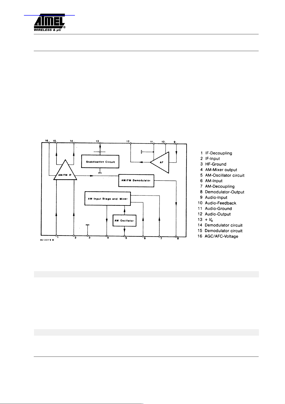
One Chip AM/FM Radio with Audio Power Amplifier
Description
The integrated circuit TDA1083 includes, with exception
of the FM front end, a complete AM-/FM-radio-circuit
with audio power amplifier. An internal Z-diode
Features
Large supply voltage range V
High AM-Sensitivity
= 3 to 12 V
S
stabilizes the supply voltage at VS 13 V, which allows
with the aid of a resistor and a rectifier, the circuit to be
driven by a higher external supply voltage.
AFC-connection for VHF-tuner
AM-FM switching without high frequency voltages
TDA1083
Limiting threshold voltage V
Audio output power P0 = 0.7 W
i
= 50 V
Figure 1. Block diagram and pin connections
Applications
AM-/FM- and audio-amplifier
Absolute Maximum Ratings
Reference points Pin 3 and 11, unless otherwise specified
Parameters Symbol Value Unit
Supply voltage range Pin 13 V
Supply current when using the integrated stabilization
circuit, V
Power dissipation T
Junction temperature T
Storage temperature range T
= 12.5 to 14.3 V Pin 13 I
S
= 65°C P
amb
s
S
tot
j
stg
3 to 12 V
50 mA
600 mW
125 °C
–25 to +125 °C
Thermal Resistance
Parameters Symbol Maximum Unit
Junction ambient R
Rev. A2, 23–Feb–01 1 (8)
thJA
100 K/W

TDA1083
Electrical Characteristics
V
= 9 V, reference points Pin 3 and 11, T
s
Parameters Test Conditions / Pin Symbol Min Typ Max Unit
AF amplifier
AF voltage amplification f = 1 kHz G
Input impedance R
Output power Figures 4 and 5
V
= 5.5 V,
S
R
= 8 , k = 10%
L
AM-IF amplifier, f
DC voltages at AM mode
= 1 MHz, fIF = 455 kHz, f
i
V
= 3 V Pin 10
S
without signal
I
= 42 mA Pin 10
S
(V
= 12.5 to14.3 V)
S
Regulation range V
oAF/VoAF
AF voltage at demodulator
output
FM-IF amplifier, f
DC voltages at FM mode
= 10.7 MHz, f = 22.5 kHz, f
IF
V
= 3 V Pin 10
S
without signal
= 25°C, unless otherwise specified
amb
= 1 kHz, m = 0.3
mod
Pin 12
Pin 13
Pin 16
Pin 12
Pin 13
Pin 16
= –10 dB
Pin 6 V
Pin 8 V
= 1 kHz
mod
Pin 12
Pin 13
Pin 16
V
V
V
V
V
V
V
V
V
V
V
V
P
10
12
13
16
10
12
13
16
oAF
10
12
13
16
v
i
o
300 mW
1.0
3.0
1.25
40 dB
150 k
1.2
3.0
1.2
1.4
3.0
2.0
7.2
V
V
V
V
V
V
5.9
12.5
1.5
i
13.3
14.3
2.0
70 dB
V
V
100 mV
1.0
3.0
1.8
1.2
3.0
1.4
3.0
2.8
V
V
V
V
I
= 42 mA Pin 10
S
(V
= 12.5 to 14.3 V)
S
Pin 12
Pin 13
Pin 16
Limiting threshold (–3 dB) Pin 2 V
AF voltage at demodulator
Pin 8 V
output
Different dc voltages are developed at Pin 16 due to gain
Table 1. Available in following voltage groups:
spread of AM-IF-amplifier. To determine the value of
parallel resistance R8, at the output of the demodulator
Pin 8 for VS = 9 V, AM mode without signal, dc voltage
should be selected at Pin 16.
V
10
1.2
7.2
V
12
V
13
V
16
i
oAF
V
16
R
8
5.9
12.5
2.0
13.3
14.3
3.1
50 V
100 mV
1.4 to 1.7 V 1.7 to 1.9 V 1.9 to 2.1 V
47 k 33 k
Group 1 2 3
Rev. A2, 23–Feb–012 (8)
V
V
V
V
TDA1083
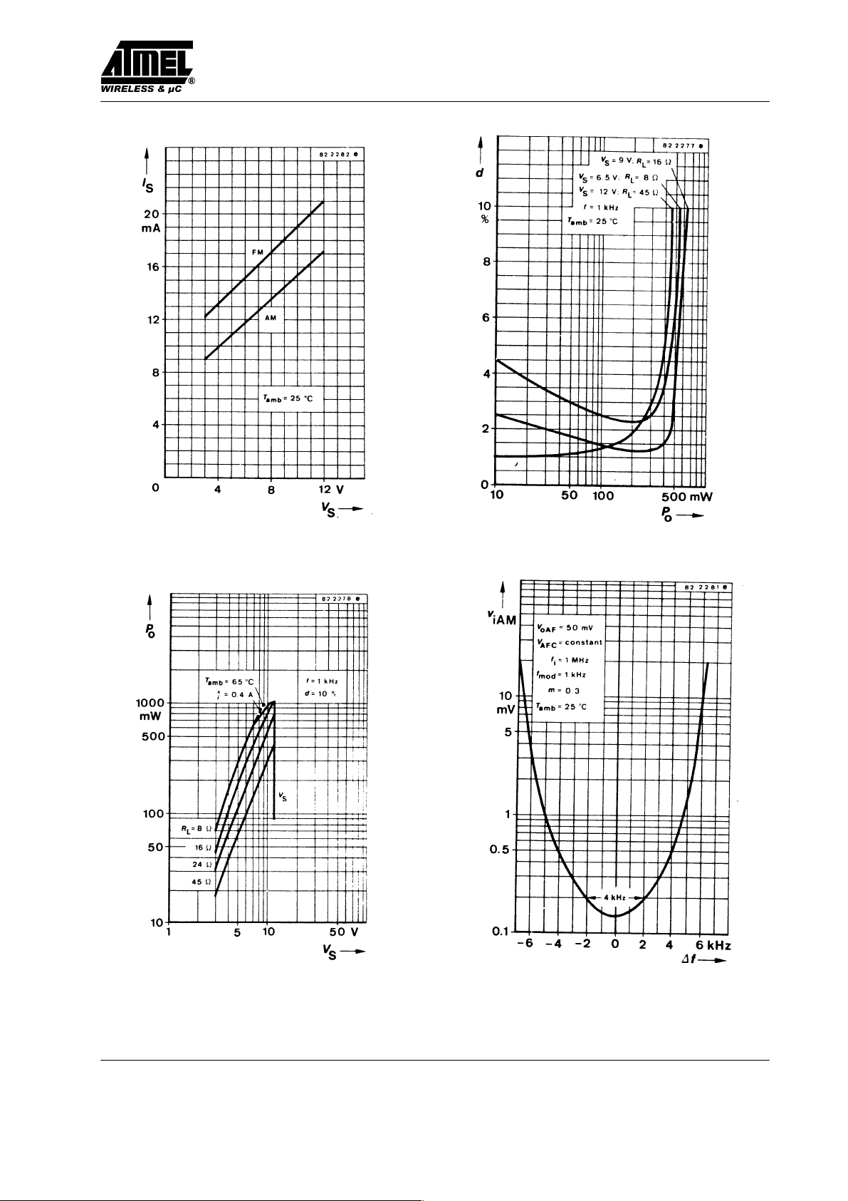
Figure 2.
Figure 4.
Figure 3.
Rev. A2, 23–Feb–01 3 (8)
Figure 5.

TDA1083
Figure 6.
Figure 7.
Rev. A2, 23–Feb–014 (8)

TDA1083
Figure 8.
Components in Figure 9
L
1
L
2
L
3
L
4
L
5
L
6
L
7
L
8
L
9
L
10
L
11
L
12
L
13
L
14
L
15
L
16
455 kHz = Ceramic filter LBF 6 (Componex) or CFU 445 H (Stettner)
10.7 MHz = Ceramic filter 10.7 MF–18 (Componex) or SFE 10.7 MA (Stettner)
Dr1, D
D
r2
D
r4
C6=C
C
19
C
21
R
8
= 4 Wdg ∅ 0.45 CuL, threaded core 7.5x3 material: Fi 01 U8 (Vogt GmbH)
= 5 Wdg ∅ 0.45 CuL
= 5 Wdg ∅ 0.45 CuL, air core ∅ 3.5 mm
= 3+3 Wdg ∅ 0.45 CuL, air core ∅ 2.7 mm
= 12 Wdg ∅ 0.25 CuL, Pin 3–1, filter kit 154 AN(C) or 154ANS–7 A6363A0 (TOKO, Componex)
= 2 Wdg ∅ 0.25 CuL, Pin 4–6
= 7 Wdg ∅ 0.25 CuL, Pin 6–3, filter kit 154AN(C) or 154EES–7 A6392FA (TOKO, Componex)
= 7 Wdg ∅ 0.16 CuL, Pin 1–4, filter kit 154AN(C) or 154EES–7 A6391ABM (TOKO, Componex)
= 5 Wdg ∅0.16 CuL, Pin 2–6
= 96 Wdg ∅ 0.25 CuLs, ferrite aerial ∅ 8x130 mm, type 031039–2103–606, (Draloric)
= 6 Wdg ∅ 0.25 CuLs
= 78 Wdg ∅ 0.09 CuL, Pin 3–4, filter kit RBR or RWOS–6A7609AAU (TOKO, Componex)
= 7 Wdg ∅ 0.09 CuL, Pin 2–1
= 18 Wdg ∅ 0.09 CuL, Pin 3–4, filter kit RHN(C) or RHCS–1A7607AQH (TOKO, Componex)
= 46+100 Wdg ∅ 0.09 CuL, Pin 6–2–1
= 72+72 Wdg ∅ 0.09 Cul Pin 3–4/6–1, filter kit RHN(C) or RHNS–1A7608AZP (TOKO, Componex)
= Ferrit bead on the transistor terminal
r3
= 16 Wdg ∅ 0.25 CuL, ∅ 2 air core
= 6 Wdg ∅ 0.15 CuL, ∅ 2.1x3 mm ferrit bead
= 4.5 to 20 pF, variable capacitor type CY2–22124–RT02 (TOKO, Componex)
14
= 5 to 80 pF
= 5 to 140 pF
= According to gain groups , 47 k or 33 k
Rev. A2, 23–Feb–01 5 (8)

TDA1083
Figure 9. FM-/AM-receiver circuit
Rev. A2, 23–Feb–016 (8)

TDA1083
Figure 10.
Package Information
Rev. A2, 23–Feb–01 7 (8)

TDA1083
Ozone Depleting Substances Policy Statement
It is the policy of Atmel Germany GmbH to
1. Meet all present and future national and international statutory requirements.
2. Regularly and continuously improve the performance of our products, processes, distribution and operating systems
with respect to their impact on the health and safety of our employees and the public, as well as their impact on
the environment.
It is particular concern to control or eliminate releases of those substances into the atmosphere which are known as
ozone depleting substances (ODSs).
The Montreal Protocol (1987) and its London Amendments (1990) intend to severely restrict the use of ODSs and forbid
their use within the next ten years. Various national and international initiatives are pressing for an earlier ban on these
substances.
Atmel Germany GmbH has been able to use its policy of continuous improvements to eliminate the use of ODSs listed
in the following documents.
1. Annex A, B and list of transitional substances of the Montreal Protocol and the London Amendments respectively
2. Class I and II ozone depleting substances in the Clean Air Act Amendments of 1990 by the Environmental
Protection Agency (EPA) in the USA
3. Council Decision 88/540/EEC and 91/690/EEC Annex A, B and C (transitional substances) respectively.
Atmel Germany GmbH can certify that our semiconductors are not manufactured with ozone depleting substances
and do not contain such substances.
We reserve the right to make changes to improve technical design and may do so without further notice.
Parameters can vary in different applications. All operating parameters must be validated for each customer
application by the customer. Should the buyer use Atmel Wireless & Microcontrollers products for any unintended
or unauthorized application, the buyer shall indemnify Atmel Wireless & Microcontrollers against all claims,
costs, damages, and expenses, arising out of, directly or indirectly, any claim of personal damage, injury or death
associated with such unintended or unauthorized use.
Data sheets can also be retrieved from the Internet: http://www.atmel–wm.com
Atmel Germany GmbH, P.O.B. 3535, D-74025 Heilbronn, Germany
Telephone: 49 (0)7131 67 2594, Fax number: 49 (0)7131 67 2423
Rev. A2, 23–Feb–018 (8)
 Loading...