

BDTIC www.bdtic.com/ATMEL
Features
• High Performance, Low Power AVR
• Advanced RISC Architecture
– 131 Powerful Instructions - Most Single Clock Cycle Execution
– 32 x 8 General Purpose Working Registers
– Fully Static Operation
– Up to 4 MIPS Throughput at 4 MHz
• High Endurance Non-volatile Memorie segments
– 8K/16K Bytes of In-System Self-Programmable Flash Program
Memory(A Tmega8HVA/16HVA)
– 256 Bytes EEPROM
– 512 Bytes Internal SRAM
– Write/Erase cycles: 10,000 Flash/100,000 EEPROM
– Data Retention: 20 years at 85°C /100 years at 25°C
– Programming Lock for Software Security
• Battery Management Features
– One or Two Cells in Series
– Over-current Protection (Charge and Discharge)
– Short-circuit Protection (Discharge)
– High Voltage Outputs to Drive N-Channel Charge/Discharge FETs
• Peripheral Features
– Two configurable 8- or 16-bit Timers with Separate Prescaler, Optional Input
Capture (IC), Compare Mode and CTC
– SPI - Serial Programmable Interface
– 12-bit Voltage ADC, Four External and One Internal ADC Inputs
– High Resolution Coulomb Counter ADC for Current Measurements
– Programmable Watchdog Timer
• Special Microcontroller Features
– debugWIRE On-chip Debug System
– In-System Programmable via SPI ports
– Power-on Reset
– On-chip Voltage Regulator with Short-circuit Monitoring Interface
– External and Internal Interrupt Sources
– Sleep Modes:
Idle, ADC Noise Reduction, Power-save, and Power-off
• Additional Secure Authentication Features available only under ND A
• Packages
– 36-pad LGA
– 28-lead TSOP
• Operating Voltage: 1.8 - 9V
• Maximum Withstand Voltage (High-voltage pins): 28V
• Temperature Range: - 20°C to 85°C
• Speed Grade: 1-4 MHz
®
8-bit Microcontroller
(1)
8-bit
Microcontroller
with 8K/16K
Bytes In-System
Programmable
Flash
ATmega8HVA
ATmega16HVA
Preliminary
Summary
8024AS–AVR–04/08
ATmega8HVA/16HVA
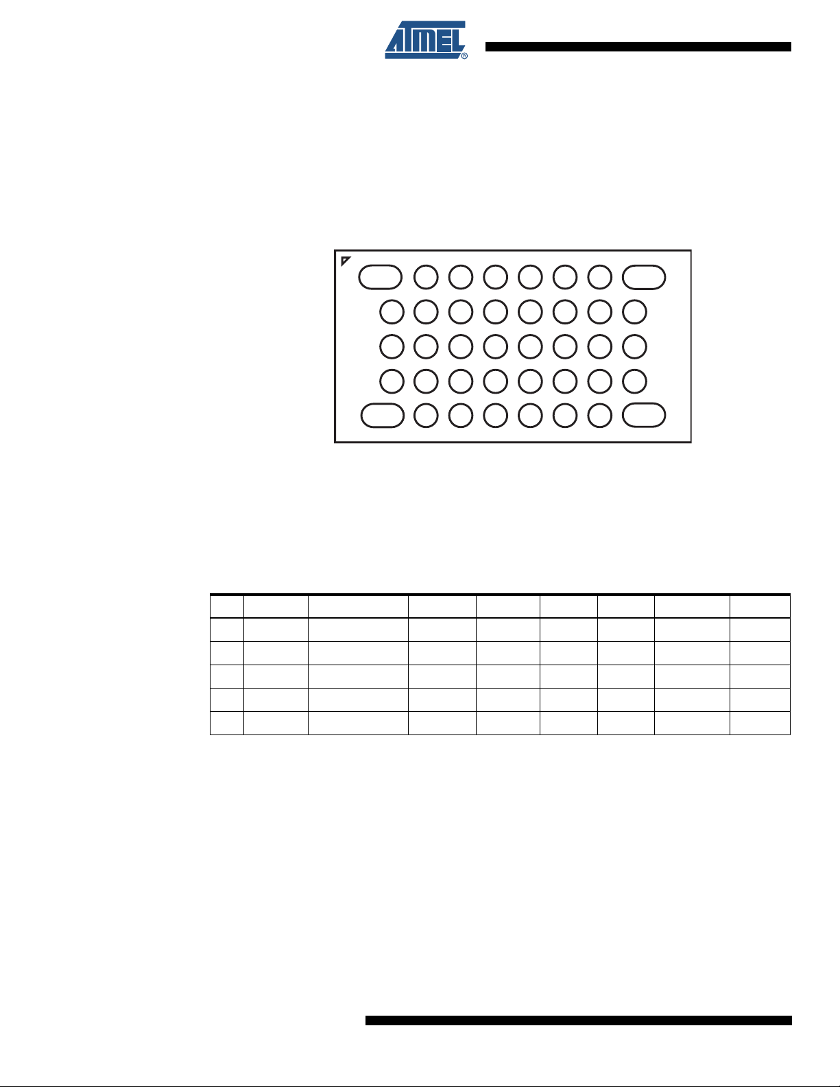
1. Pin Configurations
A
B
C
D
E
1.1 LGA
Figure 1-1. LGA - Pinout ATmega8HVA/16HVA
12345678
Figure 1-2. LGA - pinout ATmega8HVA/16HVA
12 3 4567 8
A DNC PV2 PV1 NV GND OC OD DNC
B CF2P CF2N VFET CF1P GND PC0 DNC GND
C VREF VREFGND VREG CF1N VCC GND GND BATT
DPI NI GND GND GND PB2 PB3 GND
E DNC DNC PA1 PA0 PB1 PB0 RESET DNC
2
8024AS–AVR–04/08

1.2 TSOP
V
0)
1)
)
ATmega8HVA/16HVA
Figure 1-3. TSOP - pinout ATmega8HVA/16HVA
1.3 Pin Descriptions
1
PV2
2
PV1
3
NV
GND
4
VFET
5
6
CF1P
CF1N
7
8
CF2P
CF2N
9
VREG
10
11
VREF
REFGND
12
13
PI
14 15
NI PA0 (ADC0/SGND/T
28
OD
27
OC
26
GND
25
BATT
24
PC0 (RXD/TXD/INT0
23
VCC
22
GND
21
PB3 (MISO/INT2)
20
PB2 (MOSI/INT1)
19
PB1 (SCK)
18
PB0 (SS/CKOUT)
17
PA2 (RESET/dW)
16
PA1 (ADC1/SGND/T
1.3.1 VFET
Input to the internal voltage regulator.
1.3.2 VCC
Digital supply voltage. Normally connected to VREG.
1.3.3 VREG
Output from the internal voltage regulator.
1.3.4 CF1P/CF1N/CF2P/CF2N
CF1P/CF1N/CF2P/CF2N are the connection pins for connecting external fly capacito rs to the
step-up regulator.
1.3.5 VREF
Internal Voltage Reference for external decoupling.
1.3.6 VREFGND
Ground for decoupling of Internal Voltage Reference. Do not conn ect t o GND or SGND on PCB.
8024AS–AVR–04/08
3

ATmega8HVA/16HVA
1.3.7 GND
Ground
1.3.8 Port A (PA1..PA0)
Port A serves as a low-voltage 2-bit bi-d irectional I/ O port with internal pull-up resisto rs (selected
for each bit). As inputs, Port A pins that are externally pulled low will source current if the pull-up
resistors are activated. The Port A pins are tri-stated when a reset co ndition becomes active,
even if the clock is not running.
Port A also serves the functions of various special features of the ATmega8HVA/16HVA as
listed in ”Alternate Functions of Port A” on page 70.
1.3.9 Port B (PB3..PB0)
Port B is a low-voltage 4-bit bi-directional I/O port with internal pull-up resistors (selected for
each bit). As inputs, Port B pins that are externally pulled low will source current if the pull-up
resistors are activated. The Port B pins are tri-stated when a reset co ndition becomes active,
even if the clock is not running.
Port B also serves the functions of various special features of the ATmega8HVA/16HVA as
listed in ”Alternate Functions of Port B” on page 71.
1.3.10 PC0
Port C serves the functions of various special features of the ATmega8HVA/16HVA as listed in
”Alternate Functions of Port C” on page 61.
1.3.11 OC
1.3.12 OD
1.3.13 NI
1.3.14 PI
1.3.15 NV/PV1/PV2
1.3.16 BATT
1.3.17 RESET
/dw
High voltage output to drive Charge FET.
High voltage output to drive Discharge FET.
NI is the filtered negative input from the current sense resistor.
PI is the filtered positive input from the current sense resistor.
NV, PV1, and PV2 are the inputs for battery cells 1 and 2.
Input for detecting when a charger is connected.
Reset input. A low level on this pin for longer than the minimum pulse length will generate a
reset, even if the clock is not running. The minimum pulse length is given in Table 11 on page
38. Shorter pulses are not guaranteed to generate a reset. This pin is also used as debugWIRE
communication pin.
4
8024AS–AVR–04/08
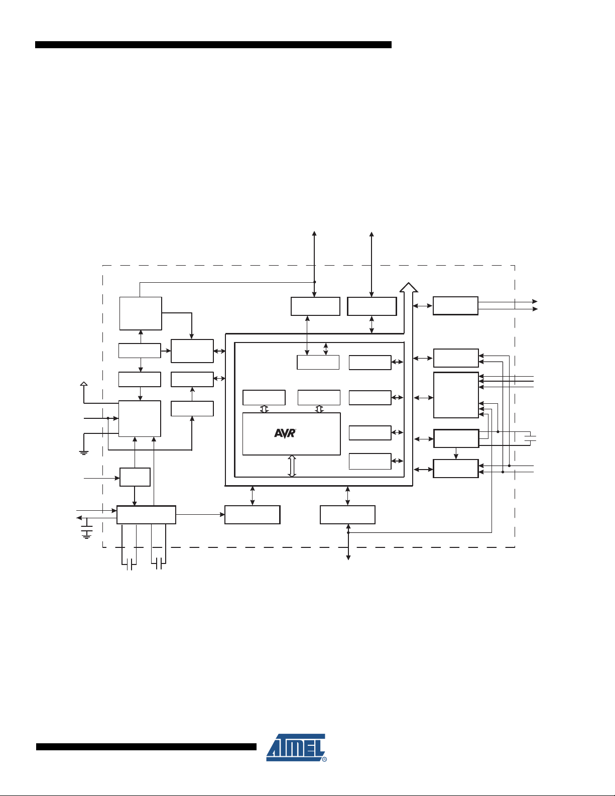
2. Overview
R
D
PB3..0
CF1P CF2P
PC0
The ATmega8HVA/16HVA is a monitoring and protection circuit for 1-cell and 2-cell Li-ion applications with focus on high security/authentication, accurate monitoring, low cost and high
utilization of the cell energy. The device contains secur e authentication features as well as
autonomous battery protection during charging and discharging. The chip allows very accurate
accumulated current measurements using an 18-bit ADC with a resolution of 0.84 µV. The feature set makes the ATmega8HVA/16HVA a key component in any system focusing on high
security, battery protection, accurate monitoring, high system utilization and low cost.
Figure 2-1. Block Diagram
ATmega8HVA/16HVA
PB0
ESET/dW
BATT
VFET
VREG
Oscillator
Circuits /
Clock
Generation
Watchdog
Oscillator
VCC
GND
CF1N CF2N
Watchdog
Timer
Power
Supervision
POR &
RESET
Charger
Detect
Voltage
Regulator
Oscillator
Sampling
Interface
Program
Logic
debugWIRE
Voltage Regulator
Monitor Interface
PORTB (4)
SPI
SRAMFlash
CPU
DATA BUS
8/16-bit T/C0
8/16-bit T/C1
PORTA (2)
PA1..0
PORTC (1)
EEPROM
Security
Module
Protection
Reference
Counter ADC
PA1..0
FET
Control
Battery
Voltage
ADC
Voltage
Coulumb
VPTAT
OC
OD
PV2
PV1
NV
VREF
VREFGN
PI
NI
A combined step-up and linear voltage regulator ensures that the chip can operate with supply
voltages as low as 1.8V for 1-cell applications. The regulator automatically switches to linear
mode when the input voltage is sufficiently high, thereby ensuring a minimum power consumption at all times. For 2-cell applications, only linear regulation is enabled. The regulator
capabilities, combined with an extremely low power consumption in the power saving modes,
greatly enhances the cell energy utilization compared to existing solutions.
The chip utilizes Atmel's patented Deep Under-voltage Recovery (DUVR) mode that supports
pre-charging of deeply discharged ba tt er y cells without using a separate Pre-charge FET.
5
8024AS–AVR–04/08

ATmega8HVA/16HVA
The ATmega8HVA/16HVA contains a 12-bit ADC that can be used to measure the voltage of
each cell individually. The ADC can also be used to monitor temperature, either on-chip temperature using the built-in temperature sensor, external t emper ature using thermi stors conne cted to
dedicated ADC inputs. The ATmega8HVA/16HVA contains a high-voltage tolerant, open-drain
IO pin that supports serial communication. Programming can be done in-system using the 4
General Purpose IO ports that support SPI programming.
The AVR core combines a rich instruction set with 32 general purpose working registers. All the
32 registers are directly connected to the Arithmetic Logic Unit (ALU), allowing two independent
registers to be accessed in one single instruction executed in one clock cycle. The resulting
architecture is more code efficient while achieving throughputs up to ten times faster than conventional CISC microcontrollers.
The MCU includes 8K/16K bytes of In-System Programmable Flash with Re ad-While-Write
capabilities, 256 bytes EEPROM, 512 bytes SRAM, 32 general purpose working registers, 6
general purpose I/O lines, debugWIRE for On-chip debugging and SPI for In-system Programming, two flexible Timer/Counters with Input Capture and compare modes, internal and external
interrupts, a 12-bit Sigma Delta ADC for voltage and temperature measurements, a high resolution Sigma Delta ADC for Coulomb Counting and instantan eous current measurements,
Additional Secure Authentication Features, an authonomou s Battery Protection module, a pro grammable Watchdog Timer with wake-up capabilities, and software selectable power saving
modes.
The AVR core combines a rich instruction set with 32 general purpose working registers. All the
32 registers are directly connected to the Arithmetic Logic Unit (ALU), allowing two indepdent
registers to be accessed in one single instruction executed in one clock cycle. The resulting
architecture is more code efficient while achieving throughputs up to ten times faster than conventional CISC microcontrollers.
The device is manufactured using Atmel’s high voltage high density non-volatile memo ry technology. The On-chip ISP Flash allows the program memory to be reprogrammed In-System,
through an SPI serial interface, by a conven tional no n-volatile memory progr ammer or by a n Onchip Boot program running on the AVR core. By com bining an 8-bit RISC CPU with In-System
Self-Programmable Flash, fuel gauging ADCs, dedicated battery protection circuitry, and a voltage regulator on a monolithic chip, the ATmega8HVA/16HVA is a powerful microcontroller that
provides a highly flexible and cost effective solution for Li-ion Smart Battery applications.
The ATmega8HVA/16HVA AVR is supported with a full suite of program and system development tools including: C Compilers, Macro Assemblers, Program Debugger/Simulators, and Onchip Debugger.
The ATmega8HVA/16HVA is a low-power CMOS 8-bit microcontroller based on the AVR architecture. It is part of the AVR Smart Battery family that provides secure authentication, highly
accurate monitoring and autonomous protection for Lithium-ion battery cells.
6
8024AS–AVR–04/08
2.1 Comparison Between ATmega8HVA and ATmega16HVA
The ATmega8HVA and ATmega16HVA differ only in memory size and interrupt vector size.
Table 2-1 summarizes the different configuration for the two devices.
Table 2-1. Configuration summary
Device Flash Interrupt vector size
ATmega8HVA 8K 1 Word
ATmega16HVA 16K 2 Word
3. Disclaimer
All Min, Typ and Max values contained in this datasheet are preliminary estimat es based on simulations and characterization of other AVR microcontrollers manufactured on the same process
technology. Final values will be available after the device is characterized.
4. Resources
A comprehensive set of development tools, application notes and datasheets are available for
download on http://www.atmel.com/avr.
ATmega8HVA/16HVA
5. Data Retention
Note: 1.
Reliability Qualification results show that the projected data retention failure rate is much less
than 1 PPM over 20 years at 85°C or 100 years at 25°C.
8024AS–AVR–04/08
7

ATmega8HVA/16HVA
6. Register Summary
Address Name Bit 7 Bit 6 Bit 5 Bit 4 Bit 3 Bit 2 Bit 1 Bit 0 Page
(0xFF) Reserved – – – – – – – –
(0xFE) BPPLR – – – – – – BPPLE BPPL 127
(0xFD) BPCR – – – SCD DOCD COCD DHCD CHCD 127
(0xFC) BPHCTR – – HCPT[5:0] 130
(0xFB) BPOCTR – – OCPT[5:0] 129
(0xFA) BPSCTR – SCPT[6:0] 128
(0xF9) BPCHCD CHCDL[7:0] 132
(0xF8) BPDHCD DHCDL[7:0] 132
(0xF7) BPCOCD COCDL[7:0] 131
(0xF6) BPDOCD DOCDL[7:0] 131
(0xF5) BPSCD SCDL[7:0] 131
(0xF4) Reserved – – – – – – – –
(0xF3) BPIFR – – – SCIF DOCIF COCIF DHCIF CHCIF 134
(0xF2) BPIMSK – – – SCIE DOCIE COCIE DHCIE CHCIE 133
(0xF1) Reserved
(0xF0) FCSR
(0xEF) Reserved – – – – – – – –
(0xEE) Reserved
(0xED) Reserved
(0xEC) Reserved – – – – – – – –
(0xEB) Reserved – – – – – – – –
(0xEA) Reserved – – – – – – – –
(0xE9) CADICH CADIC[15:8] 110
(0xE8) CADICL CADIC[7:0] 110
(0xE7) Reserved – – – – – – – –
(0xE6) CADRC CADRC[7:0] 111
(0xE5) CADCSRB – CADACIE – CADICIE – CADACIF CADRCIF CADICIF 109
(0xE4) CADCSRA CADEN CADPOL CADUB CADAS[1:0] CADSI[1:0] CADSE 107
(0xE3) CADAC3 CADAC[31:24] 110
(0xE2) CADAC2 CADAC[23:16] 110
(0xE1) CADAC1 CADAC[15:8] 110
(0xE0) CADAC0 CADAC[7:0] 110
(0xDF) Reserved – – – – – – – –
(0xDE) Reserved – – – – – – – –
(0xDD) Reserved – – – – – – – –
(0xDC) Reserved – – – – – – – –
(0xDB) Reserved – – – – – – – –
(0xDA) Reserved – – – – – – – –
(0xD9) Reserved – – – – – – – –
(0xD8) Reserved – – – – – – – –
(0xD7) Reserved – – – – – – – –
(0xD6) Reserved
(0xD5) Reserved
(0xD4) Reserved – – – – – – – –
(0xD3) Reserved
(0xD2) Reserved
(0xD1) BGCRR BGCR[7:0] 119
(0xD0) BGCCR BGD
(0xCF) Reserved
(0xCE) Reserved
(0xCD) Reserved – – – – – – – –
(0xCC) Reserved
(0xCB) Reserved
(0xCA) Reserved – – – – – – – –
(0xC9) Reserved
(0xC8) ROCR ROCS
(0xC7) Reserved – – – – – – – –
(0xC6) Reserved
(0xC5) Reserved – – – – – – – –
(0xC4) Reserved
(0xC3)
(0xC2) Reserved – – – – – – – –
(0xC1) Reserved
(0xC0) Reserved
Reserved
– – – – – – – –
– – – – DUVRD CPS DFE CFE 138
– – – – – – – –
– – – – – – – –
– – – – – – – –
– – – – – – – –
– – – – – – – –
– – – – – – – –
– BGCC[5:0] 118
– – – – – – – –
– – – – – – – –
– – – – – – – –
– – – – – – – –
– – – – – – – –
– – – – – ROCWIF ROCWIE 123
– – – – – – – –
– – – – – – – –
– – – – – – – –
– – – – – – – –
– – – – – – – –
8
8024AS–AVR–04/08

ATmega8HVA/16HVA
Address Name Bit 7 Bit 6 Bit 5 Bit 4 Bit 3 Bit 2 Bit 1 Bit 0 Page
(0xBF) Reserved – – – – – – – –
(0xBE) Reserved – – – – – – – –
(0xBD) Reserved – – – – – – – –
(0xBC) Reserved – – – – – – – –
(0xBB) Reserved – – – – – – – –
(0xBA) Reserved
(0xB9) Reserved
(0xB8) Reserved – – – – – – – –
(0xB7) Reserved – – – – – – –
(0xB6) Reserved – – – – – – – –
(0xB5) Reserved – – – – – – – –
(0xB4) Reserved – – – – – – – –
(0xB3) Reserved – – – – – – – –
(0xB2) Reserved – – – – – – – –
(0xB1) Reserved – – – – – – – –
(0xB0) Reserved – – – – – – – –
(0xAF) Reserved – – – – – – – –
(0xAE) Reserved
(0xAD) Reserved
(0xAC) Reserved – – – – – – – –
(0xAB) Reserved – – – – – – – –
(0xAA) Reserved – – – – – – – –
(0xA9) Reserved – – – – – – – –
(0xA8) Reserved – – – – – – – –
(0xA7) Reserved – – – – – – – –
(0xA6) Reserved – – – – – – – –
(0xA5) Reserved – – – – – – – –
(0xA4) Reserved – – – – – – – –
(0xA3) Reserved – – – – – – – –
(0xA2) Reserved – – – – – – – –
(0xA1) Reserved – – – – – – – –
(0xA0) Reserved – – – – – – – –
(0x9F) Reserved – – – – – – – –
(0x9E) Reserved – – – – – – – –
(0x9D) Reserved – – – – – – – –
(0x9C) Reserved – – – – – – – –
(0x9B) Reserved – – – – – – – –
(0x9A) Reserved – – – – – – – –
(0x99) Reserved – – – – – – – –
(0x98) Reserved – – – – – – – –
(0x97) Reserved – – – – – – – –
(0x96) Reserved – – – – – – – –
(0x95) Reserved – – – – – – – –
(0x94) Reserved – – – – – – – –
(0x93) Reserved
(0x92) Reserved
(0x91) Reserved – – – – – – – –
(0x90) Reserved
(0x8F) Reserved
(0x8E) Reserved
(0x8D) Reserved – – – – – – – –
(0x8C) Reserved
(0x8B) Reserved
(0x8A) Reserved – – – – – – – –
(0x89) OCR1B Timer/Counter1 – Output Compare Register B 92
(0x88) OCR1A Timer/Counter1 – Output Compare Register A 91
(0x87) Reserved – – – – – – – –
(0x86) Reserved
(0x85) TCNT1H Timer/Counter1 (8 Bit) High Byte 91
(0x84) TCNT1L Timer/Counter1 (8 Bit) Low Byte 91
(0x83) Reserved – – – – – – – –
(0x82) Reserved – – – – – – – –
(0x81) TCCR1B
(0x80) TCCR1A TCW1 ICEN1 ICNC1 ICES1 ICS1
(0x7F) Reserved – – – – – – – –
(0x7E) DIDR0
– – – – – – – –
– – – – – – – –
– – – – – – – –
– – – – – – – –
– – – – – – – –
– – – – – – – –
– – – – – – – –
– – – – – – – –
– – – – – – – –
– – – – – – – –
– – – – – – – –
– – – – – – – –
– – – – – CS12 CS11 CS10 76
– –WGM10 90
– – – – – – PA1DID PA0DID 116
8024AS–AVR–04/08
9

ATmega8HVA/16HVA
Address Name Bit 7 Bit 6 Bit 5 Bit 4 Bit 3 Bit 2 Bit 1 Bit 0 Page
(0x7D) Reserved – – – – – – – –
(0x7C) VADMUX – – – – VADMUX[3:0] 114
(0x7B) Reserved – – – – – – – –
(0x7A) VADCSR – – – – VADEN VADSC VADCCIF VADCCIE 114
(0x79) VADCH – – – – VADC Data Register High byte 115
(0x78) VADCL VADC Data Register Low byte 115
(0x77) Reserved – – – – – – – –
(0x76) Reserved – – – – – – – –
(0x75) Reserved – – – – – – – –
(0x74) Reserved – – – – – – – –
(0x73) Reserved – – – – – – – –
(0x72) Reserved – – – – – – – –
(0x71) Reserved – – – – – – – –
(0x70) Reserved – – – – – – – –
(0x6F) TIMSK1 – – – – ICIE1 OCIE1B OCIE1A TOIE1 92
(0x6E) TIMSK0 – – – – ICIE0 OCIE0B OCIE0A TOIE0 92
(0x6D) Reserved – – – – – – – –
(0x6C) Reserved
(0x6B) Reserved
(0x6A) Reserved – – – – – – – –
(0x69) EICRA – – ISC21 ISC20 ISC11 ISC10 ISC01 ISC00 56
(0x68) Reserved – – – – – – – –
(0x67) Reserved – – – – – – – –
(0x66) FOSCCAL Fast Oscillator Calibration Re gister 30
(0x65) Reserved – – – – – – – –
(0x64) PRR0 – – PRVRM – PRSPI PRTIM1 PRTIM0 PRVADC 39
(0x63) Reserved – – – – – – – –
(0x62) Reserved – – – – – – – –
(0x61) CLKPR CLKPCE – – – – – CLKPS1 CLKPS0 31
(0x60) WDTCSR WDIF WDIE WDP3 WDCE WDE WDP2 WDP1 WDP0 49
0x3F (0x5F) SREG I T H S V N Z C 9
0x3E (0x5E) SPH SP15 SP14 SP13 SP12 SP11 SP10 SP9 SP8 12
0x3D (0x5D) SPL SP7 SP6 SP5 SP4 SP3 SP2 SP1 SP0 12
0x3C (0x5C) Reserved – – – – – – – –
0x3B (0x5B) Reserved – – – – – – – –
0x3A (0x5A) Reserved – – – – – – – –
0x39 (0x59) Reserved – – – – – – – –
0x38 (0x58) Reserved – – – – – – – –
0x37 (0x57) SPMCSR – – SIGRD CTPB RFLB PGWRT PGERS SPMEN 147
0x36 (0x56) Reserved – – – – – – – –
0x35 (0x55) MCUCR – –CKOEPUD – – – – 73/31
0x34 (0x54) MCUSR – – – OCDRF WDRF BODRF EXTRF PORF 49
0x33 (0x53) SMCR – – – – SM[2:0] SE 39
0x32 (0x52) Reserved – – – – – – – –
0x31 (0x51) DWDR debugWIRE Data Register 140
0x30 (0x50) Reserved – – – – – – – –
0x2F (0x4F) Reserved – – – – – – – –
0x2E (0x4E) SPDR SPI Data Register 103
0x2D (0x4D) SPSR SPIF WCOL – – – – –SPI2X 102
0x2C (0x4C) SPCR SPIE SPE DORD MSTR CPOL CPHA SPR1 SPR0 101
0x2B (0x4B) GPIOR2 General Purpose I/O Register 2 23
0x2A (0x4A) GPIOR1 General Purpose I/O Register 1 23
0x29 (0x49) OCR0B Timer/Counter0 Output Compare Register B 92
0x28 (0x48) OCR0A Timer/Counter0 Output Compare Register A 91
0x27 (0x47) TCNT0H Timer/Counter0 (8 Bit) High Byte 91
0x26 (0x46) TCNT0L Timer/Counter0 (8 Bit) Low Byte 91
0x25 (0x45) TCCR0B
0x24 (0x44) TCCR0A TCW0 ICEN0 ICNC0 ICES0 ICS0
0x23 (0x43) GTCCR TSM
0x22 (0x42) Reserved – – – – – – – –
0x21 (0x41) EEAR EEPROM Address Register Low Byte 19
0x20 (0x40) EEDR EEPROM Data Register 19
0x1F (0x3F) EECR – – EEPM1 EEPM0 EERIE EEMPE EEPE EERE 19
0x1E (0x3E) GPIOR0 General Purpose I/O Register 0 23
0x1D (0x3D) EIMSK
0x1C (0x3C) EIFR
– – – – – – – –
– – – – – – – –
– – – – – CS02 CS01 CS00 76
– –WGM00 90
– – – – – – PSRSYNC
– – – – – INT2 INT1 INT0 57
– – – – – INTF2 INTF1 INTF0 57
10
8024AS–AVR–04/08

ATmega8HVA/16HVA
Address Name Bit 7 Bit 6 Bit 5 Bit 4 Bit 3 Bit 2 Bit 1 Bit 0 Page
0x1B (0x3B) Reserved – – – – – – – –
0x1A (0x3A) Reserved – – – – – – – –
0x19 (0x39) Reserved – – – – – – – –
0x18 (0x38) Reserved – – – – – – – –
0x17 (0x37) OSICSR – – – OSISEL0 – – OSIST OSIEN 32
0x16 (0x36) TIFR1
0x15 (0x35) TIFR0
0x14 (0x34) Reserved – – – – – – – –
0x13 (0x33) Reserved – – – – – – – –
0x12 (0x32) Reserved – – – – – – – –
0x11 (0x31) Reserved – – – – – – – –
0x10 (0x30) Reserved – – – – – – – –
0x0F (0x2F) Reserved – – – – – – – –
0x0E (0x2E) Reserved – – – – – – – –
0x0D (0x2D) Reserved – – – – – – – –
0x0C (0x2C) Reserved – – – – – – – –
0x0B (0x2B) Reserved – – – – – – – –
0x0A (0x2A) Reserved
0x09 (0x29) Reserved
0x08 (0x28) PORTC – – – – – – –PORTC0 62
0x07 (0x27) Reserved – – – – – – – –
0x06 (0x26) PINC – – – – – – – PINC0 62
0x05 (0x25) PORTB – – – – PORTB3 PORTB2 PORTB1 PORTB0 73
0x04 (0x24) DDRB – – – – DDB3 DDB2 DDB1 DDB0 73
0x03 (0x23) PINB – – – – PINB3 PINB2 PINB1 PINB0 73
0x02 (0x22) PORTA – – – – – – PORTA1 PORTA0 73
0x01 (0x21) DDRA – – – – – – DDA1 DDA0 73
0x00 (0x20) PINA – – – – – –PINA1PINA0 73
Notes: 1. For compatibility with future devices, reserved bits should be written to zero if accessed. Reserved I/O memory addresses
should never be written.
2. I/O registers within the address range $00 - $1F are directly bit-accessible using the SBI and CBI instructions. In these registers, the value of single bits can be checked by using the SBIS and SBIC instructions.
3. Some of the status flags are cleared by writing a logical one to them. Note that the CBI and SBI instructions will operate on
all bits in the I/O register, writing a one back into any flag read as set, thus clearing the flag. The CBI and SBI instructions
work with registers 0x00 to 0x1F on ly.
4. When using the I/O specific commands IN and OUT, the I/O addresses $00 - $3F must be used. When addressing I/O registers as data space using LD and ST instructions, $20 must be added to these addresses. The ATmega8HVA/16HVA is a
complex microcontroller with more peripheral units than can be supported within the 64 location reserved in Opcode for the
IN and OUT instructions. For the Extended I/O space from $60 - $FF in SRAM, only the ST/STS/STD and LD/LDS/LDD
instructions can be used.
– – – – ICF1 OCF1B OCF1A TOV1 93
– – – – ICF0 OCF0B OCF0A TOV0 93
– – – – – – – –
– – – – – – – –
8024AS–AVR–04/08
11
ATmega8HVA/16HVA
7. Instruction Set Summary
Mnemonics Operands Description Operation Flags #Clocks
ARITHMETIC AND LOGIC INSTRUCTIONS
ADD Rd, Rr Add two Registers Rd ← Rd + Rr Z,C,N,V,H 1
ADC Rd, Rr Add with Carry two Registers Rd ← Rd + Rr + C Z,C,N,V,H 1
ADIW Rdl,K Add Immediate to Word Rdh:Rdl ← Rdh:Rdl + K Z,C,N,V,S 2
SUB Rd, Rr Subtract two Registers Rd ← Rd - Rr Z,C,N,V,H 1
SUBI Rd, K Subtract Constant from Register Rd ← Rd - K Z,C,N,V,H 1
SBC Rd, Rr Subtract with Carry two Registers Rd ← Rd - Rr - C Z,C,N,V,H 1
SBCI Rd, K Subtract with Carry Constant from Reg. Rd ← Rd - K - C Z,C,N,V,H 1
SBIW Rdl,K Subtract Immediate from Word Rdh:Rdl ← Rdh:Rdl - K Z,C,N,V,S 2
AND Rd, Rr Logical AND Registers Rd ← Rd • Rr Z,N,V 1
ANDI Rd, K Logical AND Register and Constant Rd ← Rd • K Z,N,V 1
OR Rd, Rr Logical OR Registers Rd ← Rd v Rr Z,N,V 1
ORI Rd, K Logical OR Register and Constant Rd ← Rd v K Z,N,V 1
EOR Rd, Rr Exclusive OR Registers Rd ← Rd ⊕ Rr Z,N,V 1
COM Rd One’s Complement Rd ← 0xFF − Rd Z,C,N,V 1
NEG Rd Two’s Complement Rd ← 0x00 − Rd Z,C,N,V,H 1
SBR Rd,K Set Bit(s) in Register Rd ← Rd v K Z,N,V 1
CBR Rd,K Clear Bit(s) in Register Rd ← Rd • (0xFF - K) Z,N,V 1
INC Rd Increment Rd ← Rd + 1 Z,N,V 1
DEC Rd Decrement Rd ← Rd − 1 Z,N,V 1
TST Rd Test for Zero or Minus Rd ← Rd • Rd Z,N,V 1
CLR Rd Clear Register Rd ← Rd ⊕ Rd Z,N,V 1
SER Rd Set Register Rd ← 0xFF None 1
MUL Rd, Rr Multiply Unsigned R1:R0 ← Rd x Rr Z,C 2
MULS Rd, Rr Multiply Signed R1:R0 ← Rd x Rr Z,C 2
MULSU Rd, Rr Multiply Signed with Unsigned R1:R0 ← Rd x Rr Z,C 2
FMUL Rd, Rr Fractional Multiply Unsigned R1:R0 ← (Rd x Rr) << 1 Z,C 2
FMULS Rd, Rr Fractional Multiply Signed R1:R0 ← (Rd x Rr) << 1 Z,C 2
FMULSU Rd, Rr Fractional Multiply Signed with Unsigned R1:R0 ← (Rd x Rr) << 1 Z,C 2
BRANCH INSTRUCTIONS
RJMP k Relative Jump PC ← PC + k + 1 None 2
IJMP Indirect Jump to (Z) PC ← Z None 2
(1)
JMP
RCALL k Relative Subroutine Call PC ← PC + k + 1 None 3
ICALL Indirect Call to (Z) PC ← ZNone3
(1)
CALL
RET Subroutine Return PC ← STACK None 4
RETI Interrupt Return PC ← STACK I 4
CPSE Rd,Rr Compare, Skip if Equal if (Rd = Rr) PC ← PC + 2 or 3 None 1/2/3
CP Rd,Rr Compare Rd − Rr Z, N,V,C,H 1
CPC Rd,Rr Compare with Carry Rd − Rr − C Z, N,V,C,H 1
CPI Rd,K Compare Reg i ster with Immediate Rd − K Z, N,V,C,H 1
SBRC Rr, b Skip if Bit in Register Cleared if (Rr(b)=0) PC ← PC + 2 or 3 None 1/2/3
SBRS Rr, b Skip if Bit in Register is Set if (Rr(b)=1) PC ← PC + 2 or 3 None 1/2/3
SBIC P, b Skip if Bit in I/O Register Cleared if (P(b)=0) PC ← PC + 2 or 3 None 1/2/3
SBIS P, b Skip if Bit in I/O Register is Set if (P(b)=1) PC ← PC + 2 or 3 None 1/2/3
BRBS s, k Branch if Status Flag Set if (SREG(s) = 1) then PC←PC+k + 1 None 1/2
BRBC s , k Branch if Sta tus Flag Cleared if (SREG(s) = 0) then PC←PC+k + 1 None 1/2
BREQ k Branch if Equal if (Z = 1) then PC ← PC + k + 1 None 1/2
BRNE k Branch if Not Equal if (Z = 0) then PC ← PC + k + 1 None 1/2
BRCS k Branch if Carry Set if (C = 1) then PC ← PC + k + 1 None 1/2
BRCC k Branch if Carry Cleared if (C = 0) then PC ← PC + k + 1 None 1/2
BRSH k Branch if Same or Higher if (C = 0) then PC ← PC + k + 1 None 1/2
BRLO k Branch if Lower if (C = 1) then PC ← PC + k + 1 None 1/2
BRMI k Branch if Minus if (N = 1) then PC ← PC + k + 1 None 1/2
BRPL k Branch if Plus if (N = 0) then PC ← PC + k + 1 None 1/2
BRGE k Branch if Greater or Equal, Signed if (N ⊕ V= 0) then PC ← PC + k + 1 None 1/ 2
BRLT k Branch if Less Than Zero, Signed if (N ⊕ V= 1) then PC ← PC + k + 1 None 1/2
BRHS k Branch if Half Carry Flag Set if (H = 1) then PC ← PC + k + 1 None 1/2
BRHC k Branch if Half Carry Flag Cleared if (H = 0) then PC ← PC + k + 1 None 1/2
BRTS k Branch if T Flag Set if (T = 1) then PC ← PC + k + 1 None 1/2
BRTC k Branch if T Flag Cleared if (T = 0) then PC ← PC + k + 1 None 1/2
BRVS k Branch if Overflow Flag is Set if (V = 1) then PC ← PC + k + 1 N one 1/2
BRVC k Branch if Overflow Flag is Cleared if (V = 0) then PC ← PC + k + 1 None 1/2
k Direct Jump PC ← kNone3
k Direct Subroutine Call PC ← kNone4
12
8024AS–AVR–04/08

ATmega8HVA/16HVA
7. Instruction Set Summary (Continued)
Mnemonics Operands Description Operation Flags #Clocks
BRIE k Branch if Interrupt Enabled if ( I = 1) then PC ← PC + k + 1 None 1/2
BRID k Branch if Interrupt Disabled if ( I = 0) then PC ← PC + k + 1 None 1/2
BIT AND BIT-TEST INSTRUCTIONS
SBI P,b Set Bit in I/O Register I/O(P,b) ← 1None2
CBI P,b Clear Bit in I/O Register I/O(P,b) ← 0None2
LSL Rd Logical Shift Left Rd(n+1) ← Rd(n), Rd(0) ← 0 Z,C,N,V 1
LSR Rd Logical Shift Right Rd(n) ← Rd(n+1), Rd(7) ← 0 Z,C,N,V 1
ROL Rd Rotate Left Through Carry Rd(0)←C,Rd(n+1)← Rd(n),C←Rd(7) Z,C,N,V 1
ROR Rd Rotate Right Through Carry Rd(7)←C,Rd(n)← Rd(n+1),C←Rd(0) Z,C,N,V 1
ASR Rd Arithmetic Shift Right Rd(n) ← Rd(n+1), n=0..6 Z,C,N,V 1
SWAP Rd Swap Nibbles Rd(3..0)← Rd(7..4),Rd(7..4)←Rd(3..0) None 1
BSET s Flag Set SREG(s) ← 1 SREG(s) 1
BCLR s Flag Clear SREG(s) ← 0 SREG(s) 1
BST Rr, b Bit Store from Register to T T ← Rr(b) T 1
BLD Rd, b Bit load from T to Register Rd(b) ← TNone1
SEC Set Carry C ← 1C1
CLC Clear Carry C ← 0 C 1
SEN Set Negative Flag N ← 1N1
CLN Clear Negative Flag N ← 0 N 1
SEZ Set Zero Flag Z ← 1Z1
CLZ Clear Zero Flag Z ← 0 Z 1
SEI Glo ba l Interru pt Ena ble I ← 1I1
CLI Global Interrupt Disable I ← 0 I 1
SES Set Signed Test Flag S ← 1S1
CLS Clear Signed Test Flag S ← 0 S 1
SEV Set Twos Complement Overflow. V ← 1V1
CLV Clear Twos Complement Overflow V ← 0 V 1
SET Set T in SREG T ← 1T1
CLT Clear T in SREG T ← 0 T 1
SEH Set Half Carry Flag in SREG H ← 1H1
CLH Clear Half Carry Flag in SREG H ← 0 H 1
DATA TRANSFER INSTRUCTIONS
MOV Rd, Rr Move Between Registers Rd ← Rr None 1
MOVW Rd, Rr Copy Register Word
LDI Rd, K Load Immediate Rd ← KNone1
LD Rd, X Load Indirect Rd ← (X) None 2
LD Rd, X+ Load Indirect and Post-Inc. Rd ← (X), X ← X + 1 None 2
LD Rd, - X Load Indirect and Pre-Dec. X ← X - 1, Rd ← (X) None 2
LD Rd, Y Load Indirect Rd ← (Y) None 2
LD Rd, Y+ Load Indirect and Post-Inc. Rd ← (Y), Y ← Y + 1 None 2
LD Rd, - Y Load Indirect and Pre-Dec. Y ← Y - 1, Rd ← (Y) None 2
LDD Rd,Y+q Load Indirect with Displacement Rd ← (Y + q) None 2
LD Rd, Z Load Indirect Rd ← (Z) None 2
LD Rd, Z+ Load Indirect and Post-Inc. Rd ← (Z), Z ← Z+1 None 2
LD Rd, -Z Load Indirect and Pre-Dec. Z ← Z - 1, Rd ← (Z) None 2
LDD Rd, Z+q Load Indirect with Displacement Rd ← (Z + q) None 2
LDS Rd, k Load Direct from SRAM Rd ← (k) None 2
ST X, Rr Store Indirect (X) ← Rr None 2
ST X+, Rr Store Indirect and Post-Inc. (X) ← Rr, X ← X + 1 None 2
ST - X, Rr Store Indirect and Pre-Dec. X ← X - 1, (X) ← Rr None 2
ST Y, Rr Store Indirect (Y) ← Rr No ne 2
ST Y+, Rr Store Indirect and Post-Inc. (Y) ← Rr, Y ← Y + 1 None 2
ST - Y, Rr Store Indirect and Pre-Dec. Y ← Y - 1, (Y) ← Rr None 2
STD Y+q,Rr Store Indirect with Displacement (Y + q) ← Rr None 2
ST Z, Rr Store Indirect (Z) ← Rr None 2
ST Z+, Rr Store Indirect and Post-Inc. (Z) ← Rr, Z ←
ST -Z, Rr Store Indirect and Pre-Dec. Z ← Z - 1, (Z) ← Rr None 2
STD Z+q,Rr Store Indirect with Displacement (Z + q) ← Rr None 2
STS k, Rr Store Direct to SRAM (k) ← Rr None 2
LPM Load Program Memory R0 ← (Z) None 3
LPM Rd, Z Load Program Memory Rd ← (Z) None 3
LPM Rd, Z+ Load Program Memo ry and Post-Inc Rd ← (Z), Z ← Z+1 None 3
SPM Store Program Memory (Z) ← R1:R0 None IN Rd, P In Port Rd ← PNone1
Rd+1:Rd ← Rr+1:Rr
Z + 1 None 2
None 1
8024AS–AVR–04/08
13

ATmega8HVA/16HVA
7. Instruction Set Summary (Continued)
Mnemonics Operands Description Operation Flags #Clocks
OUT P, Rr Out Port P ← Rr None 1
PUSH Rr Push Register on Stack STACK ← Rr None 2
POP Rd Pop Register from Stack Rd ← STACK None 2
MCU CONTROL INSTRUCTIONS
NOP No Operation None 1
SLEEP Sleep (see specific descr. for Sleep function) None 1
WDR Watchdog Reset (see specific descr. for WDR/timer) None 1
BREAK Break For On-chip Debug Only None N/A
Note: 1. These instructions are only available in ATmega16HVA.
14
8024AS–AVR–04/08

8. Ordering Information
8.1 ATmega8HVA
ATmega8HVA/16HVA
36CK1
28T
(1)
Operation Range
-20 to +85°C
Speed (MHz) Power Supply Ordering Code Package
1 - 4 1.8 - 9.0V
Notes: 1. Pb-free packaging, complies with the European Directive for Restriction of Hazardous Substances (RoHS directive). Also
Halide free and fully Green.
ATmega8HVA-4CKU
ATmega8HVA-4TU
Package Type
36CK1 36-pad, (6.50 x 3.50 x 0.85 mm Body, 0.60 mm Pitch), Land Grid Array (LGA) Package.
28T 28-lead (8 x 13.4 mm) Plastic Thin Small Outline Package, Type I (TSOP)
8024AS–AVR–04/08
15

ATmega8HVA/16HVA
8.2 ATmega16HVA
36CK1
28T
(1)
Operation Range
-20 to +85°C
Speed (MHz) Power Supply Ordering Code Package
1 - 4 1.8 - 9.0V
Notes: 1. Pb-free packaging, complies with the European Directive for Restriction of Hazardous Substances (RoHS directive). Also
Halide free and fully Green.
ATmega16HVA-4CKU
ATmega16HVA-4TU
36CK1 36-pad, (6.50 x 3.50 x 0.85 mm Body, 0.60 mm Pitch), Land Grid Array (LGA) Package.
28T 28-lead (8 x 13.4 mm) Plastic Thin Small Outline Package, Type I (TSOP)
16
Package Type
8024AS–AVR–04/08

9. Packaging Information
9.1 36CK1
Marked A1 ID
Top View
ATmega8HVA/16HVA
D
E
A1 (Substrate)
A (Total PKG HGT)
0.08
A1 BALL PAD CORNER
8
6
7
5
3
4
e
e2
e1
L1
e
Øb
Bottom View
Notes: 1. This drawing is for general information only.
2. Metal pad dimensions.
3. = > Dummy pad.
TITLE
2325 Orchard Parkway
R
San Jose, CA 95131
36CK1, 36-Pad, 6.50 x 3.50 x 0.73 mm Body,
0.60 mm Pitch, Land Grid Array (LGA) Package
Side View
2
1
A
B
C
D
E
b
L
SYMBOL
D 6.40 6.50 6.60
E 3.40 3.50 3.60
A 0.59 0.66 0.73
A1 0.17 0.21 0.25
L 0.70 REF 2
L1 0.35 REF
b 0.35 REF 2
Øb 0.32 0.35 0.38 2
e 0.60 TYP
e1 0.80 REF
e2 0.55 REF
COMMON DIMENSIONS
(Unit of Measure = mm)
MIN
NOM
MAX
NOTE
3/15/07
DRAWING NO.
36CK1
REV.
D
8024AS–AVR–04/08
17

ATmega8HVA/16HVA
9.2 28T
PIN 1
Pin 1 Identifier Area
D1
D
e
E
b
A2
A
A1
Notes: 1. This package conforms to JEDEC reference MO-183.
2. Dimensions D1 and E do not include mold protrusion. Allowable
protrusion on E is 0.15 mm per side and on D1 is 0.25 mm per side.
3. Lead coplanarity is 0.10 mm maximum.
0º ~ 5º
SEATING PLANE
SYMBOL
c
L
L1
GAGE PLANE
COMMON DIMENSIONS
(Unit of Measure = mm)
MIN
A – – 1.20
A1 0.05 – 0.15
A2 0.90 1.00 1.05
D 13.20 13.40 13.60
D1 11.70 11.80 11.90 Note 2
E 7.90 8.00 8.10 Note 2
L 0.50 0.60 0.70
L1 0.25 BASIC
b 0.17 0.22 0.27
c 0.10 – 0.21
e 0.55 BASIC
NOM
MAX
NOTE
2325 Orchard Parkway
R
San Jose, CA 95131
18
TITLE
28T, 28-lead (8 x 13.4 mm) Plastic Thin Small Outline
Package, Type I (TSOP)
DRAWING NO.
28T
8024AS–AVR–04/08
12/06/02
REV.
C

10. Errata
10.1 ATmega8HVA
10.1.1 Rev. A
10.2 ATmega16HVA
10.2.1 Rev. A
ATmega8HVA/16HVA
No known errata.
No known errata.
8024AS–AVR–04/08
19

ATmega8HVA/16HVA
11. Datasheet Revision History
11.1 Rev. 8024A – 04/08
1. Initial revision
20
8024AS–AVR–04/08
 Loading...