


Features
• High-performance, Low-power AVR
• Advanced RISC Architecture
– 130 Powerful Instructions – Most Single-clock Cycle Execution
– 32 x 8 General Purpose Working Registers
– Fully Static Operation
– Up to 16 MIPS Throughput at 16 MHz
– On-chip 2-cycle Multiplier
• Nonvolatile Program and Data Memories
– 8K Bytes of In-System Self-Programmable Flash
Endurance: 10,000 Write/Erase Cycles
– Optional Boot Code Section with Independent Lock Bits
In-System Programming by On-chip Boot Program
True Read-While-W ri te Operation
– 512 Bytes EEPROM
Endurance: 100,000 Write/Erase Cycles
– 1K Byte Internal SRAM
– Programming Lock for Software Security
• Peripheral Features
– Two 8-bit Timer/Counters with Separate Prescaler, one Compare Mode
– One 16-bit Timer/Counter with Separate Prescaler, Compare Mode, and Capture
Mode
– Real Time Counter with Separate Oscillator
– Three PWM Channels
– 8-channel ADC in TQFP and MLF package
Six Channels 10-bit Accuracy
Two Channels 8-bit Accuracy
– 6-channel ADC in PDIP package
Four Channels 10-bit Accuracy
Two Channels 8-bit Accuracy
– Byte-oriented Two-wire Serial Interface
– Progr ammable Serial USART
– Master/Slave SPI Serial Interface
– Programmable Watchdog Timer with Separate On-chip Oscillator
– On-chip Analog Comparator
• Special Microcontroller Features
– Power -on Rese t and Programmable Brown- out Detection
– Internal Calibrated RC Oscillator
– External and Internal Interrupt Sources
– Five Sleep Modes: Idle, ADC Noise Reduction, Power-save, Power-down, and
Standby
• I/O and Packages
– 23 Programmable I/O Lines
– 28-lead PDIP, 32-lead TQFP, and 32-pad MLF
• Operating Voltages
– 2.7 - 5.5V (ATmega8L)
– 4.5 - 5.5V (ATmega8)
• Speed Grades
– 0 - 8 MHz (ATmega8L)
– 0 - 16 MHz (ATmega8)
• Power Consumpti o n at 4 Mhz, 3V, 25°C
– Active: 3.6 mA
– Idle Mode: 1.0 mA
– Power-down Mode: 0.5 µA
®
8-bit Microcontroller
8-bit
with 8K Bytes
In-System
Programmable
Flash
ATmega8
ATmega8L
2486M–AVR–12/03
Rev. 2486M–AVR–12/03

Pin Configurations
PDIP
(RESET) PC6
(XCK/T0) PD4
(XTAL1/TOSC1) PB6
(XTAL2/TOSC2) PB7
(INT1) PD3
(XCK/T0) PD4
GND
VCC
GND
VCC
(XTAL1/TOSC1) PB6
(XTAL2/TOSC2) PB7
(RXD) PD0
(TXD) PD1
(INT0) PD2
(INT1) PD3
VCC
GND
(T1) PD5
(AIN0) PD6
(AIN1) PD7
(ICP1) PB0
TQFP Top View
1
2
3
4
5
6
7
8
1
2
3
4
5
6
7
8
9
10
11
12
13
14
PD2 (INT0)
PD1 (TXD)
32313029282726
9101112131415
PD0 (RXD)
PC6 (RESET)
PC5 (ADC5/SCL)
28
27
26
25
24
23
22
21
20
19
18
17
16
15
PC4 (ADC4/SDA)
PC5 (ADC5/SCL)
PC4 (ADC4/SDA)
PC3 (ADC3)
PC2 (ADC2)
PC1 (ADC1)
PC0 (ADC0)
GND
AREF
AVCC
PB5 (SCK)
PB4 (MISO)
PB3 (MOSI/OC2)
PB2 (SS/OC1B)
PB1 (OC1A)
PC3 (ADC3)
PC2 (ADC2)
25
24
PC1 (ADC1)
23
PC0 (ADC0)
22
ADC7
21
GND
20
AREF
19
ADC6
18
AVCC
17
PB5 (SCK)
16
(T1) PD5
(ICP1) PB0
(AIN0) PD6
(AIN1) PD7
(MISO) PB4
(OC1A) PB1
(SS/OC1B) PB2
(MOSI/OC2) PB3
MLF Top View
PD2 (INT0)
PD1 (TXD)
PD0 (RXD)
PC6 (RESET)
PC5 (ADC5/SCL)
PC4 (ADC4/SDA)
PC3 (ADC3)
PC2 (ADC2)
32313029282726
(INT1) PD3
(XCK/T0) PD4
(XTAL1/TOSC1) PB6
(XTAL2/TOSC2) PB7
2
ATmega8(L)
GND
VCC
GND
VCC
1
2
3
4
5
6
7
8
9101112131415
(T1) PD5
(AIN0) PD6
(ICP1) PB0
(AIN1) PD7
25
16
(MISO) PB4
(OC1A) PB1
(SS/OC1B) PB2
(MOSI/OC2) PB3
24
23
22
21
20
19
18
17
PC1 (ADC1)
PC0 (ADC0)
ADC7
GND
AREF
ADC6
AVCC
PB5 (SCK)
2486M–AVR–12/03

ATmega8(L)
Overview The ATmega8 is a low-p ower CM OS 8-bit microcontro ller based on the A VR RISC
architecture. By executing powerful instructions in a single clock cycle, the ATmega8
achieves throug hputs a pproac hing 1 MIPS pe r MHz, all owing the syst em de signer to
optimize power consumption versus processing speed.
Block Diagram Figure 1. Block Diagram
XTAL1
RESET
VCC
PC0 - PC6 PB0 - PB7
XTAL2
GND
AGND
AREF
PORTC DRIVERS/BUFFERS
PORTC DIGITAL INTERFACE
MUX &
ADC
PROGRAM
COUNTER
PROGRAM
FLASH
INSTRUCTION
REGISTER
INSTRUCTION
DECODER
CONTROL
LINES
AVR CPU
ADC
INTERFACE
STACK
POINTER
SRAM
GENERAL
PURPOSE
REGISTERS
X
Y
Z
ALU
STATUS
REGISTER
PORTB DRIVERS/BUFFERS
PORTB DIGITAL INTERFACE
TWI
TIMERS/
COUNTERS
INTERNAL
OSCILLATOR
WATCHDOG
TIMER
MCU CTRL.
& TIMING
INTERRUPT
UNIT
EEPROM
OSCILLATOR
OSCILLATOR
2486M–AVR–12/03
PROGRAMMING
LOGIC
+
-
SPI
COMP.
INTERFACE
USART
PORTD DIGITAL INTERFACE
PORTD DRIVERS/BUFFERS
PD0 - PD7
3

The AVR core combines a ric h instr uctio n set wit h 32 general purpose worki ng regi sters .
All the 32 regi sters are dire ctly conn ected to the Arithm etic Logic U nit (A LU), all owing
two independent regist ers t o be acces sed i n one sing le inst ructi on execut ed in one clo ck
cycle. The resulting arc hitect ur e is more code eff icient whil e achievi ng throug hput s up to
ten times faster than conventional CISC microcontrollers.
The ATmega8 provides the following features: 8K bytes of In-System Programmable
Flash with Read-While-Write capabilities, 512 bytes of EEPROM, 1K byte of SRAM, 23
general purpose I/O lines, 32 general purpose working registers, three flexible
Timer/Counters with compare modes, internal and external interrupts, a serial programmable USART, a byte oriented Two-wire Serial Interface, a 6-channel ADC (eight
channels in TQFP and MLF packages) where four (six) chann els have 10-bit accuracy
and two channels have 8-bi t accurac y, a programmabl e Wa tchdog Tim er with Internal
Oscillator, an SPI serial port, and five software selec table power savi ng modes. The Idle
mode stops the CPU while allowing the SRAM, Timer/Counters, SPI port, and interrupt
system to continue functioning. The Power-down mode saves the register contents but
freezes the Oscillator, disabling all other chip functions until the next Interrupt or Hardware Reset. In Power-save mode, the asynch ronou s time r conti nues to run, all owing the
user to mainta in a tim er bas e wh ile the re st of t he d evice i s slee ping . T he AD C N oise
Reduction mode stops the CPU and all I/O modules except asynchronous timer and
ADC, to minimize switching noise during ADC conversions. In Standby mode, the crystal/resonator Oscillato r is running while the rest of the device is sleeping . This allows
very fast start-u p combined with low-power consumption.
The device is manufactured using Atmel’s high density non-volatile memory technology.
The Flash Program memory can be reprogrammed In-System through an SPI serial
interface, by a con ventio nal no n-volat ile me mory pro gramme r, or by an On-c hip boot
program running on the AVR core. The boot program can use any interface to download
the application program in the Application Flash memory. Software in the Boot Flash
Section will continue to run while the Application Flash Section is updated, providing
true Read-While-Write operation. By combining an 8-bit RISC CPU with In-System SelfProgrammable Flash on a monolithic chip, the Atmel ATmega8 is a powerful microcontroller that provides a highly-flexible and cost-ef fective solution to many embed ded
control applications.
The ATmega8 A VR i s supp orted with a f ull su ite of program and sys tem de velopm ent
tools, including C co mpilers , macro assem blers, p rogram debugg er/simu lators, In-Circuit Emulators, and evaluation kits.
Disclaimer Typical values contained i n this dat asheet are based on simulatio ns and ch aracteriza-
tion of other AVR microcontrollers manufactured on the same process technology. Min
and Max values will be available after the device is characterized.
4
ATmega8(L)
2486M–AVR–12/03

Pin Descriptions
VCC Digital supply voltage.
GND Ground.
ATmega8(L)
Port B (PB7..PB0) XTAL1/ XTAL2/TOSC1/TOSC2
Port C (PC5..PC0) Port C is an 7-bit bi-directional I/O port with internal pull-up resistors (selected for each
PC6/RESET If the RSTDISBL Fuse is programmed, PC6 is used as an I/O pin. Note that the electri-
Port B is an 8-bit bi-directional I/O port with internal pull-up resistors (selected for each
bit). The Port B output buf fers have symmetrical drive char acteristics with both hi gh sink
and source capability. As inputs, Por t B pins that are externally p ulled low w ill source
current if the pull-up resistors are activated. The Port B pins are tri-stated when a reset
condition becomes active, even if the clock is not running.
Depending on the clock selection fuse settings, PB6 can be used as input to the inverting Oscillator amplif ier and input to the internal clock oper ating circuit.
Depending on the clock selection fuse settings, PB7 can be used as output from the
inverting Oscillator amplifier.
If the Internal Calibrated RC Oscillator is used as chip clock source, PB7..6 is u sed as
TOSC2..1 input for the Asynchronous Timer/Counte r2 if the AS2 bit in ASSR is set.
The various special features of Port B are elaborated in “Alternate Functions of Port B”
on page 56 and “System Clock and Clock Options” on page 23.
bit). The Port C output buffers have symmetri cal drive characterist ics with both high sink
and source capability. As inputs, Port C pins that are externally pulled low will source
current if the pull-up resistors are activated. The Port C pins are tri-stated when a reset
condition becomes active, even if the clock is not running.
cal characteristics of PC6 differ from those of the other pins of Port C.
If the RSTDISBL Fuse is unprogrammed, PC6 is used as a Reset input. A low level on
this pin for longer than the minimum pulse length will generate a Reset, even if the clock
is not running. T he minimu m pulse len gth is give n in Tabl e 15 on pa ge 36. Shorter
pulses are not guaranteed to generate a Reset.
The various special features of Port C are elaborated on page 59.
Port D (PD7..PD0) Port D is an 8-bit bi-directional I/O port with internal pull-up resistors (selected for each
bit). The Port D output buffers have symmetri cal drive characterist ics with both high sink
and source capability. As inputs, Port D pins that are externally pulled low will source
current if the pull-up resistors are activated. The Port D pins are tri-stated when a reset
condition becomes active, even if the clock is not running.
Port D also serves the functions of vari ous special features of the ATmega8 as listed on
page 61.
RESET Reset input. A low level on this pin for longer than the minimum pulse length will gener-
ate a reset, even if the clock is not running. The minimum pulse length is given in Table
15 on page 36. Shorter pulses are not guara nteed to generate a reset.
2486M–AVR–12/03
5

AVCC AVCC is the supply voltage pin for the A/D Converter, Port C (3..0), and ADC (7..6). It
should be externally connected to V
it should be connected to VCC through a low-pass filter. Not e that Port C (5..4) use digi tal
supply voltage, V
AREF AREF is the analog reference pin for the A/D Convert e r.
CC
.
, even if the ADC is not used. If the ADC is used,
CC
ADC7..6 (TQFP and MLF Package Only)
About Code Examples
In the TQFP and MLF p ackag e, ADC7 ..6 serve as anal og inputs to the A/D conver ter.
These pins are powered from the analog supply and serve as 10-bi t ADC channels.
This datasheet contains simple code examples that briefly show how to use various
parts of the device. These cod e example s assume tha t the part speci fic header file is
included before compilation. Be aware that not all C compiler vendors include bit definitions in the header files and interrupt handling in C is compiler dependent. Please
confirm with the C compiler documentation for more details.
6
ATmega8(L)
2486M–AVR–12/03

ATmega8(L)
AVR CPU Core
Introduction This section discusses the AV R core architecture in general. The main function of the
CPU core is to e nsu re corre ct program exec ution. The CP U mu st there fore b e abl e to
access memories, perform cal culations, control peripherals, and handle interrupts.
Architectural Overview Figure 2. Block Diagram of the AVR MCU Architecture
Data Bus 8-bit
Flash
Program
Memory
Instruction
Register
Instruction
Decoder
Control Lines
Program
Counter
Direct Addressing
Status
and Control
32 x 8
General
Purpose
Registrers
ALU
Indirect Addressing
Data
SRAM
EEPROM
Interrupt
Unit
SPI
Unit
Watchdog
Timer
Analog
Comparator
i/O Module1
i/O Module 2
i/O Module n
2486M–AVR–12/03
I/O Lines
In order to maximize per formance and parallelism, the AVR uses a Harvard architecture
– with separate memories and buses for program and data. Instructions in the Program
memory are executed with a single level pipelining. While one instruction is being executed, the next instruction is pre-fetched from the Program memory. This concept
enables in struc tions to be exec uted in ever y clock cy cle. Th e Progr am mem ory is I nSystem Reprogrammable Flash memory.
The fast-access Regist er File contains 32 x 8-bit general purpose working registers with
a single clock cycle a ccess time. This a llows single -cycle Arithmetic Logic Unit (ALU)
operation. In a typical AL U operation, two operands are out put from the Registe r File,
the operation is executed, and the result is stored back in the Register File – in one
clock cycle.
7

Six of the 32 registers can be used as three 16-bit indirect address register pointers for
Data Space addressing – enabling efficient address calculations. One of the these
address pointers can also be use d as an address pointer for look up tables in Flash Program memory. These adde d function registers are the 1 6-bit X-, Y-, and Z-register,
described later in t his section.
The ALU supports arithmetic and logic operations between registers or between a constant and a register. Single register operations can also be executed in the ALU. After
an arithmetic operation, the St atus Regist er is updat ed to reflect i nformation a bout the
result of the operation.
The Program flow is provided by conditional and unconditional jump and call instructions, able to directly address the whole ad dress space. Most AVR instructions h ave a
single 16-bit word format. Every Program me mory address contains a 16- or 32-bit
instruction.
Program Flash memory space is divided in two sections, the Boot program section and
the Application program secti on. Both sections have dedicated Lock Bits for write and
read/write protect ion. The SPM instruction that writes into the Application Flash memory
section must reside in the Boot program section.
During interrupts and subroutine cal ls, the return address Program Counter (PC) is
stored on the Stack . Th e Stac k is effectiv ely al locat ed in t he general data SRAM , a nd
consequently the Stack size is only limited by the total SRAM size and the usage of the
SRAM. All user programs must initialize the SP in the reset routine (before subroutines
or interrupts are executed). The Stack Pointer SP is read/write accessible in the I/O
space. The data SRAM can easily be accessed through the five different addressing
modes supported in the AVR architecture.
The memory spaces in the AVR architecture are all linear and regular memory maps.
A flexible inte rrupt modu le has its con trol regist ers in the I/O space with an additio nal
global interrupt enable bit in the Status Register. All interrupts have a separate Interrupt
Vector in the Interrupt Vector table. The interrupts have priority in accordance with their
Interrupt Vector pos ition. The lower the Interrupt Vect or address, the higher the priority.
The I/O memory space contains 64 addresses for CPU peripheral functions as Control
Registers, SPI, and other I/O functions. The I/O Memory can be accessed dir ectl y, or as
the Data Space locations follow ing t hose of t he Register File, 0x20 - 0x5F.
8
ATmega8(L)
2486M–AVR–12/03

ATmega8(L)
Arithmetic Logic Unit – ALU
The high-performance AVR ALU operates in direct connection with all the 32 general
purpose worki ng register s. Withi n a single cl ock cycle, arithmet ic operat ions betw een
general purp ose regis ters or be tween a re giste r and an imme diate ar e ex ecuted . T he
ALU operations are divided i nto three main categories – arithmetic, logical, and bit- functions. Some implementations of the architecture also provide a powerful multiplier
supporting both signed/unsi gned m ultiplic ation and fractio nal format. See the “Ins truction Set” section for a detailed description.
Status Register The Status Register contains information about the result of the most recently executed
arithmetic instruction. This information can be used for altering program flow in order to
perform conditi onal opera tions. Note that the Stat us Registe r is update d after all AL U
operations, as specified in the Instruction Set Reference. This will in many cases
remove the need for using the dedicated compare instructions, resulting in faster and
more compact code.
The Status Register is not a utomaticall y stored wh en ent ering an i nterrupt routine and
restored when returning from an interrupt. This must be handled by software.
The AVR Status Register – SREG – is defined as:
Bit 7 6 5 4 3 2 1 0
I T H S V N Z C SREG
Read/Write R/W R/W R/W R/W R/W R/W R/W R/W
Initial Valu e 0 0 0 0 0 0 0 0
• Bit 7 – I: Glob a l In te r ru p t En a b le
The Global Interrupt Enable bit must be set for the interrupts to be enabled. The individual interrupt enable control is then performed in separate control registers. If the Global
Interrupt Enable Register is cleared, none of the interrupts are enabled independent of
the individual interrupt enable sett ings. The I-bit is cl eared by hardwar e after an in terrup t
has occurred, and is set by the RETI instruction to enable subsequent interrupts. The Ibit can also be set and cleared by the application with the SEI and CLI instructions, as
described in the Instruction Set Reference.
• Bit 6 – T: Bit Copy Storage
The Bit Copy instructions BLD (Bit LoaD) and BST (Bit STore) use the T-bit as sour ce or
destination for the operated bit. A bit from a register in the Reg ister File can be copied
into T by the BST instruction, and a bit i n T can be copied into a b it in a reg ister in the
Register File by the BLD instruct ion.
• Bit 5 – H: Half Car ry F la g
The Half Carry Fl ag H indicates a Hal f Carry in some arithmetic operations. Half Carry is
useful in BCD arithmetic. See the “Instru cti on Set Description” for detailed information.
• Bit 4 – S: Sign Bit, S = N ⊕ V
The S-bit is always an exclusiv e or between t he Negative Flag N and the Two’ s Complement Overflow Flag V. See the “Instruction Set Descr iption” for detailed information.
• Bit 3 – V: Two’s Complement Overflow Flag
The Two’s C omplem ent O verflow Fla g V s upports two’s compl eme nt a rithmet ics. S ee
the “Instruction Set Descr iption” for detailed informati on.
• Bit 2 – N: Negative Flag
2486M–AVR–12/03
The Negative Flag N indicates a negative result in an arithmetic or logic operation. See
the “Instruction Set Descr iption” for detailed informati on.
• Bit 1 – Z: Zero Flag
9

The Zero Flag Z indicates a zero result i n an arith metic or logic operation. S ee the
“Instruction Set Description” for detailed information.
• Bit 0 – C: Carry Flag
The Carry Flag C indicates a Carry in an arithmetic or logic operation. See the “Instruction Set Description” for detailed information.
General Purpose Register File
The Register F ile is optim ized f or the A VR E nhanc ed RIS C in struction set. I n orde r to
achieve the required performance and flexibility, the following input/output schemes are
supported by the Register File:
• One 8-bit output operand and one 8-bit result input.
• Two 8-bit output operands and one 8-bit result input.
• Two 8-bit output operands and one 16-bit result input.
• One 16-bit output operand and one 16-bit result input.
Figure 3 shows the structure of the 32 general purpose working registers in the CPU.
Figure 3. AVR CPU General Purpose Working Registers
7 0 Addr.
R0 0x00
R1 0x01
R2 0x02
…
R13 0x0D
General R14 0x0E
Purpose R15 0x0F
Working R16 0x10
Registers R17 0x11
…
R26 0x1A X-register Low Byte
R27 0x1B X-register High Byte
R28 0x1C Y-register Low Byte
R29 0x1D Y-register High Byte
R30 0x1E Z-register Low Byte
R31 0x1F Z-register High Byte
10
Most of the instruction s operati ng on the Regist er File have di rec t access to al l regi sters ,
and most of them are single cycle instructions.
As shown in Figure 3, each register is also assigned a Data memory address, mapping
them directly into the first 32 locations of the user Data Space. Although not being physically implemented as SRAM locations, t his memory organizati on provides great
flexibility in access of the registers, as the X-, Y-, and Z-pointer Registers can be set to
index any register in the file.
ATmega8(L)
2486M–AVR–12/03

ATmega8(L)
The X-register, Y-register and Z-register
The registers R26..R31 have some added functions to their general purpose usage.
These registers are 16-bit address pointers for i ndirect addressing of the Data Sp ace.
The three indirect address registers X, Y and Z are defined as described in Figure 4.
Figure 4. The X-, Y- and Z-Registers
15 XH XL 0
X-register 7 0 7 0
R27 (0x1B) R26 (0x1A)
15 YH YL 0
Y-register 7 0 7 0
R29 (0x1D) R28 (0x1C)
15 ZH ZL 0
Z-register 7 0 7 0
R31 (0x1F) R30 (0x1E)
In the different addressi ng mode s these ad dress registe rs have f unctions as f ixed di splacement, automatic increm ent, and autom atic decremen t (see the Inst ruction Set
Reference for details).
Stack Pointer The Stack is mainly used for storing temp orary data, for storing l ocal variables and for
storing return addresses after interrupts and subroutine calls. The Stack Pointer Register always points to the top of the Stack. Note that the Stack is implemented as growing
from higher memory locati ons to lower mem ory locations. This implies that a Stack
PUSH command decreases the Stack Pointer.
The Stack Pointer points to the data SRAM Stack area where the Subroutine and Interrupt Stacks are located. This Stack space in the data SRAM must be defined by the
program before any subroutine calls are executed or interrupts are enabled. The Stack
Pointer must be set to point a bove 0x60. The Stack Poi nter is decremented by one
when data is pushed ont o the Stack with the PUSH inst ruction, and it is decremented by
two when the return address is pushed onto the Stack with subroutine call or interrupt.
The Stack Pointer is incremented by one when dat a is popped f rom the Stack with the
POP instruction, and it is incremented by two when address is popped from the Stack
with return from subroutine RET or return fr om inte rrupt RETI.
The AVR Stack Pointer is implemented as two 8-bit registers in the I /O space. The number of bits actually used i s implementation dependent. Note that t he data space in some
implementations of the AVR architecture is so small that only SPL is needed. In this
case, the SPH Register will not be present.
Bit 15 14 13 12 11 10 9 8
SP15 SP14 SP13 SP12 SP11 SP10 SP9 SP8 SPH
SP7 SP6 SP5 SP4 SP3 SP2 SP1 SP0 SPL
7 6 5 4 3 2 1 0
Read/Write R/W R/W R/W R/W R/W R/W R/W R/W
R/W R/W R/W R/W R/W R/W R/W R/W
Initial Valu e 0 0 0 0 0 0 0 0
0 0 0 0 0 0 0 0
2486M–AVR–12/03
11
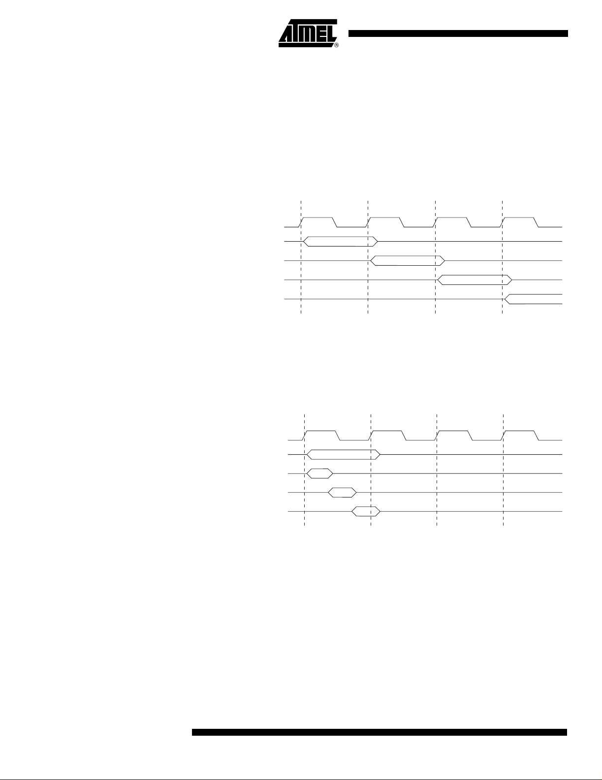
Instruction Execution Timing
This section describes the gener al access timing conc epts for i nstruct ion execut ion. The
AVR CPU is driven by the CPU clock clk
, directly generated from the selected clock
CPU
source for the chip. No internal clock division is used.
Figure 5 shows the parallel instructi on fetches and instruc tion exec utions enab led by the
Harvard architecture and the fast-access Register File concept. This is the basic pipelining concept t o obtain up t o 1 M IPS p er MH z with t he co rrespondin g u nique res ults for
functions per cost, functions per clocks, and functions per power-unit.
Figure 5. The Parallel Instruc ti on Fetches and Instruction Executions
T1 T2 T3 T4
clk
CPU
1st Instruction Fetch
1st Instruction Execute
2nd Instruction Fetch
2nd Instruction Execute
3rd Instruction Fetch
3rd Instruction Execute
4th Instruction Fetch
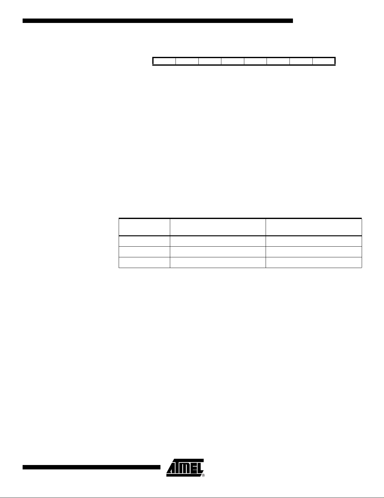
Figure 6 shows the internal timing concept for the Register File. In a single clock cycle
an ALU operation using two register operands is executed, and the result is stored back
to the destination regis ter.
Reset and Interrupt Handling
Figure 6. Single Cycle ALU Operation
T1 T2 T3 T4
clk
CPU
Total Execution Time
Register Operands Fetch
ALU Operation Execute
Result Write Back
The AVR provides several different interrupt sources. These interrupts and the separate
Reset Vector each have a separate Program Vector in the Program memory space. All
interrupts are assigned indi vidual en able bits w hich must b e wr itten logic one together
with the Global Interru pt Ena ble bit i n the Stat us Reg ister in orde r to enabl e the i nterr upt.
Depending on the Program Counter value, interrupts may be automatically disabled
when Boot Lock Bits BLB02 or BLB12 are programmed. This feature improves software
security. See the section “Memor y Programming” on page 219 for details.
The lowest addresse s in the Program memory spa ce are by default define d as the
Reset and Interrupt Vectors. The complete list of Vectors is shown in “Interrupts” on
page 44. The list also determines the priority levels of the different interrupts. The lower
the address the higher is the priority l evel. RESET ha s the highe st priority, and next is
INT0 – the External Interrupt Request 0. The Interrupt Vectors can be moved to the start
12
ATmega8(L)
2486M–AVR–12/03

ATmega8(L)
of the boot Flash section by settin g the Interrup t Vector Select (IVSEL) bit in t he General
Interrupt Control Register (GICR). Refer to “Interrupts” on page 44 for more information.
The Reset Vector can also be moved to the start of the boot Flash section by programming the BOOTRST Fuse, see “Boot Loader Support – Read-While-Write SelfProgramming” on page 206.
When an interrupt occurs, the Global In terrupt Enab le I-bit is cleared and al l interrupts
are disabled. The user softw are ca n wri te logi c on e to the I-bit t o en able n este d int errupts. All enabled interrupts can then i nterrupt the current interrupt routine. The I-bit is
automatically set when a Return from Interrupt instruction – RETI – is executed.
There are basicall y two types of inter rupts. The first type is triggered by an event that
sets the Interrupt Flag. For these interrupts, the Program Counter is vectored to the
actual Interrupt Vector in order to execute the interrupt handling routine, and hardware
clears the corresponding Interrupt Flag. Interrupt Flags can also be cleared by writing a
logic one to the flag bi t posi tion( s) to be c leared. If an i nterr upt condi tion oc cur s while the
corresponding interrupt enable bit is cleared, the Interrupt Fl ag will be set and remembered until the interrupt is enabled, or the flag is cleared by software. Similarly, if one or
more interrupt conditions occur while the global interrupt enable bit is cleared, the cor responding Interrupt Flag(s) will be set and remembered until the globa l interrupt enable
bit is set, and will then be executed by order of pri ority.
The second type of interrupts will trigger as long as the interrupt condition is present.
These interrupts do not necessarily have Interrupt Flags. If the i nterrupt condition disappears before the interrupt is enabled, the interrupt will not be triggered.
When the AVR exits from an interrupt, it will alway s return to the main program and execute one more instruction before any pending interrupt is served.
Note that the Status Register is not automatically stored when entering an interrupt routine, nor restored when returning from an interrupt routine. This must be handled by
software.
When using the CLI instruction to disable interrupts, the interrupts will be immediately
disabled. No interrupt wil l be executed after the CLI instruction, even if it occurs simultaneously with the CLI instruction. The following example shows how this can be used to
avoid interrupts during the timed EEPROM write sequence.
Assembly Code Example
in r16, SREG ; store SREG value
cli ; disable interrupts during timed sequence
sbi EECR, EEMWE ; start EEPROM write
sbi EECR, EEWE
out SREG, r16 ; restore SREG value (I-bit)
C Code Example
char cSREG;
cSREG = SREG; /* store SREG value */
/* disable interrupts during timed sequence */
_CLI();
EECR |= (1<<EEMWE); /* start EEPROM write */
EECR |= (1<<EEWE);
SREG = cSREG; /* restore SREG value (I-bit) */
2486M–AVR–12/03
13

When using the SEI instruction to enable interrupts, the instruction following SEI will be
executed before any pending inter rupt s, as shown in the following example.
Assembly Code Example
sei ; set global interrupt enable
sleep; enter sleep, waiting for interrupt
; note: will enter sleep before any pending
; interrupt(s)
C Code Example
_SEI(); /* set global interrupt enable */
_SLEEP(); /* enter sleep, waiting for interrupt */
/* note: will enter sleep before any pending interrupt(s) */
Interrupt Response Time The interrupt execution response for all the enabled AVR interrupts is four clock cycles
minimum. After four clock cycles, the Program Vector address for the actual interrupt
handling routine is exe cuted. D uring th is 4-cloc k cycle p eriod, th e P rogram Counter is
pushed onto the Stack. Th e Vector is n ormally a jum p to the interrupt routine, and this
jump takes three clock cycles. If an interrupt occurs during execution of a multi-cycle
instruction, this instruction is completed before the interrupt is served. If an interrupt
occurs when the MCU is in sleep mode, the interrupt execution response time is
increased by four clock cycles. This increase comes in additio n to the st art-up time from
the selected sleep mode.
A return from an interrupt handling routine takes four clock cycles. During these four
clock cycles, the Program C ounter (2 byt es) is popped back from the St ack, the St ack
Pointer is incremented by 2, and the I-bit in SREG is set.
14
ATmega8(L)
2486M–AVR–12/03

ATmega8(L)
AVR ATmega8 Memories
In-System Reprogrammable Flash Program Memory
This section de scribes the di fferent mem ories in the A Tmega8. The AVR archit ecture
has two main memory spaces, the Data memory and the Program Memory space. In
addition, the ATmega8 features an EEPROM Memory for data storage. All three memory spaces are linear and regular.
The ATmega8 contains 8K bytes On-c hip In-Sys tem Repro gramma ble Flash memory
for program storage. Since all AVR instructions are 16- or 32-bits wide, the Flash is
organized as 4K x 16 bits. F or sof tware se curity, the Fla sh Prog ram m emory spac e is
divided into two sections, Boot Program section and Application Program secti on.
The Flash me mory has an endurance of at least 10 ,000 write/erase cycles. The
ATmega8 Program Counter (PC) is 12 bits wide, thus addressing the 4K Program memory locations. The operation of Boot Program section and associated Boot Lock Bits for
software protection are described in detail in “Boot Loader Support – Read-While-Write
Self-Programming” on page 206. “Memory Programming” on page 219 contains a
detailed description on Flash Programming in SPI- or Parallel Programming mode.
Constant tables can be all ocated within the entire Program memory addr ess space (see
the LPM – Load Program memory instruction description) .
Timing diagrams for instruction fetch and execution are presented in “Instruction Execution Timing” on page 12.
Figure 7. Program Memory Map
Application Flash Section
Boot Flash Section
$000
$FFF
2486M–AVR–12/03
15

SRAM Data Memory Figure 8 shows how the ATmega8 SRAM Memory is organized.
The lower 1120 Data memory locations address the Register File, the I/O Memory, and
the internal data SRAM. The first 96 locations ad dress the R egister File and I /O Memory, and the next 1024 locations address the internal data SRAM.
The five different addressing modes for the Data memory cover: Direct, Indirect with
Displacement, Indirect , Indi rect with Pre- decr ement, and Indir ect wit h Post-i ncre ment. In
the Register File, registers R26 to R31 feature the indirect addressing pointer registers.
The direct addressing rea ches the entire data space.
The Indirect with Displacement mode reaches 63 address locations from the base
address given by the Y- or Z-register.
When using register indirect addressing modes with automatic pre-decrement and post-
increment, the address regis ters X, Y and Z are decremented or incremented.
The 32 general purpose working registers, 64 I/O Register s, and the 1024 bytes of inter-
nal data SRAM in the ATmega8 are all accessible through all these addressing modes.
The Register File is described in “General Purpose Register File” on page 10.
Figure 8. Data Memory Map
Register File
Data Address Space
R0
R1
R2
...
R29
R30
R31
I/O Registers
$00
$01
$02
...
$3D
$3E
$3F
$0000
$0001
$0002
...
$001D
$001E
$001F
$0020
$0021
$0022
...
$005D
$005E
$005F
Internal SRAM
$0060
$0061
...
$045E
$045F
16
ATmega8(L)
2486M–AVR–12/03

ATmega8(L)
Data Memory Access Times
This section describes the general access timing concepts for internal memory access.
The internal data SRAM access is performed in two clk
cycles as described in Figure
CPU
9.
Figure 9. On-chip Data SRAM Access Cycles
T1 T2 T3
clk
CPU
Address
Data
WR
Data
RD
Compute Address
Memory Vccess Instruction
Address Valid
Write
Read
Next Instruction
EEPROM Data Memory The ATmega8 contains 512 bytes of data EEPROM memory. It is organized as a sepa-
rate data sp ace, in w hich si ngle b ytes can be re ad and writte n. Th e E EPRO M has an
enduranc e of at lea st 100, 000 write /erase cycle s. The acc ess be tween th e EEPR OM
and the CPU is described bellow, specifying the EEPROM Address Registers, the
EEPROM Data Register, and the EEPROM Control Register.
“Memory Programming” on page 219 contains a detailed description on EEPROM Programming in SPI- or Parallel Programming mode.
EEPROM Read/Write Access The EEPROM Access Registers are accessible in the I/O space.
The write access time for the EEPROM is given in Table 1 on page 19. A self-timing
function, however, lets the user software detect when the next byte can be written. If the
user code contains instructions that w rite the EEPROM , some precautions m ust be
taken. In heavily filtered power supplies, V
is likely to rise or fall slowly on Power-
CC
up/down. This causes the device for some period of time to run at a voltage lower than
specified as minimum for the clock frequency used. See “Preventing EEPROM Corruption” on page 21. for details on how to avoid probl ems in these situations.
In order to prevent unintenti onal EEPROM writes, a specific wr ite pro cedure must be f ollowed. Refer to the description of the EEPROM Control Register for details on this.
When the EEPROM is read, the CPU i s halted for four clock cycles before the next
instruction is execut ed. Wh en the E EPRO M is w ritten, the CPU is h alted fo r two cl ock
cycles before the next instr u ction is executed.
2486M–AVR–12/03
17

The EEPROM Address Register – EEARH and EEARL
Bit 15 14 13 12 11 10 9 8
– – – – – – – EEAR8 EEARH
EEAR7 EEAR6 EEAR5 EEAR4 EEAR3 EEAR2 EEAR1 EEAR0 EEARL
7 6 5 4 3 2 1 0
Read/Write R R R R R R R R/W
R/W R/W R/W R/W R/W R/W R/W R/W
Initial Valu e 0 0 0 0 0 0 0 X
X X X X X X X X
• Bits 15..9 – Res: Reserved Bits
These bits are reserved bits in t he ATmega8 and will alway s read as zero.
• Bits 8..0 – EEAR8..0: EEPROM Address
The EEPROM Ad dress Registers – EEAR H and EEARL – speci fy the EEPROM
address in the 512 bytes EEPROM space. The EEPROM data bytes are addressed linearly between 0 and 511. The ini tial val ue o f EEAR is undefi ned. A proper value must be
written before the EEPROM may be accessed.
The EEPROM Data Register – EEDR
The EEPROM Control Register – EECR
Bit 7 6 5 4 3 2 1 0
MSB LSB EEDR
Read/Write R/W R/W R/W R/W R/W R/W R/W R/W
Initial Valu e 0 0 0 0 0 0 0 0
• Bits 7..0 – EEDR7..0: EEPROM Data
For the EEPROM write operation, the EEDR Register contains the data to be written to
the EEPROM in the address given by the EEAR Register. For the EEPROM read operation, the EEDR contains the data read out from the EEPROM at the address given by
EEAR.
Bit 7 6 5 4 3 2 1 0
– – – – EERIE EEMWE EEWE EERE EECR
Read/Write R R R R R/W R/W R/W R/W
Initial Valu e 0 0 0 0 0 0 X 0
• Bits 7..4 – Res: Reserved Bits
These bits are reserved bits in t he ATmega8 and will alway s read as zero.
• Bit 3 – EERIE: EEPROM Ready Interrupt Enable
Writing EERIE to one enables the EEPROM Ready Interrupt if the I bit in SREG is set.
Writing EERIE to zero disables the interrupt. The EEPROM Ready interrupt generates a
constant interrupt when EEWE is cleared.
• Bit 2 – EEMWE: EEPROM Master Write Enable
18
The EEMWE bit determines wh ether setting E EWE to one causes the EEP ROM to be
written. When EEMWE is set, setting EEWE within four clock cyc les will write data to the
EEPROM at the selected address If EEMWE is zero, setting EEWE will have no effect.
When EEMWE has been written to one by software, hardware cl ears the bit to zero after
four clock cycles. See the description of the EEWE bit for an EEPROM write procedure.
• Bit 1 – EEWE: EEPROM Write Enable
The EEPROM Write Enable Signal EEWE is the write strobe to the EEPROM. When
address and data are correctly set up, the EEWE bit must be written to one to write the
ATmega8(L)
2486M–AVR–12/03

ATmega8(L)
value into the EEPROM. The EEMWE bit must be written to one before a logical one is
written to EEWE, otherwise no EEPROM write takes place. The following procedure
should be followed when writing the EEPROM (the order of steps 3 and 4 is not
essential):
1. Wait until EEWE becomes zero.
2. Wait until SPMEN in SPMCR becomes zero.
3. Write new EEPROM address to EEAR (optional).
4. Write new EEPROM data to EEDR (optional).
5. Write a logical one to the EEMWE bit while writing a zero to EEWE in EECR.
6. Within four clock cycles afte r setting EEMWE, write a logical one to EEWE.
The EEPROM can not be progra mmed du ring a CPU write to the Flash me mory. The
software must check that the Flash programming is completed before initiating a new
EEPROM writ e. St ep 2 is o nly rel evant i f the s oftwa re c ontain s a b oot loader al lowing
the CPU to program the F lash. If the F lash is never being u pdated by the CPU, st ep 2
can be omitted. See “Boot Loa der Suppo rt – Read-While-Writ e Self-Programmin g” on
page 206 for details about boot programming.
Caution: An interrupt between step 5 and step 6 will make the write cycle fail, since the
EEPROM Master Write Enable will time-out. If an interrupt routine accessing the
EEPROM is interrupting another EEPROM access, the EEAR or EEDR Register will be
modified, causing th e inte rrupted E EPROM acce ss to fa il. It is recom mended to ha ve
the Global Interrupt Flag cleared during all the steps to avoid these problems.
When the write access time has elapsed, the EEWE bit is cleared by hardware. The
user software can poll this bit and wait for a zero before writing the next byte. When
EEWE has been set, the CPU is halted for two cycles before the n ext instruction is
executed.
• Bit 0 – EERE: EEPROM Read Enable
The EEPROM Read Enable Signal EERE is the read strobe to the EEPROM. When the
correct address is set up in the EEAR Register, the EERE bit must be written to a logic
one to trigger the EEPROM read. The EEPROM read access takes one instruction, and
the requested data is available immediately. When the EEPROM is read, the CPU is
halted for four cycles before the next instruction is executed.
The user should poll the EEWE bit be fore st artin g the read oper ation. If a wri te opera tion
is in progress, it is neither pos sible to read the EEPRO M, nor to change the EEAR
Register.
The calibrated Oscil lator is used to ti me the EEPROM accesses. Table 1 li sts the typical
programming time for EEPROM access from the CPU.
Table 1. EEPROM Programming Time
Number of Calibrated RC
Symbol
EEPROM Write (from CPU) 8448 8.5 ms
Note: 1. Uses 1 MHz clock, independent of CKSEL Fuse settings.
Oscillator Cycles
(1)
Typ Programming Time
2486M–AVR–12/03
19

The following code examples show one assembly and on e C function for writing to the
EEPROM. The examples assume that i nterrupts are controlled (for example by disabling interrupts glob ally) so that no interrupts will occur during execution of these
functions. The exam ples also assume t hat no Flash boo t loader is present in the software. If such code is present, the EEPROM write function must also wait for any
ongoing SPM command to finish.
Assembly Code Example
EEPROM_write:
; Wait for completion of previous write
sbic EECR,EEWE
rjmp EEPROM_write
; Set up address (r18:r17) in address register
out EEARH, r18
out EEARL, r17
; Write data (r16) to data register
out EEDR,r16
; Write logical one to EEMWE
sbi EECR,EEMWE
; Start eeprom write by setting EEWE
sbi EECR,EEWE
ret
C Code Example
void EEPROM_write(unsigned int uiAddress, unsigned char ucData)
{
/* Wait for completion of previous write */
while(EECR & (1<<EEWE))
;
/* Set up address and data registers */
EEAR = uiAddress;
EEDR = ucData;
/* Write logical one to EEMWE */
EECR |= (1<<EEMWE);
/* Start eeprom write by setting EEWE */
EECR |= (1<<EEWE);
}
20
ATmega8(L)
2486M–AVR–12/03

ATmega8(L)
The next code examples show assembly and C functions for reading the EEPROM. The
examples assume that interru pts are controlled so that no interrupts will occur during
execution of these functions.
Assembly Code Example
EEPROM_read:
; Wait for completion of previous write
sbic EECR,EEWE
rjmp EEPROM_read
; Set up address (r18:r17) in address register
out EEARH, r18
out EEARL, r17
; Start eeprom read by writing EERE
sbi EECR,EERE
; Read data from data register
in r16,EEDR
ret
C Code Example
unsigned char EEPROM_read(unsigned int uiAddress)
{
/* Wait for completion of previous write */
while(EECR & (1<<EEWE))
;
/* Set up address register */
EEAR = uiAddress;
/* Start eeprom read by writing EERE */
EECR |= (1<<EERE);
/* Return data from data register */
return EEDR;
}
EEPROM Write during Powerdown Sleep Mode
Preventing EEPROM Corruption
2486M–AVR–12/03
When entering Power-down sleep mode whi le an EEPROM write opera tion i s activ e, the
EEPROM write operation will continue, and will complete before the Write Access time
has passed. However, when the write operation is completed, the Oscillator conti nues
running, and as a consequence, the device does not enter Power-down entirely. It is
therefore recommended to verify that the EEPROM write operation is completed before
entering Power-down.
During periods of low V
the EEPROM data can be corrupted because the supply volt-
CC,
age is too low for the CPU and the EEPROM to operate properly. These issues are the
same as for board level systems using EEPROM, and the same design solutions should
be applied.
An EEPROM data corruption can be caused by two situations wh en the voltage is too
low. First, a regular write sequence to t he EEPROM requires a minimum volt age to
operate correctly. Second, the CPU itself can execute instructions incorrectly, if the supply voltage is too low.
EEPROM da ta corruption can easily be avoided by fol lowing this design
recommendation:
21

Keep the AVR RESET active (low) during periods of insufficient power supply voltage. This can be done by enabling the internal Brown-out Detector (BOD). If the
detection level of the intern al BOD does no t match the needed det ection l evel, an
external low V
operation is in progress, the write operation will be completed provided that the
power supply voltage is suffici ent.
Reset Protection circuit can be used. If a reset occurs while a write
CC
I/O Memory The I/O space definition of the ATmega8 is shown in “” on page 282.
All ATmega8 I/Os and peripherals are placed in the I/O space. The I/O locations are
accessed by the IN and OUT instructions, transferring data between the 32 general purpose working registers and the I/O space. I/O Registers within the address range 0x00 0x1F are directly bit-acces sible using the SBI and CB I instructions. In these re gisters,
the value of single bits can be checked by using the SBIS and SBIC instructions. Refer
to the instruction set sec ti on for more details. When using the I/O specific commands IN
and OUT, the I/O addresses 0x00 - 0x3F must be used. When addressing I/O Registers
as data space using LD and ST instructions, 0x20 must be added to t hese addresses.
For compatibility wit h future devices, rese rved bits should be written to zero if accessed.
Reserved I/O memory addresses should never be written.
Some of the Status Flags are cleared by writi ng a logical one to them. Note that the CBI
and SBI instructions will operate on all bits in the I/O Register, writing a one back into
any flag read as set, thus clearing the flag. The CBI and SBI instructions work with registers 0x00 to 0x1F only.
The I/O and Peripherals Control Registers are explained in later sections.
22
ATmega8(L)
2486M–AVR–12/03

System Clock and Clock Options
ATmega8(L)
Clock Systems and their Distribution
Figure 10 presen ts the princip al clo ck system s in the AV R and the ir distributi on. All of
the clocks need not be active at a given time. In order to redu ce power consump tion, the
clocks to modules not being used can be halted by using different sleep modes, as
described in “Power Management and Sleep Modes” on page 31. The clock systems
are detailed Figure 10.
Figure 10. Clock Distribution
Asynchronous
Timer/Counter
General I/O
Modules
clk
clk
ASY
ADC CPU Core RAM
clk
ADC
I/O
AVR Clock
Control Unit
Source Clock
Clock
Multiplexer
clk
CPU
clk
FLASH
Reset Logic
Watchdog Timer
Watchdog Clock
Watchdog
Oscillator
Flash and
EEPROM
CPU Clock – clk
I/O Clock – clk
I/O
Flash Clock – clk
2486M–AVR–12/03
CPU
FLASH
Timer/Counter
Oscillator
External RC
Oscillator
External Clock
Crystal
Oscillator
Low-Frequency
Crystal Oscillator
Calibrated RC
Oscillator
The CPU clock is routed to parts of the system concerned with operation of the AVR
core. Examples of such module s are the General Purpose Reg ister File, the Stat us Register and the Data memory holding the Stack Pointer. Halting the CPU clock inhibits the
core from performing general operations and calculations.
The I/O clock is used by the majority of the I/O modules, like Timer/Counters, SPI, and
USART. The I/O clock is also used by the External Interrupt module, but note that some
external inter rupts are d etected by as ynchrono us logic, al lowing suc h interrup ts to be
detected even if the I/O cloc k is halted. Also note that address recogniti on in the TWI
module is carried out async hronousl y when clk
is halted, enabling TWI address recep -
I/O
tion in all sleep modes.
The Flash clock controls operation of the Flash interface. The Flash clock is usually
active simultaneously with th e CPU clock.
23

Asynchronous Timer Clock –
clk
ASY
The Asynchronous Timer cl ock allo ws the A synchronous Tim er/Counter t o be c locked
directly from an external 32 kHz clock crystal. The dedicated clock domain allows using
this Timer/Counter as a real-time counte r even when the device is i n sleep mod e. The
Asynchronous Timer/Counter uses the same XTAL pins as the CPU m ain clock but
requires a CPU main clock frequency of more than four times the Oscillator frequency.
Thus, asynchronous operation is only available while the chip is clocked on the Internal
Oscillator.
ADC Clock – clk
ADC
The ADC is provid ed with a ded icated clock do main. Thi s allows ha lting the C PU and
I/O clocks in order to reduce noise generated by digital circuitry. This gives more accurate ADC conversion results.
Clock Sources The device has the following clock source options, selectable by Flash Fuse Bits as
shown below. The clock from the selected source is input to the A VR cl ock gene rator,
and routed to the appropriate module s.
Table 2. Device Clocking Options Select
Device Clocking Option CKSEL3..0
External Crystal/Ceramic Resonator 1111 - 1010
External Low-frequency Crystal 1001
External RC Oscillator 1000 - 0101
Calibrated Internal RC Oscillator 0100 - 0001
External Clock 0000
Note: 1. For all fuses “1” means unprogrammed while “0” means programmed.
The various choices for each clocki ng optio n is given i n the followi ng secti ons. When the
CPU wakes u p from P ower-dow n or Po wer-sa ve, the sel ected cl ock so urce is used to
time the start-up, ens uring st able Osci llat or op erati on before i nstruc tion exe cuti on star ts.
When the CPU starts from reset, t here is as an add itional delay allowin g th e powe r to
reach a stable level before com mencing norm al operation. The Wat chdog Oscil lator is
used for timing this real-tim e part of the start-u p time. The numb er of WDT Oscilla tor
cycles used for each time-o ut is shown in Table 3. The frequ ency of the Wa tchdog
Oscillator is voltage dependent as shown in “ATmega8 Typical Characteristics”. The
device is shipped with CKSEL = “0001” and SUT = “10” (1 MHz I nternal RC Oscillator,
slowly rising power) .
(1)
24
Table 3. Number of Watchdog Oscillator Cycles
Typical Tim e- ou t (VCC = 5.0V) Typical Ti me-out (VCC = 3.0V) Number of Cycles
4.1 ms 4.3 ms 4K (4,096)
65 ms 69 ms 64K (65,536)
ATmega8(L)
2486M–AVR–12/03

ATmega8(L)
Crystal Oscillator XTAL1 and XTAL2 are input and output, respectively, of an inverting amplifier which can
be configured for use as an On-chip Osc illator, as shown i n F igure 11. Either a quartz
crystal or a ceramic resonator may be used. The CKOPT Fuse selects between two different Oscillator amplifier modes. When CKOPT is programmed, the Oscillator output
will oscillate a full rail-to-rail swing on the output. This mode is suitable when operating
in a very noisy environ ment or when the outpu t from XTAL2 drive s a second clock
buffer. This mode has a wide frequency range. When CKOPT is unprogrammed, the
Oscillator has a smaller output swing. T his reduces power consumption conside rably.
This mode has a limited frequency range and it cannot be used to drive other clock
buffers.
For resonators, the maximum frequency is 8 MHz with CK OPT unpro grammed and
16 MHz with CKOPT programmed. C1 and C2 should always be equal for both crystals
and resonators. The optimal value of the capacitors depends on the cryst al or resonator
in use, the amount of stray capacitance, an d the electromagn etic noise of the environment. Some initial gu ideline s for choosing capa citors for use with c rystals are g iven in
Table 4. For ceramic resonators, the capac itor values given by the manufacturer should
be used.
Figure 11. Crystal Oscillator Connections
C2
C1
XTAL2
XTAL1
GND
The Oscillator can operate in three different modes, each optimized for a specific frequency range. The operating mode is selected by the fuses CKSEL3..1 as shown in
Table 4.
Table 4. Crystal Oscillator Operating Modes
Frequency
CKOPT CKSEL3..1
1 101
1 110 0.9 - 3.0 12 - 22
1 111 3.0 - 8.0 12 - 22
0 101, 110, 111 1.0 ≤ 12 - 22
Note: 1. This option should not be used with crystals, only with ceramic resonators.
(1)
Range(MHz)
0.4 - 0.9 –
Recommended Range for Capacitors
C1 and C2 for Use with Crystals (pF)
2486M–AVR–12/03
The CKSEL0 Fuse together with the SUT1..0 Fuses select the start-up times as shown
in Table 5.
25

Table 5. Start-up Times for the Crystal Oscillator Clock Selection
Start-up Time
from Power-down
CKSEL0 SUT1..0
0 00 258 CK
0 01 258 CK
0 10 1K CK
0 11 1K CK
1 00 1K CK
1 01 16K CK –
1 10 16K CK 4.1 ms
1 11 16K CK 65 ms
Notes: 1. These options should only be used when not operating close to the maximum fre-
quency of the device, and only if frequency stability at start-up is not important for the
application. These options are not suitable for crystals.
2. These options are intended for use with ceramic resonators and will ensure frequency stability at start-up. They can also be used with crystals when not operating
close to the maximum frequency of the device, and if frequency stability at start-up is
not important for the application.
and Power-save
(1)
(1)
(2)
(2)
(2)
Addition al Delay
from Reset
(VCC = 5.0V) Recommended Us age
4.1 ms
65 ms
–
4.1 ms
65 ms
Ceramic resonator, fast
rising power
Ceramic resonator, slowly
rising power
Ceramic resonator , BOD
enabled
Ceramic resonator, fast
rising power
Ceramic resonator, slowly
rising power
Crystal Oscillator, BOD
enabled
Crystal Oscillator, fast
rising power
Crystal Oscillator, slowly
rising power
Low-frequency Crystal Oscillator
To use a 32.7 68 kHz w atch crystal as the clo ck source for the device , the Low-f requency Crystal Oscillator must be selected by setting the CKSEL Fuses to “1001”. The
crystal should be connected as shown in Figure 11. By programming the CKOPT Fuse,
the user can enable internal capacitors on XTAL1 and XTAL2, thereby removing the
need for external capacitors. The internal capacitors have a nominal value of 36 pF.
When this Oscilla tor is sele cted, sta rt-up times are determ ined by the SUT Fuse s as
shown in Table 6.
Table 6. Start-up Times for the Low-frequency Crystal Oscillator Clock Selection
Start-up Time from
Power-down and
SUT1..0
00 1K CK
01 1K CK
10 32K CK 65 ms Stable frequency at start-up
11 Reserved
Note: 1. These options should o nly be u sed if frequency stability a t sta rt-up is not imp ortant fo r
Power-save
(1)
(1)
the application.
Additional Delay
from Reset
(VCC = 5.0V) Recommended Usage
4.1 ms Fast rising power or BOD enabled
65 ms Slowly rising power
26
ATmega8(L)
2486M–AVR–12/03

ATmega8(L)
External RC Oscillator For timing insensitive applications, the external RC configuration shown in Figure 12
can be used. The frequency is roughly estimated by the equation f = 1/(3RC). C should
be at least 22 pF. By programming the CKOPT Fuse, the user can enable an inter nal 36
pF capacitor bet ween XTAL1 a nd GND, thereby rem oving the need for an external
capacitor. For more information on Oscillator operation and details on how to choose R
and C, refer to the External RC Oscillator application note.
Figure 12. External RC Configuration
V
CC
R
NC
XTAL2
XTAL1
C
GND
The Oscillator can operate in four different modes, each optimized for a specific frequency range. The operating mode is selected by the fuses CKSEL3..0 as shown in
Table 7.
Table 7. External RC Oscillator Operating Modes
CKSEL3..0 Frequency Range (MHz)
0101 ≤ 0.9
0110 0.9 - 3.0
0111 3.0 - 8.0
1000 8.0 - 12.0
When this Oscilla tor is sele cted, sta rt-up times are determ ined by the SUT Fuse s as
shown in Table 8.
2486M–AVR–12/03
Table 8. Start-up Times for the External RC Oscillator Clock Selection
Start-up Time from
Power-down and
SUT1..0
00 18 CK – BOD enabled
01 18 CK 4.1 ms Fast rising power
10 18 CK 65 ms Slowly rising power
11 6 CK
Note: 1. This option should not be used when operating close to the maximum frequency of
Power-save
(1)
the device.
Additional Delay
from Reset
= 5.0V) Recommended Usage
(V
CC
4.1 ms Fast rising power or BOD enabled
27

Calibrated Internal RC Oscillator
The calibrated internal RC Oscillator provides a fixed 1.0, 2.0, 4.0, or 8.0 MHz clock. All
frequencies are nominal values at 5V and 25°C. This clock may be selected as the system clock by programming the CKSEL Fuses as shown in Table 9. If selected, it will
operate with no external components. The CKOPT Fuse should always be unprogrammed when using this clo ck optio n. Durin g reset, hardwa re loads t he cali brati on byte
into the OSCCAL Register and ther eby automat ically cal ibra tes the RC Osci llat or. At 5V,
25°C and 1.0 MHz O scillator frequen cy selected, thi s calibration gi ves a freq uency
within ± 3% of the nominal frequency. Using run-time calibration methods as described
in application notes availab le at www.atmel.com/avr it is possible to achieve ± 1% accuracy at any given V
and Temperature. When this Oscillator is used as the chip clock,
CC
the Watchdog Oscillator will still be used for the Watchdog T imer and for the Reset
Time-out. For more information on the pre-programmed ca libration value, see the section “Calibration Byte” on page 221.
Table 9. Internal Calibrated RC Oscillator Operati ng Mo des
CKSEL3..0 Nominal Frequency (MHz)
(1)
0001
0010 2.0
0011 4.0
0100 8.0
Note: 1. The device is shipped with this option selected.
1.0
When this Oscilla tor is sele cted, sta rt-up times are determ ined by the SUT Fuse s as
shown in Table 10. PB6 (XTAL1/TOS C1) and PB7(XT AL2/TOSC2) can be used a s
either general I/O pins or Timer Oscillator pins ..
Table 10. Start-up Times for the Internal Calibrated RC Oscillator Clock Selection
Start-up Time fro m
Power-down and
SUT1..0
00 6 CK – BOD enabled
01 6 CK 4.1 ms Fast rising power
(1)
10
11 Reserved
Note: 1. The device is shipped with this option selected.
Power-save
6 CK 65 ms Slowly rising power
Additional Del ay
from Reset
(V
= 5.0V) Recommended Usage
CC
28
ATmega8(L)
2486M–AVR–12/03
ATmega8(L)
Oscillator Calibrat ion Register – OSCCAL
Bit 7 6 5 4 3 2 1 0
CAL7 CAL6 CAL5 CAL4 CAL3 CAL2 CAL1 CAL0 OSCCAL
Read/Write R/W R/W R/W R/W R/W R/W R/W R/W
Initial Valu e Device Specific Calibration Value
• Bits 7..0 – CAL7..0: Oscillator Calibration Value
Writing the calibration byte to this address will trim the Internal Oscillator to remove process variations from the Oscillator frequency. During Reset, the 1 MHz calibration value
which is located in the signa ture row H igh byte (add ress 0x00) is automatically loaded
into the OSCCAL Register. If th e inter nal RC is us ed at o ther frequen cie s, the cali bra tion
values must be loaded manually. This can be done by first reading the signature row by
a programmer, and then store the calibration values in the Flash or EEPROM. Then the
value can be read by software an d lo aded into the OSCCAL Regi ste r. When OSCCAL is
zero, the lowest available frequency is chosen. Writing non-zero va lues to this register
will increase the frequency of the Internal O scillator. Wr iting 0xFF to the register gi ves
the highest available frequency. The calibrated Oscillator is used to time EEPROM and
Flash access. If EEPROM or Flash is written, do not calibrate to more than 10% above
the nominal fre quency. Otherw ise, the EEP ROM or F lash write m ay fai l. No te that the
Oscillator is intend ed fo r cali bration t o 1. 0, 2.0, 4.0, or 8. 0 MHz. Tuning to other values is
not guaranteed, as indicated i n Table 11.
Table 11. Internal RC Oscillator Frequency Range
OSCCAL Value
Min Frequency in Percentage of
Nominal Frequency (%)
Max Frequency in P er cent ag e o f
Nominal Freque ncy (%)
0x00 50 100
0x7F 75 150
0xFF 100 200
2486M–AVR–12/03
29

External Clock To drive the device from an external clock source, XTAL1 should be driven as shown in
Figure 13. To run the de vice on an exte rnal clock, the CK SEL Fuses must be programmed to “0000”. By programming the CKOPT Fuse, the user can enable an internal
36 pF capacitor between XTAL1 and GND.
Figure 13. External Clock Drive Configuration
EXTERNAL
CLOCK
SIGNAL
When this clock source is selected, start-up times are determined by the SUT Fuses as
shown in Table 12.
Table 12. Start-up Times for the External Clock Selection
Start-up Time fro m
Power-down and
SUT1..0
00 6 CK – BOD enabled
01 6 CK 4.1 ms Fast rising power
10 6 CK 65 ms Slowly rising power
11 Reserved
Power-save
Additional Del ay
from Reset
(VCC = 5.0V) Recommended Usage
When applying an external clock, it is required to avoid sudden changes in the applied
clock frequency to ensure stable operation of the MCU. A vari ation in frequency of more
than 2% from one clock cycle to the next can lead to unpredictable behavior. It is
required to ensu re that th e MCU is kept in Reset during such changes in the clock
frequency.
Timer/Counter Oscillator For AVR microcontrollers with Timer/Counter Oscillator pins (TOSC1 and TOSC2), the
crystal is connected directly betwe en the p ins. B y pro gramming the CK OPT Fuse, the
user can enable internal capacito rs on XTAL1 and XTAL 2, thereby rem oving the need
for external capacit ors. The Osci llat or is opt imized f or use wit h a 32.768 kHz watch crystal. Applying an external clock source to TOSC1 is not recommended.
30
ATmega8(L)
2486M–AVR–12/03

ATmega8(L)
Power Management and Sleep Mo des
MCU Control Register – MCUCR
Sleep modes enable the application to shut down unused modules in the MCU, thereby
saving power. The AVR provides various sleep modes allowing the user to tailor the
power consumption to the application’s requirements.
To enter any of the five sleep modes, the SE bit in MCUCR must be written to logic one
and a SLEEP instruction must be execut ed. The SM2, SM1, and SM0 bits in the
MCUCR Registe r select which sle ep mode (Idle, ADC No ise Reducti on, Power-do wn,
Power-save, or Standby) will be activated by the SLEEP instruction. See Table 13 for a
summary. If an ena bled int errup t occurs while the MCU is in a sl eep mo de, the M CU
wakes up. The MCU is then halted for four cycles in addition to the start-up time, it executes the interrupt routi ne, and res umes executi on from the i nstructi on foll owing SLEEP.
The contents of the R egister F ile and SRA M are u naltered w hen the device wa kes up
from sleep. If a reset occurs during sleep mode, the MCU wakes up and executes from
the Reset Vector.
Note that the Extended Standby m ode present in many o ther AVR MC Us has been
removed in the ATmega8, as the TOSC and XTAL inputs share the same physical pins.
Figure 10 on page 23 presents t he differen t clock system s in the ATme ga8, and th eir
distribution. The figure is helpful in selecting an appropriate sleep mode.
The MCU Control Register contains control bits for power management.
Bit 7 6 5 4 3 2 1 0
SE SM2 SM 1 SM0 ISC11 ISC10 ISC01 ISC00 MCUCR
Read/Write R/W R/W R/W R/W R/W R/W R/W R/W
Initial Valu e 0 0 0 0 0 0 0 0
• Bit 7 – SE: Sleep Enable
The SE bit must be written to lo gic one t o make the MCU enter the sle ep mode when the
SLEEP instruction is executed. To avoi d the MCU entering the sleep mode unl ess it is
the programmer’s purpose, it is recomme nded to set the Sl eep Enable (SE) bi t just
before the execution of the SLEEP instruction.
• Bits 6..4 – SM2..0: Sleep Mode Select Bits 2, 1, and 0
These bits select between the five available sleep modes as shown in Table 13.
Table 13. Sleep Mode Select
SM2 SM1 SM0 Sleep Mode
0 0 0 Idle
0 0 1 ADC Noise Reduction
0 1 0 Power-down
0 1 1 Power-save
1 0 0 Reserved
1 0 1 Reserved
1 1 0 Standby
Note: 1. Standby mode is only available with external crystals or resonators.
(1)
2486M–AVR–12/03
31

Idle Mode W hen the SM 2..0 bit s are written to 000, the SLEE P instructi on makes the MCU enter
Idle mode, stopping the CPU but allowing SPI, USART, Analog Comparat or, ADC, Twowire Serial Interface, Timer/Counters, Wa tchdog, and the interrupt system to continue
operating. This sleep mode basically halts clk
CPU
and clk
clocks to run.
Idle mode enables the MCU to wake up from external triggered interrupts as well as
internal ones like the Timer Overflow and USART Transmit Complete interrupts. If
wake-up from the Analog Comparator interrupt is not required, the Analog Comparator
can be powered down by setting the ACD bit in the Analog Comparator Control and Status Register – ACSR . This will redu ce power con sumptio n in Idle mode . If the ADC is
enabled, a conversion start s automat ically when this mode is entered.
, while allowing the other
FLASH
ADC Noise Reduction Mode
When the SM2..0 bit s are written to 001, the SLEE P instructi on makes the MCU enter
ADC Noise Red uction mode , stopping the CPU but allowing the ADC , the external
interrupts, the Two-wire Serial Interface address watch, Timer/Counter2 and the
Watchdog to continue operating (if e nabled). This sleep mode basically halts clk
clk
CPU
, and clk
, while allowing the other clocks to run.
FLASH
I/O
This improves the noise environment for the ADC, enabling higher resolution measurements. If the ADC is enabled, a conversion starts automatically when this mode is
entered. Apart form the ADC Conversion Complete interrupt, only an External Reset, a
Watchdog Reset, a Brown-out Reset, a Tw o-wire Serial Interface address match int errupt, a Timer/Counter2 interrupt, an SPM/EEPROM ready interrupt, or an external level
interrupt on INT0 or INT1, can wake up the MCU from ADC Noise Reduction mode.
Power-down Mode When the SM2..0 bits are wri tten to 01 0, the SLEE P instructi on makes the MCU enter
Power-down mode. I n this mode , the E xternal Osci llator is sto pped, whil e the externa l
interrupts, the Two-wire Serial Interface address watch, and the Watchdog continue
operating (if enabled ). Only an Ext ernal Res et, a Watchdo g Reset, a Brown- out Reset , a
Two-wire Serial Interface address match interrupt, or an external level interrupt on INT0
or INT1, can wake up the M CU. This sle ep mode basi cally halts all generated clo cks,
allowing operation of asynchronous modules only.
Note that if a level triggered interrupt is used for wake-up f rom Power-down mode, the
changed level must be held for some time to wake up the MCU. Refe r to “External Interrupts” on page 64 for details.
When waking up from Power-down mode, there is a delay from the wake -up con dition
occurs until the wake-up becomes effective. This allows the clock to r estart and become
stable after having been stopp ed. The wake-u p p eriod is defined b y th e same CKS EL
Fuses that define the Reset Time-out period, as described in “Clock Sources” on page
24.
,
Power-save Mode When the SM2..0 bi ts are wri tten to 01 1, the SLEE P instruct ion makes the MCU enter
Power-save mode. This mode is identical to Power-down, with one exception:
If Timer/Counter2 is clocked asynchronously, i.e. the AS2 bit in ASSR is set,
Timer/Counter2 will run during sleep. The device can wake up from either Timer
Overflow or Output Compare event from Timer/Counter2 if the corresponding
Timer/Counter2 i nterrupt enable bits are set in TIMSK, and the g lobal int errupt
enable bit in SREG is set.
If the asynchronous timer is NOT clocked asynchronously, Power-down mode is recommended instead of Power-save mode because the contents of the registers in the
32
ATmega8(L)
2486M–AVR–12/03

ATmega8(L)
asynchronous timer should be considered undefined after wake-up in Power- save mode
if AS2 is 0.
This sleep mode basicall y halts all clocks except clk
, allowing operation only of asyn-
ASY
chronous modules, including Timer/Counter 2 if clocked asynchronously.
Standby Mode When the SM2..0 bits are 110 and an external crystal/resonator clock opt ion is selected,
the SLEEP instruction ma kes the MCU enter Stan dby mode. This mode i s identical to
Power-down with the exception that the Oscillator is kept running. From Standby mode,
the device wakes up in 6 clock cycles.
Table 14. Active Clock Domains and Wake-up Sources in the Different Sleep Modes
Active Clock Domains Oscillators Wake-up Sources
Sleep
Mode
clk
CPU
clk
FLASH
clkIOclk
ADC
clk
Main Clock
Source Enabled
ASY
Timer Osc.
Enabled
Idle X X X X X
ADC Noise
Reduction
X X X X
Power
Down
Power
Save
Standby
(1)
(2)
X
X X
Notes: 1. External Crystal or resonator selected as clock source.
2. If AS2 bit in ASSR is set.
3. Only level interrupt INT1 and INT0.
TWI
INT1
Address
INT0
Match
(2)
(2)
(2)
X
X X X X X X
(3)
X
(3)
X
(3)
X
(3)
Timer
X X X X
X
X X
X
2
(2)
SPM/
EEPROM
Ready
ADC
Other
I/O
Minimizing Power Consumption
There are several issues to consider when trying to minimize the power consumption in
an AVR controlled system. In general, sleep modes should be used as much as possible, and the slee p mode shoul d be se lected s o that as few a s p ossible of the devi ce’s
functions are op erating. A ll function s no t needed shoul d be d isabled. In part icular, the
following modules may need special consideration when trying to achieve the lowest
possible power consumption.
Analog-to-Digital Converter (ADC)
If enabled, the ADC will be enabled in all sleep modes. To save power, the ADC should
be disabled before entering any sleep mode. When the ADC is turned off and on again,
the next conve rsion will be a n extended conversion. Refer to “Analog-to-Digital Converter” on page 193 for details on ADC operation.
Analog Comparator When entering Idle mode, the Analog Comparator should be disabled if not used. When
entering ADC Noise Reduction mode, the Analog Compara tor should be disa bled. In the
other slee p modes , the Anal og Com parato r is automa tical ly disab led. Ho wever, if the
Analog Comparator is set up to use the Internal Voltage Reference as input, the Analog
Comparator should be disabled in all sleep modes. Otherwise, the Internal Voltage Reference will be enabled, independent of sleep mode. Refer to “Analog Compara tor” on
page 190 for details on how to configure the Analog Comparator.
2486M–AVR–12/03
33

Brown-out Detector If the Brown-out Detector is not needed in the application, this module should be turned
off. If the Brown-out Detector is enable d by the BODEN Fuse, it will be ena bled in all
sleep modes, and hence, always consum e power. In the de eper sleep mod es, this will
contribute significantly to the total current consumption. Refer to “Brown-out Detection”
on page 38 for details on how to configure the Brown-out Detector.
Internal Voltage Reference The Internal Voltage Ref erence will be enabled when nee ded by the Brown-out Detec-
tor, the Analog Comparator or t he ADC. I f these modu les are disabl ed as described i n
the sections above, the internal voltage reference will be disabled and it will not be consuming power. When turned on again, the user must allow the reference to start up
before the outpu t is us ed. If the reference is kep t on in sleep m ode, the out put can be
used immediately. Refe r to “In ternal Vol tage R eference” on page 4 0 for de tails on the
start-up time.
Watchdog Timer If the Watchdog Timer is not needed in the application, this module should be turned off.
If the Watchdog Timer is enab led, it will be ena bled in all sleep modes, and hence,
always consume power. In the deeper sleep mo des, this will contribute significant ly to
the total current consumption. Refer to “Watchdog Timer” on page 41 for details on how
to configure the Watchdog Timer.
Port Pins When entering a sleep mode, all port pins should be configured to use minimum power.
The most im portant t hing is th en to ensur e that no pins drive resistiv e loads . In sleep
modes where the both the I/O clock (clk
) and the ADC clock (clk
I/O
) are stopped, the
ADC
input buffers of the device will be disabled. This ensures that no power is consumed by
the input logic when not needed. In some cases, the input logic is needed for detecting
wake-up conditions, and it will then be enabled. Refer to the section “D igital Input
Enable and Sleep Modes” on page 53 for details on which pins are enabled. If the input
buffer is enabled and the input signal is left floating or have an analog signal level close
/2, the input buffer will use exce ssive power.
to V
CC
34
ATmega8(L)
2486M–AVR–12/03

ATmega8(L)
System Control and Reset
Resetting the AVR During Reset, all I/O Registers are set to their initial values, and the program starts exe-
cution from the Reset Vector. If the program never enables an interrupt source, the
Interrupt Vectors are not used, and regular program code can be placed at these locations. This is also the case if the Reset Vector is in the Application section while the
Interrupt Vectors are in the boot section or vice versa. The circuit diagram in Figure 14
shows the Reset Logic. Table 15 defines the electrical parameters of the reset circuitry.
The I/O ports of the AVR are immediately reset to their initial state when a reset source
goes active. This does not require any clock source to be running.
After all reset sources have gone inactive, a delay counter is invoked, stretching the
internal reset. This allows the power to reach a stable level before normal operation
starts. The time-out period of the delay counter is defined by the user through the
CKSEL Fuses. The different selections for the delay period are presented in “Clock
Sources” on page 24.
Reset Sources The ATmega8 has four sources of Reset:
• Power-on Reset. The MCU is reset when the supply voltage is below the Power- on
Reset threshold (V
• External Reset. The MCU is reset when a low level is present on the RESET pin for
longer than the minimum pulse length.
• Watchdog Reset. The MCU is reset when the Watchdog Timer period expires and
the Watchdog is enabled.
• Brown-out Reset. The MCU is reset when the supply voltage VCC is below the
Brown-out Reset threshold (V
POT
).
) and the Brown-out Detector is enabled.
BOT
2486M–AVR–12/03
35

Figure 14. Reset Logic
DATA BUS
MCU Control and Status
Register (MCUCSR)
BORF
PORF
WDRF
EXTRF
BODEN
BODLEVEL
Pull-up Resistor
SPIKE
FILTER
Brown-Out
Reset Circuit
Watchdog
Oscillator
Clock
Generator
CKSEL[3:0]
SUT[1:0]
CK
Delay Counters
TIMEOUT
Table 15. Reset Characteristics
Symbol Parameter Condition Min Typ Max Units
V
POT
Power-on Reset Threshold
Voltage (rising)
(1)
Power-on Reset Threshold
Voltage (falling)
1.4 2.3 V
1.3 2.3 V
36
ATmega8(L)
V
V
V
RST
t
RST
BOT
t
BOD
HYST
RESET Pin Threshold Voltage 0.1 0.9 V
Minimum pulse width on
RESET Pin
Brown-out Reset Threshold
Voltage
(2)
Minimum low voltage period for
Brown-out Detection
BODLEVEL = 1 2.4 2.6 2.9
BODLEVEL = 0 3.7 4.0 4.5
BODLEVEL = 1 2 µs
BODLEVEL = 0 2 µs
1.5 µs
Brown-out Detector hysteresis 130 mV
Notes: 1. The Power-on Reset will not work unless the supply voltage has been below V
(falling).
2. V
may be below nominal minimum operating voltage for some devices. For
BOT
devices where this is the case, the device is tested down to V
CC
= V
durin g the
BOT
production test. This guarantees that a Brown-out Reset will occur before V
CC
drops
to a voltage where correct operation of the microcontroller is no longer guaranteed.
The test is performed using BODLEVEL = 1 for ATmega8L and BODLEVEL = 0 for
ATmega8. BODLEVEL = 1 is not applicable for ATmega8.
2486M–AVR–12/03
CC
V
POT

ATmega8(L)
Power-on Reset A Power-on Reset (POR) pulse is generated by an On-chip detection circuit. The detec-
tion level i s defined in Table 15. Th e POR is a ctivated w heneve r V
detection level. The POR circuit can be used to trigger the Start-up Reset, as well as to
detect a failure in supply volt age.
A Power-on Reset (POR) circuit ensures that the device is reset from Power-on. Reaching the Power-on Reset threshold voltage invokes the delay counter, which determines
how long the device is kept in RESET after V
again, without any delay, when V
decreases below the detection level.
CC
rise. The RESET signal is activated
CC
is below the
CC
Figure 15. MCU Start-up, RESET Tied to V
V
V
CC
RESET
TIME-OUT
INTERNAL
RESET
POT
V
RST
t
TOUT
CC
Figure 16. MCU Start-up, RESET Extended Externally
V
V
CC
RESET
TIME-OUT
POT
V
RST
t
TOUT
2486M–AVR–12/03
INTERNAL
RESET
37

External Reset An External Reset is generated by a low level on the RESET pin. Reset pul ses longer
than the minimum pulse width (see T able 15) will generate a rese t, even if the clock is
not running. Shorter pulses are not guarante ed to generate a reset. When the applied
signal reaches the Reset Threshold Voltage – V
counter starts the MCU after the time-ou t peri od t
on its positive edge, th e delay
RST
has expired.
TOUT
Figure 17. External Reset During Operation
CC
Brown-out Detection ATmega8 has an On-chip Brown-out Detection (BOD) circuit for monitoring the V
level during operation by comparing it to a fixed trigge r level. The trigger level for the
BOD can be selected by the fuse BODLEVEL to be 2.7V (BODLEVEL unprogrammed),
or 4.0V (BODLE VEL program med). The tr igger leve l has a hyst eresis to ensu re s pike
free Brown-out Detection. The hysteresis on the detection level should be interpreted as
V
BOT+
= V
BOT
+ V
HYST
/2 and V
BOT-
= V
BOT
- V
HYST
/2.
The BOD circuit can be enabled/disabled by the fuse BODEN . When the BOD is
enabled (BODE N programmed), and V
(V
in Figure 18), the Brown-out Reset is immediately activated. When VCC increases
BOT-
above the trigger level (V
time-out period t
has expired.
TOUT
in Figure 18), the delay counter starts the MCU after the
BOT+
decreases to a valu e below the trigger level
CC
The BOD circuit will only detect a drop in VCC if the voltage stays below the trigger level
for longer than t
given in Table 15.
BOD
Figure 18. Brown-out Reset During Operation
V
CC
RESET
TIME-OUT
V
BOT-
V
BOT+
t
TOUT
CC
38
INTERNAL
RESET
ATmega8(L)
2486M–AVR–12/03

ATmega8(L)
Watchdog Reset When the Watchdog times out, it will generate a short reset pulse of 1 CK cycle dura-
tion. On the falling edge of this pulse, the delay timer starts counting the time-out period
. Refer to page 41 for details on operation of the Watchdog Timer.
t
TOUT
Figure 19. Watchdog Reset During Operation
CC
CK
MCU Control and Status Register – MCUCSR
The MCU Control and Status Register provides information on which reset source
caused an MCU Reset.
Bit 7 6 5 4 3 2 1 0
– – – – WDRF BORF EXTRF PORF MCUCSR
Read/Write R R R R R/W R/W R/W R/W
Initial Valu e 0 0 0 0 See Bit Description
• Bit 7..4 – Res: Reserved Bits
These bits are reserved bits in the ATmega8 and always read as zero.
• Bit 3 – WDRF: Watchdog Reset Flag
This bit is set if a Watchdog Reset occurs. The bi t is reset by a Pow er-on Reset, or by
writing a logic zero to the flag.
• Bit 2 – BORF: Brown-out Reset Flag
This bit is set if a Brown-out Reset occurs. The bit is reset by a Powe r-on Reset, or by
writing a logic zero to the flag.
• Bit 1 – EXTRF: External Reset Flag
This bit is set i f an E xternal R eset occ urs. T he bit is reset by a Power-on Reset, or by
writing a logic zero to the flag.
• Bit 0 – PORF: Power-on Reset Flag
This bit is set if a Power-on Reset occurs. The bit is reset only by writing a logic zero to
the flag.
2486M–AVR–12/03
To make use of the Reset Flags to identify a reset condition, the user should re ad and
then reset the MCUCSR as early as possible in the program. If the register is cleared
before another reset occurs, the source of the reset can be found by examining the
Reset Flags.
39

Internal Voltage Reference
ATmega8 features an internal bandgap reference. This reference is used for Brown-out
Detection, and it can be used as an input to the Analog Comparator or the ADC. The
2.56V reference to the ADC is generated from the int ernal bandgap reference.
Voltage Reference Enable Signals and Start-up Time
The voltage reference has a start-up time that may influence the way it should be used.
The start-up time is given i n Table 16. To s ave power, the r eference is n ot always tur ned
on. The reference is on during the follo wing situations:
1. When the BOD is enabled (by programming the BODEN Fuse).
2. When the bandgap reference is connected to the Analog Compara tor (by setting
the ACBG bit in ACSR).
3. When the ADC is enabled.
Thus, when the BOD is not enabled, after setti ng the ACBG bit or enabling the ADC, the
user must always allow the refer ence t o start up befo re the out put from the Anal og Comparator or ADC is used. To reduce powe r consumption in Pow er-down mode, the user
can avoid the three co nditions above to en sure that the reference is turne d off before
entering Power-down mode.
Table 16. Internal Voltage Reference Characteristics
Symbol Parameter Min Typ Max Units
V
BG
t
BG
I
BG
Bandgap reference voltage 1.15 1.23 1.35 V
Bandgap reference start-up time 40 70 µs
Bandgap reference current consumption 10 µA
40
ATmega8(L)
2486M–AVR–12/03

ATmega8(L)
Watchdog Timer The Watchdog Timer is clocked from a separate On-chip Oscillator which runs at
1 MHz. This is the typical value at V
at other V
levels. By controlling the Watchdog Timer prescaler, the Wa tchdog Reset
CC
interval can be adjusted as shown in Table 17 on page 42. The WDR – Watchdog Reset
– instruction resets the Watch dog Timer. The Wa tchdog Time r is also reset when it is
disabled and when a Chip Reset occurs. Eight different clock cycle periods can be
selected to determine the reset period. If the reset period expires without another
Watchdog Reset, the ATmega8 resets and executes from the Reset Vector. For timing
details on the Watchdog Reset, refer to page 39.
To prevent unintentional disabling of the Watchdog, a special turn-off sequence must be
followed when the Watchd og is disabl ed. Refer to the descri ption of the Wa tchdog Ti mer
Control Register for details.
Figure 20. Watchdog Timer
WATCHDOG
OSCILLATOR
= 5V. See characterization data for typical values
CC
Watchdog Timer Control Register – WDTCR
2486M–AVR–12/03
Bit 7 6 5 4 3 2 1 0
– – – WDCE WDE WDP2 WDP1 WDP0 WDTCR
Read/Write R R R R/W R/W R/W R/W R/W
Initial Valu e 0 0 0 0 0 0 0 0
• Bits 7..5 – Res: Reserved Bits
These bits are reserved bits in t he ATmega8 and will alway s read as zero.
• Bit 4 – WDCE: Watchdog Change Enable
This bit must be set when the WDE bit is written to logic zero. Otherwise, the Watchdog
will not be disabled. Once written to one, hardware will clear this bit after four clock
cycles. Refer to the description of the WDE bit for a Watchdog disable procedure. In
Safety Level 1 and 2, this bit must also be set when changing the pres caler bi ts. See the
Code Examples on page 43.
41

• Bit 3 – WDE: Watchdog Enable
When the WDE is written to l ogic one, the Watchdo g Timer i s enabled, and if the WDE is
written to logic zero, t he Watchdog Timer function is disabled. WDE can only be cleared
if the WDCE bit has logic level one. To disable an enabled Watchdog Timer, the following procedure must be followed:
1. In the same operat ion, write a logi c one to WDCE and WDE. A logic one must be
written to WDE even though it is set to one before the disable operation starts.
2. Within the next four clock cycles, write a logic 0 to WDE. This disables the
Watchdog.
• Bits 2..0 – WDP2, WDP1, WDP0: Watchdog Timer Prescaler 2, 1, and 0
The WDP2, WDP1, and WDP0 bits determine the Watchdog Timer prescaling when the
Watchdog Timer is enabled. The different prescaling values and their corresponding
Timeout Periods are shown in Table 17.
Table 17. Watchdog Timer Prescale Select
Number of WDT
WDP2 WDP1 WDP0
0 0 0 16K (16,384) 17.1 ms 16.3 ms
0 0 1 32K (32,768) 34.3 ms 32.5 ms
0 1 0 64K (65,536) 68.5 ms 65 ms
0 1 1 128K (131,072) 0.14 s 0.13 s
1 0 0 256K (262,144) 0.27 s 0.26 s
1 0 1 512K (524,288) 0.55 s 0.52 s
1 1 0 1,024K (1,048,576) 1.1 s 1.0 s
1 1 1 2,048K (2,097,152) 2.2 s 2.1 s
Oscillator Cycles
Typical Time-o ut
at VCC = 3.0V
Typical Time-out
at VCC = 5.0V
The following code example shows one assembly and one C function for turning off the
WDT. The example assumes that interrupts are controlled (for example, by disabling
interrupts globally) so that no interrupts will occur during execution of these functions.
42
ATmega8(L)
2486M–AVR–12/03

ATmega8(L)
Timed Sequences for Changing the Configuration of the Watchdog Timer
The sequence for chan ging the W atchd og Time r conf iguration differs slightl y betwe en
the safety levels. Separate procedures are described for each level.
Assembly Code Example
WDT_off:
; reset WDT
WDR
; Write logical one to WDCE and WDE
in r16, WDTCR
ori r16, (1<<WDCE)|(1<<WDE)
out WDTCR, r16
; Turn off WDT
ldi r16, (0<<WDE)
out WDTCR, r16
ret
C Code Example
void WDT_off(void)
{
/* reset WDT */
_WDR();
/* Write logical one to WDCE and WDE */
WDTCR |= (1<<WDCE) | (1<<WDE);
/* Turn off WDT */
WDTCR = 0x00;
}
Safety Level 1 (WDTON Fuse Unprogrammed)
Safety Level 2 (WDTON Fuse Programmed)
In this mode, the Watchdog Timer is initially disabled, but can be enabled by writing the
WDE bit to 1 without any restriction. A timed sequence is needed when changing the
Watchdog Time-out period or disablin g an enabled W atchdog Time r. To disable an
enabled Watchdog Timer and/or changing the Watchdog Time-out, the following procedure must be followed:
1. In the same operat ion, write a logi c one to WDCE and WDE. A logic one must be
written to WDE regardless of the previous value of the WDE bit.
2. Within the next four clock cycles, in the same operation, write the WDE and
WDP bits as desired, but with the WDCE bit cleared.
In this mode, the Watchdog Timer is always enabled, and the WDE bit will always read
as one. A timed sequence is needed when changing the Watchdog Time-out period. To
change the Watchdog Time-out, the followi ng procedure must be followed:
1. In the same operation, write a logical one to WDCE and WDE. Even though the
WDE always is set, the WDE must be written to one to start the timed sequence.
Within the next four clock cycles, in the same operation, write the WDP bits as desired,
but with the WDCE bit cleared. The value written to the WDE bit is irrelevant.
2486M–AVR–12/03
43

Interrupts This section describes the specifics of the interrupt handling performed by the
ATmega8. For a general explanation of the AVR interrupt handling, refer to “Reset and
Interrupt Handling” on page 12.
Interrupt Ve ctors in ATmega8
Table 18. Reset and Interrupt Vectors
Program
Vector No.
1 0x000
2 0x001 INT0 External Interrupt Request 0
3 0x002 INT1 External Interrupt Request 1
4 0x003 TIMER2 COMP Timer/Counter2 Compare Match
5 0x004 TIMER2 OVF Timer/Counter2 Overflow
6 0x005 TIMER1 CAPT Timer/Counter1 Capture Event
7 0x006 TIMER1 COMPA Timer/Counter1 Compare Match A
8 0x007 TIMER1 COMPB Timer/Counter1 Compare Match B
9 0x008 TIMER1 OVF Timer/Counter1 Overflow
10 0x009 TIMER0 OVF Timer/Counter0 Overflow
11 0x00A SPI, STC Serial Transfer Complete
12 0x00B USART, RXC USART, Rx Complete
13 0x00C USART, UDRE USART Data Register Empty
14 0x00D USART, TXC USART, Tx Complete
15 0x00E ADC ADC Conversion Complete
16 0x00F EE_RDY EEPROM Ready
Address
(2)
Source Interrupt Definition
(1)
RESET External Pin, Power-on Reset, Brown-out
Reset, and Watchdog Reset
44
17 0x010 ANA_COMP Analog Comparator
18 0x011 TWI Two-wire Serial Interface
19 0x012 SPM_RDY Store Program Memory Ready
Notes: 1. When the BOOTRST Fuse is programmed, the device will jump to the Boot Loader
address at reset, see “Boot Loader Support – Read-While-Write Self-Programming”
on page 206.
2. When the IVSEL bit in GICR is set, Interrupt Vectors will be moved to the start of the
boot Flash section. The address of each Interrupt Vector will then be the address in
this table added to the start address of the boot Flash section.
Table 19 shows reset and Interrupt Vectors placement for the various combinations of
BOOTRST and IVSEL settings. If the program never enables an interrupt source, the
Interrupt Vectors are not used, and regular program code can be placed at these locations. This is also the case if the Reset Vector is in the Application section while the
Interrupt Vectors are in t he boot section or vice versa.
ATmega8(L)
2486M–AVR–12/03

ATmega8(L)
Table 19. Reset and Interrupt Vectors Placement
BOOTRST
Note: 1. The Boot Reset Address is shown in Table 82 on page 217. For the BOOTRST Fuse
The most ty pical and gene ral program se tup for the Re set and Interru pt Vector
Addresses in ATmega8 is:
addressLabels Code Comments
$000 rjmp RESET ; Reset Handler
$001 rjmp EXT_INT0 ; IRQ0 Handler
$002 rjmp EXT_INT1 ; IRQ1 Handler
$003 rjmp TIM2_COMP ; Timer2 Compare Handler
$004 rjmp TIM2_OVF ; Timer2 Overflow Handler
$005 rjmp TIM1_CAPT ; Timer1 Capture Handler
$006 rjmp TIM1_COMPA ; Timer1 CompareA Handler
$007 rjmp TIM1_COMPB ; Timer1 CompareB Handler
$008 rjmp TIM1_OVF ; Timer1 Overflow Handler
$009 rjmp TIM0_OVF ; Timer0 Overflow Handler
$00a rjmp SPI_STC ; SPI Transfer Complete Handler
$00b rjmp USART_RXC ; USART RX Complete Handler
$00c rjmp USART_UDRE ; UDR Empty Handler
$00d rjmp USART_TXC ; USART TX Complete Handler
$00e rjmp ADC ; ADC Conversion Complete Handler
$00f rjmp EE_RDY ; EEPROM Ready Handler
$010 rjmp ANA_COMP ; Analog Comparator Handler
$011 rjmp TWSI ; Two-wire Serial Interface
Handler
$012 rjmp SPM_RDY ; Store Program Memory Ready
Handler
;
$013 RESET: ldi r16,high(RAMEND); Main program start
$014 out SPH,r16 ; Set Stack Pointer to top of RAM
$015 ldi r16,low(RAMEND)
$016 out SPL,r16
$017 sei ; Enable interrupts
$018 <instr> xxx
... ... ...
(1)
IVSEL Reset Address Interrupt Vectors Start Address
1 0 0x000 0x001
1 1 0x000 Boot Reset Address + 0x001
0 0 Boot Reset Address 0x001
0 1 Boot Reset Address Boot Reset Address + 0x001
“1” means unprogrammed while “0” means programmed.
2486M–AVR–12/03
45

When the BOOTRST Fuse is unprogrammed, the boot section size set to 2K bytes and
the IVSEL bit in the GICR Register is set bef ore any interrupts are enable d, the most
typical and general prog ram setup for the Reset and Interrupt Vector Addre sses is:
AddressLabels Code Comments
$000 rjmp RESET ; Reset handler
;
$001 RESET:ldi r16,high(RAMEND); Main program start
$002 out SPH,r16 ; Set Stack Pointer to top of RAM
$003 ldi r16,low(RAMEND)
$004 out SPL,r16
$005 sei ; Enable interrupts
$006 <instr> xxx
;
.org $c01
$c01 rjmp EXT_INT0 ; IRQ0 Handler
$c02 rjmp EXT_INT1 ; IRQ1 Handler
... ... ... ;
$c12 rjmp SPM_RDY ; Store Program Memory Ready
Handler
When the BOOTRST Fuse is programmed and the boot section size set to 2K bytes, the
most typical and general progra m setup for the Reset and Int errupt Vector Address es is:
AddressLabels Code Comments
.org $001
$001 rjmp EXT_INT0 ; IRQ0 Handler
$002 rjmp EXT_INT1 ; IRQ1 Handler
... ... ... ;
$012 rjmp SPM_RDY ; Store Program Memory Ready
Handler
;
.org $c00
$c00 rjmp RESET ; Reset handler
;
$c01 RESET:ldi r16,high(RAMEND); Main program start
$c02 out SPH,r16 ; Set Stack Pointer to top of RAM
$c03 ldi r16,low(RAMEND)
$c04 out SPL,r16
$c05 sei ; Enable interrupts
$c06 <instr> xxx
46
ATmega8(L)
2486M–AVR–12/03

ATmega8(L)
When the BOOT RST Fuse is p rog rammed, the bo ot sect ion si ze s et to 2K byte s, and
the IVSEL bit in the GICR Register is set bef ore any interrupts are enable d, the most
typical and general prog ram setup for the Reset and Interrupt Vector Addre sses is:
AddressLabels Code Comments
;
.org $c00
$c00 rjmp RESET ; Reset handler
$c01 rjmp EXT_INT0 ; IRQ0 Handler
$c02 rjmp EXT_INT1 ; IRQ1 Handler
... ... ... ;
$c12 rjmp SPM_RDY ; Store Program Memory Ready
Handler
$c13 RESET: ldi r16,high(RAMEND); Main program start
$c14 out SPH,r16 ; Set Stack Pointer to top of RAM
$c15 ldi r16,low(RAMEND)
$c16 out SPL,r16
$c17 sei ; Enable interrupts
$c18 <instr> xxx
Moving Interrupts Between Application and Boot Space
General Interrupt Control Register – GICR
The Genera l Interru pt Contr ol Reg ister co ntrols t he place ment of th e Inte rrupt Vec tor
table.
Bit 7 6 5 4 3 2 1 0
INT1 INT0 – – – – IVSEL IVCE GICR
Read/Write R/W R/W R R R R R/W R/W
Initial Valu e 0 0 0 0 0 0 0 0
• Bit 1 – IVSEL: Interrupt Vector Select
When the IVSEL bit is cleared (zero), the Interrupt Vectors are placed at the start of the
Flash memory. When this bit is set (one), the Interrupt Vectors are moved to the beginning of the Boot Loader section of the Flash. The actual address of the start of the boot
Flash section is determi ned by the B OOTSZ Fuse s. Re fer to the section “Bo ot Loa der
Support – Read-While-Write Self-Programming” on page 206 for details. To avoid unintentional changes of Interrupt Vector tables, a special write procedure must be followed
to change the IVSEL bit:
1. Write the Interrupt Vector Change Enable (IVCE) bit to one.
2. Within four cycles, wri te the desired value to IVSEL while writing a zero to IVCE.
Interrupts will automatically be disabled while this sequence is executed. Interrupts are
disabled in the cycle IVCE is set, and they remain disabled until after the instruction following the write to IVSEL. If IVSEL is not written, interrupts remain disabled for four
cycles. The I-bit in the Status Register is unaffected by the automatic disabling.
2486M–AVR–12/03
Note: If Interrupt Vectors are placed in the Boot Loader sec tion and Boot Lock bi t BLB02
is programmed, interrupts are disabled w hile execu ting from the Application s ection. If
Interrupt Vectors are placed in the Application section and Boot Lock bit BLB12 is programed, interrupts are disabled while executing from the Boot Loader section. Refer to
the section “Boot Loader Support – Read-While-Write Self-Programming” on page 206
for details on Boot Lock Bits.
47

• Bit 0 – IVCE: Interrupt Vector Change Enable
The IVCE bit must be writte n to logic one to enab le change of the IV SEL bit. IVCE is
cleared by hardware four cycles after it is written or when IVSEL is written. Setting the
IVCE bit will disable interrupts, as explained in the IVSEL description above. See Code
Example below.
Assembly Code Example
Move_interrupts:
; Enable change of Interrupt Vectors
ldi r16, (1<<IVCE)
out GICR, r16
; Move interrupts to boot Flash section
ldi r16, (1<<IVSEL)
out GICR, r16
ret
C Code Example
void Move_interrupts(void)
{
/* Enable change of Interrupt Vectors */
GICR = (1<<IVCE);
/* Move interrupts to boot Flash section */
GICR = (1<<IVSEL);
}
48
ATmega8(L)
2486M–AVR–12/03

ATmega8(L)
I/O Ports
Introduction All AVR ports have true Read-Modify-Write functionality when used as general digital
I/O ports. This means that the direction of one port pin can be changed without unintentionally chang ing the direc tion of any ot her pin with the SBI and CBI instruc tions. The
same applies when changing drive value (if configured as output) or enabling/disabling
of pull-up resistors (if configured as input). Each output buffer has symmetrical drive
characteristics with both high sink and source capability. The pin driver is strong enough
to drive LED displays directly. All port pins have individually selectable pull-up resistors
with a supply-voltage invariant resistance. All I/O pins have protection diodes to both
and Ground as indicated in Figure 21. Refer to “Electrical Characteristics” on page
V
CC
237 for a complete list of parameters.
Figure 21. I/O Pin Equivalent Schematic
R
pu
Pxn
C
pin
All registers and bit references in this section are written in general form. A lower case
“x” represents the numbering letter for the port, and a lower case “n” represents the bit
number. However, when using the register or bit defines in a program, the precise form
must be used (i.e., PORTB3 for bit 3 in Port B, here doc ume nted generally as PORTxn).
The physical I/O Registers and bit locations are listed in “Register Description for I/O
Ports” on page 63.
Three I/O memory address locations are allocated for each port, one each for the Data
Register – PORTx, Data Direction Regist er – DDRx, and the Port Input Pin s – PINx. The
Port Input Pins I/O location is read only, while the Data Register and the Data Direction
Register are read/writ e. In addition, the Pull-up Disable – PUD bit in SFIOR disables the
pull-up function for all pins in all ports when set.
Using the I/O port as General Digital I/O is described i n “Ports as General Digital I/ O” on
page 50. Most p ort pins are multiplexed w ith alternate f unctions for the peripheral features on the device. How each alt ernate function interferes wi th the port pin is described
in “Alternate Port Func tions” on pag e 54. Refe r to the indivi dual modu le sec tions for a
full description of the alternate functions.
See Figure
"General Digital I/O" for
Logic
Details
2486M–AVR–12/03
Note that enabling the al ternate function of some of the port pins does not affect the use
of the other pins in the port as general digital I/O.
49

Ports as General Digital I/O
The ports are bi-directional I/O ports with o ptional internal pull-up s. Figure 22 sh ows a
functional description of one I/O port pin, here generically called Pxn.
Figure 22. General Digital I/O
Pxn
(1)
SLEEP
SYNCHRONIZER
DLQ
D
PINxn
Q
PUD
Q
D
DDxn
Q
CLR
RESET
Q
D
PORTxn
Q
CLR
RESET
Q
Q
WDx
RDx
WPx
RRx
RPx
clk
DATA BUS
I/O
PUD: PULLUP DISABLE
SLEEP: SLEEP CONTROL
clk
: I/O CLOCK
I/O
Note: 1. WPx, WDx, RRx, RPx, and RDx are common to all pins within the same port. clk
WDx: WRITE DDRx
RDx: READ DDRx
WPx: WRITE PORTx
RRx: READ PORTx REGISTER
RPx: READ PORTx PIN
I/O
SLEEP, and PUD are common t o all ports.
Configuring the Pin Each port pin consists of 3 Register bits: DDxn, PORTxn, and PINxn. As shown in “Reg-
ister Description for I/O Ports” on page 63, the DDxn bits are accessed at the DDRx I/O
address, the PORTxn bits at the PORTx I/O address, and the PINxn bits at the PINx I/O
address.
The DDxn bit in the DDRx Register selects the direction of this pin. If DDxn is written
logic one, Pxn is confi gured as an output pin. If DDxn is written logic zero, Pxn is configured as an input pin.
If PORTx n is w ritten logic one wh en th e pin is confi gured as an input pin, th e pul l-up
resistor is acti vated. To switch th e pull-up resis tor off , POR Txn h as to b e wr itten logic
zero or the pin has to be configured as an output pin. The port pins are tri-stated wh en a
reset condition becomes acti ve, even if no clocks are running.
If PORTxn is written logic one when the pin is configured as an output pin , the port pin is
driven high (one). If PORTxn is written logic zero when the pin is configured as an output pin, the port pin is driven low (zero).
,
50
ATmega8(L)
2486M–AVR–12/03

ATmega8(L)
When swi tching be twee n tri-sta te ({DD xn, POR Txn} = 0b 00) an d output h igh ({D Dxn,
PORTxn} = 0b11), an intermediate state with either pull-up enabled ({DDxn, PORTxn} =
0b01) or output low ({DDxn, PORTxn} = 0b10 ) must occur. Normally, the pull-up
enabled state is fully acceptable, as a high-impedant environment will not notice the difference between a strong high driver and a pull-up. If this is not the case, the PUD bit in
the SFIOR Register can be set to disable all pull-ups in all ports.
Switching between input with pull-up and output low generates the same problem. The
user must use either the tri-state ({DDxn, PORTxn} = 0b00) or the output high state
({DDxn, PORTxn} = 0b11) as an intermediate step.
Table 20 summarizes the control signa ls for the pin value.
Table 20. Port Pin Configurations
PUD
DDxn PORTxn
0 0 X Input No Tri-state (Hi-Z)
(in SFIOR) I/O Pull-up Comment
0 1 0 Input Yes
0 1 1 Input No Tri-state (Hi-Z)
1 0 X Output No Output Low (Sink)
1 1 X Output No Output High (Source)
Pxn will source current if external
pulled low.
Reading the Pin Value Independent of the setting of Data Direction bit DDxn, the port pin can be read through
the PINxn Register Bit. As shown in Figure 22, the PINxn Register bit and the preceding
latch constitute a synchronizer. This is needed to avoid metastability if the physical pin
changes value near the edge of the internal clock, but it also introduces a delay. Figure
23 shows a t iming dia gram of th e syn chronizat ion w hen readi ng an extern ally a pplie d
pin value. The maxi mum and min imum propagati on delays are deno ted t
, respectively.
t
pd,min
pd,max
and
Figure 23. Synchronization when Reading an Externally Applied Pin Value
SYSTEM CLK
INSTRUCTIONS
XXX in r17, PINx
XXX
SYNC LATCH
2486M–AVR–12/03
PINxn
r17
0x00 0xFF
t
pd, max
t
pd, min
51

Consider the clock period starting shortly after the first falling edge of the system clock.
The latch is closed when the clock is low, and goes transparent when the clock is high,
as indicated by the shaded region of the “SYNC LATCH” signal. The signal value is
latched when the system clock goes l ow. It i s clocked into the PI Nxn Registe r at the succeeding positive clock edge . As ind icated by the two arrows t
pd,max
and t
pd,min
, a single
signal transition on the pin will be delayed between ½ and 1-½ system clock period
depending upon the time of assertion .
When reading back a software assigned pin value , a nop inst ructi on must be insert ed as
indicated in Figure 24. The out instruction sets the “SYNC LATCH” signal at the positi ve
edge of the clock. In this case, the delay t
through the synchronizer is 1 system clock
pd
period.
Figure 24. Synchronization when Reading a Software Assigned Pin Value
SYSTEM CLK
r16
INSTRUCTIONS
SYNC LATCH
PINxn
r17
0xFF
out PORTx, r16 nop in r17, PINx
0x00 0xFF
t
pd
52
ATmega8(L)
2486M–AVR–12/03

ATmega8(L)
The following code example shows how to set port B pins 0 and 1 high, 2 and 3 low, and
define the port pins from 4 to 7 as input with pull-ups assigned to port pins 6 and 7. The
resulting pin values are read back again, but as previously discussed, a nop instruction
is included to be able to read back the value recently assigned to some of the pins.
Assembly Code Example
...
; Define pull-ups and set outputs high
; Define directions for port pins
ldi r16,(1<<PB7)|(1<<PB6)|(1<<PB1)|(1<<PB0)
ldi r17,(1<<DDB3)|(1<<DDB2)|(1<<DDB1)|(1<<DDB0)
out PORTB,r16
out DDRB,r17
; Insert nop for synchronization
nop
; Read port pins
in r16,PINB
...
C Code Example
unsigned char i;
...
/* Define pull-ups and set outputs high */
/* Define directions for port pins */
PORTB = (1<<PB7)|(1<<PB6)|(1<<PB1)|(1<<PB0);
DDRB = (1<<DDB3)|(1<<DDB2)|(1<<DDB1)|(1<<DDB0);
/* Insert nop for synchronization*/
_NOP();
/* Read port pins */
i = PINB;
...
(1)
(1)
Digital Input Enable and Sleep Modes
2486M–AVR–12/03
Note: 1. For the assembly program, two temporary registers are used to minimize the time
from pull-ups are set on pins 0, 1, 6, and 7, until the direction bits are correctly set,
defining bit 2 and 3 as low and redefining bits 0 and 1 as strong high drivers.
As shown in Figure 22, the digital input signal can be clamped to ground at the input of
the Schmitt-tr igger. Th e signal den oted SLEE P in the figu re, is set by the MC U Sleep
Controller in Power-down mode, Power-save mode, and Standby mode to avoid high
power consumption if some input signals are left floating, or have an analog signal level
close to V
CC
/2.
SLEEP is overridden for port pins enabled as External Interrupt pins. If the External
Interrupt Request is not enabled, SLEEP is active also for these pins. SLEEP is also
overridden by various other alternate functions as described in “Alternate Port Functions” on page 54.
If a logic high level (“one”) is present on an Asynchronous External Interrupt pin configured as “Interrupt on Rising Edge, Falling Edge, or Any Logic Change on Pin” while the
external interru pt is not enab led, the corres pondi ng Extern al Interru pt Flag will be set
when resuming from the above mentioned sleep modes, as the clamping in these sleep
modes produces the requested logic change.
53

Unconnected pins If some pins are unused, it is recommended to ensure that these pins have a defined
level. Even thoug h most o f th e di gital inpu ts ar e disa bled in the d eep s leep mod es as
described above, floating inputs should be avoided to reduce current consumption in all
other modes where the digital inputs are enabled (Reset, Active mode and Idle mode).
The simplest method to ensure a defined level of an unused pin, is to enable the internal
pull-up. In this case, the pull-up will be disabled during reset. If low power consumption
during reset is important, it is recommended to use an external pull-up or pull-down.
Connecting unused pins directly to V
or GND is not recommended, since this may
CC
cause excessive currents if the pin is accidentally configured as an output.
Alternate Po r t Func tions Most port pins h ave a lternate function s in addition to being ge neral digita l I/Os. Figure
25 shows how the port pin control signals from the simplified Figure 22 can be overridden by alternate functions . The overri ding si gnals may no t be present in all port pi ns, but
the figure serves as a generic d escription ap plicable to al l port pins in the A VR m icrocontroller family.
Figure 25. Alternate Port Functions
1
0
1
0
Pxn
1
0
1
0
(1)
PUOExn
PUOVxn
DDOExn
DDOVxn
PVOExn
PVOVxn
DIEOExn
DIEOVxn
SLEEP
SYNCHRONIZER
SET
DLQ
D
PINxn
Q
CLR
PUD
Q
D
DDxn
Q
CLR
RESET
Q
D
PORTxn
Q
CLR
RESET
Q
Q
CLR
WDx
RDx
WPx
RRx
RPx
clk
DATA BUS
I/O
54
ATmega8(L)
DIxn
AIOxn
PUOExn: Pxn PULL-UP OVERRIDE ENABLE
PUOVxn: Pxn PULL-UP OVERRIDE VALUE
DDOExn: Pxn DATA DIRECTION OVERRIDE ENABLE
DDOVxn: Pxn DATA DIRECTION OVERRIDE VALUE
PVOExn: Pxn PORT VALUE OVERRIDE ENABLE
PVOVxn: Pxn PORT VALUE OVERRIDE VALUE
DIEOExn: Pxn DIGITAL INPUT-ENABLE OVERRIDE ENABLE
DIEOVxn: Pxn DIGITAL INPUT-ENABLE OVERRIDE VALUE
SLEEP: SLEEP CONTROL
PUD: PULLUP DISABLE
WDx: WRITE DDRx
RDx: READ DDRx
RRx: READ PORTx REGISTER
WPx: WRITE PORTx
RPx: READ PORTx PIN
clk
: I/O CLOCK
I/O
DIxn: DIGITAL INPUT PIN n ON PORTx
AIOxn: ANALOG INPUT/OUTPUT PIN n ON PORTx
Note: 1. WPx, WDx, RRx, RPx, and RDx are common to all pins within the same port. clk
SLEEP, and PUD are comm on t o all ports. All other signals are unique for each pin.
2486M–AVR–12/03
I/O
,

ATmega8(L)
Table 21 su mmariz es the funct ion of the ove rriding signals. T he pin an d port indexe s
from Figure 25 are not shown in the succeeding tables. The overriding signals are generated internally in the modules having the alternate function.
Table 21. Generic Description of Overridi ng Signal s for Alternate Functions
Signal Name Full Name Description
PUOE Pull-up Override
Enable
PUOV Pull-up Override
Value
DDOE Data Direction
Override Enable
DDOV Data Direction
Override Value
PVOE Port Value
Override Enable
PVOV Port Value
Override Value
DIEOE Digital Input Enable
Override Enable
DIEOV Digital Input Enable
Override Value
DI Digital Input This is the Digital Input to alternate functions. In the
If this signal is set, the pull-up enable is controlled by
the PUOV signal . If this sign al is clea red , the pull-u p is
enabled when {DDxn, PORTxn, PUD} = 0b010.
If PUOE is set, the pull-up is enabled/disabled when
PUOV is set/cleared, regardless of the setting of the
DDxn, PORTxn, and PUD Register bits.
If this signal is set, the Output Driver Enable is
controlled by the DDOV signal . If this signal is cleared ,
the Output driver is enabled by the DDxn Register bit.
If DDOE is set, the Output Driver is enabled/disabled
when DDOV is set/cleared, re gardl ess of the setting of
the DDxn Register bit.
If this signal is set and the Output Driver is enabled,
the port value is controlled by the PVOV signal. If
PVOE is cleared, and the Output Driv er is enabled, the
port Value is controlled by the PORTxn Register bit.
If PVOE is set, the port value is set to PVOV,
regardless of the setting of the PORTxn Register bit.
If this bit is set, the Digi tal Input En able is control led by
the DIEOV signal. If this signal is cleared, the Digital
Input Enable is determined by MCU-state (Normal
mode, sleep modes).
If DIEOE is set, the Digital Input is enabled/disabled
when DIEOV is set/cleared, regardless of the MCU
state (Normal mode, sleep modes).
figure, the signal is connected to the output of the
schmitt trigger but b efor e the syn chron izer. Unless t he
Digital Input is used as a clock source, the module w ith
the alternate function will use its own synchronizer.
2486M–AVR–12/03
AIO Analog Input/output This is the Analog Input/output to/from alternate
functions. The signal is connected directly to the pad,
and can be used bi-directionally.
The following subsections shortly describe the alternate functions for each port, and
relate the overriding signals to the alternate function. Refer to the alternate function
description for further details.
55

Special Function IO Register – SFIOR
Bit 7 6 5 4 3 2 1 0
ACME PUD PSR2 PSR1 0 SFIOR
Read/Write R R R R R/W R/W R/W R/W
Initial Value 0 0 0 0 0 0 0 0
• Bit 2 – PUD: Pull -u p D is a b le
When this bit is written to one, the pull-ups in the I/O ports are disabled even i f the DDxn
and PORTxn Registers are configured to enable the pull- ups ({DDxn, PORTxn} = 0b01).
See “Configuring the Pin” on page 50 for more details about this feature.
Alternate Functions of Port B The Port B pins with alternate functions are shown in Table 22.
Table 22. Port B Pins Alternate Functions
Port Pin Alternate Functions
PB7
PB6
PB5 SCK (SPI Bus Master clock Input)
PB4 MISO (SPI Bus Master Input/Slave Output)
XTAL2 (Chip Clock Oscillator pin 2)
TOSC2 (
XTAL1 (Chip Clock Oscillator pin 1 or External clock input)
TOSC1 (Timer Oscillator pin 1)
Timer Oscillator pin 2)
PB3
PB2
PB1 OC1A (Timer/Counter1 Output Compare Match A Output)
PB0 ICP1 (Timer/Counter1 Input Capture Pin)
MOSI (SPI Bus Master Output/Slave Input)
OC2 (Timer/Counter2 Output Compare Match Output)
SS (SPI Bus Master Slave select)
OC1B (Timer/Counter1 Output Compare Match B Output)
The alternate pin configur ati on is as follows:
• XTAL2/TOSC2 – Port B, Bit 7
XTAL2: Chip cloc k Osci llator p in 2. Used a s clock pi n for c rystal O scillator or Low -frequency crystal Oscillator. When used as a clock pin, the pin can not be used as an I/O
pin.
TOSC2: Timer Oscillator pin 2. Used only if internal calibrated RC Oscillator is selected
as chip c loc k so urce, and th e a synch rono us t ime r is e na bled by the cor rect setti ng in
ASSR. When the AS2 bit in ASSR is set (one) to ena ble asynchronous cl ocking of
Timer/Counter2, pin PB7 is disconnected from the port, and becomes the inverting output of the Oscillator amplifier. In this mode, a crystal Oscillator is connected to this pin,
and the pin cannot be used as an I/O pin.
If PB7 is used as a clock pin, DDB7, PORTB7 and PINB7 will all read 0.
• XTAL1/TOSC1 – Port B, Bit 6
XTAL1: Chip clock Oscillator pin 1. Used for all chip clock sources except internal calibrated RC Oscillator. When used as a clock pin, th e pin can not be used as an I/O pin.
56
TOSC1: Timer Oscillator pin 1. Used only if internal calibrated RC Oscillator is selected
as chip c loc k so urce, and th e a synch rono us t ime r is e na bled by the cor rect setti ng in
ASSR. When the AS2 bit in ASSR is set (one) to ena ble asynchronous cl ocking of
Timer/Counter2, pin PB6 is disconnected from the port, and becomes the input of the
ATmega8(L)
2486M–AVR–12/03

ATmega8(L)
inverting Oscillator ampli fier. In this m ode, a crystal Os cillator is connect ed to thi s pin,
and the pin can not be used as an I/O pin.
If PB6 is used as a clock pin, DDB6, PORTB6 and PINB6 will all read 0.
• SCK – Port B, Bit 5
SCK: Master Clock o utput, Sla ve Cloc k input p in for S PI channel . When the SP I is
enabled as a Slave, this pin is configured as an input regardless of the setting of DDB5.
When the SPI is e nabled as a Master, the dat a direction of thi s pin is co ntrolled by
DDB5. When the pin is forced by the SPI to be an input, the pull-up can still be controlled by the PORTB5 bit.
• MISO – Port B, Bit 4
MISO: Master Data inp ut, Slave Data output pin for SPI channel. When the SPI is
enabled as a Mas ter, this pin is config ured as an inpu t regardless of the se tting of
DDB4. When the SPI is enabled as a Slave, the data direction of this pin i s controlled by
DDB4. When the pin is forced by the SPI to be an input, the pull-up can still be controlled by the PORTB4 bit.
• MOSI/OC2 – Port B, Bit 3
MOSI: SPI Master Data output, Slave Data input for SPI channel. When the SPI is
enabled as a Slave, this pin is configured as an input regardless of the setting of DDB3.
When the SPI is e nabled as a Master, the dat a direction of thi s pin is co ntrolled by
DDB3. When the pin is forced by the SPI to be an input, the pull-up can still be controlled by the PORTB3 bit.
OC2, Output Compare Match O utput: The PB3 pin can serve as an external output for
the Timer/Counter2 Compare Match. The PB3 pin has to be configured as an output
(DDB3 set (one)) to serve this function. The OC2 pin is also the output pin for the PWM
mode timer function.
•SS/OC1B – Port B, Bit 2
SS: Slave Select input. When the SPI is enabled as a Slave, this pin is configured as an
input regardless of the setti ng of DDB2. As a Slave, t he SPI is activated when this pin is
driven low. Whe n the SPI is ena bled as a Master, t he da ta dire ction of this pin is controlled by DDB2. When the pin is forced by the SPI to be an input, the pull-up can st il l be
controlled by the PORTB2 bit.
OC1B, Output Compare Match output: The PB2 pin can serve as an external output for
the Timer/Counter1 Compare Match B. The PB2 pin has to be configured as an output
(DDB2 set (one)) to s erv e this f uncti on. The OC1B pi n is al so the out put pin for th e PWM
mode timer function.
• OC1A – Port B, Bit 1
OC1A, Output Compare Match output: The PB1 pin can serve as an external output for
the Timer/Counter1 Compare Match A. The PB1 pin has to be configured as an output
(DDB1 set (one)) to s erv e this f uncti on. The OC1A pi n is al so the out put pin for th e PWM
mode timer function.
• ICP1 – Port B, Bit 0
ICP1 – Input Capture Pin: The PB0 pin can act as an Input Capture Pin for
Timer/Counter1.
2486M–AVR–12/03
Table 23 and Table 24 relate the alternate funct ions of Port B to the ove rriding signals
shown in Figure 25 on page 54. SPI MSTR INPUT and SPI SLAVE OUTPUT constitute
the MISO signal, while MOSI is divided into SPI MSTR OUTPUT and SPI SLAVE
INPUT.
57

Table 23. Overriding Signals for Alternate Funct ions in PB7..PB4
Signal
Name
PUOE EXT • (INTRC +
PUO 0 0 PORTB5 • PUD PORTB4 • PUD
DDOE EXT • (INTRC +
DDOV 0 0 0 0
PVOE 0 0 SPE • MSTR SPE • MSTR
PVOV 0 0 SCK OUTPUT SPI SLAVE OUTPUT
DIEOE EXT • (INTRC +
DIEOV 0 0 0 0
DI – – SCK INPUT SPI MSTR INPUT
AIO Oscillator Output Oscillator/Clock
Notes: 1. INTRC means that the internal RC Oscillator is selected (by the CKSEL Fuse).
PB7/XTAL2/
(1)(2)
TOSC2
AS2)
AS2)
AS2)
2. EXT means that the external RC Oscillator or an external clock is selected (by the
CKSEL Fuse).
PB6/XTAL1/
(1)
TOSC1
INTRC + AS2 SPE • MSTR SPE • MSTR
INTRC + AS2 SPE • MSTR SPE • MSTR
INTRC + AS2 0 0
Input
PB5/SCK PB4/MISO
– –
Table 24. Overriding Signals for Alternate Funct ions in PB3..PB0
Signal
Name PB3/MOSI/OC2 PB2/SS/OC1B PB1/OC1A PB0/ICP1
PUOE SPE • MSTR SPE • MSTR 0 0
PUO PORTB3 • PUD PORTB2 • PUD 0 0
DDOE SPE • MS TR SPE • MSTR 0 0
DDOV 0 0 0 0
PVOE SPE • MSTR +
OC2 ENABLE
PVOV SPI MSTR OUTPUT + OC2 OC1B OC1A 0
DIEOE 0 0 0 0
DIEOV 0 0 0 0
DI SPI SLAVE INPUT SPI SS – ICP1 INPUT
AIO – – – –
OC1B ENABLE OC1A ENABLE 0
58
ATmega8(L)
2486M–AVR–12/03

Alternate Functions of Port C The Port C pins with alternate functions are shown in Table 25.
Table 25. Port C Pins Alternate Functions
Port Pin Alternate Function
PC6 RESET (Reset pin)
PC5
PC4
PC3 ADC3 (ADC Input Channel 3)
PC2 ADC2 (ADC Input Channel 2)
PC1 ADC1 (ADC Input Channel 1)
PC0 ADC0 (ADC Input Channel 0)
ADC5 (ADC Input Channel 5)
SCL (Two-wire Serial Bus Clock Line)
ADC4 (ADC Input Channel 4)
SDA (Two-wire Serial Bus Data Input/Output Line)
The alternate pin configur ati on is as follows:
• RESET – Port C, Bit 6
RESET, Res et pin : When the RSTDI SBL Fuse is progra mmed, this pin funct ions as a
normal I/O pin, and the part wi ll hav e to rely on Power -on Reset and Brown- out Reset as
its reset sources. When the RSTDISBL Fuse is unprogrammed, the reset circuitry is
connected to the pin, and the pin can not be used as an I/O pin.
ATmega8(L)
If PC6 is used as a reset pin, DDC6, PORTC6 and PINC6 will all read 0.
• SCL/ADC5 – Port C, Bit 5
SCL, Two-wire Serial Interface Cloc k: When t he TWEN bi t in TWCR is set (one) to
enable the Two-wire Serial Interface, pin PC 5 is disconnected from the port and
becomes the Serial Clock I/O pin for the Two-wire Serial Interface. In this mode, ther e is
a spike filter on t he pin to suppress sp ikes shor te r than 50 ns on th e input s ignal, and t he
pin is driven by an open drain driver with slew-rate limitation.
PC5 can also be used as ADC input Channel 5 . Note t hat ADC input chan nel 5 uses dig ital power.
• SDA/ADC4 – Port C, Bit 4
SDA, Two-wire S erial Interface D ata: When th e TWEN b it in TWCR is set (one) to
enable the Two-wire Serial Interface, pin PC 4 is disconnected from the port and
becomes the Serial Data I/O pin for the Two-wire Serial Interface. In this mode, there is
a spike filter on t he pin to suppress sp ikes shor te r than 50 ns on th e input s ignal, and t he
pin is driven by an open drain driver with slew-rate limitation.
PC4 can also be used as ADC input Channel 4 . Note t hat ADC input chan nel 4 uses dig ital power.
• ADC3 – Port C, Bit 3
PC3 can also be used as ADC input Channel 3. Note that ADC input channel 3 uses
analog power.
• ADC2 – Port C, Bit 2
2486M–AVR–12/03
PC2 can also be used as ADC input Channel 2. Note that ADC input channel 2 uses
analog power.
• ADC1 – Port C, Bit 1
59

PC1 can also be used as ADC input Channel 1. Note that ADC input channel 1 uses
analog power.
• ADC0 – Port C, Bit 0
PC0 can also be used as ADC input Channel 0. Note that ADC input channel 0 uses
analog power.
Table 26 and Table 27 relate the alternate functions of Port C to the overriding signals
shown in Figure 25 on page 54.
Table 26. Overriding Signals for Alternate Funct ions in PC6..PC4
Signal Name PC6/RESET PC5/SCL/ADC5 PC4/SDA/ADC4
PUOE RSTDISBL TWEN TWEN
PUOV 1 PORTC5 • PUD PORT C4 • PUD
DDOE RSTDISBL TWEN TWEN
DDOV 0 SCL_OUT SDA_OUT
PVOE 0 TWEN TWEN
PVOV 0 0 0
DIEOE RSTDISBL 0 0
DIEOV 0 0 0
DI – – –
AIO RESET INPUT ADC5 INPUT / SCL INPUT ADC4 INPUT / SDA INPUT
Table 27. Overriding Signals for Alternate Funct ions in PC3..PC0
Signal Name PC3/ADC3 PC2/ADC2 PC1/ADC1 PC0/ADC0
PUOE 0 0 0 0
PUOV 0 0 0 0
DDOE 0 0 0 0
DDOV 0 0 0 0
PVOE 0 0 0 0
PVOV 0 0 0 0
DIEOE 0 0 0 0
DIEOV 0 0 0 0
DI – – – –
AIO ADC3 INPUT ADC2 INPUT ADC1 INPUT ADC0 INPUT
Note: 1. When enabled, t he T wo-wi r e Ser ial Int erfa ce en abl es slew-r ate contr ol s on the outp ut
pins PC4 and PC5. This is not shown in the figure. In addition, spike filters are connected between the AIO outputs shown in the port figure and the digital logic of the
TWI module.
(1)
60
ATmega8(L)
2486M–AVR–12/03

Alternate Functions of Port D The Port D pins with alternate functions are shown in Table 28.
Table 28. Port D Pins Alternate Functions
Port Pin Alternate Function
PD7 AIN1 (Analog Comparator Negative Input)
PD6 AIN0 (Analog Comparator Positive Input)
PD5 T1 (Timer/Counter 1 External Counter Input)
PD4
PD3 INT1 (External Interrupt 1 Input)
PD2 INT0 (External Interrupt 0 Input)
PD1 TXD (USART Output Pin)
PD0 RXD (USART Input Pin)
XCK (USART External Clock Input/Output)
T0 (Timer/Counter 0 External Counter Input)
The alternate pin configur ati on is as follows:
• AIN1 – Port D, Bit 7
AIN1, Analog Comparator Negative Input. Configure the port pin as input with the internal pull-up switched off to avoid the digital port function from interfering with th e function
of the Analog Comparator.
• AIN0 – Port D, Bit 6
ATmega8(L)
AIN0, Analog Comparator Positiv e Input. Configu re the port pin as input with the internal
pull-up switched off to avoid the digital port function from interfering with the function of
the Analog Comparator.
• T1 – Port D, Bit 5
T1, Timer/Counter1 counter source.
• XCK/T0 – Port D, Bit 4
XCK, USART external clock.
T0, Timer/Counter0 counter source.
• INT1 – Port D, Bit 3
INT1, External Interrupt source 1: The PD3 pin can serve as an external interrupt
source.
• INT0 – Port D, Bit 2
INT0, External Interrupt source 0: The PD2 pin can serve as an external interrupt
source.
• TXD – Port D, Bit 1
TXD, Transmit Data (Data output pin for the USART). When the USART Transmitter is
enabled, this pin is configured as an output regardless of the value of DDD1.
• RXD – Port D, Bit 0
RXD, Recei ve Data (Data input pi n for the USART ). When the U SART Rec eiver is
enabled this pin is configure d as an input re gardless of th e value of DDD 0. When the
USART forces this pin to be an input, the pull-up can still be controlled by the
PORTD0 bit.
2486M–AVR–12/03
61

Table 29 and Table 30 relate the alternate functions of Port D to the overriding signals
shown in Figure 25 on page 54.
Table 29. Overriding Signals for Alternate Funct ions PD7..PD4
Signal Name PD7/AIN1 PD6/AIN0 PD5/T1 PD4/XCK/T0
PUOE 0 0 0 0
PUO 0 0 0 0
OOE 0 0 0 0
OO 0 0 0 0
PVOE 0 0 0 UMSEL
PVO 0 0 0 XCK OUTPUT
DIEOE 0 0 0 0
DIEO 0 0 0 0
DI – – T1 INPUT XCK INPUT / T0 INPUT
AIO AIN1 INPUT AIN0 INPUT – –
Table 30. Overriding Signals for Alternate Funct ions in PD3..PD0
Signal Name PD3/INT1 PD2/INT0 PD1/TXD PD0/RXD
PUOE 0 0 TXEN RXEN
PUO 0 0 0 PORTD0 • PUD
OOE 0 0 TXEN RXEN
OO 0 0 1 0
PVOE 0 0 TXEN 0
PVO 0 0 TXD 0
DIEOE INT1 ENABLE INT0 ENABLE 0 0
DIEO 1 1 0 0
DI INT1 INPUT INT0 INPUT – RXD
AIO – – – –
62
ATmega8(L)
2486M–AVR–12/03

Register Description for I/O Ports
ATmega8(L)
The Port B Data Register – PORTB
The Port B Data Direction Register – DDRB
The Port B Input Pins Address – PINB
The Port C Data Register – PORTC
The Port C Data Direction Register – DDRC
Bit 7 6 5 4 3 2 1 0
PORTB7 PORTB6 PORTB5 PORTB4 PORTB3 PORTB2 PORTB1 PORTB0 PORTB
Read/Write R/W R/W R/W R/W R/W R/W R/W R/W
Initial Valu e 0 0 0 0 0 0 0 0
Bit 7 6 5 4 3 2 1 0
DDB7 DDB6 DDB5 DDB4 DDB3 DDB2 DDB1 DDB0 DDRB
Read/Write R/W R/W R/W R/W R/W R/W R/W R/W
Initial Valu e 0 0 0 0 0 0 0 0
Bit 7 6 5 4 3 2 1 0
PINB7 PINB6 PINB5 PINB4 PINB3 PINB2 PINB1 PINB0 PINB
Read/Write R R R R R R R R
Initial Valu e N/A N/A N/A N/A N/A N/A N/A N/A
Bit 7 6 5 4 3 2 1 0
– PORTC6 PORTC5 PORTC4 PORTC3 PORTC2 PORTC1 PORTC0 PORTC
Read/Write R R/W R/W R/W R/W R/W R/W R/W
Initial Valu e 0 0 0 0 0 0 0 0
Bit 7 6 5 4 3 2 1 0
– DDC6 DDC5 DDC4 DDC3 DDC2 DDC1 DDC0 DDRC
Read/Write R R/W R/W R/W R/W R/W R/W R/W
Initial Valu e 0 0 0 0 0 0 0 0
The Port C Input Pins Address – PINC
The Port D Data Register – PORTD
The Port D Data Direction Register – DDRD
The Port D Input Pins Address – PIND
Bit 7 6 5 4 3 2 1 0
– PINC6 PINC5 PINC4 PINC3 PINC2 PINC1 PINC0 PINC
Read/Write R R R R R R R R
Initial Valu e 0 N/A N/A N/A N/A N/A N/A N/A
Bit 7 6 5 4 3 2 1 0
PORTD7 PORTD6 PORTD5 PORTD4 PORTD3 PORTD2 PORTD1 PORTD0 PORTD
Read/Write R/W R/W R/W R/W R/W R/W R/W R/W
Initial Valu e 0 0 0 0 0 0 0 0
Bit 7 6 5 4 3 2 1 0
DDD7 DDD6 DDD5 DDD4 DDD3 DDD2 DDD1 DDD0 DDRD
Read/Write R/W R/W R/W R/W R/W R/W R/W R/W
Initial Valu e 0 0 0 0 0 0 0 0
Bit 7 6 5 4 3 2 1 0
PIND7 PIND6 PIND5 PIND4 PIND3 PIND2 PIND1 PIND0 PIND
Read/Write R R R R R R R R
Initial Valu e N/A N/A N/A N/A N/A N/A N/A N/A
2486M–AVR–12/03
63

External Interrupts The external interrupts are triggered by the INT0, and INT1 pins. Observe that, if
enabled, the inte rrupts will tr igger even if the INT0..1 p ins are configu red as outpu ts.
This feature prov ides a w ay of ge nera ting a soft ware inte rrupt. Th e ext ernal interrupt s
can be triggered by a falling or rising edge or a low level. This is set up as i ndicated in
the specification for the MCU Control Register – MCUCR. When the external interrupt is
enabled and is configured as l evel tr iggered , the i nterru pt will t rigger as long as t he pin i s
held low. Note that recognition of falling or rising edge interrupts o n INT0 and INT1
requires the pr esence of an I/ O cloc k, descri bed in “Cloc k System s and their Distribution” on page 23. Low level interrupts on INT0/INT1 are detected asynchronously. This
implies that these interrupts can be used for waking the part also from sleep modes
other than Idle mode. The I/O clock is halted in all sleep modes except Idle mode.
Note that if a level triggered interrupt is used for wake-up f rom Power-down mode, the
changed level must be h eld for some ti me to wake up the MC U. Thi s makes the MC U
less sensitive to noise. The changed level is sampled twice by the Watchdog Oscillator
clock. The period of the W atchdog O scillator is 1 µ s ( nominal) at 5 .0V and 2 5°C. Th e
frequency of th e Watchdog Oscillator is voltage dependent as shown in “Electrical Characteristics” on page 237. The MCU will wake up if the input has the requir ed level during
this sampling or if it is held until the end of the start-up time. The start-up t ime is defined
by the SUT Fuses as described in “System Clock and Clock Options” on page 23. If the
level is sampled twice by the Watchdog Oscillator clock but disap pears before the end
of the start-up t ime, t he MC U wi ll still w ake up , but no in terrupt w ill be g enerat ed. The
required level must be held long enough for the MCU to complete the wake up to trigger
the level interrup t.
MCU Control Register – MCUCR
The MCU Control Register contains control bits for interrupt sense control and general
MCU functions.
Bit 7 6 5 4 3 2 1 0
SE SM2 SM 1 SM0 ISC11 ISC10 ISC01 ISC00 MCUCR
Read/Write R/W R/W R/W R/W R/W R/W R/W R/W
Initial Valu e 0 0 0 0 0 0 0 0
• Bit 3, 2 – ISC11, ISC10: Interrupt Sense Control 1 Bit 1 and Bit 0
The External Interrupt 1 is a ctivated by the external pin I NT1 if th e SREG I-bit and the
corresponding interrupt mask in the GICR are set. The level and edges on the external
INT1 pin that activate the interrupt are defined in Table 31. The value on the INT1 pin is
sampled before detecting edges. If edge or toggle interrupt is selected, pulses that last
longer than one clock period wil l generate an i nterrupt. Shorter pulses a re not gua ranteed to generate an inter rupt. If low level inter rupt is selected, the low level must be held
until the completion of the currently executing instruction to generate an interrupt.
Table 31. Interrupt 1 Sense Control
ISC11 ISC10 Description
0 0 The low level of INT1 generates an interrupt request.
0 1 Any logical change on INT1 generates an interrupt request.
1 0 The falling edge of INT1 generates an interrupt request.
1 1 The rising edge of INT1 generates an interrupt request.
64
ATmega8(L)
2486M–AVR–12/03

ATmega8(L)
• Bit 1, 0 – ISC01, ISC00: Interrupt Sense Control 0 Bit 1 and Bit 0
The External Interrupt 0 is activated by the external pin INT0 if the SREG I-flag and the
corresponding interrupt mask are set. The level and edges on the external INT0 pin that
activate the interrupt are defined in Table 32. The value on the INT0 pin is sampled
before detecting edges. If edge or toggle interrupt is selected, pulses that last longer
than one clock period will generate an interrupt. Shorter pu lses are not guaranteed to
generate an int errupt. If low lev el interrup t is sele cted, th e low lev el m ust be h eld unt il
the completion of the currently executing instruction to generate an interrupt.
Table 32. Interrupt 0 Sense Control
ISC01 ISC00 Description
0 0 The low level of INT0 generates an interrupt request.
0 1 Any logical change on INT0 generates an interrupt request.
1 0 The falling edge of INT0 generates an interrupt request.
1 1 The rising edge of INT0 generates an interrupt request.
General Interrupt Control Register – GICR
Bit 7 6 5 4 3 2 1 0
INT1 INT0 – – – – IVSEL IVCE GICR
Read/Write R/W R/W R R R R R/W R/W
Initial Valu e 0 0 0 0 0 0 0 0
• Bit 7 – INT1: External Interrupt Request 1 Enable
When the INT1 bit is set (one) and the I-bit in the Status Register (SREG) is set (one),
the external pin interrupt is enabled. The Interrupt Se nse Control1 bi ts 1/0 (ISC11 and
ISC10) in the MCU general Control Register (MCU CR) define whether the ext ernal
interrupt is acti vated on ri sing and/ or fal ling edge of the I NT1 pin or le vel sensed . Activ ity
on the pin wi ll cause an interrup t requ est even if I NT1 is configu red as a n out put. The
corresponding interrupt of External Interrupt Request 1 is executed from the INT1 Interrupt Vector.
• Bit 6 – INT0: External Interrupt Request 0 Enable
When the INT0 bit is set (one) and the I-bit in the Status Register (SREG) is set (one),
the external pin interrupt is enabled. The Interrupt Se nse Control0 bi ts 1/0 (ISC01 and
ISC00) in the MCU general Control Register (MCU CR) define whether the ext ernal
interrupt is acti vated on ri sing and/ or fal ling edge of the I NT0 pin or le vel sensed . Activ ity
on the pin wi ll cause an interrup t requ est even if I NT0 is configu red as a n out put. The
corresponding interrupt of External Interrupt Request 0 is executed from the INT0 Interrupt Vector.
2486M–AVR–12/03
65

General Interrupt Flag Register – GIFR
Bit 7 6 5 4 3 2 1 0
INTF1 INTF0 – – – – – – GIFR
Read/Write R/W R/W R R R R R R
Initial Valu e 0 0 0 0 0 0 0 0
• Bit 7 – INTF1: External Interrupt Flag 1
When an event on the INT1 pin triggers an interrupt request, INTF1 becomes set (one).
If the I-bit in SREG and the INT1 bit in GICR are set (one), the MCU will jump to the corresponding Interrupt Vector. The flag is cleared when the interrupt routine is executed.
Alternatively, the flag can be cleared by writing a logical one to it. This flag is always
cleared when INT1 is configured as a level interrupt.
• Bit 6 – INTF0: External Interrupt Flag 0
When an event on the INT0 pin triggers an interrupt request, INTF0 becomes set (one).
If the I-bit in SREG and the INT0 bit in GICR are set (one), the MCU will jump to the corresponding Interrupt Vector. The flag is cleared when the interrupt routine is executed.
Alternatively, the flag can be cleared by writing a logical one to it. This flag is always
cleared when INT0 is configured as a level interrupt.
66
ATmega8(L)
2486M–AVR–12/03

ATmega8(L)
8-bit Timer/Cou nt er0 Timer/Counter0 is a general purpose, single channel, 8-bit Timer/Counter module. The
main features are:
• Singl e Channel Counter
• Frequency Generator
• External Event Counter
• 10-bit Clock Prescaler
Overview A simplified block diagram of the 8-bit Timer/Counter is shown in Figure 26. For the
actual placement of I/O pins, refer to “Pin Con figurations” on page 2. CPU accessible
I/O Registers, including I/O bits and I/O pins, are shown in bold. The device-specific I/O
Register and bit locations are listed in the “8-bit Timer/Counter Register Description” on
page 70.
Figure 26. 8-bit Timer/Counter Block Diagram
TCCRn
TOVn
count
Control Logic
clk
Tn
Clock Select
Edge
Detector
(Int.Req.)
Tn
DATA BUS
Timer/Counter
TCNTn
=
0xFF
Registers The Timer/Counter (TCNT0) is an 8-bit register. Interrupt request (abbreviated to
Int. Req. in the figure) signals are all visible in the Timer Interrupt Flag Register (TIFR).
All interrupts are individua lly m asked w ith th e Timer Interrupt Mask Register (TIM SK).
TIFR and TIMSK are not shown i n the figure since these registers are shared by other
timer uni ts .
The Timer/Counter can be clocked inter nally or via the prescaler , or by an external clock
source on the T0 pin. The Cloc k Select logic block c ontrol s which cl ock sou rce and edge
the Timer/Counter u ses to increme nt it s value. The Time r/Counter is inactive w hen no
clock source is select ed. The output from the clock selec t logic is referr ed to as the time r
clock (clk
T0
).
Definitions M any regi ster and bit refe rences i n this do cum ent are written in general form. A lo wer
case “n” replaces the Timer/Cou nter number, in this case 0. How ever, when using the
register or bit defines in a program, the precise form must be used i.e. TCNT0 for
accessing Timer/Counte r0 counter value and so on.
The definitions in Table 33 are also used extensively throughout this datasheet.
Table 33. Definitions
BOTTOM The counter reaches the BOTTOM when it becomes 0x00
( From Prescaler )
2486M–AVR–12/03
MAX The counter reaches its MAXimum when it becomes 0xFF (decimal 255)
67

Timer/Counter Clock Sources
The Timer/Counter can be clocked by an internal or an external clock source. The clock
source is selected by the clock select logic which is controlled by the clock select
(CS02:0) bits located in the Timer/Counter Control Register (TCCR0). For details on
clock sources and prescaler, see “Timer/Counter0 and Timer/Co unter1 Pres calers” on
page 72.
Counter Unit The main part of the 8-bit Timer/Co unter is the progra mmabl e counter unit. Figure 27
shows a block diagram of the counter and its surroundings.
Figure 27. Counter Unit Block Diagram
TOVn
DATA BUS
TCNTn Control Logic
count
(Int. Req.)
clk
Tn
Clock Select
Edge
Detector
Tn
max
( From Prescaler )
Signal description (i nternal signals):
count Increment TCNT0 by 1.
clk
Tn
Timer/Counter clock, referred to as clkT0 in the following.
max Signalize that TCNT0 has reached maximum value.
The counter is incremented at each timer clock (clkT0). clkT0 can be generated from an
external or internal clock sou rce, selected by the clock select bits (CS0 2:0). When no
clock source is selected (CS02:0 = 0) the timer is stopped. However, the TCNT0 value
can be accessed by the CPU, regardless of whether clk
is present or not. A CPU write
T0
overrides (has priority over) all counter clear or count operations.
Operation The counting direction is always up (incrementing), and no counter clear is performed.
The counter simply overruns when it passes its maximum 8-bit value (MAX = 0xFF) and
then restarts fr om th e bottom (0x0 0). In norm al opera tion the Ti mer/Coun ter Ove rflow
Flag (TOV0) will be set in the same timer clock cycle as the TCNT0 becomes zero. The
TOV0 Flag in this case beh aves like a nin th bit, excep t that it is onl y set, not cleared.
However, combined with the timer overflow interrupt that automatically clears the TOV0
Flag, the timer resolution can be increased by software. A new counter value can be
written anytime.
68
ATmega8(L)
2486M–AVR–12/03

ATmega8(L)
Timer/Counter Timing Diagrams
The Timer/Counter is a synchronou s design and the timer clock (clkT0) is therefore
shown as a clock enable signal in the following figures. The figures include information
on when Interrupt Flags are set. Figure 28 contains timing data for basic Timer/Counter
operation. The figure shows the coun t sequence close to the MAX value.
Figure 28. Timer/Counter Timing Diagram, No Prescaling
clk
I/O
clk
Tn
(clk
/1)
I/O
TCNTn MAX - 1 MAX BOTTOM BOTTOM + 1
TOVn
Figure 29 shows the same timing data, but with the prescaler enabled.
Figure 29. Timer/Counter Timing Diagram, with Prescaler (f
clk_I/O
/8)
clk
I/O
clk
Tn
(clk
/8)
I/O
TCNTn
TOVn
MAX - 1 MAX BOTTOM BOTTOM + 1
2486M–AVR–12/03
69

8-bit Timer/Counter Register Description
Timer/Counter Control Register – TCCR0
Bit 7 6 5 4 3 2 1 0
– – – – – CS02 CS01 CS00 TCCR0
Read/Write R R R R R R/W R/W R/W
Initial Valu e 0 0 0 0 0 0 0 0
• Bit 2:0 – CS02:0: Clock Select
The three clock select bits sel ect the clock source to be used by the Timer/Counter.
Table 34. Clock Select Bit Description
CS02 CS01 CS00 Description
0 0 0 No clock source (Timer/Counter stopped).
Timer/Counter Register – TCNT0
Timer/Counter Interrupt Mask Register – TIMSK
0 0 1 clk
0 1 0 clk
0 1 1 clk
1 0 0 clk
1 0 1 clk
/(No prescaling)
I/O
/8 (From prescaler)
I/O
/64 (From prescaler)
I/O
/256 (From prescaler)
I/O
/1024 (From prescaler)
I/O
1 1 0 External clock source on T0 pin. Clock on falling edge.
1 1 1 External clock source on T0 pin. Clock on rising edge.
If external pin modes are used for the Timer/Counter0, transitions on the T0 pin will
clock the counter even if the pin is configured as an output. This feature allows software
control of the counting.
Bit 7 6 5 4 3 2 1 0
TCNT0[7:0] TCNT0
Read/Write R/W R/W R/W R/W R/W R/W R/W R/W
Initial Valu e 0 0 0 0 0 0 0 0
The Timer/Counter Register gives direct access, both for read and write operations, to
the Timer/Counter unit 8-bit counter.
Bit 7 6 5 4 3 2 1 0
OCIE2 TOIE2 TICIE1 OCIE1A OCIE1B TOIE1 – TOIE0 TIMSK
Read/Write R/W R/W R/W R/W R/W R/W R/W R/W
Initial Valu e 0 0 0 0 0 0 0 0
70
• Bit 0 – TOIE0: Timer/Counter0 Overflow Inter rupt Enable
When the TOIE0 bit is wri tten to one, and the I-bit in the Status Register is set (one), the
Timer/Counter0 Overflow inter rupt is enabl ed. The corr espon ding interr upt is executed if
an overflow in Timer/Counter0 occurs, i.e., when the TOV0 bit is set in the
Timer/Counter Interrup t Flag Register – TIFR.
ATmega8(L)
2486M–AVR–12/03

ATmega8(L)
Timer/Counter Interrupt Flag Register – TIFR
Bit 7 6 5 4 3 2 1 0
OCF2 TOV2 ICF1 OCF1A OCF1B TOV1 – TOV0 TIFR
Read/Write R/W R/W R/W R/W R/W R/W R/W R/W
Initial Valu e 0 0 0 0 0 0 0 0
• Bit 0 – TOV0: Timer/Counter0 Overflow Flag
The bit TOV0 is set (one) when an overflow occurs in Timer/Counter0. TOV0 is cleared
by hardware when executing the corresponding interrupt Handling Vector. Alternatively,
TOV0 is cleared by writing a logic one to the flag. When the SR EG I-bit, TOIE 0
(Timer/Co unter0 Overflow Inter rupt Enable), and TO V0 are set (one), the
Timer/Counter0 Overflow interrupt is executed.
2486M–AVR–12/03
71

Timer/Coun te r0 an d
Timer/Counter1
Timer/Cou nter1 and Tim er/Counter0 share the sam e prescale r module, but th e
Timer/Counters can have different prescaler settings. The description below applies to
both Timer/Counter1 and Timer/Counter0.
Prescalers
Internal Clock Source The Timer/Counter can be clocked directl y by the system clock (by setting the CSn2:0 =
1). This provides the fastest operation, with a maximum Timer/Counter clock frequency
equal to system clock frequency (f
caler can be used as a clock source. The prescaled clock has a frequency of either
f
CLK_I/O
/8, f
CLK_I/O
/64, f
CLK_I/O
/256, or f
Prescaler Reset The prescaler is free running (i.e., operates in dependentl y of the clock select logic of the
Timer/Counter) and it i s shared by Timer/Counter1 and Timer/Counter0. Since the prescaler is not affected by the T imer/Count er’s cloc k select, the state of the presca ler wil l
have implications for situations where a prescaled clock is used. One example of prescaling artifacts occurs when the timer is enabled and clocked by the prescaler
(6 > CSn2:0 > 1). The number of system clock cycles from when the timer is enabled to
the first count occurs can be from 1 to N+1 system clock cycles, where N equals the
prescaler divisor (8, 64, 256, or 1024).
It is possible to use the prescaler reset for synchronizing the Timer/Counter to program
execution. However, care must be taken if the o ther Timer/Cou nter that shares the
same prescaler also uses prescaling. A prescaler reset will affect the prescaler period
for all Timer/Count ers it is connected to.
). Alternatively, one of four taps from the pres-
CLK_I/O
/1024.
CLK_I/O
External Clock Source An external clock source applied to the T1/T0 pin can be used as T imer/Counter clock
/clkT0). The T1/T0 pin is sample d once ever y system clock cycl e by the pin syn-
(clk
T1
chronization logic. The synchronized (sampled) signal is then passed through the edge
detector. Figure 30 shows a f unctional equivalent bloc k diagram of the T1/T0 synchronization and edge detector logic. The registers are clocked at the positive edge of the
clk
internal sys tem c lock (
). The latch is transpa rent in the high pe riod of the interna l
I/O
system clock.
The edge detector generates one cl kT1/clk
pulse for each positive (CSn2 :0 = 7) or neg-
0
T
ative (CSn2:0 = 6) edge it detects.
Figure 30. T1/T0 Pin Sampling
Tn_sync
(To Clock
Select Logic)
clk
Tn
DQDQ
LE
I/O
DQ
Edge DetectorSynchronization
The synchronization and edge detector logic introduces a delay of 2.5 to 3.5 system
clock cycles from an edge has been applied to the T1/T0 pin to the counter is updated.
72
Enabling and disabling of the clock input must be done when T1/T0 has been stable for
at least one syst em clock cycl e, otherwi se it is a risk that a false Time r/Counter clock
pulse is generated.
ATmega8(L)
2486M–AVR–12/03

ATmega8(L)
Each half period of the external clock applied must be longer than one system clock
cycle to ensure correct sam pling. The external clock must b e guarante ed to have less
than half the system clock frequency (f
ExtClk
< f
the edge detector uses sampling, the maximum frequency of an external clock it can
detect is half the sampling frequency (Nyquist sampling theorem). However, due to variation of the system clock frequency and duty cycle caused by Oscillator source (crystal,
resonator, and capacitor s) toleran ces, it is recommended t hat maximum frequency of an
external clock source is less than f
clk_I/O
/2.5.
An external clock source can not be prescaled.
/2) given a 50/50% duty cyc le. Since
clk_I/O
Special Function IO Register – SFIOR
Figure 31. Prescaler for Timer/Counter0 and Timer/Counter1
clk
PSR10
T0
T1
I/O
Synchronization
Synchronization
clk
Clear
T1
(1)
clk
T0
Note: 1. The synchronization logic on the input pins (T1/T0) is shown in Figure 30.
Bit 7 6 5 4 3 2 1 0
– – – – ACME PUD PSR2 PSR1 0 SFIOR
Read/Write R R R R R/W R/W R/W R/W
Initial Value 0 0 0 0 0 0 0 0
2486M–AVR–12/03
• Bit 0 – PSR10: Prescaler Reset Timer/Counter1 and Timer/Counter0
When this bit is writt en to one, the Timer/Counter1 and Timer /Counter0 prescaler will be
reset. The bit will be cleared by hardware after the operation is performed. Writing a
zero to this bit will have no effect. Note that Timer/Counter1 and Timer/Counter0 share
the same prescaler an d a reset o f this prescaler w ill affect both t imers. This bit will
always be read as zero.
73

16-bit Timer/Counter1
The 16-bit Timer/Counter unit allows accurate program execution timing (event management), wave generation, and signal timing measurement. The main features are:
• True 16-bit Design (i.e., allows 16-bit PWM)
• Two Independent O utput Compare Units
• Double Buffered Output Compare Registers
• One Input Capture Unit
• Input Capture Noise Canceler
• Clear Timer on Compare Match (Auto Reload)
• Glitch-free, Phase Correct Pulse Width Modulator (PWM)
• Variable PWM Period
• Frequency Generator
• External Event Counter
• Four Independent Interrupt Sources (TOV1, OCF1A, OCF1B, and ICF1)
Overview Most register and bit references in this section are written in general form. A lower case
“n” replaces the Timer/Counter number, and a lower case “x” replaces the Output Compare unit channel. However, when using the register or bit defines in a program, the
precise form must be used i.e., TCNT1 for accessing Timer/Counter 1 counter value and
so on.
A simplified bl ock dia gram of the 16-bit Timer/Co unter is sho wn in Fi gure 32 . For the
actual placement of I/O pins, refer to “Pin Con figurations” on page 2. CPU accessible
I/O Registers, including I/O bits and I/O pins, are shown in bold. The device-specific I/O
Register and b it locat ions a re list ed in the “16-bit Timer/C ount er Regis ter D escriptio n”
on page 95.
74
ATmega8(L)
2486M–AVR–12/03

ATmega8(L)
Figure 32. 16-bit Timer/Counter Block Diagram
Count
Clear
Direction
Timer/Counter
TCNTn
Control Logic
TOP BOTTOM
=
=
OCRnA
Fixed
TOP
Values
=
DATA BUS
OCRnB
ICRn
(1)
clk
Tn
=
0
ICFn (Int.Req.)
Edge
Detector
TOVn
(Int. Req.)
Clock Select
Edge
Detector
( From Prescaler )
OCFnA
(Int. Req.)
Waveform
Generation
OCFnB
(Int.Req.)
Waveform
Generation
Noise
Canceler
Tn
OCnA
OCnB
( From Analog
Comparator Ouput )
ICPn
TCCRnA TCCRnB
Note: 1. Refer to “Pin Configurations” on page 2, Table 22 on page 56, and Table 28 on page
61 for Timer/Counter1 pin placement and description.
Registers The Timer/Counter (TCNT1), Output Compare Registers (OCR1A/ B), and Input Capture
Register (ICR1) are all 16-bit registers. Special p rocedures mu st be followed w hen
accessing the 16-bit registers. These procedures are described in the section “Accessing 16-bit Registers” on page 77. The Timer/Counter Control Registers (TCCR1A/B) are
8-bit registers and have no CPU access restrictions. Interrupt requests (abbreviated to
Int.Req. in the figure) signals are all visible in the Timer Interrupt Flag Register (TIFR).
All interrupts are individua lly m asked w ith th e T imer Interrup t Mask Register (TIMSK).
TIFR and TIMSK are not shown i n the figure since these registers are shared by other
timer uni ts .
The Timer/Counter can be clocked internally, via the prescaler, or by an external clock
source on the T1 pin. The Cloc k Select logic block c ontrol s which cl ock sou rce and edge
the Timer/Counter uses to increment (or decrement) its value. The Timer/Counter is
inactive when no clock s ource is selected. The output from t he clock select logic is
referred to as the timer clock (clk
).
1
T
The double buffered Output Co mpare Registers (OCR 1A/B) are compare d with the
Timer/Counter val ue at all time. The result of the compare can be used by the waveform
generator to generate a PWM or variable frequency output on the Output Compare Pin
(OC1A/B). See “Output Compare Units” on page 83 . The Compare Match ev ent will al so
2486M–AVR–12/03
75

set the Compare M atch Flag (OCF1A/B ) which can be used to generate an Output
Compare interrupt request.
The Input Capture Register can capture the Timer/Counter value at a given external
(edge triggered) event on either the Input Capture Pin (ICP1) or on the Analog Comparator pins (see “Analog Comparator” on page 190). The Input Capture unit includes a
digital filtering unit (Noise Canceler) for reducing the chance of capturing noise spikes.
The TOP value, or maximum Timer/Counter value, can in some modes of operation be
defined by either the OCR1A Register, the ICR1 Register, or by a set of fixed values.
When using OCR1A as TOP value in a PWM mode, the OCR1A Register can not be
used for generating a PWM output. However, the TOP value will in this case be double
buffered allowin g the TOP value to be changed i n run time. If a fixed TOP value is
required, the ICR1 Register can be used as an alternative, freeing the OCR1A to be
used as PWM output.
Definitions The following definitions are used extensively throughout the document:
Table 35. Definitions
BOTTOM The counter reaches the BOTTOM when it becomes 0x0000.
MAX The counter reaches its MAXimum when it becomes 0xFFFF (decimal
65535).
TOP The counter reaches the TOP when it becom es equal to the highe st
value in the count sequence. The TOP value can be assigned to be one
of the fixed values: 0x00FF, 0x01FF, or 0x03FF, or to the value st ored in
the OCR1A or ICR1 Register. The assignment is dependent of the mode
of operation.
Compatibility The 16-bit Timer/Count er has been updated and improved from previous versions of t he
16-bit AVR Timer/Counter. This 16-bit Timer/Counter is fully compatible with the earlier
version regarding:
• All 16-bit Timer/Counter related I/O Register address locations, including Timer
Interrupt Registers.
• Bit locations inside all 16-bi t Timer/Counter Registers, including Timer Interrupt
Registers.
• Interrupt Vectors.
The following control bits have changed name, but have same functionality and register
location:
• PWM10 is changed to WGM10.
• PWM11 is changed to WGM11.
• CTC1 is changed to WGM12.
The following bits are added to the 16-bit Timer/Counter Control Registers:
• FOC1A and FOC1B are added to TCCR1A.
• WGM13 is added to TCCR1B.
The 16-bit Timer/Counter has improvements that will affect the compatibility in some
special cases.
76
ATmega8(L)
2486M–AVR–12/03

ATmega8(L)
Accessing 16-bit Registers
The TCNT1, OCR1A/B, and ICR1 are 16-bit registers that can be accessed by the AVR
CPU via the 8-bit data bus. The 16-bit register must be byte accessed using two read or
write operations. The 16-bit timer has a single 8-bit register for temporary storing of the
High byte of the 16-bit access . The same temporar y regist er is shar ed between al l 16-bit
registers within the 16-bit timer. Accessing the Low byte triggers the 16-bit read or write
operation. When the Low byte of a 16-b it regi ster is wr itten by the CPU , the High byte
stored in the temporary register, and the Low byte written are both copied into the 16-bit
register in the sam e clock c ycle. W hen the Low b yte of a 16-bit register is read by the
CPU, the High byte of the 16-bit register is copied into the temporary register in the
same clock cycle as the Low byte is read.
Not all 16-bit accesses uses the temporary register for the High byte. Reading the
OCR1A/B 16-bit registers does not involve using the temporary register.
To do a 16-bit write, the High byte must be written before the Low byte. For a 16-bit
read, the Low byte must be read before the High byte.
The following code examples show how to access the 16-bit Timer Registers assuming
that no interrupts updates the tem porary regis ter. The same princi ple can be used
directly for accessing the OCR1A/B and ICR1 Registers. Note that when using “C”, the
compiler handles the 16-bit access.
Assembly Code Example
...
; Set TCNT1 to 0x01FF
ldi r17,0x01
ldi r16,0xFF
out TCNT1H,r17
out TCNT1L,r16
; Read TCNT1 into r17:r16
in r16,TCNT1L
in r17,TCNT1H
...
C Code Example
(1)
(1)
2486M–AVR–12/03
unsigned int i;
...
/* Set TCNT1 to 0x01FF */
TCNT1 = 0x1FF;
/* Read TCNT1 into i */
i = TCNT1;
...
Note: 1. The example code assumes that the part specific header file is included.
The assembly code example returns the TCNT1 value in the r17:r16 Register pair.
It is important to notice that accessing 16-bit registers are atomic operations. If an inter-
rupt occurs between the two instructions accessing the 16-bit register, and the interrupt
code updates th e tempo rary register by acces sing th e sam e or an y other o f the 16-bit
Timer Registe rs, then th e result o f the access outside th e interrup t will be co rrupted.
Therefore, when both the main code and the interrupt code update the temporary register, the main code must disable the interrupts during the 16-bit access.
77

The following code examples show how to do an atomic read of the TCNT1 Register
contents. Reading any of the OCR1A/B or ICR1 Registers can be done by using the
same principle.
Assembly Code Example
TIM16_ReadTCNT1:
; Save Global Interrupt Flag
in r18,SREG
; Disable interrupts
cli
; Read TCNT1 into r17:r16
in r16,TCNT1L
in r17,TCNT1H
; Restore Global Interrupt Flag
out SREG,r18
ret
C Code Example
unsigned int TIM16_ReadTCNT1( void )
{
unsigned char sreg;
unsigned int i;
/* Save Global Interrupt Flag */
sreg = SREG;
/* Disable interrupts */
_CLI();
/* Read TCNT1 into i */
i = TCNT1;
/* Restore Global Interrupt Flag */
SREG = sreg;
return i;
}
(1)
(1)
78
Note: 1. The example code assumes that the part specific header file is included.
The assembly code example returns the TCNT1 value in the r17:r16 Register pair.
ATmega8(L)
2486M–AVR–12/03

ATmega8(L)
The follow ing code ex amp les show h ow to do an atomic write of th e TCNT1 Regis ter
contents. Writing any of the OCR1A/B or I CR1 Registers can be done b y using the
same principle.
Assembly Code Example
TIM16_WriteTCNT1:
; Save Global Interrupt Flag
in r18,SREG
; Disable interrupts
cli
; Set TCNT1 to r17:r16
out TCNT1H,r17
out TCNT1L,r16
; Restore Global Interrupt Flag
out SREG,r18
ret
C Code Example
void TIM16_WriteTCNT1( unsigned int i )
{
unsigned char sreg;
unsigned int i;
/* Save Global Interrupt Flag */
sreg = SREG;
/* Disable interrupts */
_CLI();
/* Set TCNT1 to i */
TCNT1 = i;
/* Restore Global Interrupt Flag */
SREG = sreg;
}
(1)
(1)
Reusing the Temporary High Byte Register
2486M–AVR–12/03
Note: 1. The example code assumes that the part specific header file is included.
The assembly code example r equires that t he r1 7:r16 Regi ster pa ir cont ains t he value t o
be written to TCNT1.
If writing to more than one 16-bit register where the High byte is the same for all registers written, then the High byte on ly needs to be written once . However, note that the
same rule of atomic operation described previously also applies in this case.
79

Timer/Counter Clock Sources
The Timer/Counter can be clocked by an internal or an external clock source. The clock
source is selected by the clock select logic which is controlled by the clock select
(CS12:0) bits located in the Timer/Counter Control Register B (TCCR1B). For details on
clock sources and prescaler, see “Timer/Counter0 and Timer/Co unter1 Pres calers” on
page 72.
Counter Unit The main part of the 16-bit Timer/Counter is the program mable 16-bit bi-directiona l
counter unit. Figure 33 shows a block diagram of the counter and its surroundings.
Figure 33. Counter Unit Block Diagram
DATA BUS
TEMP (8-bit)
TCNTnH (8-bit) TCNTnL (8-bit)
TCNTn (16-bit Counter)
(8-bit)
count
clear
direction
Control Logic
TOP BOTTOM
TOVn
(Int. Req.)
clk
Tn
Clock Select
Edge
Detector
( From Prescaler )
Tn
Signal description (i nternal signals):
count Increment or decrement TCNT1 by 1.
direction Select between increment and decrement.
clear Clear TCNT1 (set all bits to zero).
clk
1
T
Timer/Counter clock.
TOP Signalize that TCNT1 has reached maximum value.
BOTTOM Signalize that TCNT1 has reached minimum value (zero).
The 16-bit counter is mapped into two 8-bit I/O memory locations: counter h igh
(TCNT1H) co ntai ning t he uppe r eigh t b its o f the coun ter, and Co unter Low (TCNT1L)
containing the lower eight bits. The TCNT1H Register can only be indirectly accessed
by the CPU. When the CPU does an access to the TCNT1H I/O location, the CPU
accesses the High byte temporary register (TEMP). The temporary register is updated
with the TCNT1H value when the TCNT1L is read, and TCNT1H is updated with the
temporary register value when TCNT1L is written. This allows the CPU to read or write
the entire 16-bit counter value within one clock cycle via the 8-bit data bus. It is important to notice that there are special cases of writing to the TCNT1 Register when the
counter is counting that will give unpredictable results. The special cases are described
in the sections where they are of impor tance.
80
ATmega8(L)
Depending on the mode of operation used, the counter is cleared, incremented, or decremented at each timer clock (clk
). The clk
1
T
can be generated from an external or
1
T
internal clock source, selected by the clock select bits (CS12:0). When no clock source
is selected (CS12:0 = 0) the timer is stopped. However, the TCNT1 value can be
accessed by the CPU, independent of whether clk
is present or not. A CPU write over-
1
T
rides (has priority over ) all counter clear or count operati ons.
2486M–AVR–12/03

ATmega8(L)
The counting sequence is determined by the setting of the Waveform Generation mode
bits (WGM13:0) located in the Timer/Counter Control Registers A and B (TCCR1A and
TCCR1B). There are close connections between how the counter behaves (counts) and
how waveforms are generated on the Output Compare Outputs OC1x. For more details
about advanced counting sequences and waveform generation, see “M odes of Operation” on page 86.
The Timer/Counter Overflow (TOV1) fLag is set according to the mode of operation
selected by the WGM13:0 bits. TOV1 can be used for generating a CPU interrupt.
Input Capture Unit The Timer/Counter incorporates an Input Capture unit that can capture external events
and give them a time-stamp indicating time of oc currence. The external signal indicating
an event, or multiple events, can be applied via the ICP1 pin or alternatively, via the
Analog Comparator unit. The time-stamps can then be used to calculate frequency,
duty-cycle, and other feature s of t he signal appli ed. Alt erna tivel y the ti me-stamps c an be
used for creating a log of the events.
The Input Capture unit is illustrated by the block diagram shown i n Figure 34. The elements of the block diagram that are not directly a part of the Input Capture unit are gray
shaded. The small “n” in register and bit names indicates the Timer/Counter number.
Figure 34. Input Capture Unit Block Diagram
ICPn
WRITE
TEMP (8-bit)
ICRnH (8-bit)
ICRn (16-bit Register)
ACO*
Analog
Comparator
DATA BUS
ICRnL (8-bit)
ACIC* ICNC ICES
Canceler
Noise
(8-bit)
TCNTnH (8-bit) TCNTnL (8-bit)
TCNTn (16-bit Counter)
Edge
Detector
ICFn (Int. Req.)
When a change of the logic level (an event) occurs on the Input Capture Pin (ICP1),
alternatively on the Analog Comparator Output (ACO), and this change confirms to the
setting of the edge detector, a capture will be triggered. Whe n a capture is triggered, the
16-bit value of the counter (TCNT1) is written to the Input Capture Register (ICR1). The
Input Capture Flag (ICF1) is set at the same system clock as the TCNT1 value is copied
into ICR1 Register. If enabled (TICIE1 = 1), the Input Capture Flag ge nerates an Input
Capture interrupt. The ICF1 Fl ag is aut omaticall y clear ed when the in terrup t is exec uted.
Alternatively the ICF1 Flag can be cleared by software by writing a logical one to its I/O
bit locati on.
2486M–AVR–12/03
81

Reading the 16-bit value in the Input Captur e Registe r ( ICR1) is done by fi rst r eading t he
Low byte (ICR1L) and then the High byte (ICR1H). When the Low byte is read the High
byte is copied into the High byte temporary register (TEMP ). When the CPU reads the
ICR1H I/O location it will access the TEMP Register.
The ICR1 Register can only b e written when usi ng a W aveform G enera tion mode that
utilizes the ICR1 Register for defining the coun ter’s TOP va lue. In thes e cases the
Waveform Generation mode (WGM13:0) bits must be set before the TOP value can be
written to the ICR1 Register. When writ ing the ICR1 Regist er the High byt e must be writ ten to the ICR1H I/O location before the Low byte is written to ICR1L.
For more inform ation on how to ac cess the 16-bit regis ters refe r to “Acce ssing 16 -bit
Registers” on page 77.
Input Capture Trigger Source The ma in trigger source for the Inpu t Captu re unit is the Input Cap ture Pin (ICP1).
Timer/Counter 1 can alternatively use the Analog Comparator Output as trigger source
for the Input Capture unit. The Analog Comparator is selected as trigger source by setting t he Analog Comparator Input Capture (ACIC) bit in the Analog Comparator Control
and Status Register (ACSR). Be aware that changi ng trigger source can trigger a ca pture. The Input Capture Flag must therefore be cleared after the change.
Both the Input Capture Pin (ICP1) and the Analog Comparator Output (ACO) inputs are
sampled using the same technique as for the T1 pin (Figure 30 on page 72). The edge
detector is also identical. However, when the noise canceler is enabled, additional logic
is inserted before the edge detector, which increases the delay by four system clock
cycles. Note tha t the input of the noise cancel er and edge dete ctor is always enabled
unless the Timer/Counter is set in a Waveform Generation mode that uses ICR1 to
define TOP.
An Input Capture can be triggered by soft ware by controlling the port of the ICP1 pin.
Noise Canceler The noise canceler improves noise immunity by using a simple digital filtering scheme.
The noise canceler input is monitored over four samples, and all four must be equal for
changing the output that in turn is used by the edge detector.
The noise canceler is enabled by setting the Input Capture Noise Canceler (ICNC1) bit
in Timer/Counter Control Register B (TCCR1B). When enabled the noise canceler intro-
duces additional four system clock cycles of delay from a change applied to the input, to
the update of t he ICR1 Register. The noise canceler uses the system clock and is therefore not affected by the prescaler.
Using the Input Capture Unit The main challenge when usi ng the Input Capture un it is to assi gn enoug h processor
capacity for handling the incoming events. The time between two events is critical. If the
processor has not read the captured value in the ICR1 Register before the next even t
occurs, the ICR1 will be overwritten with a new value. In this case the result of the capture will be incorrect.
When using the Input Capt ure int errupt , the ICR1 Regi st er shoul d be read as earl y in t he
interrupt handler routine as possible. Even though the Input Capture interrupt has relatively high priority, the maximum interrupt response time is dependent on the maximum
number of clock cycles it takes to hand le any of the other interrupt requests.
Using the Input Capture unit in any mode of operation when the TOP value (resolution)
is actively changed during oper ati on, is not recommended.
Measurement of an external sig nal’s duty cy cle require s that th e trigg er edge is changed
after each capture. Changing the edge sensing must be done as early as possible after
the ICR1 R egist er h as be en read. Aft er a c hang e of the edge , the Inpu t C apture Fl ag
82
ATmega8(L)
2486M–AVR–12/03

ATmega8(L)
(ICF1) must be cleared by software (writing a logical one to the I/O bit location). For
measuring frequency only, the c learing of the ICF1 Flag is not req uired (if an interrup t
handler is used).
Output Compare Units The 16-bit comparator continuously compares TCNT1 with the Output Compare Regis-
ter (OCR1x). If TCNT equa ls OCR1x the com parator signals a match. A m atch will set
the Output Compare Flag (OC F1x) at the next timer clock cycle
1), the Output Compare Flag generates an Output Compare interrupt. The OCF1x Flag
is automatically cleared when the interrupt is executed. Alternatively the OCF1x Flag
can be cleared by software by writing a logical one to its I/O bit location. The waveform
generator uses the match signal to generate an output according to operating mode set
by the Waveform Gene ration mode (WGM 13:0) bits and Compare O utput mo de
(COM1x1:0) bits. The TOP and BOTTOM signals are used by the waveform ge nerator
for handling the special cases of the extreme values in some modes of operation (See
“Modes of Operation” on page 86.)
A special featu re o f Output Com pare u nit A allow s it to define the Timer/ Counte r TO P
value (i.e. counter resolution). In addition to the counter resolution, the TOP value
defines the period time for waveforms generated by the waveform generator.
Figure 35 shows a blo ck diagram of the Output Compare uni t. The small “n” in the register and bit names indicates the device number (n = 1
for Timer/Counter 1), and the “x”
indicates Output Compare unit (A/B). The elements of the block diagram that are not
directly a part of the Output Compare unit are gray shaded.
. If enabled (OCIE1x =
Figure 35. Output Compare Unit, Block Diagram
DATA BUS
TEMP (8-bit)
OCRnxH Buf. (8-bit)
OCRnx Buffer (16-bit Register)
OCRnxH (8-bit) OCRnxL (8-bit)
OCRnx (16-bit Register)
TOP
BOTTOM
OCRnxL Buf. (8-bit)
=
(16-bit Comparator )
Waveform Generator
(8-bit)
TCNTnH (8-bit) TCNTnL (8-bit)
TCNTn (16-bit Counter)
OCFnx (Int.Req.)
OCnx
COMnx1:0WGMn3:0
2486M–AVR–12/03
The OCR1x Register is double buff ered when using any of the twelve Pulse Width Mod-
ulation (PWM) modes. For the normal and Clear Timer on Compare (CTC) modes of
operation, the double buffering is disabled. The double buffering synchronizes the
83

update of the OCR1x Com pare Register to ei ther TOP or BOTT OM of the count ing
sequence. The synchronizat ion prevent s the occurre nce of odd-leng th, non-sy mmetrical
PWM pulses, thereby making the output glitch-free.
The OCR1x Register access may seem complex, but this is not case. When the double
buffering is enabled, the CPU has access to t he OCR1x Buf fer Register, and if double
buffering is disabl ed the CPU will access the OCR1x dir ectly. The content of the OCR1x
(Buffer or Compare) Register is only changed by a write op eration (the Timer/C ounter
does not update this register auto matical ly as the TCNT1 and ICR1 Registe r). Therefor e
OCR1x is not read via the High byte temporary register (TEMP). Howeve r, it is a good
practice to read the Low byte first as when accessing other 16-bit registers. Writing the
OCR1x Registers must be done via the TEMP Register since the compare of all 16-bit is
done continuously. The High byte (OCR1xH) has to be written first. When the High byte
I/O location is written by the CPU, the TEMP Register will be updated by the value written. Then when the Low byte (OCR1xL) is written to the lower eight bits, the High byte
will be copied into the upper 8-bits of either the OCR1x buffer or OCR1x Compare Register in the same system clock cycle.
For more information of how to access the 16-bit registers refer to “Accessing 16-bit
Registers” on page 77.
Force Output Compare In non-PWM Waveform Generation modes, the match output of the comparator can be
forced by writing a one to the Force Output Compare (FOC1x) bit. Forcing Compare
Match will not se t the OCF1 x Flag or rel oad/clear t he timer, but the OC1 x pin will be
updated as if a real Compare Match had oc curred (the COM 1x1:0 bits settings define
whether the OC1x pin is set, cleared or toggled).
Compare Match Blocking by TCNT1 Write
Using the Output Compare Unit
All CPU writes to the TCNT1 Register will block any Compare Match that occurs in the
next timer clock cycl e, even when the timer is stopped. This feature allows OCR1x t o be
initialized to the same value as TCNT 1 without triggeri ng an interrupt when th e
Timer/Counter clock is enabled.
Since writing TCNT 1 in any m ode o f o peratio n will block al l com pare m atch es for o ne
timer clock cycle, there are risks involved when changing TCNT1 when using any of the
Output Compare channels, independent of whet her the Timer/Counter is running or not.
If the value written to TCNT1 equals the OCR1x value, the Compare Match will be
missed, resulting in incorrect waveform generation. Do not write the TCNT1 equal to
TOP in PWM modes with variable TOP values. The Compare Match for the TOP will be
ignored and the counter will contin ue to 0xFFFF. Similarl y, do not wr ite the TCNT1 val ue
equal to BOTTOM when the counter is downcounting.
The setup of the OC1x should be performed before setting the Data Direction Register
for the port pin to output. The easiest way of setting the OC1x value is to use the Force
Output Compare (FOC1x) strobe bits in Normal mode. The OC1x Register keeps its
value even when changing between Waveform Generation modes.
Be awar e that the CO M1x1 :0 bits are n ot dou ble bu ffer ed toge ther with th e co mpare
value. Changing the COM1x1:0 bits will take effect immediately.
84
ATmega8(L)
2486M–AVR–12/03

ATmega8(L)
Compare Match Output Unit
The Compare Output mode (COM1x1: 0) bits have two f unctions . The waveform genera tor uses the C OM1 x1:0 bits for def inin g the Ou tput Co mp are (O C1x) s tate at th e nex t
Compare Match. Secondly the COM1x1:0 bits control the OC1x pin output source. Figure 36 shows a simplified sch ematic of t he logic affected by the COM1 x1:0 bit set ting.
The I/O Registers, I/O bits, and I/O pins in the figure are shown in bold. Only the parts of
the general I/O Port Control Registers (DDR and PORT) that are affected by the
COM1x1:0 bits are shown. When referring to the OC1x state, the reference is for the
internal OC1x Register , not t he OC1x pin. If a Syst em Reset occ ur, th e OC1x Regi ster i s
reset to “0”.
Figure 36. Compare Match Output Unit, Schematic
COMnx1
COMnx0
FOCnx
Waveform
Generator
DQ
OCnx
1
0
OCnx
Pin
DQ
PORT
DA TABUS
DQ
DDR
clk
I/O
The general I/O port function is overridden by the Output Compare (OC1x) from the
waveform generator if either of the COM1x1:0 bits are set. Howeve r, the OC1x pin
direction (input or output) is still controlled by the Data Direction Register (DDR) for the
port pin. The Data Direction Register bit for the OC1x pin (DDR_OC1x) must be set as
output before the OC1x value i s visi ble on the pin. The port overri de funct ion is ge nerall y
independent of the Waveform Generation mode, but there are some exceptions. Refer
to Table 36, Table 37 and Table 38 for details.
The design of th e Outpu t Comp are Pi n logic allow s initiali zation of the OC1x state
before the output is enabled. Note that some COM1x1:0 bit settings are reserved for
certain modes of operation. See “16-bit Timer/Counter Register Description” on page
95.
The COM1x1:0 bits have no effect on the Input Capture unit.
2486M–AVR–12/03
85

Compare Output Mode and Waveform Generation
The waveform generator uses the COM1x1:0 bits differently in normal, CTC, and PWM
modes. For all mode s, setti ng the C OM1x1:0 = 0 tells the w aveform ge nerator that no
action on the OC1x Register is to be performed on the next Compare Match. For compare output actions in th e non-PW M mod es refer to Table 36 on page 95. For fast PWM
mode refer to Tabl e 37 on page 96, and for phase correct and phase and frequ ency correct PWM refer to Table 38 on page 96.
A change of the COM1x1:0 bits state will have effect at the first Compare Match after
the bits are written. For non-PW M modes , the action can be forced to have immed iate
effect by using the FOC1x strobe bits.
Modes of Operation The mode of operation (i.e., the behavior of the Ti mer/Counter and the Output Compare
pins) is defined by the combination of the Waveform Generation mode (WGM13:0) and
Compare Output mode (COM1x1:0) bits. The C ompare Output mode bits do not affect
the counting sequence, w hile the W aveform Ge neration m ode bits d o. The CO M1x1:0
bits control whe ther the PWM output gene rated sho uld be invert ed or not (inver ted or
non-inverted PWM). For non-PWM modes the COM1x1:0 b its control wh ether the output should be set, cleared or toggle at a Compare Match. See “Compare Match Output
Unit” on page 85.
For detailed timing information refer to “Timer/Counter Timing Diagrams” on page 93.
Normal Mode The simplest mo de of operat ion is the No rmal m ode (W GM13:0 = 0). I n this mode the
counting direction is always up (incrementing), and no counter clear is performed. The
counter simply overruns when it passes its maximum 16-bit value (MAX = 0xFFFF) and
then restarts from the BOTTOM (0x0000). In normal operation the Timer/Counter Over-
flow Flag (TOV1) will be set in the same timer clock cycle as the TCNT1 becomes zero.
The TOV1 Flag in this case behaves like a 17th bit, except that it is onl y set, not cleared .
However, combined with the timer overflow interrupt that automatically clears the TOV1
Flag, the timer resolution can be increased by so ftware. There are no special cases to
consider in the Normal mode, a new counter value can be written anytime.
Clear Timer on Compare Match (CTC) Mode
The Input Capture unit is easy to use in Normal mode. However, observe that the maximum interval between the ext ernal events must not excee d the resolut ion of the count er.
If the interval between events are too long, the timer overflow interrupt or the prescaler
must be used to extend the resolution for the capt ure unit.
The Output Compare units can be used to gener ate in terrup ts at some given t ime. Usi ng
the Output Compare t o generate wavefo rms in Normal mode is not recom mended,
since this will occupy too much of the CPU time.
In Clear Timer on Comp are or CTC mode (WGM1 3:0 = 4 or 12), the OCR1 A or ICR1
Register are used to manipulate the counter resolution. In CTC mode the counter is
cleared to zero when the counter value (TCNT1) matches ei ther the OCR1A (WGM13:0
= 4) or the ICR1 (WGM13:0 = 12). The OCR1A or ICR1 define the top value for the
counter, hence also its resolution. This mode allows greater control of the Compare
Match output frequency. It also simplifies the operation of counting external events.
The timing diagram for the CTC mode is shown in Figure 3 7. The counter value
(TCNT1) increases until a Compare Match occurs with either OCR1A or ICR1, and then
counter (TCNT1) is cleared.
86
ATmega8(L)
2486M–AVR–12/03

Figure 37. CTC Mode, Timing Diagram
f
TCNTn
ATmega8(L)
OCnA Interrupt Flag Set
or ICFn Interrupt Flag Set
(Interrupt on TOP)
OCnA
(Toggle)
Period
1 4
2 3
(COMnA1:0 = 1)
An interrupt can be generated at each time the counter value reaches the TOP value by
either using the OCF1A or ICF1 Flag according to the register used to d efine the TO P
value. If the interrupt is enabled, the interrupt handler routine can be used for updating
the TOP value. However, changing the TOP to a value close to BOTTOM when the
counter is running with none or a low prescaler value must be done with care since the
CTC mode does n ot have t he doub le buffer ing feat ure. If the new va lue writ ten to
OCR1A or ICR1 is lower than the current value of TCNT1, the counter will miss the
Compare Match. T he counter will th en have to coun t to its maximum v alue (0xFFF F)
and wrap around starting at 0x0000 before t he Compare Match can o ccur. In many
cases this feature i s not desirable. An alternative will then be to use the fast PWM mode
using OCR1A for defining TOP (WGM13:0 = 15) since the O CR1A t hen will be do uble
buffered.
For generating a waveform output in CTC mode, the OC1A output can be set to toggle
its logical level on each Compar e Matc h by sett ing th e Compar e Out put mod e bits to
toggle mode (COM1A1:0 = 1). The OC1A value will not be visible on the port pin unless
the data directi on for the pin is set to output (DDR_OC1A = 1). The waveform generated
will have a maximum frequency of f
OC1A
= f
/2 when OCR1A is set to zero (0x0000).
clk_I/O
The waveform frequency is defined by the foll owing equation:
f
OCnA
-------------------------------------------------- -=
2 N 1 OCRnA+()⋅⋅
clk_I/O
The N variable represents the prescaler factor (1, 8, 64, 256, or 1024).
As for the Normal mode o f operation, the TOV1 Flag i s set in the same timer clock cycle
that the counter counts from MAX to 0x0000.
Fast PWM Mode The fast Pulse Width Modu lat ion or fast PWM mode (WGM13:0 = 5, 6, 7, 14, or 15) pro-
vides a high frequency PWM waveform generation option. The fast PWM differs from
the other PWM options by its single-slope operation. The counter counts from BOTTOM
to TOP then restarts from BOTTOM. In non-inverti ng Compare Outp ut mode, the Output
Compare (OC1x) is set on the Compare Match between TCNT1 and OCR1x, and
cleared at TOP. In inverting Compar e Output mode out put is clear ed on Compare Match
and set at TOP . Due to the sing le-slope operat ion, the operati ng fr equency of the fast
PWM mode can be twice as high as the phase correct and phase and frequency correct
PWM modes tha t u se du al-slop e ope rati on. Th is h igh frequ ency makes the fa st PW M
mode well suited for power regulation, rectification, and DAC applications. High fre-
87
2486M–AVR–12/03

quency allows physically small sized external components (coils, capacitors), hence
reduces total system cost.
The PWM resolution for fast PWM can be fixed to 8-, 9-, or 10-bit, or defined by either
ICR1 or OCR1A. The minimum resolution allowed is 2-bit (ICR1 or OCR1A set to
0x0003), and the maximum resolution is 16-bit (ICR1 or OCR1A set to MAX). The PWM
resolution in bits can be calcula ted by usi ng the following equation:
R
FPWM
TOP 1+()log
---------------------------------- -=
2()log
In fast PWM mode the counter is incremented until the counter value matches either
one of the fixed values 0x00FF, 0x01FF, or 0x03FF (WGM13:0 = 5, 6, or 7), the value in
ICR1 (WGM13:0 = 14), or th e va lue in O CR1A (W GM1 3:0 = 15 ). Th e coun ter is then
cleared at the following timer clock cycle. The timing diagram for the fast PWM mode is
shown in Figure 38. The figure shows fast PWM mode when OCR1A or ICR1 is used to
define TOP. The TCNT1 value is i n the tim ing diagram show n as a hi stogram for i llustrating the single-sl ope operat ion . The diagram inc ludes non- invert ed and invert ed PWM
outputs. The small horizontal line marks on the TCNT1 slopes represent compare
matches between OCR1x and TCNT1. The OC1x Interr upt Flag will be set when a Compare Match occurs.
Figure 38. Fast PWM Mode, Timing Diagram
OCRnx / TOP Update
and TOVn Interrupt Flag
Set and OCnA Interrupt
Flag Set or ICFn
Interrupt Flag Set
(Interrupt on TOP)
TCNTn
OCnx
OCnx
Period
1 7
2 3 4 5 6 8
(COMnx1:0 = 2)
(COMnx1:0 = 3)
The Timer/Counter Overflow Flag (TOV1) is set each time the counter reaches TOP. In
addition the OCF1 A or ICF1 Flag is se t at the sa me tim er clock cy cle as T OV1 is set
when either OCR1A or ICR1 is used for defining the TOP value. If one of the interrupts
are enabled, the interrup t handler rou tine can be use d for up dating the TOP and compare values.
When changing the TOP value the program must ensure that the new TOP value is
higher or equal t o the val ue of all of t he Co mpare R egisters . If the TOP value i s lower
than any of the Compare Registers, a Compare Match will never occur between the
TCNT1 and the OCR1x. Note that when using fixed TOP values the unused bits are
masked to zero when any of the OCR1x Registers are written.
The procedure for updating ICR1 differs from updating OCR1A when used for defining
the TOP value. The ICR1 Register is not double buffered. This means that if ICR1 is
changed to a low value when the counter is running with none or a low prescaler value,
there is a risk that the new ICR1 value written is lower than the current value of TCNT1.
The result will then be that the counter will miss the Compare Match at the TOP value.
The counter will then have to count to the MAX value (0xFFFF) and wrap around start-
88
ATmega8(L)
2486M–AVR–12/03

ATmega8(L)
f
ing at 0x0000 before the Compare Match can occur. The OCR1A Register, however, is
double buffered. This feature allow s the OCR1A I/O locat ion to be wr itten anytime.
When the OCR1A I/O location is wri tten the value written will be put in to the OCR1A
Buffer Registe r. Th e OCR 1A C ompa re Regi ster w ill th en be upd ated w ith the valu e in
the Buffer Register at t he next timer c lock cycl e the TCNT1 ma tches TOP. The upda te i s
done at the same timer clock cycle as the TCNT1 is cleared and the TOV1 Flag is set.
Using the ICR1 Register for defining TOP works well when using fixed TOP values. By
using ICR1, the OCR1A Register is free to be used for generating a PWM output on
OC1A. However, if the base PWM frequency is actively changed (by changing the TOP
value), using the OCR1 A as TOP is clearly a better cho ice due to its doub le buffe r
feature.
In fast PWM mode , the compare uni ts allow genera tion of PWM wa veforms on the
OC1x pins. Set ting the COM 1x1:0 bits to 2 will produce a non-inve rted PWM and an
inverted PWM output can be generated by setting the COM1x1:0 to 3. See Table 37 on
page 96. The actual OC1x value will only be visible on the port pin if the data direction
for the port pin is set as output (DDR_OC1x). The PWM waveform is generated by setting (or clearing) the OC1x Register at the Compare Match between OCR1x and
TCNT1, and clearing (or setting) the OC1x Register at the timer clock cycle the counter
is cleared (changes from TOP to BOTTOM).
The PWM frequency for the output can be calculated by the following equation:
f
clk_I/O
OCnxPWM
---------------------------------- -=
N 1 TOP+()⋅
The N variable represents the prescaler divider (1, 8, 64, 256, or 1024).
The extreme values for the OCR1x Register represents special cases when generating
a PWM waveform output in the fast PWM mode. If the OCR1x is set equal to BOTTOM
(0x0000) the output will be a narrow spike for eac h TOP+1 t imer clock cycle. Setting the
OCR1x equal to TOP will result i n a constant high or low output (dependi ng on the pol arity of the output set by the COM1x1:0 bits.)
A frequency (with 50% duty cycle) wavef orm output in fast PWM mode can be achieved
by setting OC1A to toggle its logical level on each Compare Match (COM1A1:0 = 1).
This applies only if OCR1A is used t o define the TOP val ue (WGM13:0 = 15) . The waveform generated will have a maxi mum frequency of f
OC1A
= f
/2 when OCR1A is set to
clk_I/O
zero (0x0000). This feature is similar to the OC1A toggle in CTC mode, except the double buffer feature of the Output Compare unit is enabled in the fast PWM mode.
Phase Correct PWM Mode The phase correct Pulse Width Modulation or phase correct PWM mode (WGM13:0 = 1,
2, 3, 10, or 11) provides a high resolution phase correct PWM waveform generation
option. The phase correct PWM mode is, like the phase and frequency correct PWM
mode, based on a dual-slope operation. The counter counts repeatedly from BOTTOM
(0x0000) to TOP and then from TOP to BOTTOM. In non-inverting Compare Output
mode, the Output Compare (OC1x) is cleared on the Compare Match between TCNT1
and OCR1x wh ile upcoun ting, and set on the Compa re Match while downc ounting . In
inverting Output Compare mode, the oper ation i s invert ed. The dual -slope operat ion has
lower maximum o peration freque ncy th an singl e slope op eration. How ever, due to the
symmetric feature of the dual-slope PWM modes, these modes are preferred for motor
control applications.
The PWM resolution for the phase corre ct PWM mode can be fixed to 8- , 9-, or 10- bit, or
defined by either ICR1 or OCR1A. The minimum resolution allowed is 2-bit (ICR1 or
89
2486M–AVR–12/03

OCR1A set to 0x0003), and the maximum resolution is 16-bit (ICR1 or OCR1A set to
MAX). The PWM resolution in bits can be calculated by using the following equation:
R
PCPWM
TOP 1+()log
---------------------------------- -=
2()log
In phase correct PWM mode th e counter is incremented unti l the counter value matches
either one of the fixed values 0x00FF, 0x01FF, or 0x03FF (WGM13:0 = 1, 2, or 3), the
value in ICR1 (WGM13:0 = 10), o r the value in OCR1A (WGM13:0 = 11). The counter
has then reache d th e TOP a nd changes the count d irection. The TCNT 1 val ue wil l be
equal to TOP for one timer clock cycle. The timing diagram for the phase correct PWM
mode is shown on Figure 39. The figure shows phase corr ect PWM mode when OCR1A
or ICR1 is used t o defin e TOP. The TC NT1 val ue is i n the tim ing di agram sh own as a
histogram for i llustrating the dual-slo pe oper ation. Th e diagram inc ludes no n-invert ed
and inverted PWM outputs. The sma ll horizontal line marks on the TCNT1 slopes represent compare matches between OCR1x and TCNT1. The OC1x Interrupt Flag will be
set when a Compare Match occurs.
Figure 39. Phase Correct PWM Mode, Timing Diagram
OCRnx / TOP Update and
OCnA Interrupt Flag Set
or ICFn Interrupt Flag Set
(Interrupt on TOP)
TOVn Interrupt Flag Set
(Interrupt on Bottom)
TCNTn
OCnx
OCnx
Period
1 2 3 4
(COMnx1:0 = 2)
(COMnx1:0 = 3)
The Timer/Counter Overflow Flag (TOV1) is set each time the counter reaches BOTTOM. When either OCR1A or ICR1 is used for defining the TOP value, the OC1A or
ICF1 Flag is set accordingly at the same timer clock cycle as the OCR1x Registers are
updated with the double buffer value (at TOP). The Interrupt Flags can be used to generate an interrupt each time the counter reaches the TOP or BOTTOM value.
When changing the TOP value the program must ensure that the new TOP value is
higher or equal t o the val ue of all of t he Co mpare R egisters . If the TOP value i s lower
than any of the Compare Registers, a Compare Match will never occur between the
TCNT1 a nd the OC R1x. Note t hat when using fixed T OP val ues, the unus ed bits are
masked to zero when any of the OCR1x Registers are writt en. As the third period shown
in Figure 39 illustrates, changing the TOP actively while the Timer/Counter is running in
the Phase Correct mode can result in an unsymmetrical output. The reason for this can
be found in the time of update of the OCR1x Register. Since the OCR1x update occurs
at TOP, the PWM period starts and ends at TOP. This implies that the length of the falling slope is d eter m ined by the previous TOP value, while the length of the rising slope is
determined by the new TOP value. W hen these two values differ the two slopes of the
90
ATmega8(L)
2486M–AVR–12/03

ATmega8(L)
period will differ in length. The difference in length gives the unsymmetrical result on t he
output.
It is recommended to use the Phase and Frequency Correct mode instead of the Phase
Correct mode when changing the TOP value while the Timer/Counter is running. When
using a static TOP value there are practically no differences between the two modes of
operation.
In phase correct PWM mode, the compar e unit s allow g enera tion of PWM wave forms on
the OC1x pins. Setting the COM1x1:0 bit s to 2 will produce a non-inverted PWM and an
inverted PWM output can be generated by setting the COM1x1:0 to 3. See Table 38 on
page 96. The actual OC1x value will only be visible on the port pin if the data direction
for the port pin is set as output (DDR_OC1x). The PWM waveform is generated by setting (or clearing) the OC1x Register at the Compare Match between OCR1x and TCNT1
when the counter increment s, and cleari ng (or setting) the OC1x R egister at Compa re
Match between OCR1x and TCNT1 when the counter decrements. The PWM frequency
for the output when using phase correct PWM can be calculated by the following
equation:
f
f
OCnxPCPWM
The N variable represents the prescaler divider (1, 8, 64, 256, or 1024).
clk_I/O
----------------------------=
2 NTOP⋅⋅
Phase and Frequency Correct PWM Mode
The extreme values for the OCR1x Register represent special cases when generating a
PWM waveform output in the phase correct PWM m ode. If the OCR1x is set equal to
BOTTOM the output will be continu ously low and if set equal t o TOP the output will be
continuously high for non-inverted PW M mo de. For inverted PWM the output w ill have
the opposite logic values.
If OCR1A is used to define the TOP value (WMG13:0 = 11) and COM1A1:0 = 1, the
OC1A output will toggle with a 50% duty cycle.
The phase and frequency correct Pulse Width Modulation, or phase and frequency cor-
rect PWM mode (WGM13:0 = 8 or 9) provides a high resolution phase and frequency
correct PWM wav eform generatio n option. The ph ase and frequen cy correct PWM
mode is, like the ph ase correct PWM mode, based on a dual-slope op eration. The
counter counts repeatedly from BOTTOM (0x0000) to TOP and then from TOP to BOTTOM. In non-inve rting Com pare O utpu t mode, the Output C ompare (OC1x ) is c leared
on the Compare M atch bet ween T CNT1 a nd OCR 1x whi le up counting, a nd set on the
Compare Match while downcounting. In inverting Compare Output mode, the operation
is inverted. The dual-slope operation gives a lower maximum operation frequency compared to the single-slope operation. However, due to the symmetric feature of the dualslope PWM modes, these modes are preferred for motor con trol applications.
The main diff erence b etween the phase correct, and the phase an d frequen cy correct
PWM mode is the time the OCR1x R egister is upd ated by the OCR 1x Buffer Regi ster,
(see Figure 39 and Figure 40).
The PWM resolution for the phase and f requency correct PWM mode can be defined by
either ICR1 or OCR1A. The minimum resolution allowed is 2-bit (ICR1 or OCR1A set to
0x0003), and the maximum resolution is 16-bit (ICR1 or OCR1A set to MAX). The PWM
resolution in bits can be calcula ted usi ng the following equation:
R
PFCPWM
TOP 1+()log
---------------------------------- -=
2()log
2486M–AVR–12/03
In phase and frequency correct PWM mode the counter is incremented until the counter
value matches ei ther the value in ICR1 (WGM13: 0 = 8), or the va lue in OCR1A
91

(WGM13:0 = 9). T he counter ha s then reached the TOP and cha nges the coun t
direction. The TC NT1 va lue w ill be e qual to TOP for one t imer clock cyc le. The timing
diagram for the phase correct and frequency correct PW M mode is shown on Figure 40.
The figure shows phase and frequency correct PWM mode when OCR1A or ICR1 is
used to define TOP. The TCNT1 value is in the timing diagram shown as a hi stogram fo r
illustrating the du al-slope operation . The diagra m includes no n-invert ed and inverte d
PWM outputs. The small horizontal lin e marks on the TCNT1 slopes represent compare
matches between OCR1 x and TCN T1. The OC 1x Interrupt Flag wi ll be set wh en a
Compare Match occurs.
Figure 40. Phase and Frequency Correct PWM Mode, Timing Diagram
OCnA Interrupt Flag Set or
ICFn Interrupt Flag Set
(Interrupt on TOP)
OCRnx / TOP Update and
TOVn Interrupt Flag Set
(Interrupt on Bottom)
TCNTn
OCnx
OCnx
Period
1 2 3 4
(COMnx1:0 = 2)
(COMnx1:0 = 3)
The Timer/Counter Overflow Flag (TOV1) is set at the same timer clock cycle as the
OCR1x Registers are updated with the double buffer value (at BOTTOM). When either
OCR1A or IC R1 is use d for defi ning t he T OP va lue, the OC 1A or ICF1 Flag s et w hen
TCNT1 has reached TOP. The Interrupt Flags can then be used to generate an inter rupt
each time the counter reaches the TOP or BOTTOM value.
When changing the TOP value the program must ensure that the new TOP value is
higher or equal t o the val ue of all of t he Co mpare R egisters . If the TOP value i s lower
than any of the Compare Registers, a Compare Match will never occur between the
TCNT1 and the OCR1x.
As Figure 40 shows the output generated is, in contrast to the Phase Correct mode,
symmetrical in all periods. Since the OCR1x Registers are updated at BOTTOM, the
length of the rising and the falli ng slope s w ill alwa ys be e qua l. This gives sy mmet rical
output pulses and is therefore frequency correct.
Using the ICR1 Register for defining TOP works well when using fixed TOP values. By
using ICR1, the OCR1A Register is free to be used for generating a PWM output on
OC1A. However, if the base PWM frequency is actively changed by changing the TOP
value, using the OCR1A as TOP is clearly a better choice due to its double buffer
feature.
92
In phase and frequency correct PWM mo de, the compare units allow generatio n of
PWM wave for ms on the O C1x p ins . Sett ing the COM 1x 1:0 b its to 2 will p roduce a noninverted PWM and an inverted PWM output can be generated by setting the COM1x1:0
ATmega8(L)
2486M–AVR–12/03

ATmega8(L)
to 3. See Table 38 on page 96. The actual OC1x value will only be visible on the port pin
if the data direction for the port pin is set as output (DDR_OC1x). The PWM waveform is
generated by setting (o r clearin g) the OC1 x Registe r at the C ompare Match be tween
OCR1x and TCNT1 when the counter increments, and clearing (or setting) the OC1x
Register at Compare Match bet ween OCR1x and TCNT1 when the count er decr ements.
The PWM frequency for the output when using phase and frequency correct PWM can
be calculated by the following equation:
f
f
OCnxPFCPWM
The N variable represents the prescaler divider (1, 8, 64, 256, or 1024).
The extreme values for the OCR1x Register represents special cases when generating
a PWM waveform output in the phase correct PWM mode. If the OCR1x is set equal to
BOTTOM the output will be continu ously low and if set equal t o TOP the output will be
set to high for non-inverted PWM m ode. For inverted PWM the output will have the
opposite logic values.
If OCR1A is use d to define the TOP value (WGM13:0 = 9) and COM 1A1:0 = 1, the
OC1A output will toggle with a 50% duty cycle.
clk_I/O
----------------------------=
2 NTOP⋅⋅
Timer/Counter Timing Diagrams
The Timer/Counter is a synchronou s design and the timer clock (clkT1) is therefore
shown as a clock enable signal in the following figures. The figures include information
on when Interrupt Flags are set, and when the OCR1x Register is updated with the
OCR1x buffer value (only for modes utiliz ing double buffering) . Figur e 41 shows a timi ng
diagram for the setting of OCF1x.
Figure 41. Timer/Counter Timing Diagram, Set ti ng of OCF1x, no Prescal ing
clk
I/O
clk
Tn
(clk
/1)
I/O
TCNTn
OCRnx
OCRnx - 1
OCRnx
OCRnx Value
OCRnx + 1 OCRnx + 2
OCFnx
2486M–AVR–12/03
Figure 42 shows the same timing data, but with the prescaler enabled.
93

Figure 42. Timer/Counter Timing Diagram, Set ti ng of OCF1x, with Prescal er (f
clk
I/O
clk
Tn
(clk
/8)
I/O
clk_I/O
/8)
TCNTn
OCRnx
OCRnx - 1 OCRnx OCRnx + 1 OCRnx + 2
OCRnx Value
OCFnx
Figure 43 shows the count sequenc e cl ose to TOP in v arious modes . When using ph ase
and frequency correct PWM mode the OCR1x Register is updated at BOTTOM. The
timing diagrams will be the same, but TOP should be replaced by BOTTOM, TOP-1 by
BOTTOM+1 and so on. The same renam ing applies for modes that set the TOV 1 Flag
at BOTTOM.
Figure 43. Timer/Counter Timing Diagram, no Prescaling
clk
I/O
clk
Tn
(clk
/1)
I/O
TCNTn
(CTC and FPWM)
TOP - 1 TOP BOTTOM BOTTOM + 1
94
ATmega8(L)
TCNTn
(PC and PFC PWM)
TOP - 1 TOP TOP - 1 TOP - 2
TOVn (FPWM)
and ICFn (if used
as TOP)
OCRnx
(Update at TOP)
Old OCRnx Value New OCRnx Value
Figure 44 shows the same timing data, but with the prescaler enabled.
2486M–AVR–12/03

ATmega8(L)
16-bit Timer /Counter Register Description
Timer/Counter 1 Control Register A – TCCR1A
Figure 44. Timer/Counter Timing Diag ram, wi th Prescaler (f
clk
I/O
clk
Tn
(clk
/8)
I/O
TCNTn
(CTC and FPWM)
TCNTn
(PC and PFC PWM)
TOVn
(FPWM)
and ICFn
(if used
as TOP)
OCRnx
(Update at TOP)
Bit 7 6 5 4 3 2 1 0
COM1A1 COM1A0 COM1B1 COM1B0 FOC1A FOC1B WGM11 WGM10 TCCR1A
Read/Write R/W R/W R/W R/W W W R/W R/W
Initial Valu e 0 0 0 0 0 0 0 0
TOP - 1 TOP BOTTOM BOTTOM + 1
TOP - 1 TOP TOP - 1 TOP - 2
Old OCRnx Value New OCRnx Value
clk_I/O
/8)
• Bit 7:6 – COM1A1:0: Compare Output Mode for channel A
• Bit 5:4 – COM1B1:0: Compare Output Mode for channel B
The COM1A1:0 and COM1B1:0 control the Output Compare Pins (OC1A and OC1B
respectively) behavior. If one or both of the COM1A1:0 bits are written to one, the OC1A
output overrides the norma l port functi onality of the I /O pin i t is conn ected to. If o ne or
both of the COM1B1:0 bit are written to one, the OC1B output overrides the normal port
functionality of the I/O pin it is connected to. However, note that the Data Direction Reg-
ister (DDR) bit corresponding to the OC 1A or OC1B pin must be set in order to enable
the output driver.
When the OC1A or OC1B is connected to the pin, the function of the COM1x1:0 bits is
dependent of the WGM13:0 bits setting. Table 36 shows the COM1x1:0 bit functionality
when the WGM13:0 bits are set to a normal or a CTC mode (non-PWM).
Table 36. Compare Output Mode, Non-PWM
COM1A1/
COM1B1
0 0 Normal port operation, OC1A/OC1B disconnecte d.
0 1 Toggle OC1A/OC1B on Compare Match
1 0 Clear OC1A/OC1B on Compare Match (Set output to low level)
1 1 Set OC1A/OC1B on Compare Match (Set output to high level)
COM1A0/
COM1B0 Description
2486M–AVR–12/03
95

Table 37 shows the COM 1x1:0 bi t funct ionality w hen the WG M13:0 bits a re se t to th e
fast PWM mode.
Table 37. Compare Output Mode, Fast PWM
COM1A1/
COM1B1
0 0 Normal port operation, OC1A/OC1B disconnected.
0 1 WGM13:0 = 15: Toggle OC1A on Compare Match, OC1B
1 0 Clear OC1A/OC1B on Compare Match, set OC1A/OC1B at TOP
1 1 Set OC1A/OC1B on Compare Match, clear OC1A/OC1B at TOP
Note: 1. A special case occurs when OCR1A/OCR1B equals TOP and COM1A1/COM1B1 is
COM1A0/
COM1B0 D escription
disconnected (normal port operation). For all other WGM1
settings, normal port operation, OC1A/OC1B disconnected.
set. In this case the Compare Match is ignored, but the set or clear is done at TOP.
See “Fast PWM Mode” on page 87. for more details.
(1)
Table 38 shows the COM1x1: 0 bit functionality wh en the WGM13:0 bi ts are set to the
phase correct or the phase and frequency correct, PWM mode.
Table 38. Com pare Ou tput Mode , Phase Correct an d Phas e and Freq uenc y Correct
(1)
PWM
COM1A1/
COM1B1
0 0 Normal port operation, OC1A/OC1B disconnected.
0 1 WGM13:0 = 9 or 14: Toggle OC1A on Compare Match, OC1B
COM1A0/
COM1B0 Description
disconnected (normal port operation). For all other WGM1
settings, normal port operation, OC1A/OC1B disconnected.
1 0 Clear OC1A/OC1B on Compare Match when up-counting. Set
OC1A/OC1B on Compare Match when downcounting.
1 1 Set OC1A/OC1B on Compare Match when up-counting. Clear
OC1A/OC1B on Compare Match when downcounting.
Note: 1. A special case occurs when OCR1A/OCR1B equals TOP and COM1A1/COM1B1 is
set. See “Phase Correct PWM Mode” on page 89. for more details.
• Bit 3 – FOC1A: Force Output Compare for channel A
• Bit 2 – FOC1B: Force Output Compare for channel B
The FOC1A/FOC1B bits are only active when the WGM13:0 bits specifies a non-PWM
mode. However, for ensuring compatibility with future devices, these bits must be set to
zero when TCCR1A is written when operating i n a PWM m ode. Whe n writing a logical
one to the FOC1A/FOC1B bit, an immediate Compare Match is forced on the waveform
generation unit. The OC1A/OC1B output is changed accordi ng to its COM1x1:0 bits set ting. Note that the FOC 1A/FOC1B bits are impl emented as strobes. Therefore i t is the
value present in the COM1x1:0 bits that determine the effect of the forced compare.
A FOC1A/FOC1B strobe will not gene rate any interrupt nor wil l i t clear the timer in Clea r
Timer on Compare Match (CTC) mode using OCR1A as TOP.
The FOC1A/FOC1B bits are always read as zero.
• Bit 1:0 – WGM11:0: Waveform Generation Mode
Combined with the WGM13:2 bits found in the TCCR1B Register, these bits control the
counting seque nce of the co unter, the source for maxim um (TOP) cou nter value , and
96
ATmega8(L)
2486M–AVR–12/03

what type of waveform generation to be used, see Table 39. Mo des of operation supported by the Timer/Counter unit are: Normal mode (counter), Clear Timer on Compare
Match (CTC) mode, and three types of Pulse Width Modulation (PWM) modes. (See
“Modes of Operation” on page 86.)
Table 39. Waveform Generation Mode Bit Description
ATmega8(L)
WGM12
Mode WGM13
0 0 0 0 0 Normal 0xFFFF Immediate MAX
1 0 0 0 1 PWM, Phase Correct, 8-bit 0x00FF TOP BOTTOM
2 0 0 1 0 PWM, Phase Correct, 9-bit 0x01FF TOP BOTTOM
3 0 0 1 1 PWM, Phase Correct, 10-bit 0x03FF TOP BOTTOM
4 0 1 0 0 CTC OCR1A Immediate MAX
5 0 1 0 1 Fast PWM, 8-bit 0x00FF TOP TOP
6 0 1 1 0 Fast PWM, 9-bit 0x01FF TOP TOP
7 0 1 1 1 Fast PWM, 10-bit 0x03FF TOP TOP
8 1 0 0 0 PWM, Phase and Frequency
9 1 0 0 1 PWM, Phase and Frequency
10 1 0 1 0 PWM, Phase Correct ICR1 TOP BOTTOM
11 1 0 1 1 PWM, Phase Correct OCR1A TOP BOTTOM
12 1 1 0 0 CTC ICR1 Immediate MAX
13 1 1 0 1 (Reserved) – – –
14 1 1 1 0 Fast PWM ICR1 TOP TOP
15 1 1 1 1 Fast PWM OCR1A TOP TOP
Note: 1. The CTC1 and PWM11:0 bit definition names are obsolete. Use the WGM12:0 definitions. However, the functionality and
location of these bits are compatible with previous versions of the timer.
(CTC1)
WGM11
(PWM11)
WGM10
(PWM10)
Timer/Counter Mode of
Operation
Correct
Correct
(1)
Update of
TOP
ICR1 BOTTOM BOTTOM
OCR1A BOTTOM BOTTOM
OCR1x
TOV1 Flag
Set on
2486M–AVR–12/03
97

Timer/Counter 1 Control Register B – TCCR1B
Bit 7 6 5 4 3 2 1 0
ICNC1 ICES1 – WGM13 WGM12 CS12 CS11 CS10 TCCR1B
Read/Write R/W R/W R R/W R/W R/W R/W R/W
Initial Valu e 0 0 0 0 0 0 0 0
• Bit 7 – ICNC1: Input Capture Noise Canceler
Setting this bit (to on e) ac tivates t he Input Capt ure Nois e Canceler . When the noi se can celer is activated, the input from the Input Capture Pin (ICP1) is filtered. The filter
function requires four successive equal valued samples of the ICP1 pin for changing its
output. The Input Capture is therefore delayed by four Oscillator cycles when the noise
canceler is enabled.
• Bit 6 – ICES1: Input Capture Edge Select
This bit selects whi ch edge on the Input Captur e Pin (ICP1) that is used to trigger a capture event. When the ICES1 bit is written to zero, a falling (negative) edge is used as
trigger, and when the ICES1 bit is written to one, a rising (positive) edge will trigger the
capture.
When a capture is triggered according to the ICES1 setting, the counter value is copied
into the Input Capture Reg ister (ICR1). T he even t will also set the In put Capture Flag
(ICF1), and this can be u sed to cause an Inpu t Capture Interrup t, if this interrupt is
enabled.
When the ICR1 is used as TO P value (see description of the WGM13 :0 bits located in
the TCCR1A and t he TCCR1B R egister), t he ICP1 is disc onnected an d conseq uently
the Input Capture function is disabled.
• Bit 5 – Reserved Bit
This bit is reserved for future use. For ensuring compatibility with future devices, this bit
must be written to zero when TCCR1B is written.
• Bit 4:3 – WGM13:2: Waveform Generation Mode
See TCCR1A Register description.
• Bit 2:0 – CS12:0: Clock Select
The three clock select bits select the clock source to be used by the Timer/Counter, see
Figure 41 and Figure 42.
Table 40. Clock Select Bit Description
CS12 CS11 CS10 Description
0 0 0 No clock source. (Timer/Counter stopped)
0 0 1 clk
0 1 0 clk
0 1 1 clk
1 0 0 clk
1 0 1 clk
1 1 0 External clock source on T1 pin. Clock on falling edge.
1 1 1 External clock source on T1 pin. Clock on rising edge.
/1 (No prescaling)
I/O
/8 (From prescaler)
I/O
/64 (From prescaler)
I/O
/256 (From prescaler)
I/O
/1024 (From prescaler)
I/O
98
ATmega8(L)
2486M–AVR–12/03

ATmega8(L)
If external pin modes are used for the Timer/Counter1, transitions on the T1 pin will
clock the counter even if the pin is configured as an output. This feature allows software
control of the counting.
Timer/Counter 1 – TCNT1H and TCNT1L
Output Compare Register 1 A – OCR1AH and OCR1AL
Bit 7 6 5 4 3 2 1 0
TCNT1[15:8] TCNT1H
TCNT1[7:0] TCNT1L
Read/Write R/W R/W R/W R/W R/W R/W R/W R/W
Initial Valu e 0 0 0 0 0 0 0 0
The two Timer/Counter I/O locations (T CNT1H and TCN T1L, co mbin ed TCNT 1) give
direct access, both for read and for write operations, to the Timer/Counter unit 16-bit
counter. To ens ure that both the high and Low byt es are read and w ritten simult aneously when the CPU accesses these registers, the access is performed using a n 8-bit
temporary High byte Register (TEMP) . Thi s tempor ary register is shared by all the other
16-bit registers. See “Accessing 16-bit Registers” on page 77.
Modifying the counter (TCNT1) while the counter is running introduces a risk of missing
a Compare Match between TCNT1 and one of the OCR1x Registers.
Writing to the TCN T1 Registe r blocks (rem oves) the Com pare Matc h on the follow ing
timer clock for all compare units.
Bit 7 6 5 4 3 2 1 0
OCR1A[15:8] OCR1AH
OCR1A[7:0] OCR1AL
Read/Write R/W R/W R/W R/W R/W R/W R/W R/W
Initial Valu e 0 0 0 0 0 0 0 0
Output Compare Register 1 B – OCR1BH and OCR1BL
Bit 7 6 5 4 3 2 1 0
OCR1B[15:8] OCR1BH
OCR1B[7:0] OCR1BL
Read/Write R/W R/W R/W R/W R/W R/W R/W R/W
Initial Valu e 0 0 0 0 0 0 0 0
The Output Compare Registers contain a 16-bit value that is continuously compared
with the counter value (TCNT1). A match can be used to generate an Output Compare
Interrupt, or to generat e a waveform output on the OC1x pin.
The Output Compare Registers are 16-bit in size. To ensure that both the high and Low
bytes are written simultaneously when the CPU writes to these registers, the access is
performed using an 8-bit temporary High byte Register (TEMP). This temporary register
is shared by all the other 16-bit registers. See “Accessing 16-bi t Registers” on page 77.
2486M–AVR–12/03
99

Input Capture Register 1 – ICR1H and ICR1L
Bit 7 6 5 4 3 2 1 0
ICR1[15:8] ICR1H
ICR1[7:0] ICR1L
Read/Write R/W R/W R/W R/W R/W R/W R/W R/W
Initial Valu e 0 0 0 0 0 0 0 0
The Input Capture is upd ated with the count er (TCNT1) v alue each t ime an event occur s
on the ICP1 pin (or optionally on the Analog Comparator Output for Timer/Counter1).
The Input Capture can be used for defining the counter TOP value.
The Input Capture Register is 16-bit in si ze. To ensure that both the high and Low bytes
are read simultaneously when the CPU accesses these registers, the access is performed using an 8-bit temporary High byte Register (TEMP). This temporary register is
shared by all the other 16-bit registers. See “Accessing 16-bit Registers” on page 77.
Timer/Counter Interrupt Mask
Register – TIMSK
(1)
Bit 7 6 5 4 3 2 1 0
OCIE2 TOIE2 TICIE1 OCIE1A OCIE1B TOIE1
Read/Write R/W R/W R/W R/W R/W R/W R R/W
Initial Valu e 0 0 0 0 0 0 0 0
Note: 1. This register contains interrupt control bits for several Timer/Counters, but only
Timer1 bits are described in this section. The remaining bits are described in their
respective timer sections.
–
TOIE0 TIMSK
• Bit 5 – TICIE1: Timer/Counter1, Input Capture Interrupt Enable
When this bit is written to one, and the I-flag in the Status Register is set (interrupts globally enabled), the Timer/Co unter1 Input Capture Interrupt is enabled. The
corresponding Interrupt Vector (see “Interrupts” on page 44) is executed when the ICF1
Flag, located in TIFR, is set.
• Bit 4 – OCIE1A: Timer/Counter1, Output Compare A Match Interrupt Enable
When this bit is written to one, and the I-flag in the Status Register is set (interrupts globally enabled), the Timer/Counter1 Output Com pare A mat ch interrupt is enabled. The
corresponding Interru pt Vector (see “Interrup ts” on page 44) is execute d when the
OCF1A Flag, located in TIFR, is set.
• Bit 3 – OCIE1B: Timer/Counter1, Output Compare B Match Interrupt Enable
When this bit is written to one, and the I-flag in the Status Register is set (interrupts globally enabled), the Timer/Counter1 Output Com pare B mat ch interrupt is enabled. The
corresponding Interru pt Vector (see “Interrup ts” on page 44) is execute d when the
OCF1B Flag, located in TIFR, is set.
• Bit 2 – TOIE1: Timer/Counter1, Overflow Interrupt Enable
100
When this bit is written to one, and the I-flag in the Status Register is set (interrupts globally enabled), the Timer/Counter1 Overflow Interrupt is enabled. The corresponding
Interrupt Vector (see “Interrupts” on page 44) is executed when the TOV1 Flag, located
in TIFR, is set.
ATmega8(L)
2486M–AVR–12/03
 Loading...