

Datasheet ATmega163L-4PI, ATmega163L-4PC, ATmega163L-4AI, ATmega163L-4AC, ATmega163-8PI Datasheet (ATMEL)
...Page 1

Features
• High-performance, Low- power AVR
– 130 Powerful Instructions – Most Single Clock Cycle Execution
– 32 x 8 General Purpose Working Regist ers
– Fully Static Operation
– Up to 8 MIPS Throughput at 8 MHz
– On-ch ip 2- c y cl e Multiplie r
• Nonvolatile Program and Data Memori es
• Self-programming In-System Programmable Flash Memory
– 16K Bytes with Optional Boot Block (256 - 2K Bytes )
Endurance: 1,000 Write/Erase Cycles
– Boot Section Allows Reprogramming of Program Code without External
Programmer
– Optional Boot Code Section with Independent Lock Bits
– 512 Bytes EEPROM
Endurance: 100,000 Write/Erase Cycles
– 1024 Bytes Internal SRAM
– Programming Lock for Software Security
• Peripheral Features
– Two 8-bit Timer/Counters with Separate Prescaler and Compare Mode
– One 16-bit Timer/Counter with Separate Prescaler, Compare Mode, and Capt ure
Mode
– Real Time Clock with Separat e O scillator and Counter Mode
– Three PWM Channels
– 8-channel, 10-bit ADC
– Byte-oriented Two-wire Serial Interface
– Programmable Serial UART
– Master/Slave SPI Serial Interface
– Programmable Watchdog Timer with Separate On-chip Oscillator
– Analog Comparator
• Special Microcontroller Features
– Power-on Reset and Programmable Brown-ou t Detec ti on
– Internal Calibra ted RC Oscillator
– External and Internal Interrupt Sources
– Four Sleep Modes: Idle, ADC Noise Reduction, Power-save, and Power- dow n
• Power Consumption at 4 MHz, 3.0V, 25°C
– Active 5.0 mA
– Idle Mode 1.9 mA
– Power-down Mode < 1 µA
• I/O and Packages
– 32 Programmable I/O Lines
– 40-pin PDIP and 44-pin TQFP
• Operating Voltag es
– 2.7 - 5.5V for ATmega163L
– 4.0 - 5.5V for ATmega163
• Speed Grades
– 0 - 4 MHz for ATmega163L
– 0 - 8 MHz for ATmega163
®
8-bit Microcontroller
8-bit
Microcontroller
with 16K Bytes
In-System
Programmable
Flash
ATmega163
ATmega163L
Not Recommend for
New Designs. Use
ATmega16.
Rev. 1142E–AVR–02/03
1
Page 2
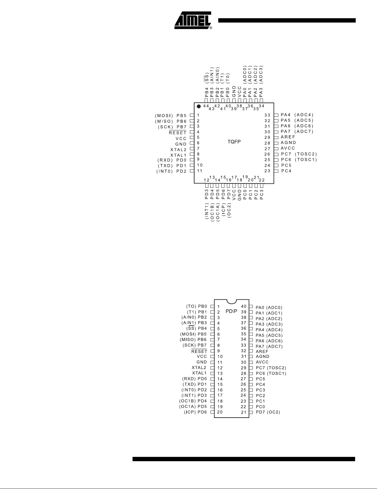
Pin Configurations
(SDA)
(SCL)
(SDA)
(SCL)
2
ATmega163(L)
1142E–AVR–02/03
Page 3
ATmega163(L)
Description The ATmega163 is a low-power CMOS 8-bit microcontroller based on the AVR architec-
ture. By executing powerful instructions in a single clock cycle, the ATmega163
achieves throughputs approaching 1 MIPS per MHz allowing the system designer to
optimize power consumption versus processing speed.
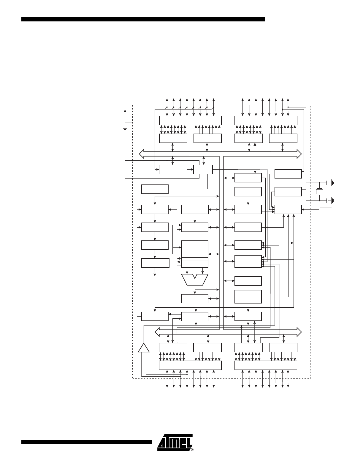
Block Diagram Figure 1. Block Diagram
PA0 - PA7
VCC
PC0 - PC7
GND
AVCC
AGND
AREF
DATA REGISTER
INTERNAL
REFERENCE
PROGRAM
COUNTER
PROGRAM
FLASH
INSTRUCTION
REGISTER
INSTRUCTION
DECODER
CONTROL
LINES
PORTA DRIVERS
PORTA
ANALOG MUX
REG. PORTA
STACK
POINTER
SRAM
GENERAL
PURPOSE
REGISTERS
X
Y
Z
ALU
STATUS
REGISTER
DATA DIR.
ADC
8-BIT DATA BUS
PORTC DRIVERS
DATA REGISTER
PORTC
2-WIRE SERIAL
INTERFACE
INTERNAL
OSCILLATOR
WATCHDOG
TIMER
MCU CONTROL
REGISTER
TIMER/
COUNTERS
INTERRUPT
UNIT
EEPROM
INTERNAL
CALIBRATED
OSCILLATOR
DATA DIR.
REG. PORTC
OSCILLATOR
OSCILLATOR
TIMING AND
CONTROL
XTAL1
XTAL2
RESET
1142E–AVR–02/03
PROGRAMMING
LOGIC
DATA REGISTER
+
ANALOG
COMPARATOR
PORTB
SPI
REG. PORTB
PORTB DRIVERS
PB0 - PB7
DATA DIR.
UART
DATA REGISTER
PORTD
PORTD DRIVERS
PD0 - PD7
DATA DIR.
REG. PORTD
The AVR core combines a rich instruction set with 32 general purpose working registers.
All the 32 re gist ers ar e d irect ly co nnec ted t o t he Ari thme tic Logi c Un it (A LU), allow ing
two independent registers to be accessed in one single instruction executed in one clock
3
Page 4

cycle. The resulting architecture is more code efficient while achieving throughputs up to
ten times faster than conventional CISC microcontrollers.
The ATmega163 provides t he f ollowing featu res: 16K by tes of In-Sy stem Se lf-Programmable Flash, 512 bytes EEPROM, 1024 bytes SRAM, 32 general purpose I/O lines, 32
general purpose worki ng regist ers, three flexib le Timer/Cou nters with compa re modes,
internal and external interrupts, a byte oriented Two-wire Serial Interface, an 8-cha nnel,
10-bit ADC, a program mable Wat chdog Ti mer with internal Osci llator, a program mable
serial UART, an SPI serial port, and four software selectable power saving modes. The
Idle mode stops the CPU while allowing the SRAM, Timer/Counters, SPI port, and interrupt system to continue functioning. The Power-down m ode sa ves the register contents
but freezes the Oscillator, disabling all other chip functions until the next interrupt or
Hardware Reset. In Power-save mode , the asynchrono us Timer Oscillator cont inues to
run, allow ing the u ser to m aintai n a time r base whi le the rest of the device i s slee ping.
The ADC No ise Redu ction mo de stop s the CP U and a ll I/O mo dules exce pt asy nchronous timer and ADC, to minimize switching noise during ADC conversions.
The On-chip ISP Flash can be programmed through an SPI serial interface or a conventional programmer. By installing a Self-Programming Boot Loader, the microcontroller
can be updated within the applica tion without any extern al comp onents. The Boot P rogram can use any interface to download the application program in the Application Flash
memory. By combining an 8-bit CPU with In-System Self-Programmable Flash on a
monolithic chip, the Atmel ATmega163 is a powerful microcontroller that provides a
highly flexible and cost effective solution to many embedded control applications.
The ATmega163 AVR is supported with a full suite of program and system development
tools i nclud ing: C comp ile rs, m acro a sse mbl ers, progra m de bugg er /simu lators , In -Circuit Emulators, and evaluation kits.
Pin Descript i on s
VCC Digital supply voltage. GND Digital ground. Port A (PA7..PA0) Port A serves as the analog inputs to the A/D Converter.
Port A also serves as an 8-bit bi-directional I/O port, if the A/D Converter is not used.
Port pins can provide internal pull-up resistors (selecte d for eac h bit). The P ort A output
buffers can sink 20mA and can drive LED displ ays directly. When pi ns PA0 to PA 7 are
used as inputs and are externally pulled low, they will source current if the internal pullup resistors are activated. The Port A pins are tristated when a reset condition becomes
active, even if the clock is not running.
Port B (PB7..PB0) Port B is an 8-bit bi-directional I/O port with internal pull -up resistors (sele cted for each
bit). The Port B output buffers can sink 20 mA. As in puts, P ort B pins that are ex ternally
pulled low will source current if the pull-up resistors are activated. Port B also serves the
functions of va rious sp eci al feat ures of th e ATm ega83 /163 as list ed on page 117 . T he
Port B pins are tristated when a reset condition becomes active, even if the clock is not
running.
Port C (PC7..PC0) Port C is an 8-bit bi-directional I/O port with internal pull-up resistors (selected fo r each
bit). The Port C output buffers can sink 20 mA. As inputs, Port C pins that are externally
pulled low wi ll sou rce curren t if the p ull-u p resist ors are a ctivate d. The P ort C pins a re
tristated when a reset condition becomes active, even if the clock is not running.
4
ATmega163(L)
1142E–AVR–02/03
Page 5

ATmega163(L)
Port C also serves the f unc tions of various special features of t he A Tmega163 as listed
on page 124.
Port D (PD7..PD0) Port D is an 8-b it bidi rectiona l I/O port with inte rnal pu ll-up resis tors (sel ected for eac h
bit). The Port D output buffers can sink 20 mA. As inputs, Port D pins that are externally
pulled low will source current if the pull-up resistors are activated. Port D also serves the
functions of various special features of the AT m ega163 as listed on page 128. The Port
D pins are tristated when a reset condition becomes active, even if the clock is not
running.
RESET
Reset input. A low leve l on th is pin for m ore than 50 0 ns w ill generat e a Rese t, eve n if
the clock is not running. Shorter pulses are not guaranteed to generate a Reset.
XTAL1 Input to the inverting Oscillator amplifier and input to the internal clock operating circuit. XTAL2 Output from the inverting Oscillator amplifier. AVCC This is the supply vol tage pin for P ort A an d the A/D Conve rter. I t should b e extern ally
connected to V
nected to V
, even if the ADC is not used. If the ADC is used, it should be con-
CC
through a low-pass filter. See page 105 for details on operation of the
CC
ADC.
AREF AREF is the analog reference input pin for the A/D Converter. For ADC operations, a
voltage in the range 2.5V to AVCC can be applied to this pin.
AGND Analog ground. If the board has a separate analog ground plane, this pin should be con-
nected to this ground plane. Otherwise, connect to GND.
Clock Options The device has the following clock source options, selectable by Flash Fuse bits as
shown:
Table 1. Device Clocking Options Select
Device Clocking Option CKSEL3..0
External Crystal/Ceramic Resonator 1111 - 1010
(1)
External Low-frequency Crystal 1001 - 1000
External RC Oscillator 0111 - 0101
Internal RC Oscillator 0100 - 0010
External Clock 0001 - 0000
Note: 1. “1” means unprogrammed, “0” means programmed.
The various choices for each clocking option give different start-up times as shown in
Table 5 on page 25.
Internal RC Oscillator The internal RC Oscillator option is an On-chip Oscillator running at a fixed frequency of
nominally 1 MHz . If sel ected, the device can operate with no external com pone nts. The
device is shipped with this option selected. See “EEPROM Read/Write Access” on page
62 for information on calibrating this Oscillator.
1142E–AVR–02/03
5
Page 6
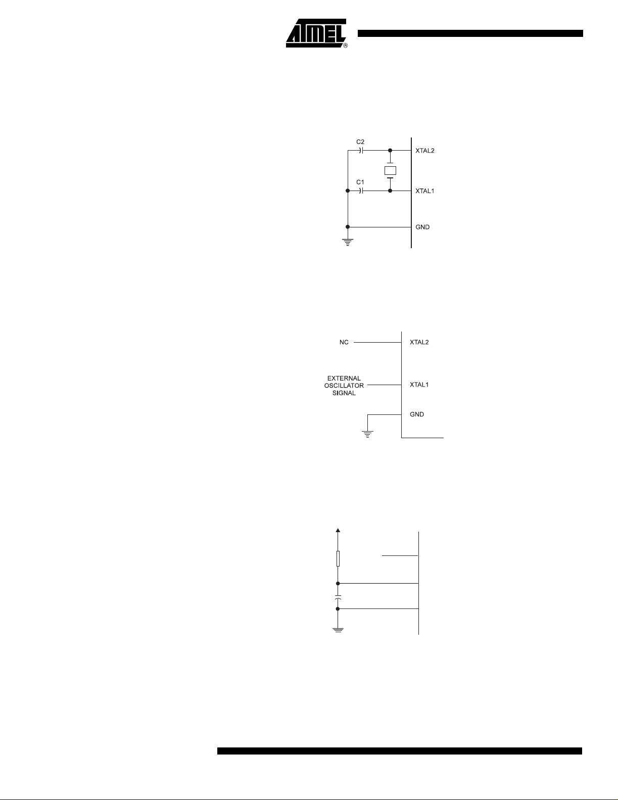
Crystal Oscillator XTAL1 and XTAL2 are input and output, respectively, of an inverting amplifier which can
be configured for use as an On-chip Oscillator, as shown in Figure 2. Either a quartz
crystal or a ceramic resonator may be used.
Figure 2. Oscillator Connections
External Clock To drive the device from an ext ernal clock s ource, XT AL 1 should b e driven as shown i n
Figure 3.
Figure 3. External Clock Drive Configuration
External RC Oscillator For timing insensitive app lications, the ex ternal RC configuration shown i n Figure 4 c an
be used. For details on how to choose R and C, see Table 64 on page 162.
Figure 4. External RC C onfigurati on
V
CC
R
C
NC
XTAL2
XTAL1
GND
Timer Oscillator For the Timer Oscillator pins, TOSC1 and TOSC2, the crystal is connect ed directly
between the pins. No external capacitors are needed. The Oscillator is optimized for use
with a 32,768 Hz watch crystal. Appl ying an e xternal cloc k source to the T OSC1 pin is
not recommended.
6
ATmega163(L)
1142E–AVR–02/03
Page 7

ATmega163(L)
Architectural Overview
The fast-access Register File concept contains 32 x 8-bit general purpose working registers with a single clock cycle access time. This means that during one single clock
cycle, one Arithmetic Logic Unit (ALU) operation is executed. Two ope rands are output
from the Register File, the operation is executed, and the result is stored back in the
Register File – in one clock cycle.
Six of the 32 registers can be used as three 16-bits indirect address register pointers for
Data Spa ce addressi ng – enabling efficient address cal culations. One of the thre e
address pointers is also used as the address pointer for look-up tables in Flash Program
memory. These added function registers are the 16-bits X-, Y-, and Z-register.
The ALU supports arithmetic and logic operat ions between registers or between a c onstant an d a regi ster. Si ng le regis ter ope ratio ns ar e also exec uted in the AL U. Figure 5
shows the ATmega163 AVR Enhanced RISC microcontroller architecture.
In addition to the register operation, the conventional Memory Addressing modes can be
used on the Register File as well. This is enabled by the fact that the Register File is
assigned the 32 lowest Data Space addresses ($00 - $1F), allowing them to be
accessed as though they were ordinary memory locations.
The I/O Memory s pace cont ains 64 a ddresse s for CPU peri pheral func tions as Con trol
Registers, Timer/Counters, A/D-converters, and other I/O functions. The I/O Memory
can be accessed directly, or as the Data Space locations following those of the Register
File, $20 - $5F.
1142E–AVR–02/03
7
Page 8
Figure 5. The ATmega163
8K X 16
Program
Memory
AVR
RISC Architecture
Program
Counter
Data Bus 8-bit
Status
and Control
Interrupt
Unit
SPI
Unit
Instruction
Register
Instruction
Decoder
Control Lines
Direct Addressing
Indirect Addressing
32 x 8
General
Purpose
Registrers
ALU
1024 x 8
Data
SRAM
512 x 8
EEPROM
32
I/O Lines
Serial
UART
Two-wire Serial
Interface
8-bit
Timer/Counter
16-bit
Timer/Counter
with PWM
8-bit
Timer/Counter
with PWM
Watchdog
Timer
A/D Converter
Analog
Comparator
The AVR use s a Harvard architecture concept – with separate me mories and bus es f or
program and data. The Program memory is executed with a two stage pipeline. While
one instru ction is bei ng execu ted, the nex t inst ruction i s pre -fetche d from the P rogram
memory. This concept enables instructions to be executed in every clock cycle. The
Program memory is In-System Re-programmable Flash memory.
With the jump and call instructions, the whole 8K word address space is directly
accessed. Most AVR instructions have a single 16-bit word format. Every program
memory address contains a 16- or 32-bit instruction.
Program Flash memory space is divided in two sections, the Boot Program section (256
to 2,048 bytes, see page 134) and the A ppli cation P rogram se ction. Bot h sec tions hav e
dedicated Lo ck bits for write a nd re ad/write pr otection . The SPM in struct ion that wr ites
into the Application Flash memory section is allowed only in the Boot Program section.
During interrupts and subroutine calls, the return address Program Counter (PC) is
stored on the Stack. The Stack is effectively allocated in the general data SRAM, and
consequently the S tack si ze is onl y limited by the total SRAM size and the usage of t he
SRAM. All user programs mus t initialize the SP in the reset routine (before sub routines
or interrupts are execu ted). T he 11-bi t Stack Pointer S P is read/ write acc essibl e in the
I/O s pace.
8
ATmega163(L)
1142E–AVR–02/03
Page 9

ATmega163(L)
The 1,024 bytes data SRAM can be easily accessed through the five different addressing modes supported in the AVR architecture.
The memory spaces in the AVR
A flexible inte rrupt modu le has its Cont rol Reg isters in the I/O space wi th an addi tional
Global Interrupt Enable bit in the Status Register. All interrupts have a separate Interrupt
Vector in the Interrupt Vector table at the beginni ng of the Program m emory. The interrupts have priority in accordance with their Inte rrupt Vector position. The lower the
Interrupt Vector address, the higher the priority.
Figure 6. Memory Maps
architecture are all linear and regular memory maps.
Program Memory
$0000
Application Flash Section
Boot Flash Section
$1FFF
1142E–AVR–02/03
9
Page 10
The General Purpose Register File
Figure 7 shows the structure of the 32 general purpose working registers in the CPU.
Figure 7. AVR CPU General Purpose Working Registers
7 0 Addr.
R0 $00
R1 $01
R2 $02
…
R13 $0D
General R14 $0E
Purpose R15 $0F
Working R16 $10
Registers R17 $11
…
R26 $1A X-register Low Byte
R27 $1B X-register High Byte
R28 $1C Y-register Low Byte
R29 $1D Y-register High Byte
R30 $1E Z-register Low Byte
R31 $1F Z-register High Byte
All the register operating instructions in the instruction set have direct and single cycle
access to all registers. The only excepti on is the five con stant arithme tic and logic
instructions SBCI, SU BI, CPI, AND I, and ORI betwee n a constan t and a regis ter, and
the LDI instruction for load immediate constant data. These instructions apply to the
second half of the registers in the Register File – R16..R31. The general SBC, SUB, CP,
AND, and OR and all other operations between two registers or on a single register
apply to the entire Register File.
The X-register, Y-register, and Z-register
As shown in F igu re 7, each register i s a lso assigned a data memory address, m appin g
them directly into the first 32 locations of the user Data Space. Although not being physically implemented as SRAM locations, this memory organization provides great
flexibility in access of the registers, as the X-, Y-, and Z-registers can be set to index any
register in the file.
The registers R26..R31 have some added functions to their general purpose usage.
These registers are address pointers for indirect addressing of the Data Space. The
three indirect address registers X, Y, and Z are defined as:
Figure 8. The X-, Y-, and Z-registers
15 XH XL 0
X - register 7 0 7 0
R27 ($1B) R26 ($1A)
15 YH YL 0
Y - register 7 0 7 0
R29 ($1D) R28 ($1C)
15 ZH ZL 0
Z - register 7 0 7 0
R31 ($1F) R30 ($1E)
10
ATmega163(L)
1142E–AVR–02/03
Page 11
ATmega163(L)
In the diff erent addr essi ng mo des t hese ad dre ss re gister s have f unct ions a s fixe d displacement, automatic increment and decrement (see the descriptions for the different
instructions).
The ALU – Arithmetic Logic U nit
The high-performance AVR ALU operates in direct connection with all the 32 general
purpose working reg isters. Within a single clock cycl e, ALU operations between registers in the Re gis ter File are exe cuted . The A LU ope rati ons are d ivided int o three m ain
categories – arithmetic, logical, and bit-functions. ATm ega163 also provi des a powerful
multiplier sup porting both s igne d/unsigned mult iplication an d fractiona l form at. See the
Instruction Set section for a detailed description.
The In-System SelfProgrammable Flash
Program Memory
The ATme ga163 c ontains 16K bytes On -chip In-Sy stem Self-Pro gramm able Flas h
memory for program storage. Since all instructions are 16- or 32-bit words, the Flash is
organized as 8K x 16. The Flash Program memory space is divided in two sections,
Boot Program section and Application Progra m section.
The Flash memory has an endurance of at least 1,000 write/erase cycles. The
ATmega163 Prog ram Count er (PC) is 13 bits wide, thus address in g the 8,192 Program
Memory locations. The operation of Boot Program section and associated Boot Lock
bits for software protection are described in detail on page 134. See also page 154 for a
detailed description on Flash data serial downloading.
Constant tables can be allocated within the entire Program Memory address space (see
the LPM – Load Program Memory instruction description).
See also page 12 for the different Program Memory Addressing modes.
The SRAM Data Memory F igure 9 shows how the ATmega163 SRAM Mem ory is organized.
Figure 9. SRAM Organization
Register File
R0
R1
R2
...
R29
R30
R31
I/O Registers
$00
$01
$02
...
$3D
$3E
$3F
Data Address Space
$0000
$0001
$0002
...
$001D
$001E
$001F
$0020
$0021
$0022
...
$005D
$005E
$005F
Internal SRAM
$0060
$0061
...
$045E
$045F
1142E–AVR–02/03
11
Page 12
The lower 1,120 Data Memory locations address the Register File, the I/O Memory, and
the internal data SR AM. The first 96 loc ations addres s the Register F ile + I/O Memory,
and the next 1,024 locations address the internal data SRAM.
The five different addressing modes for the data memory cover: Direct, Indirect with Displacement, In direc t, Indirect with Pr e-decr emen t, and Ind irect w ith Pos t-increm ent. In
the Register F ile, registers R26 t o R31 feature the indirect Addre ssing Pointer
Registers.
The direct addressing reaches the entire data space.
The Indirect with Displacement mode features a 63 address locations reach from the
base address given by the Y- or Z-register.
When using register indirect addressing modes with automatic pre-decrement and post-
increment, the address registers X, Y, and Z are decremented and incremented.
The 32 general purpose working registers, 64 I/O Registers, and the 1,024 bytes of
internal data S RAM i n the ATme ga163 are a ll acce ssib le throu gh all thes e addre ssin g
modes.
The Program and Data Addressing Modes
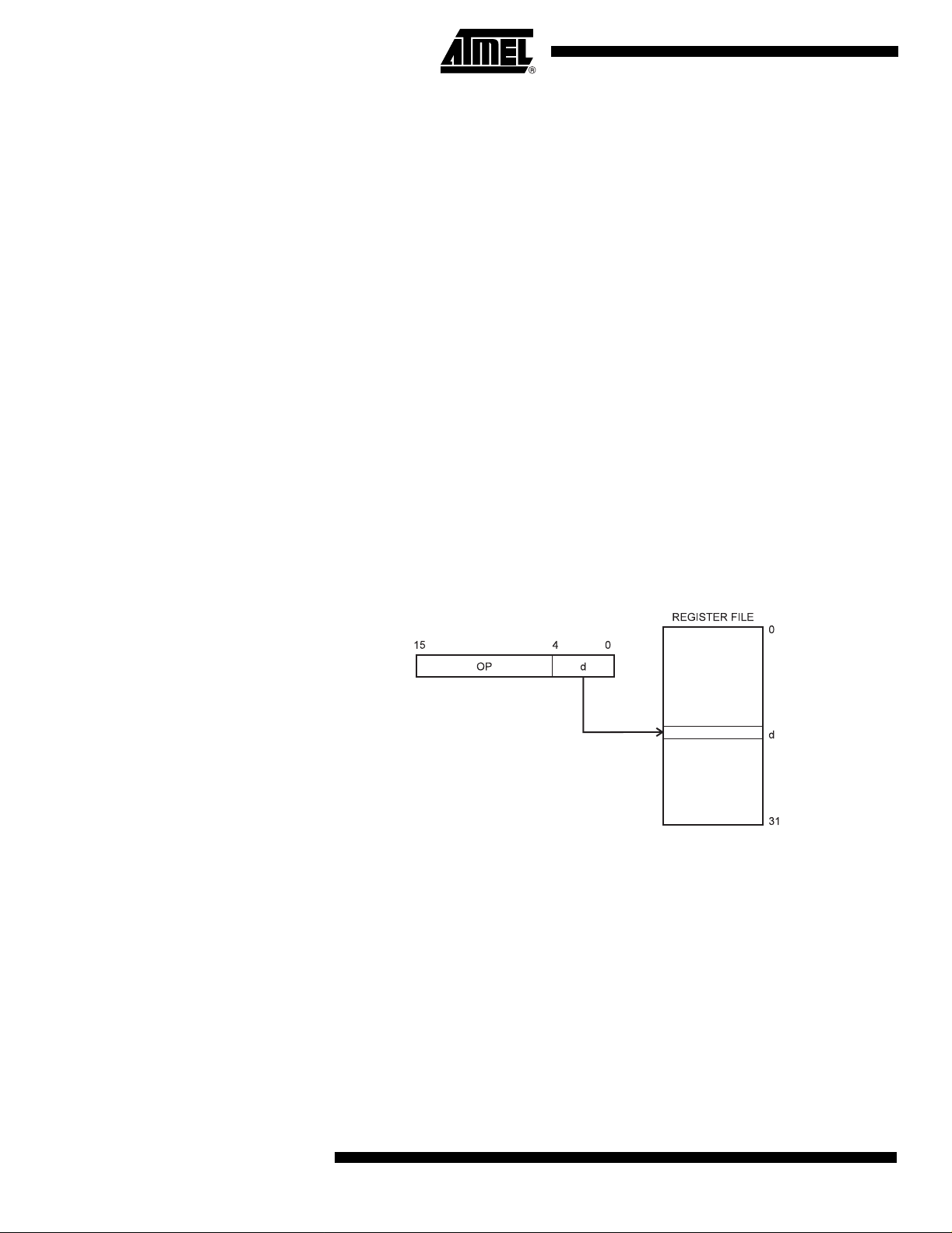
Register Direct, Single Register Rd
The AT meg a163 AVR E nha nce d RIS C mic roco ntro ller s uppor ts po wer ful and effi cient
addressing modes for access to the Program Memory (Flash) and Data Memory
(SRAM, Register File, and I/O Memory). This section des cribes t he different ad dressing
modes supported by the AVR architecture. In the figures, OP means the operation code
part of the instruction word. To simplify, not all figures show the exact location of the
addressing bits.
Figure 10. Direct Single Register Addressing
The operand is contained in register d (Rd).
12
ATmega163(L)
1142E–AVR–02/03
Page 13
ATmega163(L)
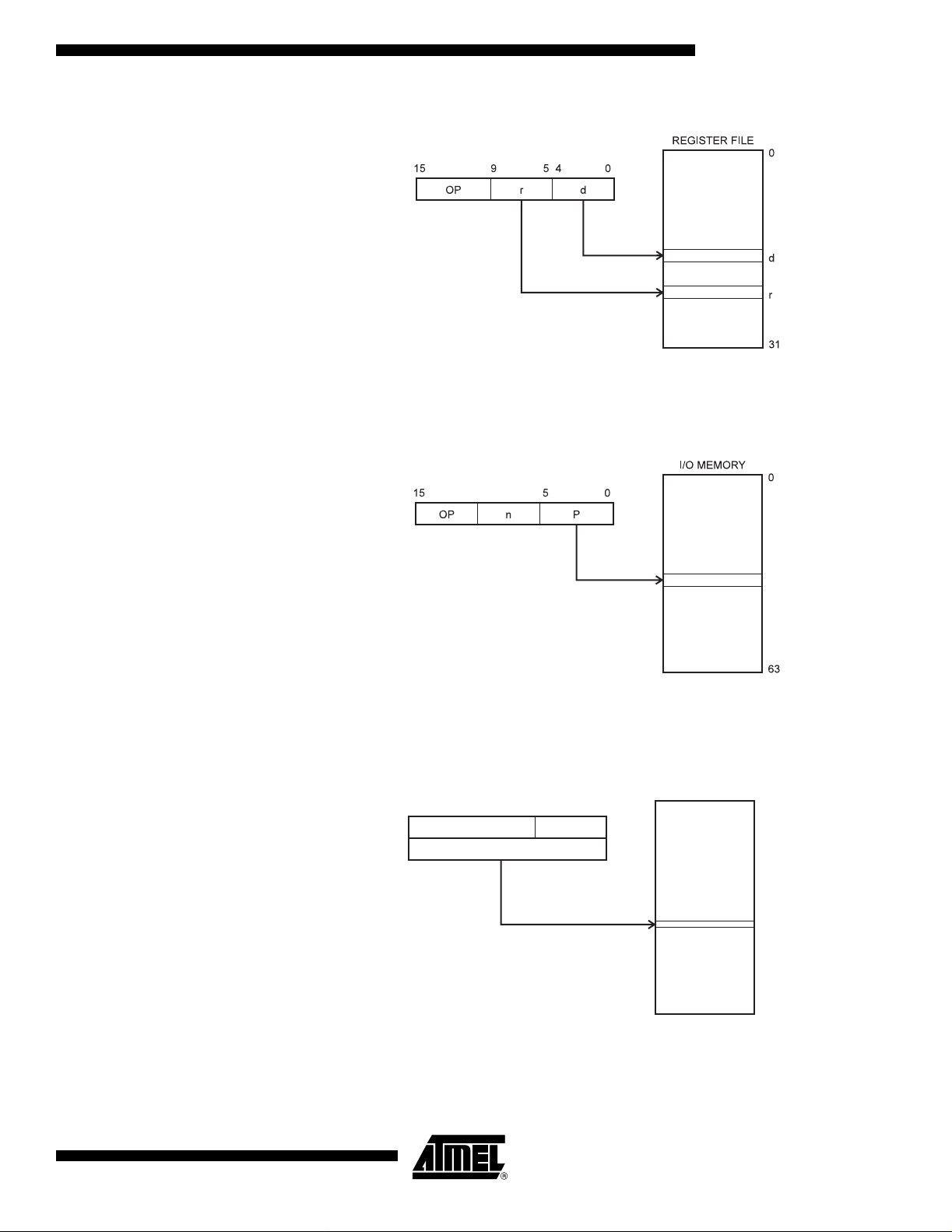
Register Direct, Two Registers
Figure 11. Direct Register Addressing, Two Registers
Rd And Rr
Operand s ar e co ntain ed i n regi ster r (Rr) a nd d (Rd) . Th e resu lt is stor ed i n regis ter d
(Rd).
I/O Direct Figure 12. I/O Direct Addressing
Operand address is contained in 6 bits of the instruction word. n is the destination or
source register address.
Data Direct Figure 13. Direct Data Addressing
31
OP Rr/Rd
16 LSBs
15 0
20 19
A 16-bit Data Address is contained in the 16 LSBs of a two-word instruction. Rd/Rr
specify the destination or source register.
1142E–AVR–02/03
Data Space
16
$0000
$045F
13
Page 14
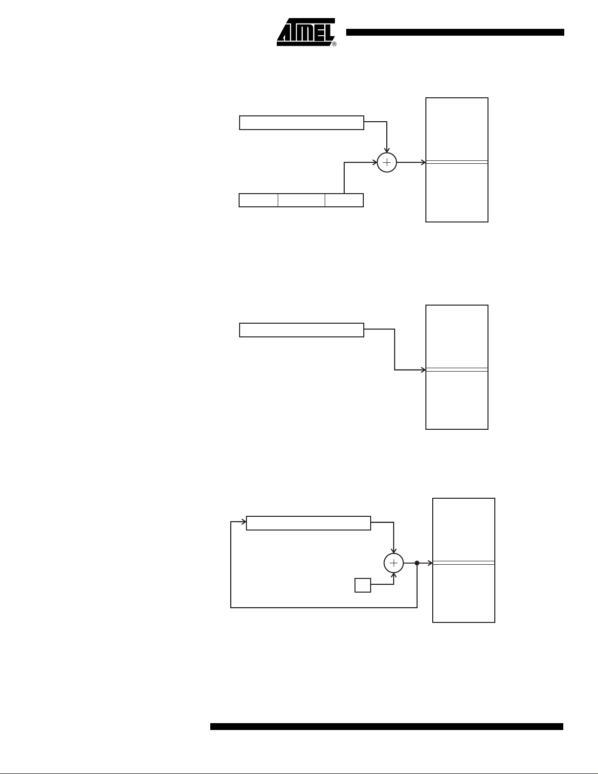
Data Indirect with Displacement
Figure 14. Data Indirect with Displacement
15
Y OR Z - REGISTER
0
Data Space
$0000
15
OP an
Operand address is the result of the Y- or Z-register contents added to the address contained in 6 bits of the instruction word.
Data Indirect Figure 15. Data Indirect Addressing
X, Y OR Z - REGISTER
Operand address is the contents of the X-, Y-, or the Z-register.
05610
$045F
Data Space
015
$0000
$045F
Data Indirect with Predecrement
14
ATmega163(L)
Figure 16. Data Indirect Addressing with Pre-decrement
Data Space
015
X, Y OR Z - REGISTER
-1
$0000
$045F
The X-, Y -, or th e Z-reg ister is decre ment ed be fore the opera tio n. Opera nd address is
the decremented contents of the X-, Y-, or the Z-register.
1142E–AVR–02/03
Page 15
ATmega163(L)
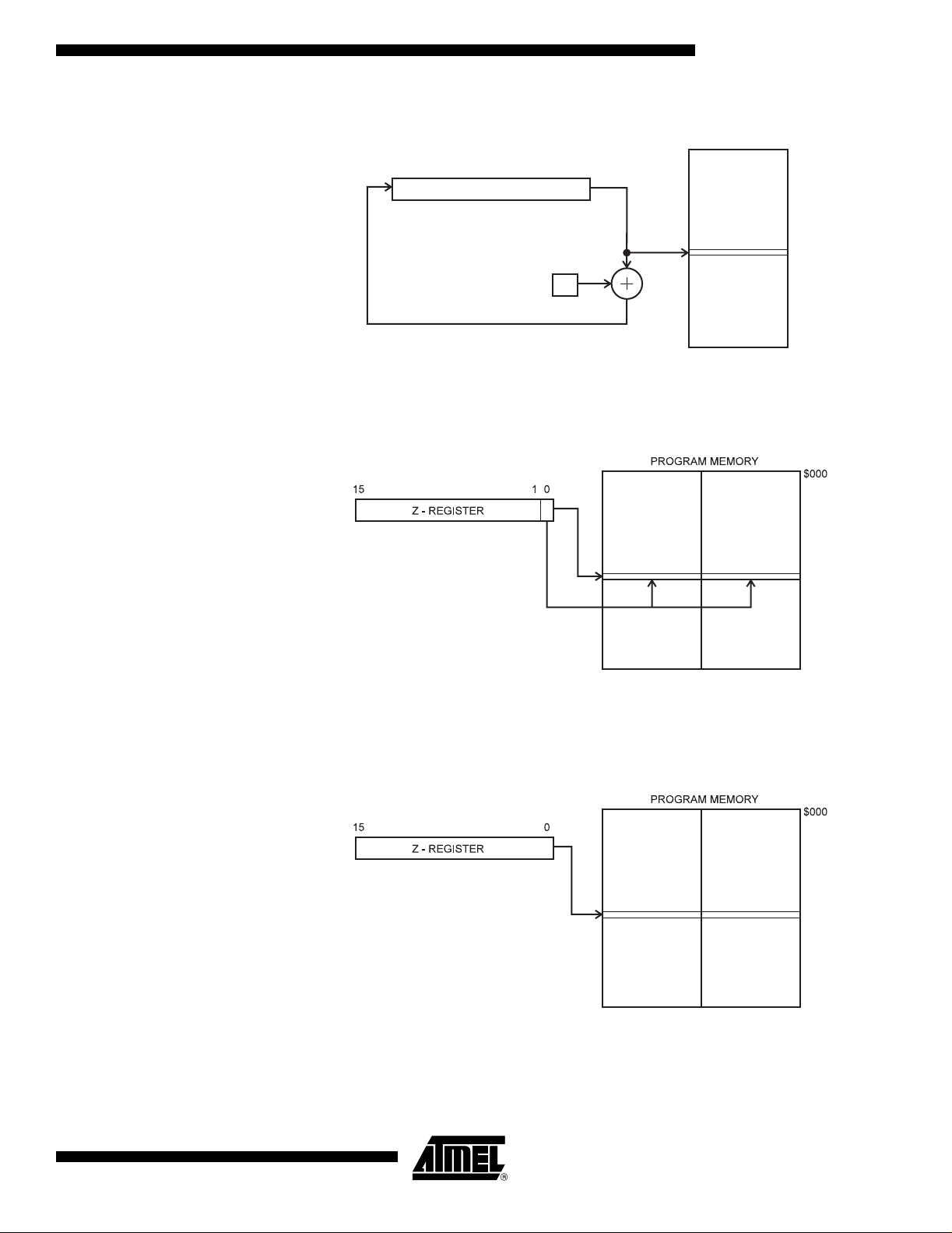
Data Indirect with Postincrement
Constant Addressing Using The LPM and SPM Instructions
Figure 17. Data Indirect Addressing with Post-increment
Data Space
015
X, Y OR Z - REGISTER
1
$0000
$045F
The X-, Y-, or the Z-register is incremented after the operation. Operand address is the
content of the X-, Y-, or the Z-register prior to incrementing.
Figure 18. Code Mem ory C onstant Addressin g
Indirect Program Addressing, IJMP and ICALL
$1FFF
Constant byte address is specified by the Z-register contents. The 15 MSBs select word
address (0 - 8K). For LPM, the LSB selects Low Byte if cleared (LSB = 0) or High Byte if
set (LSB = 1). For SPM, the LSB should be cleared.
Figure 19. Indirect Program Memory Addressing
$1FFF
Program execution continues at address contained by the Z-register (i.e., the PC is
loaded with the contents of the Z-register).
1142E–AVR–02/03
15
Page 16
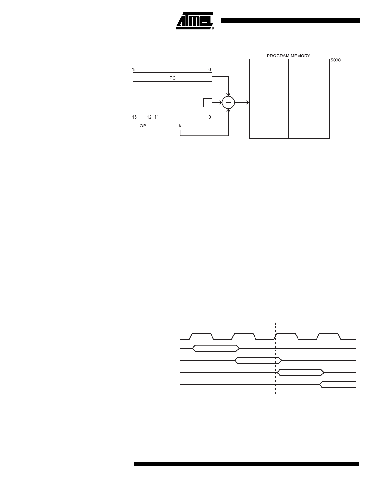
Relative Program Addressing, RJMP and RCALL
Figure 20. Relative Program Memory Addressing
1
$1FFF
Program execution continues at address PC + k + 1.
The relative address k is from -2,048 to 2,047.
The EEPROM Data Memory
Memory Access Times and Instruction Execution Timing
The ATmega163 contains 512 bytes of data EEPROM memory. It is or g anized as a se p arate data space, in which single bytes can be read and written. The EEPROM has an
endurance of at least 100,000 write/erase cycles. The access between the EEPROM
and the CPU is described on page 62 specifying the EEPROM Address Registers, the
EEPROM Data Registe r, and the EEPROM Control Register.
For the SPI data downloading, see page 154 for a detailed description.
This section describes the general ac cess timing co ncepts for in struction ex ecut ion a nd
internal memory access.
The AVR CPU is driven by the System Clock Ø, directly generated from the main Os cillator for the chip. No internal clock division is used.
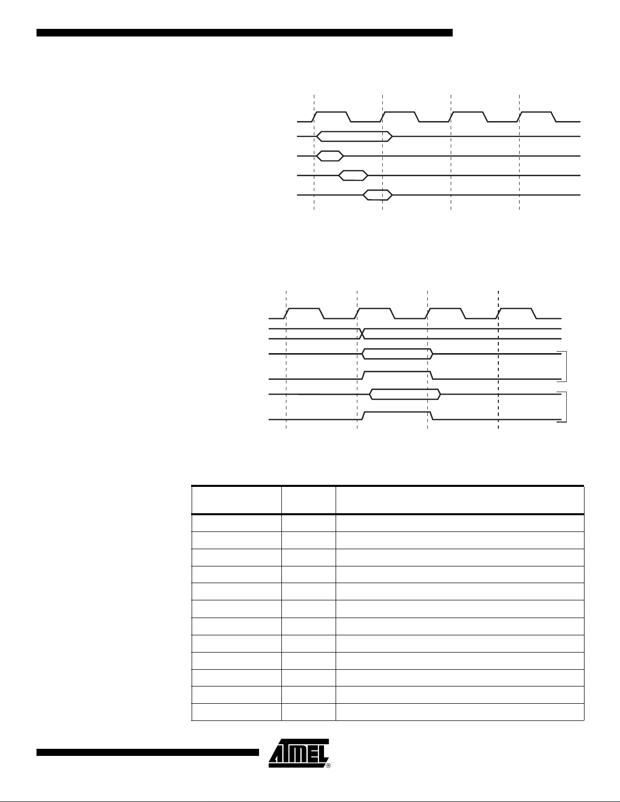
Figure 21 s hows t he pa ralle l instru ctio n fetch es a nd ins truct ion e xecu tions enab led b y
the Harvard architecture and the fast-access Register File concept. This is the basic
pipelining concept to obtain up to 1 MIPS per MHz with the corresponding unique results
for functions per cost, functions per clocks, and functions per power-unit.
Figure 21. The Parallel Instruction Fetches and Instruction Executions
T1 T2 T3 T4
System Clock Ø
1st Instruction Fetch
1st Instruction Execute
2nd Instruction Fetch
2nd Instruction Execute
3rd Instruction Fetch
3rd Instruction Execute
4th Instruction Fetch
16
Figure 22 shows the internal timing conc ept f or the Regist er F ile. In a singl e clock cy cle
an ALU operation using two register operands is executed, and the result is stored back
to the destination register.
ATmega163(L)
1142E–AVR–02/03
Page 17
ATmega163(L)
Figure 22. Single Cycle ALU Operation
T1 T2 T3 T4
System Clock Ø
Total Execution Time
Register Operands Fetch
ALU Operation Execute
Result Write Back
The internal data SR AM access is pe rformed in tw o System Cl ock cycles as des cribed
in Figure 23.
Figure 23. On-chip Data SRAM Access Cycles
T1 T2 T3 T4
System Clock Ø
Address
Data
WR
Data
RD
Prev. Address
Address
I/O Memory The I/O space definition of the ATmega163 is shown in the following table:
Table 2. ATmega163 I/O Space
I/O Address
(SRAM Address) Name Function
$3F ($5F) SREG Status REGister
$3E ($5E) SPH Stack Pointer High
$3D ($5D) SPL Stack Pointer Low
$3B ($5B) GIMSK General Interrup t MaSK Regis ter
$3A ($5A) GIFR General Interrupt Flag Register
$39 ($59) TIMSK Timer/Counter Int errupt MaSK Register
$38 ($58) TIFR Timer/Counter Interrupt Flag Register
(1)
Write
Read
1142E–AVR–02/03
$37 ($57) SPMCR SPM Control Register
$36 ($56) TWCR Two-wire Serial Interface Control Register
$35 ($55) MCUCR MCU general Control Register
$34 ($54) MCUSR MCU general Status Register
$33 ($53) TCCR0 Timer/Counter0 Cont rol Register
17
Page 18

Table 2. ATmega163 I/O Space (Continued)
I/O Address
(SRAM Address) Name Function
$32 ($52) TCNT0 Timer/Counter0 (8-bit)
$31 ($51) OSCCAL Oscillator Calibration Register
$30 ($50) SFIOR Special Function I/O Register
$2F ($4F) TCCR1A Timer/Counter1 Control Register A
$2E ($4E) T CCR1B Timer/Counter1 Control Register B
$2D ($4D) TCNT1H Timer/Counter1 Hig h-byte
$2C ($4C) TCNT1L Timer /Counter1 Low-byte
$2B ($4B) OCR1AH Timer/Counter1 Output Compare Register A High-byte
$2A ($4A) OCR1AL Timer/Counter1 Output Compare Register A Low-byte
$29 ($49) OCR1BH Timer/Counter1 Output Compare Regis ter B High-byte
$28 ($48) OCR1BL Timer/Counter1 Output Compare Regis ter B Low-byte
$27 ($47) ICR1H T/C 1 Input Capture Register High-byte
$26 ($46) ICR1L T/C 1 Input Capture Register Low-byte
$25 ($45) TCCR2 Timer/Counter2 Cont rol Register
$24 ($44) TCNT2 Timer/Counter2 (8-bit)
(1)
$23 ($43) OCR2 Timer/Coun ter 2 O utput Compare Register
$22 ($42) ASSR Asynchronous Mode Status Regi ster
$21 ($41) WDTCR Watchdog Timer Control Register
$20 ($40) UBRRHI UART Baud Rate Register High-byte
$1F ($3F) EEARH EEPROM Address Register High-byte
$1E ($3E) EEARL EEPROM Address Register Low-byte
$1D ($3D) EEDR EEPROM Data Register
$1C ($3C) EECR EEPROM Control Register
$1B ($3B) PORTA Data Register, Port A
$1A ($3A) DDRA Data Direction Regi ster, Port A
$19 ($39) PINA Input Pins, Port A
$18 ($38) PORTB Data Register, Port B
$17 ($37) DDRB Data Direction Register, Port B
$16 ($36) PINB Input Pins, Port B
$15 ($35) PORTC Data Regist er, Port C
$14 ($34) DDRC Data Direction Register, Port C
$13 ($33) PINC Input Pins, Port C
$12 ($32) PORTD Data Regist er, Port D
18
$11 ($31) DDRD Data Direction Register, Port D
$10 ($30) PIND Input Pins, Port D
ATmega163(L)
1142E–AVR–02/03
Page 19

ATmega163(L)
Table 2. ATmega163 I/O Space (Continued)
I/O Address
(SRAM Address) Name Function
$0F ($2F) SPDR SPI I/O Data Register
$0E ($2E) SPSR SPI Status Register
$0D ($2D) SPCR SPI Control Register
$0C ($2C) UDR UART I/O Data Register
$0B ($2B) UCSRA UART Control and Status Register A
$0A ($2A) UCSRB UART Control and Status Register B
$09 ($29) UBRR UART Baud Rate Register
$08 ($28) ACSR Analog Comparator Control and Status Register
$07 ($27) ADMUX ADC Multiplexer Selec t Regi ster
$06 ($26) ADCSR ADC Control and Status Regist er
$05 ($25) ADCH ADC Data Register High
$04 ($24) ADCL ADC Data Register Low
$03 ($23) TWDR Two-wire Serial Interface Data Register
$02 ($22) TWAR Two-wire Serial Interface (Slave) Address Register
$01 ($21) TWSR Two-wire Ser ial Interface Status Regist er
(1)
$00 ($20) TWBR Two-wire Ser ial Interface Bit Rate Register
Note: 1. Reserved and unused locations are not shown in the table.
All ATmega163 I /Os and peripheral s are place d in the I/O space. The I/O locatio ns are
accessed by the IN and OUT instructions, transferring data between the 32 general purpose working registers and the I/O space. I/O Registers within the address range $00 -
$1F are directly bit-accessible using the SBI and CBI instructions. In these registers,
the value of single bits can be checked by using the SBIS and SB IC instructions. Refer
to the instruction set chapter for more details. When using the I/O specific commands IN
and OUT, the I/O addresses $00 - $3F must be used. When addressing I/O Registers as
SRAM, $ 20 mu st be a dded to t hese ad dre sses. A ll I/O Re giste r address es t hrough out
this document are shown with the SRAM address in parentheses.
For compatibility with future devices, reserved bits should be written to zero if accessed.
Reserved I/O memory addresses should never be written.
Some of the Status Flags are cleared by writing a logical one to them. Note that the CBI
and SBI instru ctio ns wi ll op erate o n a ll bits i n th e I/O Regi ster , writin g a on e b ack in to
any Flag read as set, thus clearing the Flag. The CBI and SBI instructions work with registers $00 to $1F only.
The I/O and Peripherals Control Registers are explained in the following sections.
1142E–AVR–02/03
19
Page 20

The Status Register – SREG The
Bit 76543210
$3F ($5F) I THSVNZCSREG
Read/Write R/W R/W R/W R/W R/W R/W R/W R/W
Initial Value00000000
• Bit 7 – I: Global Interrupt Enable
The Glob al Inte rrupt En able b it must be set (on e) for the inte rrupts to be enab led. The
individu al i nterrup t ena ble c on trol is t hen perf orme d in th e In terrupt Ma sk Regi sters. If
the Global Interrupt Enable Register is cleared (zero), none of the interrupts are enabled
independent of the values of th e Interrupt Ma sk Registers. The I-bit is cleared by hardware after an interrupt ha s occurred, a nd is set by the RETI in struction to e nable
subsequent interrupts.
• Bit 6 – T: Bit Copy Storage
The Bit Co py instruc tions B LD (Bi t LoaD ) and BS T (Bit S Tore ) use th e T-bit a s sourc e
and destination for the operated bit. A bit from a register in the Register File can be copied into T by the BST instruction, and a bit in T can be copied into a bit in a register in the
Register File by the BLD instruction.
• Bit 5 – H: Half Carry Flag
The Half Carry Flag H indicates a half carry in some arithmetic operations. See the
Instruction Set Description for detailed information.
AVR
Status Register – SREG – at I/O space location $3F ($5F) is defined as:
• Bit 4 – S: Sign Bit, S = N
⊕ V
The S-bit is always an exclusive or between the Negative Flag N and the Two’s Complement Overflow Flag V. See the Instruction Set Description for detailed information.
• Bit 3 – V: Two’s Complement Overflow Flag
The Two ’s Com pleme nt O verf low Flag V su ppor ts t wo’s comp lem ent arith meti cs. S ee
the Instruction Set Description for detailed information.
• Bit 2 – N: Negative Flag
The Negative Flag N indicates a negative result in an arithmetic or logic operation. See
the Instruction Set Description for detailed information.
• B i t 1 – Z: Zer o Flag
The Zero Flag Z indicates a zero result in an arithmetic or logic op eration. See the
Instruction Set Description for detailed information.
• Bit 0 – C: Carry Flag
The Carry Flag C indicates a carry in an ari thmetic or logic operation. See the Instruction
Set Description for detailed information.
Note that the Status Register is not automatically stored wh en entering an in terrupt routine and restored when returning from an interrupt routine. This must be handled by
software.
20
ATmega163(L)
1142E–AVR–02/03
Page 21
ATmega163(L)
The Stack Pointer – SP The ATmega163 Stack Pointer is implemented as two 8-bit registers in the I/O space
location s $ 3E ($5E) an d $3 D ( $5D). As the A Tme g a163 data mem ory ha s $46 0 lo cations, 11 bits are used.
Bit 151413121110 9 8
$3E ($5E) – – – – – SP10 SP9 SP8 SPH
$3D ($5D) SP7 SP6 SP5 SP4 SP3 SP2 SP1 SP0 SPL
76543210
Read/Write R R R R R R/W R/W R/W
R/W R/W R/W R/W R/W R/W R/W R/W
Initial Value00000000
00000000
The Stack Pointer poi nts to the dat a S RA M Stack area where the Subrout ine and Interrupt Stacks are located. This Stack space in the data SRAM must be defined by the
program before any sub routine cal ls are executed or in terrupts are enabl ed. The Stack
Pointer must be set to point above $60. The Stack Pointer is decremented by one when
data is pushed ont o the Stack with the PUSH instruc tion, and it is dec remen ted by two
when the return address is pushed onto the Stack with subroutine call and interrupt. The
Stack Pointer is incremented by one when data is popped from the Stack with the POP
instruction, and it is incremented by two when data is popped from the Stack with return
from subroutine RET or return from interrupt RETI.
Reset and Interrupt Handling
The ATmega163 provides 17 different interrupt sources. Thes e interrupts and the separate Res et Vect or, ea ch have a separ ate Prog ram Vec tor in th e Prog ram Mem ory
space. All interrupts are assigned individual enable bits which must be set (one)
together with the I-bit in the Status Register in order to enable the interrupt.
The lowe st ad dres ses in the Pro gram M emo ry sp ace are au toma ticall y def ined as th e
Reset and Interrupt Vectors. Th e complete list of ve ctors is shown in Table 3. Th e list
also determines the priority level s of the different interrupts. The lower the add ress th e
higher is the priority level. RESET has the highe st priority, and next is INT 0 – the E xternal Interrupt Request 0, etc.
Table 3. Reset and Interrupt Vectors
Program
Vector No.
1 $000
2 $002 INT0 External Interrupt Request 0
3 $004 INT1 External Interrupt Request 1
4 $006 TIMER2 COMP Timer/Counter2 Compar e Ma tch
5 $008 TIMER2 OVF Timer/Counter2 Overflow
6 $00A TIMER1 CAPT Timer/Counter1 Capture Event
7 $00C TIMER1 COMPA Timer/Counter1 Compare Match A
Address Source Interrupt Definition
(1)
RESET
External Pin, Power -on Reset, Brown-out
Reset and Watchdog Reset
1142E–AVR–02/03
8 $00E TIMER1 COMPB Timer/Counter1 Compare Match B
9 $010 TIMER1 OVF Timer/Counter1 Overflow
10 $012 TIMER0 OVF Timer/Counter0 Overflow
11 $014 SPI, STC Serial Transfer Co mplete
12 $016 UART, RXC UART, Rx Complete
21
Page 22

Table 3. Reset and Interrupt Vectors (Continued)
Program
Vector No.
Address Source Interrupt Definition
13 $018 UART, UDRE UART Data Register Empty
14 $01A UART, TXC UART, Tx Complete
15 $01C ADC ADC Conversion Complete
16 $01E EE_RDY EEPROM Ready
17 $020 ANA_COMP Analog Comparator
18 $022 TWI Two-wire Serial Interface
Note: 1. When the BOOTRST Fuse is programmed, the device will jump to the Boot Loader
address at reset, see “Boot Loader Support” on page 134.
The most typical and general program setup f or the Reset and Interrupt Vector
Addresses in ATmega163 is:
Address Labels Code Comments
$000 jmp RESET ; Reset Handler
$002 jmp EXT_INT0 ; IRQ0 Handler
$004 jmp EXT_INT1 ; IRQ1 Handler
$006 jmp TIM2_COMP ; Timer2 Compare Handler
$008 jmp TIM2_OVF ; Timer2 Overflow Handler
$00a jmp TIM1_CAPT ; Timer1 Capture Handler
$00c jmp TIM1_COMPA ; Timer1 Compare A Handler
$00e jmp TIM1_COMPB ; Timer1 Compare B Handler
$010 jmp TIM1_OVF ; Timer1 Overflow Handler
$012 jmp TIM0_OVF ; Timer0 Overflow Handler
$014 jmp SPI_STC ; SPI Transfer Complete Handler
$016 jmp UART_RXC ; UART RX Complete Handler
$018 jmp UART_DRE ; UDR Empty Handler
$01a jmp UART_TXC ; UART TX Complete Handler
$01c jmp ADC ; ADC Conversion Complete Interrupt Handler
$01e jmp EE_RDY ; EEPROM Ready Handler
$020 jmp ANA_COMP ; Analog Comparator Handler
$022 jmp TWI ; Two-wire Serial Interface Interrupt Handler
;
$024 MAIN: ldi r16,high(RAMEND) ; Main program start
$025 out SPH,r16 ; Set stack pointer to top of RAM
$026 ldi r16,low(RAMEND)
$027 out SPL,r16
... ... ...
22
ATmega163(L)
1142E–AVR–02/03
Page 23

When the BOO TRS T Fuse is prog ramm ed and the Bo ot sec tion s ize se t to 512 bytes ,
the most ty pical and general program setu p for the Reset and Interrupt Vector
Addresses in ATmega163 is:
Address Labels Code Comments
$002 jmp EXT_INT0 ; IRQ0 Handler
... ... ...
$022 jmp TWI ; Two-wire Serial Interface Interrupt Handler
;
$024 MAIN: ldi r16,high(RAMEND) ; Main program start
$025 out SPH,r16 ; Set stack pointer to top of RAM
$026 ldi r16,low(RAMEND)
$027 out SPL,r16
$028 <instr> xxx
;
.org $1f00
$1f00 jmp RESET ; Reset Handler
Reset Sources T he ATm ega163 has fo ur sources of reset:
• Power-on Reset. The MCU is reset when the supply voltage is below the Power-on
Reset threshold (V
POT
).
• External Reset. The MCU is reset when a low level is present on the RESET
more than 500 ns.
• Watchdog Reset. The MCU is reset when the Watchdog Timer period expires and
the Watchdog is enabled.
• Brown-out Reset. The MCU is reset when the supply voltage V
Brown-out Reset threshold (V
BOT
).
During Reset, all I/O Registers are set to their initial values, and the program starts execution from address $000 (unless the BOOTRST Fuse is programmed, as explained
above). The instruction placed in this address location must be a JMP – absolute jump –
instruction to the reset handling routine. If the program never enables an interrupt
source, the Interrupt Vect ors are not u sed, and reg ular program code c an be pl aced at
these locations. The circuit diagram in Figure 24 shows the Reset Logic. Table 4 and
Table 5 define the timing and electrical parameters of the reset circuitry.
ATmega163(L)
pin for
is below the
CC
1142E–AVR–02/03
23
Page 24
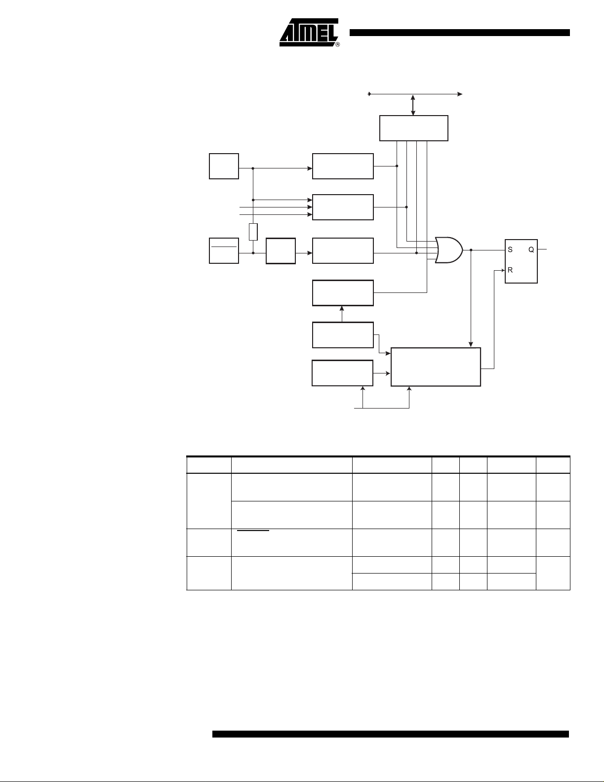
Figure 24. Reset Logic
VCC
Power-on
Reset Circuit
DATA BUS
MCU Status
Register (MCUSR)
BORF
PORF
WDRF
EXTRF
BODEN
BODLEVEL
RESET
100-500kW
SPIKE
FILTER
Brown-out
Reset Circuit
Reset Circuit
Watchdog
Timer
On-chip
RC Oscillator
Clock
Generator
CKSEL[3:0]
CK
Counter Reset
Delay Counters
TIMEOUT
Table 4. Reset Characteristics (VCC = 5.0V)
Symbol Parameter Condition Min Typ Max Units
V
POT
Power-on Reset Thres hold
Voltage (risin g)
1.0 1.4 1.8 V
Internal Reset
24
V
V
Notes: 1. The Power-on Reset will not work unless the supply voltage has been below V
ATmega163(L)
RST
BOT
Power-on Reset Thres hold
Voltage (falling)
(1)
RESET Pin Threshold
Voltage
Brown-out Res et Th reshol d
Voltage
(falling).
0.4 0.6 0.8 V
– – 0.85 V
(BODLEVEL = 1) 2.4 2.7 3.2
(BODLEVEL = 0) 3.5 4.0 4.5
CC
V
V
POT
1142E–AVR–02/03
Page 25

ATmega163(L)
Table 5. Reset Dela y Se lec t io ns
Start-up Time,
V
= 2.7V,
CC
BODLEVEL
Unprogrammed
CKSEL
(2)
(1)
Start-up Time,
V
= 4.0V,
CC
BODLEVEL
Programmed Recommended Usage
(3)
0000 4.2 ms + 6 CK 5.8 ms + 6 CK Ext. Clock, fast rising power
0001 30 µs + 6 CK
(6)
0010
67 ms + 6 CK 92 ms + 6 CK Int. RC Oscillator, slowly rising power
(4)
10 µs + 6 CK
(5)
Ext. Clock, BOD enabled
0011 4.2 ms + 6 CK 5.8 ms + 6 CK Int. RC Oscil lator, fast rising power
0100 30 µs + 6 CK
(4)
10 µs + 6 CK
(5)
Int. RC Oscillator, BOD enabled
0101 67 ms + 6 CK 92 ms + 6 CK Ext. RC Oscillator, slowly risi ng power
0110 4.2 ms + 6 CK 5.8 ms + 6 CK Ext. RC Oscillator, fast ris ing power
0111 30 µs + 6 CK
(4)
10 µs + 6 CK
(5)
Ext. RC Oscillator, BOD enabled
1000 67ms + 32K CK 92 ms + 32K CK Ext. Low-frequency Crystal
1001 67 ms + 1K CK 92 ms + 1K CK Ext. Low-f requency Crystal
1010 67 ms + 16K CK 92 ms + 16K CK Crystal Oscillator, slowly rising power
1011 4.2 ms + 16K CK 5.8 ms + 16K CK Crystal Oscillator, fast rising power
1100 30 µs + 16K CK
(4)
10 µs + 16K CK
1101 67 ms + 1K CK 92 ms + 1K CK
(5)
Crystal Oscillator, BOD enabled
Ceramic Resonator/Ext. Clock, slowly
rising power
1110 4.2 ms + 1K CK 5.8 ms + 1K CK Ceramic Resonator, fast rising power
1111 30 µs + 1K CK
(4)
10 µs + 1K CK
(5)
Ceramic Resonator, BOD enabled
Notes: 1. On power-up, the start -up time is increased with typ. 0. 6 ms.
2. “1” means unprogrammed, “0” means programmed.
3. For possible clock selections, see “Cl ock Options” on page 5.
4. When BODEN is programmed, add 100 µs.
5. When BODEN is programmed, add 25 µs.
6. Default value.
Table 5 shows the Start-up Times from Reset. When the CPU wakes up from Powerdown or Power-sav e, only the clo ck counting part of t he start-up time i s used. The
Watchdog Oscillator is used for timing the real time part of the start-up time. The number
of WDT Oscillator cycles used for each time-out is shown in T a ble 6.
The frequency o f the W at chdog Oscillator is voltage depen dent as shown in the Electrical Characteristics section. The device is shipped with CKSEL = “0010” (Int. RC
Oscillator, slowly rising power).
1142E–AVR–02/03
25
Page 26
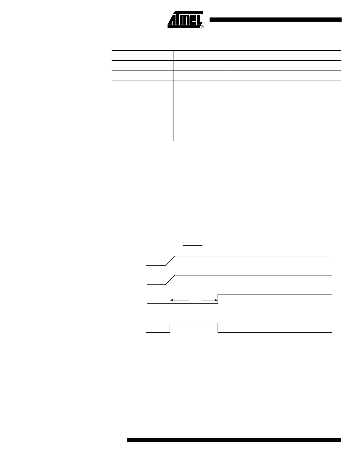
Table 6. Number of Watchdog Osc illa tor C ycl es
(1)
BODLEVEL VCC Condition Time-out Number of Cycles
Unprogrammed 2.7V 30 µs 8
Unprogrammed 2.7V 130 µs 32
Unprogrammed 2.7V 4.2 ms 1K
Unprogrammed 2.7V 67 ms 16K
Programmed 4.0V 10 µs 8
Programmed 4.0V 35 µs 32
Programmed 4.0V 5.8 ms 4K
Programmed 4.0V 92 ms 64K
Note: 1. The Bodlevel Fuse can be used to select start-up times even if the Brown-out Detec-
tion is disabled (BODEN Fuse unprogrammed).
Power-on Reset A Power-on Reset (POR) pulse is generated by an On-chip detection circuit. The detec-
tion level is defined in Table 4. The POR is activated whenever V
is b elo w the
CC
detection level. The POR circuit can be u sed t o trigger the Start-up Reset, as well as t o
detect a failure in supply voltage.
A Power-on Reset (POR) circuit ensures that the device is reset from Power-on. Reaching t he Po w er-o n Rese t th re shol d v ol tage inv oke s a de lay co unt er, w h ich d e term ine s
the delay, for which the device is kept in RESET after V
rise. The Time-out Period of
CC
the dela y count er can be define d by the user t hrou gh th e CK SEL F uses. The d ifferent
selections for the del ay period are p r esente d in Table 5 . T he RESET signal is ac tivat ed
again, without any delay, when the V
decreases below detection level.
CC
Figure 25. MCU Start-up, RESET
V
VCC
RESET
TIME-OUT
INTERNAL
RESET
POT
V
RST
t
TOUT
Tied to VCC.
26
ATmega163(L)
1142E–AVR–02/03
Page 27
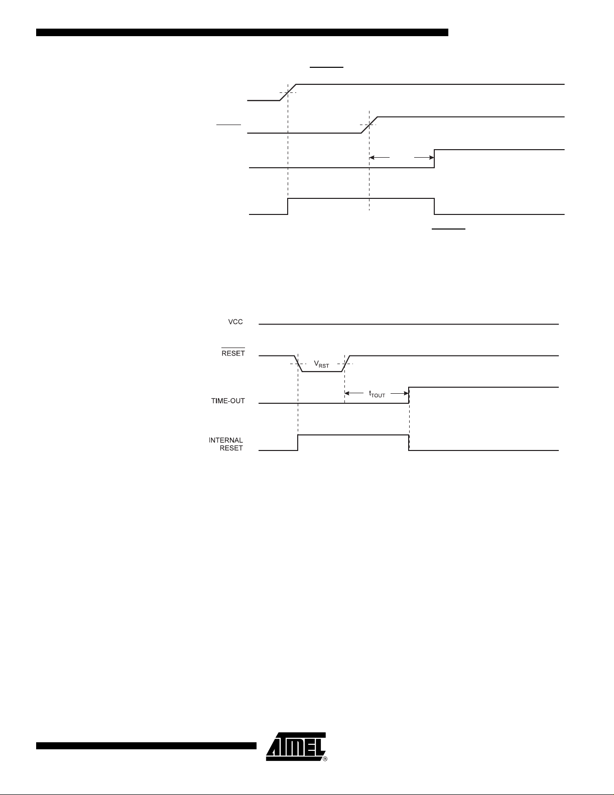
Figure 26. MCU Start-up, RESET Extended Externally
V
VCC
RESET
TIME-OUT
INTERNAL
RESET
POT
V
RST
t
TOUT
ATmega163(L)
External Reset An External Reset is generated by a low level on the RESET
pin. Reset pu lse s long er
than 500 ns will generate a Reset, even if the clock is not running. Shorter pulses are
not guaranteed to generate a Reset. When the applied signal reaches the Reset
Threshold Voltag e – V
Time-out Period t
TOUT
on its positive edge, the delay timer starts the MCU after the
RST
has expired.
Figure 27. External Reset During Operation
Brown-out Detection ATmega1 63 has an On -chip Brow n-out De tect ion (B OD) c ircuit for mo nitori ng t he V
level during the operation. The BOD circuit can be enabled/disabled by the fuse
BODEN. When the BOD is enabled (BODEN programmed), and V
decreases to a
CC
value below the t rigger l evel, the Bro wn-ou t Reset is i mmedia tely activa ted. Whe n V
increases above the trigger level, the B rown-out Reset is deactivated after a delay. T he
delay is defined by the user in the same way as the delay of POR signal, in Table 5. The
trigger level for the BOD can be selected by the fuse BODLEVEL to be 2.7V
(BODLEVEL unprogrammed), or 4.0V (BODLEVEL programmed). The trigger level has
a hysteresis of 50 mV to ensure spike free Brown-out Detection.
CC
CC
1142E–AVR–02/03
The BOD circuit will only detect a drop in V
if the voltage stays below the trigger level
CC
for longer than 9 µs for trigger level 4.0V, 21 µs for trigger level 2.7V (typical values).
27
Page 28
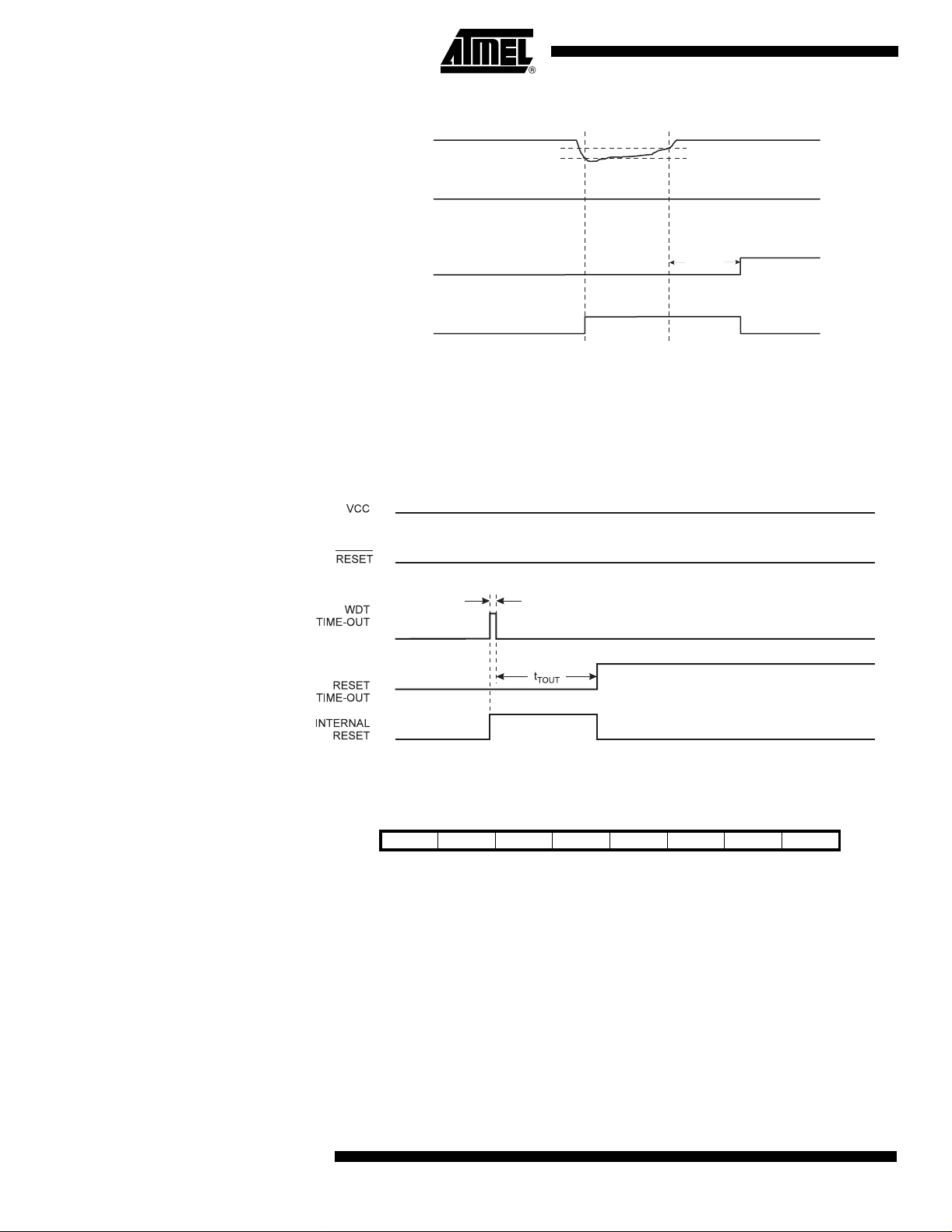
Figure 28. Brown-out Reset During Operation
= V
V
BOT+
t
TOUT
- 25 mV
BOT
VCC
RESET
TIME-OUT
INTERNAL
RESET
The hysteresis on V
BOT
: V
BOT+
= V
V
BOT-
+ 25 mV, V
BOT
BOT-
Watchdog Reset When the Watchdog times out, it will generate a short reset pulse of 1 XTAL cycle dura-
tion. On the falling edge of this pulse, the delay timer starts counting the Time-out Period
t
. Refer to page 60 for details on operation of the Watchdog Timer.
TOUT
Figure 29. Watchdog Reset During Operation
MCU Status Register – MCUSR
1 CK Cycle
The MCU Stat us Register p rovid es informati on on which reset source ca used an M CU
Reset.
Bit 76543210
$34 ($54) – – – – WDRF BORF EXTRF PORF MCUSR
Read/Write R R R R R/W R/W R/W R/W
Initial Value 0 0 0 0 See Bit Description
• Bits 7..4 – Res: Reserved Bits
These bits are reserved bits in the ATmega163 and always read as zero.
• Bit 3 – WDRF: Watchdog Reset Flag
This bit is set if a Watchdog Rese t occurs. The bit is reset by a Power-on Re set, or by
writing a logic zero to the Flag.
28
ATmega163(L)
1142E–AVR–02/03
Page 29

ATmega163(L)
• Bit 2 – BORF: Brown-out Reset Flag
This bit is set if a Brow n-ou t Reset occ urs. The bi t is reset by a P ower-on R eset, or by
writing a logic zero to the Flag.
• Bit 1 – EXTRF: Externa l Reset Flag
This bit is set if an External Reset occurs. The bit is reset by a Power-on Res et, or by
writing a logic zero to the flag.
• Bit 0 – PORF: Power-on Reset Flag
This bit is set if a P ower-on Res et occ urs. The bit is reset only by writing a logic zero to
the flag.
To make us e of the Re set Flags t o identify a res et co ndition, the u ser shou ld read an d
then reset the MCUSR as early as possible in the program. If the register is cleared
before another reset occurs, the source of the reset can be found by examining the
Reset Flags.
Internal Voltage Reference ATmega163 features an internal bandgap reference with a nominal voltage of 1.22V.
This re fe renc e is u sed fo r Br own -o ut D ete cti on, an d it ca n be u sed a s an i npu t to th e
Analog Co mparato r and AD C. The 2. 56V ref erence t o the ADC is also ge nera ted from
the internal bandgap reference.
Voltage Reference Enable Signals and St art-up Time
Interrupt H andling The ATmega163 has t wo 8-bit Interrupt Mask Control Registers: GIMSK – General
To save power, the reference is not always turned on. The reference is on during the following situations:
1. When the BOD is enabled (by programming the BODEN Fuse)
2. When the bandgap reference is connected to the Analog Comparator (by setting
the ACBG bit in ACSR) .
3. When the ADC is enabled.
Thus, when the BOD is not enabled, after setting the AC BG bit, the user mu st always
allow the re ferenc e to start up bef ore the out put f rom the Analo g Com par ator is used.
The bandgap reference us es typically 10 µA , and to reduce p ower consum ption in
Power-down mode, the user can avoid the three conditions above to ensure that the reference is turned off before entering Power-down mode.
Interrupt Mask Register and TIMSK – Timer/Counter Interrupt Mask Register.
When an interrupt occurs, the Global Interrupt Enable I-bit is cleared (zero) and all inter-
rupts are disabled. The user software must set (one) the I-bit to enable neste d
interrupts. The I-bit is set (one) when a Return from Interrupt instruction – RETI – is
executed.
When the Program Counter is vectored to the actual Interrupt Vector in order to execute
the interrupt handling routine, hardware clears the corresponding flag that generated the
interrupt. Some of the interrupt flags can also be cleared by writing a logic one to the flag
bit position(s) to be cleared.
1142E–AVR–02/03
If an interrupt condition occurs when the corresponding interrupt enable bit is cleared
(zero), the Interrupt Flag will be set and remembered until the interrupt is enabled, or the
flag is cleared by software.
29
Page 30

If one or more in terrupt cond itions oc cur when the Global Interru pt En able bit is cle ared
(zero), t he co rre spond ing in terru pt fl ag(s) will be se t an d rem ember ed until the G loba l
Interrupt Enable bit is set (one), and will be executed by order of priority.
Note that external level interrupt does not have a flag, and will only be rem embered for
as long as the interrupt condition is present.
Note that the Status Register is not automatically stored wh en entering an in terrupt routine and restored when returning from an interrupt routine. This must be handled by
software.
Interrupt Response Time The interrupt execution response for all the enabled AVR interrupts is four clock cycles
minimum. After four clock cycles the Program Vector address for the actual interrupt
handling routine is executed . During this four clock cycle period, the Program Co unter
(13 bits) is pushed onto the Stack. The vector is normally a jump to the interrupt routine,
and this jump takes three clock cycl e s. If an interrupt occurs during ex ec u ti o n of a multicycle instruction, this instruction is completed before the interrupt is served. If an interrupt occurs when the MCU is in sleep mode, the interrupt execution response time is
increased by four clock cycl es .
A return from an interrupt handling routine takes four clock cycles. During these four
clock cycles, the Program Counter (two bytes) is popped back from the Stack, the Stack
Pointer is incremen ted by two, an d the I Flag in SR EG is set. When
AVR
exits from an
interrupt, it will always return to the main program and execute one more instruction
before any pending interrupt is served.
The General Interrupt Mask Register – GIMSK
Bit 7 6 5 4 3 2 1 0
$3B ($5B) INT1 INT0 – – – – – – GIMSK
Read/Write R/W R/W R R R R R R
Initial Value 0 0 x 0 0 0 0 0
• Bit 7 – INT1: External Interrupt Request 1 Enable
When the IN T1 bit is set (one ) and the I-bi t in the Status Register (S REG) is s et (one),
the external pin interrupt is activated. The Interrupt Sense Control1 bits 1/0 (ISC11 and
ISC10) in the MCU general Control Register (MCUCR) define whether th e external
interrupt is activated on rising and/or falling edge of the INT1 pin or level sensed. Activity
on the p in wi ll caus e an interru pt re ques t ev en if IN T1 is con figure d a s an ou tpu t. Th e
corresponding interrupt of External Interrupt Reques t 1 is executed f rom program memory address $004. See also “External Interrupts”.
• Bit 6 – INT0: External Interrupt Request 0 Enable
When the IN T0 bit is set (one ) and the I-bi t in the Status Register (S REG) is s et (one),
the external pin interrupt is activated. The Interrupt Sense Control0 bits 1/0 (ISC01 and
ISC00) in the MCU General Control Register (MCUCR) define whether the external
interrupt is activated on rising or fall ing edg e of the INT0 pin or level se nsed. Activity on
the pin will cause an interrupt request even if INT0 is configured as an output. The corresponding interrupt of External Interrupt Request 0 is executed from Program Memory
address $002. See also “External Interrupts.”
30
• Bits 5 – Res: Reserved Bits
This bit is reserved in the ATmega163 and the read value is undefined.
ATmega163(L)
1142E–AVR–02/03
Page 31

The Genera l Int errupt Flag Register – GIFR
ATmega163(L)
• Bits 4..0 – Res: Reserved Bits
These bits are reserved bits in the ATmega163 and always read as zero.
Bit 7 6 5 4 3 2 1 0
$3A ($5A) INTF1 INTF0 – – – – – – GIFR
Read/Write R/W R/W R R R R R R
Initial Value 0 0 0 0 0 0 0 0
• B i t 7 – IN TF1: External In te rru pt Fl ag1
When an edge on the INT1 pin triggers an interrupt request, the corres pnding Int errupt
Flag, INTF1, becomes set (one). If the I-bit in SREG and the corresponding Interrupt
Enable bit, INT1 in GIMSK are set (one), th e MC U will jump t o the In terrupt Vecto r. The
Flag is cleared when the interrupt routine is executed. Alternatively, the Flag can be
cleare d by w ri ting a log ical one t o i t. Th is F lag is a lw ays clea red w he n IN T1 is conf igured as a level interrupt.
• B i t 6 – IN TF0: External In te rru pt Fl ag0
When an event on the INT0 pin triggers an interrupt request, the corresponding Interrupt
Flag, INTF0 becomes set (one). If the I-bit in SREG and the corresponding Interrupt
Enable bit, INT0 in GIMSK are set (one), th e MC U will jump t o the In terrupt Vecto r. The
Flag is cleared when the interrupt routine is executed. Alternatively, the Flag can be
cleare d by w ri ting a log ical one t o i t. Th is F lag is a lw ays clea red w he n IN T0 is conf igured as a level interrupt.
The Timer/Counter Interrupt Mask Register – TIMSK
• Bits 5..0 – Res: Reserved Bits
These bits are reserved bits in the ATmega163 and always read as zero.
Bit 7 6 5 4 3 2 1 0
$39 ($59) OCIE2 TOIE2 TICIE1 OCIE1A OCIE1B TOIE1 – TOIE0 TIMSK
Read/Write R/W R/W R/W R/W R/W R/W R R/W
Initial Value 0 0 0 0 0 0 0 0
• Bit 7 – OCIE2: Timer/Counter2 Outp ut Comp are Ma tch Interru pt Enable
When the OCIE2 bit is set (one) and the I-bit in the Status Register is set (one), the
Timer/Counter2 Compare Match Interrupt is enabled. The corresponding interrupt (at
vector $006 ) is e xecute d if a Com pare Ma tch in Timer/Co unte r2 oc curs, i.e ., when the
OCF2 bit is set in the Timer/Counter Interrupt Flag Register – TIFR.
• Bit 6 – TOIE2: Timer/ Counter2 Overflow Interrupt Enable
When the TOIE2 bit is set (one) and the I-bit in the Status Register is set (one), the
Timer/Counter2 Overflow Interrupt is enabled. The corresponding interrupt (at vector
$008) is executed if an overflow in Timer/Counter2 occurs, i.e., when the TOV2 bit is set
in the Timer/Counter Interrupt Flag Register – TIFR.
• Bit 5 – TICIE1: Timer/Counter1 Input Capture Interrupt Enable
1142E–AVR–02/03
When the TICIE1 bit is set (one) and the I-bit in the Status Register is set (one), the
Timer/C ount er1 In pu t Capt ure Ev en t Inter rup t is en ab led. T he co rre spond ing int erru pt
31
Page 32

(at vector $00A) is executed if a capture triggering event occurs on PD6 (ICP), i.e., when
the ICF1 bit is set in the Timer/Counter Interrupt Flag Register – TIFR.
• Bit 4 – OCIE1A: Timer/Coun ter1 Ou tput Comp areA M atch Interru pt Enable
When the OC IE1A bit is s et (one ) and the I- bit in the Sta tus Registe r is set (one), the
Timer/Counter1 Compare A Match Interrupt is enabled. The correspondin g interrupt (at
vector $00C) is executed if a Compare A Match in Timer/Counter1 occurs, i.e., when the
OCF1A bit is set in the Timer/Counter Interrupt Flag Register – TIFR.
• Bit 3 – OCIE1B: Timer/Coun ter1 Ou tput Comp areB M atch Interru pt Enable
When the OC IE1B bit is s et (one ) and the I- bit in the Sta tus Registe r is set (one), the
Timer/Counter1 Compare B Match Interrupt is enabled. The correspondin g interrupt (at
vector $00E) is executed if a Compare B Match in Timer/Counter1 occurs, i.e., when the
OCF1B bit is set in the Timer/Counter Interrupt Flag Register – TIFR.
• Bit 2 – TOIE1: Timer/ Counter1 Overflow Interrupt Enable
When the TOIE1 bit is set (one) and the I-bit in the Status Register is set (one), the
Timer/Counter1 Overflow Interrupt is enabled. The corresponding interrupt (at vector
$010) is executed if an overflow in Timer/Counter1 occurs, i.e., when the TOV1 bit is set
in the Timer/Counter Interrupt Flag Register – TIFR.
• Bit 1 – Res: Reserved Bit
This bit is a reserved bit in the ATmega163 and always reads as zero.
The Timer/Counter Interrupt Flag Register – TIFR
• Bit 0 – TOIE0: Timer/ Counter0 Overflow Interrupt Enable
When the TOIE0 bit is set (one) and the I-bit in the Status Register is set (one), the
Timer/Counter0 Overflow Interrupt is enabled. The corresponding interrupt (at vector
$012) is executed if an overflow in Timer/Counter0 occurs, i.e., when the TOV0 bit is set
in the Timer/Counter Interrupt Flag Register – TIFR.
Bit 7 6 5 4 3 2 1 0
$38 ($58) OCF2 TOV2 ICF1 OCF1A OCF1B TOV1 – TOV0 TIFR
Read/Write R/W R/W R/W R/W R/W R/W R R/W
Initial Value 0 0 0 0 0 0 x 0
• Bit 7 – OCF2: Output Compare Flag2
The OCF2 bit is set (one) when a Compare M atch occurs between the Tim er/Counter2
and the data in OCR2 – Output Compare Register2. OCF2 is cleared by hardware when
executing the corresponding Interrupt Handling Vector. Alternatively, OCF2 is cleared
by writing a lo gic one to th e flag. When the I-b it in SREG , and OCI E2 (Tim er/Counte r2
Compare Match Interrupt Enable), and the OCF2 are set (one), the Timer/Counter2
Comp are Ma t ch In terrupt i s execute d.
• Bit 6 – TOV2: Timer/Counter2 Overflow Flag
The TOV2 bit is set (one) when an overflow occurs in Timer/Counter2. TOV2 is cleared
by hardware when executing the corresponding inteRrupt Handling Vector. Alternatively, TOV2 is cleared by writing a logic one to the flag. When the SREG I-bit, and
TOIE2 (Timer/Counter2 Overflow Interrupt Enable), and TOV2 are set (one), the
32
ATmega163(L)
1142E–AVR–02/03
Page 33

ATmega163(L)
Timer/Counter2 Overflow Interrupt is e xecuted. In up/dow n PWM mode, th is bit is set
when Timer/Counter2 changes counting direction at $00.
• B i t 5 – ICF1 : Input Captu re Fl a g1
The ICF1 bit is set (one) to Flag an Input Capture Event, indicating that the
Timer/Counter1 value has been transferred to the Input Capture Register – ICR1. ICF1
is cleared by hardware when executing the corresponding Interrupt Handling Vector.
Alternatively, ICF1 is cleared by writing a logic one to the flag.
• Bit 4 – OCF1A: Output Compare Flag 1A
The OCF1A bit is set (one) when a Compare Match occurs between the Timer/Counter1
and the data in OCR1A – Out put Com pare Register 1A. OCF1A is cleared by ha rdware
when executing the corresponding Interrupt Handling Vector. Alternatively, OCF1A is
cleared by writing a logic one to the flag. When the I-bit in S REG, and O CIE1A
(Timer/Counter1 Compare Match Interrupt A Enable), and the OCF1A are set (one), the
Timer/Counter1A Compare Match Interrupt is executed.
• Bit 3 – OCF1B: Output Compare Flag 1B
The OCF1B bit is set (one) when a Compare Match occurs between the Timer/Counter1
and the data in OCR1B – Out put Com pare Register 1B. OCF1B is cleared by ha rdware
when executing the corresponding Interrupt Handling Vector. Alternatively, OCF1B is
cleared by writing a logic one to the flag. When the I-bit in S REG, and O CIE1B
(Timer/Counter1 Compare Match Interrupt B Enable), and the OCF1B are set (one), the
Timer/Counter1B Compare Match Interrupt is executed.
• Bit 2 – TOV1: Timer/Counter1 Overflow Flag
The TOV1 is set (one) when an overflow occurs i n T imer/Cou nter1. TOV 1 is c leared by
hardware when executing the corresponding Interrupt Handling Vector. Alternatively,
TOV1 is cl eared by writ ing a logi c on e to the flag. W hen the I-bit in SREG , and TOIE 1
(Timer/Counter1 Overflow Interrupt Enable), and TOV1 are set (one), the
Timer/Counter1 Overflow Interrupt is e xecuted. In up/dow n PWM mode, th is bit is set
when Timer/Counter1 changes counting direction at $0000.
• Bit 1 – Res: Reserved Bit
This bit is a reserved bit in the ATmega163 and the read value is undefined.
• Bit 0 – TOV0: Timer/Counter0 Overflow Flag
The bit TOV0 is set (one) when an overflow occurs in Timer/Counter0. TOV0 is cleared
by hardware when executing the corresponding Interrupt Handl ing Vector. Alternatively,
TOV0 is cleared by writing a logic one to the flag. When the SREG I-bit, and TOIE0
(Timer/Counter0 Overflow Interrupt Enable), and TOV0 are set (one), the
Timer/Counter0 Overflow interrupt is executed.
External Int errupts The external interrupts are triggered by the INT0 and INT1 pins. Observe that, if
enabled, the interrupts will trigger even if the INT0/INT 1 pin s are c on figured as out puts.
This fe ature p rovi des a way of g enera ting a soft ware interru pt. T he ex terna l inte rru pts
can be triggere d by a fal ling or rising edg e or a low lev el. This is set up as indi cated i n
the specification for the MCU Control Register – MCUCR. When the external interrupt is
enabled and is configured as level triggered, the interrupt will trigger as long as the pin i s
held low.
1142E–AVR–02/03
33
Page 34

MCU Control Register – MCUCR
The MCU Control Register contains control bits for general MCU functions.
Bit 76543210
$35 ($55) – SE SM1 SM0 ISC11 ISC10 ISC01 ISC00 MCUCR
Read/Write R R/W R/W R/W R/W R/W R/W R/W
Initial Value00000000
• Bit 7 – Res: Reserved Bit
This bit is a reserved bit in the ATmega163 and always reads as zero.
• Bit 6 – SE: Sleep Enable
The SE bit must be set (one) to make the MCU enter the sleep mode when the SLEEP
instruction is executed. To avoid the MCU en tering the sleep mod e unless it is the programmers purpose, it is recommended to set the Sleep Enable SE bit just before the
execution of the SLEEP instruction.
• Bit s 5, 4 – SM1/SM0: Sleep Mode Se lect Bits 1 and 0
These bits select between the three available sleep modes as shown in Table 7.
Table 7. Sleep Mode Select
SM1 SM0 Sleep Mode
00Idle
0 1 ADC Noise Reduction
1 0 Power-down
11Power-save
• Bits 3, 2 – ISC11, ISC10: Interrupt Sense Control 1 Bit 1 and Bit 0
The External Interrupt 1 is activated by the external pin INT1 if the SREG I-Flag and the
corresponding interrupt mask in the GIMSK are set. The level and edges on the external
INT1 pin that activate t he interrupt are defined in Table 8. Th e value on th e INT1 pin is
sampled before detecting edg es. If edge or togg le interrupt is selected, pulses that last
longer th an one cl ock p eriod w ill gener ate an inte rrupt. Sh orter p ulses are no t guaranteed to generate an interrupt. If low level interrupt is selected, the low level must be held
until the completion of the currently executing instruction to generate an interrupt.
Table 8. Interrupt 1 Sense Control
ISC11 ISC10 Description
0 0 The low level of INT1 generates an interrupt request.
0 1 Any logical change on INT1 generat es an interrupt request.
1 0 The falling edge of INT1 generates an i nterrupt request.
1 1 The rising edge of INT1 generates an interrupt request.
34
ATmega163(L)
1142E–AVR–02/03
Page 35

ATmega163(L)
• Bit 1, 0 – ISC01, ISC00: Interrupt Sense Control 0 Bit 1 and Bit 0
The External Interrupt 0 is activated by the external pin INT0 if the SREG I-Flag and the
corresponding interrupt mask are set. The level and edges on the external INT0 pin that
activate the interrupt are defined in Table 9. The value on t he INT0 pin is sample d
before detecting edges. If edge or toggle interrupt is selected, pulses that last longer
than o ne c lock peri od wi ll g ener ate an i nterru pt. Sho rter pu lses are no t g uar ante ed to
generate an interrupt. If low level interrupt is selected, th e low level must be h eld until
the completion of the currently executing instruction to generate an interrupt.
Table 9. Interrupt 0 Sense Control
ISC01 ISC00 Description
0 0 The low level of INT0 generates an interrupt request.
0 1 Any logical change on INT0 generat es an interrupt request.
1 0 The falling edge of INT0 generates an i nterrupt request.
1 1 The rising edge of INT0 generates an interrupt request.
Sleep Modes To enter any of the four sleep modes, the SE bit in MCUCR must be set (one) and a
SLEEP instruction must be executed. Th e SM1 and SM0 bits in the MCUCR Regis ter
select which sleep mode (Idle, ADC Noise Reduct ion, Power-down, or Power-save) will
be activated by the SLEEP instruction. See Table 7 for a summary. If an enabled interrupt occurs while the MCU is in a sleep mode, the MCU wakes up. The MCU is then
halted for fo ur cycle s, execute s the inte rrupt routine, an d res umes e xecution fro m th e
instruction following SLEEP. The contents of the Register File, SRAM, and I/O memory
are unaltered when the device wakes up from sleep. If a Reset occurs during sleep
mode, the MCU wakes up and executes from the Reset Vector.
Idle Mode When the SM1/SM0 bits are set to 00, the SLEEP instruction makes the MCU enter Idle
mode, stopping t he CPU but allowing SPI, UART, Analog Comp arator, A DC, Two-wi re
Serial Interface, Timer/Count ers, Watchdog , and the interrupt s ystem to continue operating (if enabl ed). Th is ena bles t he M CU t o wake u p fro m exter nal t rigge red in terrupt s
as well as internal ones like the Timer Overflow and UART Receive Complete interrupts.
If wake-up from the Analog Comparator interrupt is not required, the Analog Comparator
can be powered down by setting the ACD bit in the Analog Comparator Control and Status Reg ist er – A CSR . T his w ill redu ce po we r cons ump tio n in I dle Mo de. I f the A DC i s
enabled, a conversion starts automatically when this mode is entered.
ADC Noise Reduction Mode When the SM1/SM0 bits are set to 01, the SLEEP instruction makes the MCU enter
ADC Noise Reduction mode, stopping the CPU but allowing the ADC, the external interrupts, the Two- wire Serial Int erface addre ss wat ch, Timer/ Counter2 an d the W atchdo g
to continue operating (if enabled). This improves the noise environment for the ADC,
enabling higher resolution measurements. If the ADC is enabled, a conversion starts
automatically when this mode is entered. Apart from the ADC Conversion Complete
interrupt, only an External Reset, a Watchd og Reset (if enabled), a Brow n-out Reset, a
Two-wire Serial Interface address match interrupt, or an external level interrupt can
wake up the MCU from ADC Noise Reduction Mode. A Timer/Counter2 Output Compare or overflow event will wake up the MCU, but will not generate an interrupt unless
Timer/Counter2 is clocked asynchronously.
In future devices this is subject to change. It is recommended for future code compatibility to disable Timer/Counter2 interrupts during ADC Noise Reduction mode if the
Timer/Counter2 is clocked synchronously.
1142E–AVR–02/03
35
Page 36

Power-do wn M ode When the SM1/SM0 bits are 10, the SLEEP instruction makes the MCU enter Po wer-
down mode. In this mode, the external Oscillator is stopped, while the external interrupts, the Two-wire Serial Interface address match, and the Watchdog continue
operating (if enabled). Only an External Reset, a Watchdog Reset, a Brown-out Reset, a
Two-wire Serial Interface address match interrupt, or an external level interrupt can
wake up the MCU.
Note that if a lev el triggered inte rrupt is used f or wake-u p from Power-do wn mod e, the
change d leve l mu st be held fo r some time to wa ke u p the M CU . This make s the M C U
less sensitive to noise. The changed level is sam pled twice by the Watc hdog Oscillator
clock, and if the input has the required level during this time, the MCU will w ak e up. The
period of the Watchdog Oscillator i s 1 µs (nominal) at 5. 0V and 25°C. T he frequency of
the Watchdog Oscil lator is v oltage de pendent as shown in the Ele ctrical Characteristics
section.
When wa king up from P ower-d own m ode, t here is a delay f rom the wak e-up co nd ition
occurs until the wake-up becomes effective. This allows the clock to restart and become
stable after having been stopped. The wake-up period is defined by the same CKSEL
Fuses that define the Reset Time-out period, as seen in Table 5 on page 25.
Power-save Mode When the SM1 /SM0 bits are 11, the SLEEP instruction forces the MCU into the Power-
save mode. This mode is identical to Power-down, with one exception:
If Timer/Counter 2 is clocked asynchrono usly, i.e., the AS2 bit in ASSR is set,
Timer/Counter2 will run durin g sleep. Th e device c an wake up from either T imer Ov erflow or Output Compare event from Timer/Counter2 if the corresponding
Timer/Co unt er2 int errupt e nab le bit s are s et in TI MSK , and t he g lobal interr upt e nable
bit in SREG i s se t .
If the asynchronous timer is NOT clocked asynchronously, Power-down mode is recommended instead of Power-save mode because the contents of the registers in the
asynchronous timer should be considered undefined after wake-up in Power-save mode
if AS2 is 0.
36
ATmega163(L)
1142E–AVR–02/03
Page 37
ATmega163(L)
Calibrated Internal RC Oscillator
Oscillator Calibration Register – OSCCAL
The calibrated internal Oscillator provides a fixe d 1 MHz (nominal) clock at 5V and
25°C. This clock may be used as the system clock. See the section “Clock Options” on
page 5 for informat ion on how to select this c lock as th e system c lock. This Oscillator
can be calibrated by writing the calibration byte to the OSCCAL Register. When this
Oscillator is used a s the chip clock, the Watch dog Os cillator will still be used f or the
Watchdog Timer and for the Reset Time-out. At 5V and 25
o
C, the pre-programmed calibration byte gives a frequency within ± 1% of the nominal frequency. For details on how
to use the pre-programmed calibration value, see “Calibration Byte” on page 144.
Bit 76543210
$31 ($51) CAL7 CAL6 CAL5 CAL4 CAL3 CAL2 CAL1 CAL0
Read/Write R/W R/W R/W R/W R/W R/W R/W R/W
Initial Value00000000
• Bits 7..0 – CAL7..0: Oscillator Calibration Value
Writing the calibration byte to this address will trim the internal Oscillator to remove process variations from the Oscillator frequency. When OSCCAL is zero, the lowest
available frequen cy is c hosen. W riting non-ze ro values to this regis ter will increa se the
frequen cy of t he i nternal Os cillat or. Wri ting $F F t o the re gis ter give s the high est a vai lable frequency.
The calibrated Oscillator is used to time EEPROM and Flash access. If EEPROM or
Flash is written, do not calibrate to more than 10% above the nominal frequency. Otherwise, the EEPROM or Flash write operation may fail. Note that the Oscillator is intended
for calibration to 1.0MHz, thus tuning to other values is not guaranteed.
Special Function I/O Register – SFIOR
Table 10. Internal RC Oscillator Frequency Range.
OSCCAL Value Min Frequency (MHz) Max Frequency (MHz)
$00 0.5 1.0
$7F 0.7 1.5
$FF 1.0 2.0
Bit 7 6 5 4 3 2 1 0
$30 ($50) – – – – ACME PUD PSR2 PSR10 SFIOR
Read/Write R R R R R/W R/W R/W R/W
Initi al Valu e 0 0 0 0 0 0 0 0
• Bit 7..4 – Re s: Res erved Bits
These bits are reserved bits in the ATmega163 and always read as zero.
• Bit 3 – ACME: Analog Comparator Multiplexer Enable
When this bit is set (one) and the ADC is switched off (ADEN in ADCSR is zero), the
ADC multiplexer selects the negative input to the Analog Comparator. When this bit is
cleared (zero), AIN1 is applied to the negative input of the Analog Comparator. For a
detailed description of this bit, see “Analog Comparator Multiplexed Input” on page 104.
1142E–AVR–02/03
37
Page 38

• Bit 2 – PUD: Pull-up Disable
When this bit is set (one), all pull-ups on all ports are disabled. If the bit is cleared (zero),
the pull-ups can be in dividually enabled as described in th e chapt er “I/O Ports” on pa ge
115.
• Bit 1 – PSR2: Prescaler Reset Timer/Counter2
When this bit is set (one) the Timer/Counter2 Prescaler will be reset. The bit will be
cleared by hardware after the operation is performed. Writing a zero to this bit will have
no effect. This bit will always be read as zero if Timer/Counter2 is clocked by the internal
CPU clock . If this bit is written wh en Timer/C ounter2 is ope rating in async hronous
mode. The bit will remain one until the prescaler has been reset. See “Asynchronous
Operation of Timer/Counter2” on page 58 for a detailed description of asynchronous
operation.
• Bit 0 – PSR10: Prescaler Reset Timer/Counter1 and Timer/Counter0
When this bi t is set (one) the Time r/Counter1 a nd Timer/Counter0 Presca ler will be
reset. The bit will be c leared by hardware a fter the oper ation is per formed. Writing a
zero to this bit will have no effect. Note that Timer/Count er1 and Timer/Coun ter0 share
the same prescaler and a reset of this prescaler will affect both timers. This bit will
always be read as zero.
38
ATmega163(L)
1142E–AVR–02/03
Page 39

ATmega163(L)
Timer/Counters The ATmega163 pro vides t hree ge neral purpos e Tim er/Coun ters – t wo 8-b it T/ Cs and
one 16-bit T/C. Timer/Counter2 can optionally be asynchronously clocked from an external Oscillator. This O scillator is optimized for us e with a 32.768 kHz watc h crystal,
enabling u se of Timer/Co unter2 as a Real Time Cloc k (RTC). Timer/ Counter0 an d
Timer/Counter1 have individual prescaling selection from the same 10-bit prescaler.
Timer/Counter2 has its own prescaler. Both these prescalers can be reset by setting the
corresponding control bits in the Special Functions I/O Register (SFIOR). These
Timer/C ount ers ca n e ither be us ed a s a tim er wi th a n inte rnal clock t ime- ba se or as a
counter with an external pin connection which triggers the counting.
Timer/Counter Prescalers
Figure 30. Prescaler for Timer/Counter0 and Timer/Counter1
Clear
PSR10
TCK1 TCK0
For Timer/Counter0 and Timer/Counter1, the four different prescaled selections are:
CK/8, CK/64, CK/256, and CK/1024, where CK is the Oscillator clock. For the two
Timer/Counter0 and Timer/Counter1, CK, external source, and stop can also be
selected as clock sources. Setting the PSR10 bit in SFIOR resets the prescaler. This
allows the user to operate with a predictable prescaler. Note that Timer/Counter1 and
Timer/Counter0 share the same prescaler and a Prescaler Reset will affect both
Timer/Counters.
1142E–AVR–02/03
39
Page 40

Figure 31. Prescaler for Timer/Counter2
CK
TOSC1
AS2
PSR2
CS20
CS21
CS22
PCK2
Clear
TIMER/COUNTER2 CLOCK SOURCE
10-BIT T/C PRESCALER
PCK2/8
0
TCK2
PCK2/32
PCK2/64
PCK2/256
PCK2/128
PCK2/1024
The clock source for Time r/Counter2 is named P CK2. PC K2 is by default connec ted to
the main system clock CK. By setting the AS2 bit in ASSR, Timer/Counter2 is asynchronously clocked from the PC6(TOSC1) pin. This enables use of Timer/Counter2 as a
Real Time Clock (RTC). When AS2 is set, pins PC6(TOSC1) and PC7(TOSC2) are disconnected from Port C. A crystal can then be connected between the PC6(TO S C1) and
PC7(TOSC2) pins to serve as an independent clock source for Timer/Counter2. The
Oscillator is optimized for use with a 32.768 kHz crystal. Applying an external clock
source to TOSC1 is not recom mended. S etting the PSR2 bi t in SFIOR resets the prescaler. This allows the user to operate with a predictable prescaler.
8-bit Timer/Counter0 Figure 32 shows the block diagram for Timer/Counter0.
The 8-bit Timer/Counter0 can select clock source from CK, prescaled CK, or an external
pin. In addition it can be stopped as described in “Timer/Counter0 Control Register –
TCCR0” on page 41. The overflow Status Flag is found in “The Timer/Counter Interrupt
Flag Register – TIFR” on page 32. Control signals are found in the Timer/Counter0 Control Register – TCCR0. The interrupt enable/disable settings for Timer/Counter0 are
found in “The Timer/Counter Interrupt Mask Register – TIMSK” on page 31.
When Timer/Counter0 is externally clo cked, the exte rnal signa l is synchro nized with the
Oscillator frequency of the CPU. To assure proper sampling of the external clock, the
minimum time between two ex ternal clock transitions must be at least one i ntern al CPU
clock period. The external clock signal is sampled on the rising edge of the internal CPU
clock.
The 8-bit Timer/Counter0 features both a high resolution and a high accuracy usage
with the lower prescaling opportunities. Similarly, the high prescaling opportunities make
the Timer/Counter0 useful for lower speed functions or exac t timing functions with infrequent actions.
40
ATmega163(L)
1142E–AVR–02/03
Page 41

Figure 32. Timer/Counter0 Block Diagram
T/C0 OVER-
FLOW IRQ
OCIE1A
TA BUS
8-BIT DA
OCIE1B
TICIE1
TOIE2
OCIE2
TIMER INT. MASK
REGISTER (TIMSK)
TOIE1
TOIE0
TIMER INT. FLAG
REGISTER (TIFR)
TOV2
OCF2
ICF1
OCF1B
OCF1A
TOV1
TOV0
ATmega163(L)
T/C0 CONTROL
REGISTER (TCCR0)
CS00
CS01
CS02
Timer/Counter0 Control Register – TCCR0
07
TIMER/COUNTER0
(TCNT0)
Bit 76543210
$33 ($53) –––––CS02CS01CS00TCCR0
Read/Write RRRRRR/WR/WR/W
Initial Value00000000
T/C CLK SOURCE
CONTROL
LOGIC
• Bits 7..3 – Res: Reserved Bits
These bits are reserved bits in the ATmega163 and always read as zero.
• Bits 2..0 – CS02, CS01, CS00: Clock Select0, Bit 2, 1, and 0
The Clock Select0 bits 2,1, and 0 define the prescaling source of Timer0.
Table 11. Clock0 Prescale Select
CS02 CS01 CS00 Description
0 0 0 Stop, Timer/Counter0 is stopped.
001CK
CK
1142E–AVR–02/03
010CK/8
011CK/64
100CK/256
101CK/1024
1 1 0 External Pin T0, falli ng edge
1 1 1 External Pin T0, rising edge
The Stop condition provides a Timer Enable/Disable function. The prescaled CK modes
are scale d direct ly from the CK Os cillato r clock . If th e externa l pin m ode s are used f or
Timer/Count er0, tra nsitions on PB0 /(T0) will c lock the counte r even if th e pin is con figured as an output. This feature can give the user SW control of the counting.
41
Page 42

Timer/Counter 0 – TCNT0
Bit 76543210
$34 ($54) MSB LSB TCNT0
Read/Write R/W R/W R/W R/W R/W R/W R/W R/W
Initial Value00000000
The Timer/Counter0 is implement ed as an up-counter with read and write access. If t he
Timer/Counter0 is written a nd a clock s ource is prese nt, the Tim er/Count er0 cont inues
counting in the clock cycle following the write operation.
16-bit Timer/ Counter1 Figure 33 shows the block diagram for Timer/Counter1.
Figure 33. Timer/Counter1 Block Diagram
T/C1 OVER-
FLOW IRQ
TOIE1
OCIE1A
OCIE1B
TICIE1
TOIE2
TA BUS
8-BIT DA
OCIE2
TIMER INT. MASK
REGISTER (TIMSK)
15
T/C1 INPUT CAPTURE REGISTER (ICR1)
T/C1 COMPARE
TOIE0
8
7
MATCH A IRQ
TOV2
OCF2
TIMER INT. FLAG
REGISTER (TIFR)
ICF1
ICF1
OCF1B
OCF1B
T/C1 COMPARE
MATCH B IRQ
TOV0
OCF1A
TOV1
TOV1
OCF1A
CAPTURE
TRIGGER
T/C1 INPUT
CAPTURE IRQ
T/C1 CONTROL
REGISTER A (TCCR1A)
COM1B1
COM1A1
COM1A0
0
COM1B0
FOC1A
FOC1B
PWM11
PWM10
T/C1 CONTROL
REGISTER B (TCCR1B)
ICNC1
ICES1
CONTROL
LOGIC
CTC1
CS12
CS11
CS10
T1
CK
15
15
15
TIMER/COUNTER1 OUTPUT COMPARE REGISTER A
8
7
TIMER/COUNTER1 (TCNT1)
8
7
16 BIT COMPARATOR
8
7
T/C CLEAR
0
T/C CLOCK SOURCE
UP/DOWN
8
15
0
15
0
TIMER/COUNTER1 OUTPUT COMPARE REGISTER B
7
16 BIT COMPARATOR
8
7
0
0
The 16-bit Timer/Counter1 can select clock source from C K, prescale d CK , or an e xternal pin. In addition it can be stopped as described in section “Timer/Counter1 Control
Register B – TCCR1B” on page 45. The different Status Flags (Overflow, Compare
Match, and Capture Event) are found in the Timer/Counter Interrupt Flag Register –
TIFR. Control signals are found in the Timer/Counter1 Control Registers – TCCR1A and
TCCR1B. The interrupt enable/disable settings for Timer/Counter1 are found in the
Timer/Counter Interrupt Mask Register – TIMSK.
When Timer/Counter1 is externally clo cked, the exte rnal signa l is synchro nized with the
Oscillator frequency of the CPU. To assure proper sampling of the external clock, the
minimum time between two ex ternal clock transitions must be at least one i ntern al CPU
42
ATmega163(L)
1142E–AVR–02/03
Page 43

ATmega163(L)
clock period. The external clock signal is sampled on the rising edge of the internal CPU
clock.
The 16-b it Time r/Co unter1 fea tur es both a high resol ution an d a h igh a ccu racy u sag e
with the lower prescal ing opportunities. S imilarly, the high prescaling op portunities
makes the Timer/Counter1 useful for lower speed functions or exact timing functions
with infrequent actions.
The Timer/Counter1 supports two Output Compare functions using the Output Compare
Register 1 A and B (OCR1A and OCR1B) as the data sources to be compared to the
Timer/Counter1 contents. The Output Compare functions includes optional clearing of
the counter on Compare A Match, and actions on the Output Compare pins on both
compare matches.
Timer/Counter1 can also be used as an 8-, 9-, or 10-bit Pulse Width Modulator (PWM).
In this mode the coun ter and the O CR1 A/OCR1 B Regist ers serve as a dual g litch-free
stand-alo ne PW M with cente red pul ses. Altern ativ ely, the Timer/ Counte r1 can be co nfigured to operate at twice the s peed in PWM mo de, but without c entered pulses. Refer
to page 48 for a detailed description of this function.
The Input Capture function of Timer/Counter1 provides a capture of the Timer/Count er1
contents to the Input Capture Register – ICR1, triggered by an external event on the
Input Cap ture Pin – ICP. The actual cap ture event settings are defined by the
Timer/Counter1 Control Register – TCCR1B. In addition, the Analog Comparator can be
set to trigger the Input Capture. Refer to the section, “The Analog Comparator” on page
102, for details on this. The ICP pin logic is shown in Figure 34.
Figure 34. ICP Pin Schematic Diagram
If the noise canceler function is enabled, the actual trigger condition for the capture
event is monitored over four samples, and all four must be equal to activate the Capture
Flag.
1142E–AVR–02/03
43
Page 44
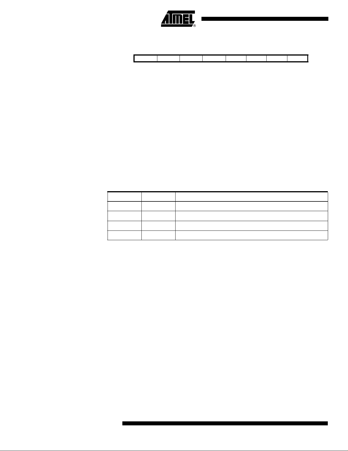
Timer/Counter1 Control Register A – TCCR1A
Bit 7 6 5 4 3210
$2F ($4F) COM1A1 CO M1A0 COM1B1 COM1B0 FOC1A FOC1B PWM11 PWM10 TCCR1A
Read/Write R/W R/W R/W R/W R/W R/W R/W R/W
Initi al Valu e 0 0 0 0 0 0 0 0
• Bits 7, 6 – COM1A1, COM1A0 : Compare Output Mode1A, Bits 1, and 0
The COM1A1 and COM 1A0 control bits determine any output pin action following a
Compare Match in Timer/Counter1. Any output pin actions affect pin OC1A – Output
Compare A. Th is is an alterna tive funct ion to an I/O Port, and th e correspondi ng direction control bit must be set (one) to control an output pin. The control configuration is
shown in Table 10.
• Bits 5, 4 – COM1B1, COM1B0 : Compare Output Mode1B, Bits 1, and 0
The COM1B1 and COM 1B0 control bits determine any output pin action following a
Compare Match in Timer/Counter1. Any output pin actions affect pin OC1B – Output
Compare B . This is an alter native fu nction t o an I/O port, and the corre spondin g direction control bit must be set (one) to control an output pin. The control configuration is
shown in Table 10.
Table 12. Compare 1 Mode Select
COM1X1 COM1X0 Description
0 0 Timer/Counter1 disconnected from output pin OC1X
0 1 Toggle the OC1X output line.
1 0 Clear the OC1X output line (to zero).
1 1 Set the OC1X output line (to one).
Note: 1. X = A or B.
(1)
In PWM mode, these bits have a different function. Refer to Table 14 for a detailed
description.
• Bit 3 – FOC1A: Force Output Compare1A
Writing a logical one to this bit, forces a change in the Com pare Match Out put pin PD5
according to the v alues already set in COM1A1 and CO M1A0. If the CO M1A1 and
COM1A0 bits are written in the same cycle as FOC1A, the new settings will not take
effect unt il nex t C ompar e M atc h or F orce d C omp are M at ch occ urs . Th e Fo rce O utp ut
Compare bit can be used to change the output pin without waiting for a Compare Match
in the Timer. The automatic action programmed in COM1A1 and COM1A0 happens as if
a Compare Match had occurred, but no interrupt is generated and it will not clear the
timer even if CTC1 in TCCR1B is set. The corresponding I/O pin must be set as an output pin for the FOC1A bit to have effect on the pin. The FOC1A bit will always be read as
zero. The setting of the FOC1A bit has no effect in PWM mode.
44
• Bit 2 – FOC1B: Force Output Compare1B
Writing a logical one to this bit, forces a change in the Com pare Match Out put pin PD4
according to the v alues already set in COM1B1 and CO M1B0. If the CO M1B1 and
COM1B0 bits are written in the same cycle as FOC1B, the new settings will not take
effect unt il nex t C ompar e M atc h or F orce d C omp are M at ch occ urs . Th e Fo rce O utp ut
Compare bit can be used to change the output pin without waiting for a Compare Match
ATmega163(L)
1142E–AVR–02/03
Page 45

ATmega163(L)
in the Timer. The automatic action programmed in COM1B1 and COM1B0 happens as if
a Comp are Mat ch ha d o ccu rred, bu t no i nte rrupt i s g ener ate d. Th e c orres po ndin g I /O
pin must be set as an output pin for the FOC1B bit to have effect on the pin. The FOC1B
bit will always be read as zero. The setting of the FOC1B bit has no effect in PWM
mode.
• Bits 1..0 – PWM11, PWM1 0: Pulse Width Mod ulator Select Bits
These bits select PWM operation of Timer/Counter1 as specified in Table 11. This mode
is described on page 48.
Table 13. PWM Mode Select
PWM11 PWM 10 Description
0 0 PWM operation of Timer/Counter1 is disabled
0 1 Timer/Counter1 is an 8-bit PWM
1 0 Timer/Counter1 is a 9-bit PWM
1 1 Timer/Counter1 is a 10-bit PWM
Timer/Counter1 Control Register B – TCCR1B
Bit 76543210
$2E ($4E) ICNC1 ICES1 – – CTC1 CS12 CS11 CS10 TCCR1B
Read/Write R/W R/W R R R/W R/W R/W R/W
Initial Value00000000
• Bit 7 – ICNC1: Input Capture1 Noise Canceler (4 CKs)
When the ICNC1 bit is cleared (zero), the Input Capt ure trigger noise canceler fun ction
is disabled. The Input Captu re is triggered at the first rising/falling edge sample d on t he
ICP – Input Capture Pin – as specified. When the ICNC1 bit is set (one), four successive
samples are measures on the ICP – Input Capture Pin, and all samples must be
high/low according to the Input Capture trigger specification in the ICES1 bit. The actual
sampling frequency is XTAL clock frequency .
• Bit 6 – ICES1: Input Capture1 Edge Select
While the ICES1 bit is cleared (zero), the Timer/Counter1 contents are transferred to the
Input Capture Register – ICR1 – on the falling edge of the Input Capture Pin – ICP.
While the ICES1 bit is set (one), the Timer/Counter1 contents are transferred to the
Input Capture Register – ICR1 – on the rising edge of the Input Capture Pin – ICP.
• Bits 5, 4 – Res: Reserved Bits
These bits are reserved bits in the ATmega163 and always read as zero.
1142E–AVR–02/03
• Bit 3 – CTC1: Clear Timer/Counter1 on Compare Match
When the CTC1 control bit is set (one), the Timer/Counter1 is Reset to $0000 in the
clock cycle after a Compare A Match. If the CTC1 control bit is cleared, Timer/Counter1
contin ues coun ti ng an d is un affe cted by a Co mpa re Matc h. W hen a p res cali ng o f 1 is
used, and the Compare A Register is set to C, the timer will count as follows if CTC1 is
set:
... | C-1 | C | 0 | 1 |...
45
Page 46

When the prescaler is set to divide by eight, the Timer will count like this:
... | C-1, C-1, C-1, C-1, C-1, C-1, C-1, C-1 | C, C, C, C, C, C, C, C | 0, 0, 0, 0, 0, 0, 0 , 0
|1,1,1,1,1,1,1,1|...
In PWM mode, this bit has a di fferent function. I f the CTC 1 bit is cleared in PWM mode,
the Timer/Counter1 acts as an up/down counter. If the CTC1 bit is set (one), the
Timer/Counter wraps when it reaches the TOP value. Refer to page 48 for a detailed
description.
• Bits 2..0 – CS12, CS11, CS10: Clock Select1, Bit 2, 1, and 0
The Clock Select1 bits 2, 1, and 0 define the prescaling source of Timer/Counter1.
Table 14. Clock 1 Prescale Select
CS12 CS11 CS10 Description
0 0 0 Stop, the Timer/Counter1 is stopped.
001CK
010CK/8
011CK/64
100CK/256
1 0 1 CK/1024
1 1 0 External Pin T1, falling edge
Timer/Counter1 – TCNT1H and TCN T1L
1 1 1 External Pin T1, rising edge
The Stop condition provides a Timer Enable/Disable function. The prescaled modes are
scaled directly fr om the CK Osc illator clock. If the ex ternal pin modes are u sed for
Timer/Count er1, tra nsitions on PB1 /(T1) will c lock the counte r even if th e pin is con figured as an output. This feature can give the user SW control of the counting.
Bit 151413121110 9 8
$2D ($4D) MSB TCNT1H
$2C ($4C) LSB TCNT1L
76543210
Read/Write R/W R/W R/W R/W R/W R/W R/W R/W
R/W R/W R/W R/W R/W R/W R/W R/W
Initial Value00000000
00000000
This 16-bit register contains the prescaled value of the 16-bit Timer/Counter1. To
ensure tha t both th e high and low byte s are read an d writ ten sim ultane ous ly when the
CPU accesses these registers, the access is performed using an 8-bit temporary register (TEMP). This temporary register is also used when accessing OCR1A , OCR1B, a nd
ICR1. If the main program and also interrupt routines perform access to registers using
TEMP, interrup ts mu st be disa bled du ring access from the m ain pro gram an d interrupt
routines.
46
ATmega163(L)
1142E–AVR–02/03
Page 47

ATmega163(L)
TCNT1 Tim er/ C ounter1 Write When th e CPU writes to the high byte TCNT1H, the written data is placed in the TEMP
Register. Next, when the CPU writes the low byte TCNT1L, this byte of data is combined
with the byte data in the TEMP Re gister, and all 16 b its are written to the T CNT1
Timer/Counter1 Register simultaneously. Consequently, the high byte TCNT1H must be
accessed first for a full 16-bit register write operation.
TCNT1 Tim er/ C ounter1 Read When the CPU reads the low byte TCNT1L, the data of the Low Byte TCNT1L is sent to
the CPU and the data of the High Byte TCNT1H is placed in the TEMP Register. When
the CPU reads the data in the High Byte TCNT1H, the CPU receives the data in the
TEMP Re gister. Conseq uent ly, the L ow By te TCNT 1L mu st be a ccesse d first fo r a full
16-bit register read operation.
The Timer/Counter1 is realized as an up or up/ down (in PWM mode) counter with read
and write access. If Timer/Counter1 is written to and a clock source is selected, the
Timer/Counter1 continues counting in the timer clock cycle after it is preset with the written value.
Timer/Counter1 Output Compare Register – OCR1AH and OCR1AL
Bit 151413121110 9 8
$2B ($4B) MSB OCR1AH
$2A ($4A) LSB OCR1AL
76543210
Read/Write R/W R/W R/W R/W R/W R/W R/W R/W
R/W R/W R/W R/W R/W R/W R/W R/W
Initial Value00000000
00000000
Timer/Counter1 Output Compare Register – OCR1BH and OCR1BL
Bit 151413121110 9 8
$29 ($49) MSB OCR1BH
$28 ($48) LSB OCR1BL
76543210
Read/Write R/W R/W R/W R/W R/W R/W R/W R/W
R/W R/W R/W R/W R/W R/W R/W R/W
Initial Value00000000
00000000
The Output Compare Registers are 16-bit read/write registers.
The Timer/Counter1 Output Compare Registers contain the data to be continuously
comp ared w ith Tim er/C ounter 1. Ac tions on com pare m atch es ar e spe cified in the
Timer/Counter1 Control and Status Register. A software write to the Timer/Counter
Register blocks compare matches in the next Timer/Counter clock cycle. This prevents
immediate interrupts when initializing the Timer/Counter.
A Compare Match will set the compare interrupt flag in the CPU clock cycle following the
compare event.
Since the Output Compare Registers – OCR1A and OCR1B – are 16-bit registers, a
temporary register TEM P is used wh en OCR1A /B are written to ensure that both by tes
are updated simultaneously. When the CPU writes the high byte, OCR1AH or OCR1BH,
the data is temporarily stored in the TEMP Register. When the CPU writes the Low Byte,
OCR1AL or OCR1BL, the TEMP Register is simultaneously written to OCR1AH or
OCR1BH. Consequently, the high byte OCR1AH or OCR1BH must be written first for a
full 16-bit register write operation.
1142E–AVR–02/03
47
Page 48

Timer/Counter1 Input Capture Register – ICR1H and ICR1L
The TEMP Register is also used when accessing TCNT1 and ICR1. If the main program
and also interrupt rou tines perform ac cess to registers us ing TEMP , interrupts m ust be
disabled during access from the main program and interrupt routines.
Bit 151413121110 9 8
$27 ($47) MSB ICR1H
$26 ($46) LSB ICR1L
76543210
Read/Write R R RRRRRR
RRRRRRRR
Initial Value00000000
00000000
The Input Capture Register is a 16-bit read-only register.
When the rising o r fal ling edge (according to the input c apt ure ed ge s etting – ICES1) of
the signal at the Input Capture Pin – ICP – is detected, the current value of the
Timer/Counter1 Register – TCNT1 – is transferred to the Input Capture Register – ICR1.
At the same time, the Input Capture Flag – ICF1 – is set (one).
Since the Input Capture Register – ICR1 – is a 16-bit register, a temporary register
TEMP is used when ICR1 is read to ensure that both bytes are read simultaneously.
When the CPU reads the Low Byte ICR1L, the dat a is sent to the CPU and t he data of
the High Byte ICR1H is placed in the TEMP Register. When the CPU reads the data in
the High Byte ICR1H, the CPU receives t he data in the TEMP Reg ister. Conse quently,
the Low Byte ICR1L must be accessed first for a full 16-bit register read operation.
The TEMP R egi ster is also used when a ccessi ng TCNT 1, OCR1 A, and OC R1B. If the
main program and also interrupt routines accesses registers using TEMP, interrupts
must be disabled during access from the main program and interrupt routines.
Timer/Counter1 in PWM Mode When the PWM mode is selected, Timer/Counter1 and the Output Compare Register1A
– OCR1A and the Outp ut Compare Regis ter1B – O CR1B, form a dual 8,- 9-, or 1 0-bit,
free-running, gl itch-free, and phase correct PWM with outp uts on the PD5 (O C1A) an d
PD4(OC1B) pins. I n this m ode, t he T im er/Count er1 act s as an up/down counter, count ing up from $0000 to TOP (see Table 16), where it turns and counts down again to zero
before the cycle is repeated. When the counter value matches the contents of the 8, 9,
or 10 least signific ant bits (depending on res olution) of OCR1A or OCR1B , the
PD5(OC1A)/PD4(OC1B) pins are set or cleared according to the settings of the
COM1A1/COM1A0 or COM1B1/COM1B0 bits in the Timer/Counter1 Control Register
TCCR1A. Refer to Table 12 on page 44 for details.
Alternatively, the Timer/Counter1 can be configured to a PWM that operates at twice the
speed as in the m ode described above. Then the Timer/Counter1 and the Out put Com pare Register1A – OCR1A and the Output Compare Register1B – OCR1B, form a dual
8-, 9-, or 10-bit, free-ru nning an d glitc h-free PWM wi th outpu ts on the P D5(OC1A ) and
PD4(OC1B) pins.
48
ATmega163(L)
1142E–AVR–02/03
Page 49

ATmega163(L)
Table 15. Timer TOP Values and PWM Frequency
CTC1 PWM11 PWM10 PWM Resolution Timer TOP Value Frequency
0 0 1 8-bit $00FF (255) f
0 1 0 9-bit $01FF (511) f
0 1 1 10-bit $03FF(1023) f
1 0 1 8-bit $00FF (255) f
1 1 0 9-bit $01FF (511) f
1 1 1 10-bit $03FF(1023) f
TCK1
TCK1
TCK1
TCK1
TCK1
TCK1
/510
/1022
/2046
/256
/512
/1024
As shown in Table 15, th e PWM o pera tes at ei ther 8, 9, or 1 0 bits resolutio n. Note the
unused bits in OCR1A, OCR1B, and TCNT1 will aut omatically be written to zero by
hardwa re . For ex a m p le, bit 9 to 15 w ill b e s e t to ze ro i n OC R1A, OC R 1B , and TCNT 1 if
the 9-bit PWM resolution is selected. This makes it possible for the user to perform readmodify-write operations in any of the three resol ution m odes and the unused bits will be
treated as don’t care.
Table 16. Timer TOP Values and PWM Frequency
PWM Resolution Timer TOP Value Frequency
8-bit $00FF (255) f
9-bit $01FF (511) f
10-bit $03FF(1023) f
Table 17. Compare1 Mode Select in PWM Mode
(1)
TC1
TC1
TC1
/510
/1022
/2046
CTC1 COM1X 1 COM1X 0 Effect on OCX1
0 0 0 Not connected
0 0 1 Not connected
01 0
01 1
1 0 0 Not connected
1 0 1 Not connected
1 1 0 Cleared on Compare Match, set on overflow.
1 1 1 Set on Compare Match, cleared on overflow.
Note: 1. X = A or B
Cleared on Compare Match, up-counting. Set on Compare
Match, down-count ing (non-invert ed PWM) .
Cleared on Compare Match, down-counting. Set on
Compare Match, up-counting (inverted PWM).
Note that in the PWM mode, the 8, 9, or 10 least significant OCR1A/OCR1B bits
(depen ding o n resol ution ), whe n writt en, are tran sferre d to a temp orary locati on. Th ey
are latched when Timer/Counter1 reaches the value TOP. This prevents the occurrence
of odd-length PWM pulses (glitches) in the event of an unsynchronized OCR1A/OCR1B
write. See Figure 35 and Figure 36 for an example in each mode.
1142E–AVR–02/03
49
Page 50

Figure 35. Effects of Unsynchronized OCR1 Latching.
PWM Output OC1x
Synchronized OC1x Latch
PWM Output OC1x
Unsynchronized OC1x Latch
Note: x = A or B
Figure 36. Effects of Unsynchronized OCR1 Latching in Overflow Mode.
PWM Output OC1x
Synchronized OC1x Latch
PWM Output OC1x
Unsynchronized OC1x Latch
Note: X = A or B
During t he time b etween the write a nd the l atch op eration, a read fro m OCR1A or
OCR1B will read the contents of t he temporary lo cation. This means that the m ost
recently written value always will read out of OCR1A/B.
When the OCR1X contains $0000 or TOP, and the up/down PWM mode is selected, the
output OC1A/OC1B is updated to low or high on t he next Compare M atch according to
the settings of C OM1A1/C OM1A 0 or COM1 B1/COM 1B0. Th is is show n in Table 18. In
overflow PWM mode , the output OC1A/ OC1B is held low or high only when the Out put
Comp are Register contains T OP.
Table 18. PWM Outputs OCR1X = $0000 or TOP
COM1X1 COM1X0 OCR1X Output OC1X
1 0 $0000 L
10TOP H
1 1 $0000 H
11TOP L
Note: 1. X = A or B
(1)
50
ATmega163(L)
1142E–AVR–02/03
Page 51

In overflow PWM mode, the table above is only valid for OCR1X = TOP.
In PWM mode, the Timer Overflow Flag1, TOV1, is set when the counter advances from
$0000. In overflow PWM mode, the Timer Overflow Flag is set as in Normal
Timer/Cou nter mode. Time r Overflow Int errupt1 operat es exactly as in Normal
Timer/Counter mode, i.e., it is executed when TOV1 is set provided that Timer Overflow
Interrupt1 a nd global int errupts are en abled. This a lso applie s to the Timer O utput
Compare1 Flags and interrupts.
8-bit Timer/Counter 2 Figure 37 shows the block diagram for Timer/Counter2.
Figure 37. Timer/Counter2 Block Diagram
T/C2 OVER-
FLOW IRQ
8-BIT DATA BUS
8-BIT ASYNCH T/C2 DATA BUS
T/C2 COMPARE
MATCH IRQ
ATmega163(L)
OCIE1A
OCIE1B
TICIE1
TOIE2
OCIE2
TIMER INT. MASK
REGISTER (TIMSK)
7
TIMER/COUNTER2
(TCNT2)
7
8-BIT COMPARATOR
7
OUTPUT COMPARE
REGISTER2 (OCR2)
TOIE1
TOIE0
0
0
0
CK
PCK2
TOV2
OCF2
TIMER INT. FLAG
REGISTER (TIFR)
ICF1
TOV2
OCF2
T/C CLEAR
T/C CLK SOURCE
UP/DOWN
OCF1B
OCF1A
SYNCH UNIT
TOV1
TOV0
T/C2 CONTROL
REGISTER (TCCR2)
FOC2
PWM2
COM20
COM21
CONTROL
LOGIC
ASYNCH. STATUS
REGISTER (ASSR)
CTC2
AS2
CS22
TC2UB
CS20
CS21
ICR2UB
OCR2UB
CK
PSR2
TOSC1
The 8-b it Time r/C ounte r2 can s ele ct cl oc k sour ce from CK, pre sca led CK, or ex tern al
crystal input TOSC1. It can also be stopped as described in the section “Timer/Counter2
Control Register – TCCR2” on page 52.
1142E–AVR–02/03
The Status Flags (Overflow and Compare Matc h) are found in the Timer/Co unter Interrupt Flag Regis ter – TIFR . Contro l signals are foun d in th e Timer/C ounter Control
Register TCCR2. The interrupt enable/disable settings are f ound i n “The Timer/Counter
Interrupt Mask Register – TIMSK” on page 31.
When Timer/Counter2 is externally clo cked, the exte rnal signa l is synchro nized with the
Oscillator frequency of the CPU. To assure proper sampling of the external clock, the
minimum time between two ex ternal clock transitions must be at least one i ntern al CPU
51
Page 52

Timer/Counter2 Control Register – TCCR2
clock period. The external clock signal is sampled on the rising edge of the internal CPU
clock.
This module feature s a high resolutio n and a high accuracy usage with the low er prescaling opportunities. Similarly, the high prescaling opportunities make this unit useful for
lower speed functions or exact timing functions with infrequent actions.
Timer/Counter2 can also be used as an 8-bit Pulse Width Modu lator. In this mode,
Timer/Counter2 and the Output Compare Register serve as a glitch-free, stand-alone
PWM with centered pulses. Refer to page 57 for a detailed description on this function.
Bit 7 6 5 4 3 2 1 0
$25 ($45) FOC2 PWM2 COM21 COM20 CTC2 CS22 CS21 CS20 TCCR2
Read/Write R/W R/W R/W R/W R/W R/W R/W R/W
Initi al Valu e 0 0 0 0 0 0 0 0
• Bit 7 – FOC2: Force Output Compare
Writing a logica l one t o this bit , forces a c hange in the Compa re Matc h outp ut pin PD 7
(OC2) according to the values already set in COM21 and COM20. If the COM21 and
COM20 bits are written in the same cycle as FOC2, the new settings will not take effect
until next com pare m atch or Forced Ou tput Comp are Ma tch oc curs . The Fo rce Out put
Compare bit can be used to change the output pin without waiting for a Compare Match
in the Timer. The automatic act ion programmed in COM21 and COM 20 happens as if a
Compare Match had oc curred, but no interrupt is generated, and t he Timer/ Counter wil l
not be cleared even if CTC2 is set. The corres pondi ng I /O pin m ust be s et as a n out put
pin for the FOC2 bit to have effect on the pin. The FOC2 bit will always be read as zero.
Setting the FOC2 bit has no effect in PWM mode.
• Bit 6 – PWM2: Pulse Width Modulator Enable
When set (one) this bit enables PWM mode for Timer/Counter2. This mode is described
on page 43.
• Bits 5, 4 – COM21, COM20: Comp are Ou tpu t Mode, Bits 1 and 0
The COM21 and COM20 con trol bits determ ine any out put pin action f ollowing a Com pare Match in Timer/Counter2. Output pin actions affect pin PD7(OC2). This is an
altern ative fu ncti on t o an I/O port , an d th e corres po ndi ng di rec tion co ntr ol bit mu st b e
set (one) to control an output pin. The control configuration is shown in Table 19.
Table 19. Compare Mode Select
COM21 COM20 Description
0 0 Timer /Counter disconnected from output pin OC2
0 1 Toggl e the OC2 output line.
1 0 Clea r the OC2 output line (to zero).
1 1 Set t he OC2 output li ne (to one).
Note: 1. In PWM mode, these bits have a different function. Refer to Table 21 on page 55 for
a detailed descr ipt ion.
(1)
52
ATmega163(L)
1142E–AVR–02/03
Page 53

ATmega163(L)
• Bit 3 – CTC2: Clear Timer/Counter on Compare Match
When the CTC2 control bit is set (one), Timer/Counter2 is Reset to $00 in the CPU clock
cycle followi n g a Compa re Match. If th e co n trol bit is cleared, the Timer/Counter2 continues counting and is unaffected by a Compare Match. When a prescaling of 1 is used,
and the Compare Register is set to C, the Timer will count as follows if CTC2 is set:
... | C-1 | C | 0 | 1 |...
When the prescaler is set to divide by eight, the Timer will count like this:
... | C-1, C-1, C-1, C-1, C-1, C-1, C-1, C-1 | C, C, C, C, C, C, C, C | 0, 0, 0, 0, 0, 0, 0, 0 |
1, 1, 1, ...
In PWM mode, this bit has a di fferent function. I f the CTC 2 bit is cleared in PWM mode,
the Timer/Counter acts as an up/down counter. If th e CTC2 bit is set (one), the
Timer/Counter wraps when it reaches $FF. Refer to page 54 for a detailed description.
• Bits 2, 1, 0 – CS22, CS21, CS20: Clock Select Bits 2, 1, and 0
The Clock Select bits 2, 1, and 0 define the prescaling source of Timer/Counter2.
Table 20. Timer/Counter2 Prescale Select
CS22 CS21 CS20 Description
0 0 0 Timer/Counter2 is stopped.
Timer/Counter2 – TCNT2
001PCK2
010PCK2/8
011PCK2/32
100PCK2/64
101PCK2/128
110PCK2/256
1 1 1 PCK2/1024
The Stop condition provides a Timer Enable/Disable function. The prescaled modes are
scaled directly from the PCK2 clock.
Bit 76543210
$24 ($44) MSB LSB TCNT2
Read/Write R/W R/W R/W R/W R/W R/W R/W R/W
Initial Value00000000
This 8-bit register contains the value of Timer/Counter2.
Timer/Counters2 is implemented as an up or up/down (in PWM mode) counter with read
and write access. If the Timer/Counter2 is written to and a clock source is selected, it
continues counting in the timer clock cycle following the write operation.
1142E–AVR–02/03
53
Page 54

Timer/Counter2 Output Compare Register – OCR2
Bit 76543210
$23 ($43) MSB LSB OCR2
Read/Write R/W R/W R/W R/W R/W R/W R/W R/W
Initial Value00000000
The Output Compare Register is an 8-bit read/write register.
The Timer/Counter Output Compare Register contains the data to be continuously com-
pared with Timer/Counter2. Actions on compare matches are specified in TCCR2. A
software write to the Timer/Coun ter2 Register blocks compare m atches in the next
Timer/Counter2 clock cycle. This prevents immediate interrupts when initializing the
Timer/Counter2.
A Compare Match will set the Compare Interrupt Flag in the CPU clock cycle following
the compare event.
Timer/Counter2 in PWM Mode When PWM mode is selected, the Timer/Counter2 either wraps (overflows) when it
reaches $FF or it acts as an up/down counter.
If the up/down mod e is sel ec ted, the Timer/ Count er2 and th e Ou tput Co mpa re Register
– OCR2 form an 8-bit, free-running, glitch-free, and phase correct PWM with outputs on
the PD7(OC2) pin.
If the overflow m ode i s select ed, t he Timer/Counter2 and the Output Compare Register
– OCR2 form an 8-bit, free-running, and glitch-free PWM, operating with twice the speed
of the up/down counting mode.
PWM Modes (Up/Down and Overflow)
The two different PWM mode s are selected by the CTC2 bit in the Timer/Count er Control Register – TCCR2.
If CTC2 is cleared and PWM mode is selected, the Timer/Counter acts as an up/down
counter, counting up from $00 to $FF, where it turns and counts down again to zero
before the cycle is repeated . When the c ounter value ma tches the contents of the Out put Compare Register, the PD7(OC2) pin is set or cleared according to the settings of
the COM21/COM20 bits in the Timer/Counter Control Register TCCR2.
If CTC2 is set and PWM mode is selected, the Timer/Counters will wrap and start counting from $00 af ter reac hing $FF . The PD7(OC 2) pin will be set or cleare d acco rding t o
the settings of COM21/COM20 on a Timer/Count er overflow or when the counter value
matches the contents of the Output Compare Register. Refer to Table 21 for details.
54
ATmega163(L)
1142E–AVR–02/03
Page 55

ATmega163(L)
Table 21. Compare Mode Select in PWM Mode
CTC2 COM21 COM20 Effect on Compare Pin Frequency
0 0 0 Not connected
0 0 1 Not connected
Cleared on Compare Match, up-counting. Set on
01 0
Compare Match, down-counting (non-inverted
PWM).
f
TCK0/2
/510
01 1
1 0 0 Not connected
1 0 1 Not connected
1 1 0 Cleared on compare matc h, set on overflow. f
1 1 1 Set on compare match, cleared on overflow. f
Cleared on Compare Match, down-counting. Set
on Compare Match, up-counting (inverted PWM).
f
TCK0/2
TCK0/2
TCK0/2
/510
/256
/256
Note that in PWM mode, the value to be written to the Output Compare Register is first
transferred to a temporary location, and then latched into OCR2 when the
Timer/Counter reaches $FF. This prevents the occurrence of odd-length PWM pulses
(glitches) in the event of an unsynchronized OCR2 write. See Figure 38 for examples.
Figure 38. Effects of Unsynchronized OCR Latching
PWM Output OC2
Synchronized OC2 Latch
1142E–AVR–02/03
PWM Output OC2
Unsynchronized OC2 Latch
55
Page 56

Figure 39. Effects of Unsynchronized OCR Latching in Overflow Mode.
Compare Value changes
Counter Value
Compare Value
PWM Output OC2
Synchronized OC2 Latch
Compare Value changes
Counter Value
Compare Value
PWM Output OC2
Unsynchronized OC2 Latch
Glitch
During the time be tween t he write an d the latch operation, a re ad from OCR2 wil l read
the contents of the tem porary loca tion. This mea ns that the most recently written valu e
always will read out of OCR2.
When the Outpu t Compare Register contains $00 or $FF, and t he u p/do wn P WM mo de
is selected, the output PD7(O C2) is updated to low or high on the next com pare match
according to the settings of COM21/COM20. This is shown in Table 22. In overflow
PWM mode, the output PD7(OC2) is held low or high only when the Output Compare
Register contains $FF.
Table 22. PWM Outputs OCR2 = $00 or $FF
COM21 COM20 OCR2 Output OC2
1 0 $00 L
10$FF H
1 1 $00 H
11$FF L
In up/dow n PWM mo de, the Time r Overflow Flag – TOV 2, is set when th e counter
changes dire ction a t $00. In overf low PWM mode, t he Timer O verflo w Flag is se t as in
normal Ti mer/Co un ter mo de. The Time r O verflow Inter rup t ope rates exact ly as i n normal Timer/Counter mode, i.e., it is executed when TOV2 is set provided that Timer
Overflow Interrupt and Global Interrupts are enabled. This also applies to the Timer Output Compare Flag and Interrupt.
The frequency of the PWM will be Timer Clock Frequency divided by 510.
56
ATmega163(L)
1142E–AVR–02/03
Page 57

Asynchronous Status Register – ASSR
ATmega163(L)
Bit 7 6 5 4 3 2 1 0
$22 ($22) – – – – AS2 TCN2UB OCR2UB TCR2UB ASSR
Read/Write R R R R R/W R R R
Initial Value 0 0 0 0 0 0 0 0
• Bit 7..4 – Re s: Res erved Bits
These bits are reserved bits in the ATmega163 and always read as zero.
• Bit 3 – AS2: Asynchronous Timer/Counter2
When AS2 is cleared (zero), Timer/ Counter2 is clo cked from the i nternal system clock,
CK. When AS2 is set (one), Timer/Counter2 is clocked from the PC6(TOSC1) pin. Pins
PC6 and P C7 ar e conne cted t o a crys tal Os cillato r and c annot be u sed a s gen eral I/O
pins. When the value of this bit is changed, the contents of TCNT2, OC R2, a nd T CCR2
might be corrupted.
• Bit 2 – TCN2UB: Timer/Counter2 Update Busy
When Timer/Counter2 operates asyn chronous ly and TCNT2 is written, this bit becomes
set (one). When TCNT2 has been upda ted from the temporary storage register, this bit
is cleared (zero) by hardware. A logica l zero in t his bit i ndicates that TCNT 2 is ready to
be updated with a new value.
• Bit 1 – OCR2UB: Output Compare Register2 Update Busy
When Timer/Cou nter2 operat es asynchro nously and OCR2 is written , this bit becomes
set (one). When OCR2 has been updated from the temporary storage register, this bit is
cleared (zero) by hardware. A logical zero in this bit indicates that OCR2 is ready to be
updated with a new value.
• Bit 0 – TCR2UB: Timer/Counter Control Register2 Update Busy
When Timer/Counter2 operates asynchronously and TCCR2 is written, this bit becomes
set (one). When TCCR2 has been updated from the temporary storage register, this bit
is cleared (zero) by hardware. A logical zero in this bit indicates that TCCR2 is ready to
be updated with a new value.
If a write is performed to any of the three Timer/Counter2 Registers while its update
busy flag is set (one), the updated value might get corrupted and cause an unintentional
inter rupt to o ccur .
The me chan ism s for readi ng T C NT2, O CR2 , an d TC CR2 a re d iffere nt. W h en re adin g
TCNT2, the actual timer value is read. W hen readi ng OCR2 or TCCR2, the value in the
temporary storage register is read.
1142E–AVR–02/03
57
Page 58

Asynchronous Operati on of Timer/Counter2
When Timer/Counter2 operates asynchronou sly, some conside rations mus t be taken.
• Warning: When switching between async hronous and s ynch ronous clocking of
Timer/Counter2, the Timer Registers TCNT2, OCR2, and TCCR2 might be
corrupted. A safe procedure for switching clock source is:
1. Disable the Timer/Counter2 interrupts by clearing OCIE2 and TOIE2.
2. Select clock source by setting AS2 as appropriate.
3. Write new values to TCNT2, OCR2, and TCCR2.
4. To switch to asynchronous operation: Wait for TCN2UB, OCR2UB, and
TCR2UB.
5. Clear the Timer/Counter2 Interrupt Flags.
6. Enable interrupts, if needed.
• The Oscillator is optimized for use with a 32.768 kHz watch crystal. Applying an
external clock to the TOSC1 pin may result in incorrect Timer/Counter2 operation.
The CPU main clock frequency must be more than four times the Oscillator
frequency.
• When writing to one of the registers TCNT2, OCR2, or TCCR2, the value is
transferred to a temporary register, and latched after two positive edges on TOSC1.
The user should not write a new value before the contents of the temporary register
have been transferred to its destination. Each of the three mentioned registers have
their individual temporary register, which means that e.g. writing to T CNT2 does not
disturb an OCR2 write in progress. To detect that a transfer to the destination
register has taken place, the Asynchronous Status Register – ASSR has been
implemented.
• When entering Power-save mode after having written to TCNT2, OCR2, or TCCR2,
the user must wait until the written register has been updated if Timer/Counter2 is
used to wake up the device. Otherwise, the MCU will enter sleep mode before the
changes are effective. This is particularly important if the Output Compare2 interrupt
is used to wake up the device, since the output compare function is disabled during
writing to OCR2 or TCNT2. If the write cycle is not finished, and the MCU enters
sleep mode before the OCR2UB bit returns to zero, the device will never receive a
compare match interrupt, and the MCU will not wake up.
• If Timer/Counter2 is used to wake the device up from Power-save mode,
precautions must be taken if the user wants to re-enter Power-save mode: The
interrupt logic needs one TOSC1 cycle to be Reset. If the time between wake-up
and re-entering Power-save mode is less than one TOSC1 cycle, the interrupt will
not occur, and the device will fail to wake up. If the user is in doubt whether the time
before re-entering Power-save is sufficient, the following algorithm can be used to
ensure that one TOSC1 cycle has elapsed:
1. Write a value to TCCR2, TCNT2, or OCR2.
2. Wait until the corresponding Update Busy Flag in ASSR returns to zero.
3. Enter Power-save mode.
• When the asynchronous operation is selected, the 32.768 kHz Oscillator for
Timer/Counter2 is always running, except in Power-down mode. After a Power-up
Reset or Wake-up from Power-down, the user should be aware of the fact that this
Oscillator mig ht take as long as one second to stabilize. The user is advised to wait
for at least one second before using Timer/Counter2 after Power-up or wake-up
from Power-down. The contents of all Timer/Counter2 Registers must be considered
lost after a wake-up from Power-down due to unstable clock signal upon startup.
• Description of wake-up from Power-save mode when the Timer is clocked
asynchronously: When the interrupt condition is met, the wake-up process is started
58
ATmega163(L)
1142E–AVR–02/03
Page 59

ATmega163(L)
on the following cycle of the timer clock, that is, the timer is always advanced by at
least one before the processor can read the counter value. After wake-up, the MCU
is halted for four clock cycles, it executes the interrupt routine, and resumes
execution from the instruction following SLEEP.
• During asynchronous operat ion, the synchronizat ion of the interrupt flags for the
asynchronous timer takes three proces sor cycles plus one timer cycle. The timer is
therefore advanced by at least one before the processor can read the timer value
causing the setting of the Interrupt Flag. The output compare pin is changed on the
timer clock and is not synchronized to the processor clock.
• After waking up from Power-save mode with the asynchronous timer enabled, there
will be a short interval in which TCNT2 will read as the same value as before Powersave mode was entered. After an edge on the asynchronous clock, TCNT2 will read
correctly (The compare and overflow functions of the Timer are not affected by this
behavior.). Safe procedure to ensure that the correct value is read:
1. Write any value to either of the registers OCR2 or TCCR2.
2. Wait for the corresponding Update Busy Flag to be cleared.
3. Read TCNT2.
Note that OCR2 and TCCR2 are never modified by hardware, and will always read
correctly.
1142E–AVR–02/03
59
Page 60

Watchdog Timer The Watchdog Timer is clocked from a separate On-chip Oscillator which runs at
1 MHz. This is the typical value at V
at other V
levels. By controlling t he Watc hdog T imer pres caler, t he Watc hdog R eset
CC
interval can be adjusted as shown in Table 23 on page 61. The WDR – Watchdog Reset
– instruction resets the Watchdog Timer. Eight different clock cycle periods can be
selected to determine the reset p eriod. If the reset period expires w ithout another
Watchdog Reset, the AT mega163 resets and execu tes from the Reset Vecto r. For timing details on the Watchdog Reset, refer to page 28.
To prevent unintentional disabling of the Watchdog, a special turn-off sequence must be
followed when the Watchdog is disabled. Refer to the description of the Watchdog Timer
Control Register for details.
Figure 40. Watchdog Timer
OSCILLATOR
1 MHz at V
CC
= 5V. See characterization data for typical values
CC
= 5V
The Watchdog Timer Control Register – WDTCR
Bit 765 43210
$21 ($41) – – – WDTOE WDE WDP2 WDP1 WDP0 WDTCR
Read/Write R R R R/W R/W R/W R/W R/W
Initial Value00000000
• Bits 7..5 – Res: Reserved Bits
These bits are reserved bits in the ATmega 163 and will always read as zero.
• Bit 4 – WDTOE: Watchdog Turn-off Enable
This bi t mus t be set ( on e) wh en the W DE b it is cle ared. Oth er wise, th e Wa tchd og wi ll
not be disabled. Onc e set, hardwar e will clear this bit to zero af ter four clock c ycles.
Refer to the description of the WDE bit for a Watchdog disable procedure.
• Bit 3 – WDE: Watchdog Enable
When the WDE is set (one) the W atchdog Timer is e nabled, and i f the WDE is c leared
(zero) the Watchdog Timer function is disabled. WDE can only be cleared if the WDTOE
bit is set(one). To disable an enabled Watchdog Timer, the following procedure must be
followed:
60
ATmega163(L)
1142E–AVR–02/03
Page 61

ATmega163(L)
1. In the same operation, write a logical one to WDTOE and WDE. A logical one
must be written to WDE even though it is set to one before the disable operation
starts.
2. Within the next four clock cycles, write a logical 0 to WDE. This disables the
Watchdog.
• Bit s 2..0 – WDP2 , WDP1, WDP0 : Watc hdog Timer P rescal er 2, 1, and 0
The WDP2, WDP1, and WDP0 bits determine the Watchdog Timer prescaling when the
Watchdog Timer is enabled. The different prescaling values and their corresponding
Timeout Periods are shown in Table 23.
Table 23. Watchdog Timer Prescale Select
Number of WDT
WDP2 WDP1 WDP0
0 0 0 16K cycles 47 ms 15 ms
0 0 1 32K cycles 94 ms 30 ms
0 1 0 64K cycles 0.19 s 60 ms
0 1 1 128K cycles 0.38 s 0.12 s
1 0 0 256K cycles 0.75 s 0.24 s
1 0 1 512K cycles 1.5 s 0.49 s
1 1 0 1,024K cycles 3.0 s 0.97 s
1 1 1 2,048K cycles 6.0 s 1.9 s
Oscillator Cycl es
Typical Time-out
at VCC = 3.0V
Typical Time-out
at VCC = 5.0V
1142E–AVR–02/03
61
Page 62

EEPROM Read/Write
The EEPROM Access Registers are accessi ble in the I/O space.
Access
The EEPROM Address Register – EEARH and EEARL
The write access time is in the range of 1.9 - 3.8 ms, depending on the V
voltages.
CC
See Table 24 for de tails. A self-t iming functi on, h oweve r, lets th e us er so ftware detec t
when the next byte can be written. If the user code contains code that writes the
EEPROM, some precautions must be taken. In heavily filtered power supplies, V
CC
is
likely to rise or fall slowly on Power-up/down. This causes the device for some period of
time to run at a vol tage lower t han spec ified as m inimum f or the cloc k frequen cy used.
CPU operation under these conditions is likely to cause the Program Counter to perform
unintentional jumps and potentially execute the EEPROM write code. To secure
EEPROM integrity, the user is advised to use an External under-voltage Reset circuit or
the internal BOD in this case.
In order to prevent unintentional EEPROM writes, a specific write procedure must be fo llowed. Refer to the description of the EEPROM Control Register for details on this.
When the EEPROM is read, the CPU is halted for four clock cycles before the next
instruction is executed. When the EEPROM is written, the CPU is halted for two clock
cycles before the next instruction is executed.
Bit 151413121110 9 8
$1F ($3F) –––––––EEAR8EEARH
$1E ($3E) EEAR7 EEAR6 EEAR5 EEAR4 EEAR3 EEAR2 EEAR1 EEAR0 EEARL
76543210
Read/Write R RRRRRRR/W
R/W R/W R/W R/W R/W R/W R/W R/W
Initial Value0000000X
XXXXXXXX
The EEPROM Data Regist e r – EEDR
• Bits 15..9 – Res: Reserved Bits
These bits are reserved bits in the ATmega 163 and will always read as zero.
• Bits 8..0 – EEAR8..0: EEPRO M Address
The EEPROM Address Registers – EEARH and EEARL – specify the E EPROM
address in the 512 by tes E EPRO M sp ace. The EEP ROM data bytes are addressed l inearly between 0 and 511. The initial value of EEAR is undefined. A proper value must be
written before the EEPROM may be accessed.
Bit 76543210
$1D ($3D) MSB LSB EEDR
Read/Write R/W R/W R/W R/W R/W R/W R/W R/W
Initial Value00000000
• Bits 7..0 – EEDR7.0: EEPROM Data
For the EEPROM write operation, the EEDR Register contains the data to be written to
the EEPROM in the address given by the EEAR Register. For the EEPROM read operation, the EEDR contain s the data read out from th e EEPRO M at the addres s given by
EEAR.
62
ATmega163(L)
1142E–AVR–02/03
Page 63

The EEPROM Control Register – EECR
ATmega163(L)
Bit 76543210
$1C ($3C) ––––EERIEEEMWEEEWEEEREEECR
Read/Write R R R R R/W R/W R/W R/W
Initial Value00000000
• Bits 7..4 – Res: Reserved Bits
These bits are reserved bits in the ATmega 163 and will always read as zero.
• Bit 3 – EERIE: EEPROM Ready Interrup t Enable
When the I bit in SREG and EERIE are set (one), the EEPROM Ready Interrupt is
enabled. When cleared (zero), the interrupt is disabled. The EEPROM Ready interrupt
generates a constant interrupt when EEWE is cleared (zero).
• Bit 2 – EEMWE: EEPROM Master Write Enable
The EEMWE bit determines whether setting EEWE to one causes the EEPROM to be
written. When EEMWE is set(one) setting EEWE will write data to the EEPROM at the
selected address If EEMWE is zero, setting EEWE will have no effect. When EEMWE
has been set (one) by software, hardware clears the bit to zero after four clock cycles.
See the description of the EEWE bit for an EEPROM write procedure.
• Bit 1 – EEWE: EEPROM Write Enable
The EEPROM Write Enable Signal EEWE is the write strobe to the EEPROM. When
address and data are correctly set up, the EE WE bit must be set to write the value into
the EEPROM. The EEMWE bit must be set when the logical one is written to EEWE,
otherwise no EEPROM wr ite takes place. The following proced ure should be followe d
when writing the EEPROM (the order of steps 2 and 3 is not essential):
1. Wait until EEWE becomes zero.
2. Write new EEPRO M address to EEAR (optional).
3. Write new EEPROM data to EEDR (optional).
4. Write a logical one to the EEMWE bit in EECR.
5. Within four clock cycles after setting EEMWE, write a logical one to EEWE.
Caution: An interrupt between step 4 and step 5 will make the write cycle fail, since the
EEPROM Master Write Enable will time-out. If an interrupt routine a ccessing the
EEPROM is interrupting another EEPROM access, the EEAR or EEDR Register will be
modified, causi ng the interrupt ed EEPRO M acce ss to fail. It is reco mmend ed to h ave
the Global Interrupt Flag cleared during the four last steps to avoid these problems.
When the write access time (see Table 24 ) has elapsed, the E EW E bit is cleared (zero)
by hardware. The user software can poll this bit and wait for a zero before writing the
next byte. When EEWE has bee n set, the CPU is halted for four cycles before the next
instruction is executed.
• Bit 0 – EERE: EEPROM Read Enable
1142E–AVR–02/03
The EEPROM Read Enabl e Signal EER E is the read strobe to the EEPRO M. When the
correct address is set up in the EEAR Register, the EERE bit must be set. When the
EERE bit is cleared (zero) by hardware, requested data is found in the EEDR Register.
The EEPROM read access takes one instruction, and there is no need to poll the EERE
bit. When EERE ha s been set, the CPU is halted for tw o cycles before the next instruction is executed.
63
Page 64

The user should poll the EEWE bit before starting the read operation. If a write operation
is in progress, it is not possible to set the EERE bit, nor to change the EEAR Register.
The calibrated Oscillator is used to time the EEPROM accesses. Table 24 lists the typical programmi n g tim e for EEPRO M ac ce ss fr o m the CPU
Table 24. EEPROM Programming Time.
Preventing EEPROM Corruption
Number of Calibrated
Symbol
EEPROM write
(from CPU )
RC Oscillator Cycles
During periods of low V
2048 1.9 ms 3.8 ms
the EEPROM data can be corrupted because the supply volt-
CC,
Min Programmingn
Time
Max Programming
Time
age is too l ow for the CPU and the EEPROM to ope rate properly. These issues are t he
same as fo r boar d level s ystem s usin g th e EEPRO M, an d the same d esign s olutions
should be applied.
An EEPROM data corruption can be ca used by two situations when the vo ltage is too
low. First, a regular write sequence to the EEPROM requires a minimum voltage to
operate c orrectl y. Se condl y, the C PU itself can execute instru ction s in correctl y, if the
supply voltage for executing instructions is too low.
EEPROM data corruption can easily be avoided by following these design recommendations (one is sufficient):
1. Keep the AVR RESET active (low) during periods of insufficient power supply
voltage. This can be done by enabling the internal Brown-out Detector (BOD) if
the operating voltage matches the detection level. If not, an external low V
CC
Reset Protection circuit can be used. If a Reset occurs while a write operation is
in progress, the write operation will be completed provided that the power supply
is voltage is sufficient.
2. Keep the AVR core in Power-down Sleep Mode during periods of low V
CC
. This
will prevent the CPU from attempting to decode and execute instructions, effectively protecting the EEPROM Registers from unintentional writes.
3. Store constants in Flash memory if the ability to change memory contents from
software is not required. Flash memory can not be updated by the CPU unless
the boot loader software supports writing to the Flash and the Boot Lock bits are
configured so that writing to the Flash memory from CPU is allowed. See “Boot
Loader Support” on page 134 for details.
64
ATmega163(L)
1142E–AVR–02/03
Page 65

ATmega163(L)
Serial Peripheral Interface – SPI
The Serial Perip heral Interface (SPI) allows high-s peed synch ronous data tra nsfer
between the AT meg a163 and peripheral devices or between several A VR devices. T he
ATmega163 SPI includes the following features:
•
Full-duplex, Three-wire Synchronous Data Transfer
• Master or Slave Operation
• LSB First or MSB First Data Transfer
• Seven Programmable Bit Rates
• End of Transmission Interrupt Flag
• Write Collision Flag Protection
• Wake-up from Idle Mode
• Double Speed (CK/2) Master SPI Mode
Figure 41. SPI Block Diagram
DIVIDER
/2/4/8/16/32/64/128
SPI2X
SPI2X
The interconnection between Master and Slave CPUs with SPI is shown in Figure 42.
The PB7(SCK) pin is the clock output in the M aster mode and the clock input in the
Slave mode. Writing to the SPI Data Register of the Master CPU starts the SPI clock
generator, and the data written shifts out o f the PB 5(MOSI) pin a nd into t he PB 5(MO SI)
pin of the Slave CPU. After shifting one byte, the SPI Clock Generator stops, setting the
end of Transmission Flag (SPIF). If the SPI Interrupt Enable bit (SPIE) in the SPCR
Register is set, an interrupt is re ques ted. The Slave S elect input, PB4(SS
select an individual Slave SPI device. The two Shift Registers in the Master and the
Slave can be considered as one distribut ed 16-bit circular Shift Register. This is shown
in Figure 42. When data is shifted from the Master to the Slave, data is also shifted in
), is set low to
1142E–AVR–02/03
65
Page 66

the opposite direction, simultaneously. During one shift cycle, data in the Master and the
Slave is interchanged.
Figure 42. SPI Master-Slave Interconnection
The system is single buffered in the transmit direction and double buffered in the receive
direction. This means that bytes to be transmitted cannot be written to the SPI Data
Register before the entire shift cycle is completed. When receiving data, however, a
received ch aracte r must be read from the SPI Dat a Registe r befor e the n ext chara cter
has been completely shifted in. Otherwise, the first byte is lost.
When the SPI is enabled, the data direction of the MOSI, MISO, SCK, and SS
pins is
overridden according to Table 25.
Table 25. SPI Pin Overr i des
Pin Direction, Master SPI Direction, Slave SPI
MOSI User Defined Input
MISO Input User Defined
SCK User Defined Input
SS
Note: 1. See “Alternate Functi ons Of PORTB” on page 118 for a detailed description of how to
User Defined Input
define the direction of the user defined SPI pins.
(1)
SS Pin Functionality When the SPI is configured as a Master (MSTR in SPCR is set), the user can determine
the direction of th e SS
pin which does not affect the SPI system. If SS
high to ensure Master SPI operation. If the SS
when the SPI is configured as a Master with the SS
tem interprets this as another Ma ster select ing the SPI as a S lave and st arting to sen d
data to it. To avoid bus contention, the SPI system takes the following actions:
1. The MSTR bit in SPCR is cleared and the SPI system becomes a Slave. As a
result of the SPI becoming a Slave, the MOSI and SCK pins become inputs.
2. The SPIF Flag i n SPSR is set, and if the SPI interrupt is enabled, and the I-bit in
SREG is set, the interrupt routine will be executed.
pin. If SS is configured as an outpu t, the pin is a gen eral output
is configured as an input, it must be held
pin is driven low by peripheral circuitry
pin defined as an input, the SPI sys-
66
Thus, when interrupt-driven SPI transmission is used in Master mode, and there exists a
possibility that SS
still set. If the MSTR bit has been cleared by a slave selec t, it must be set by the user to
re-enable SPI Master mode.
ATmega163(L)
is driven low, the interrupt should always check that the MSTR bit is
1142E–AVR–02/03
Page 67

ATmega163(L)
When the SPI is configured as a Slave, the SS pin is always input. When SS is held low,
the SPI is activated, and MISO becomes an output if configured so by the user. All other
pins are inputs. When SS
which means that it will not receive incoming data. Note that the SPI logic will be Reset
once the SS
pin is driven high. If the SS pin is driven high during a transmission, the SPI
will stop sending and receiving immediately and both data received and data sent must
be considered as lost.
Data Modes T here are four combinat ions of SCK phase and polarity with respec t to serial data,
which are de ter min ed by con trol b its C PHA an d CP OL. T he S PI d ata t rans fer f orm ats
are shown in Figure 43 and Figure 44.
Figure 43. SPI Transfer Format with CPHA = 0 and DORD = 0
is driven high, all pins are inputs, and the SP I is passive,
SPI Control Re gi ster – SPCR
Figure 44. SPI Transfer Format with CPHA = 1 and DORD = 0
Bit 76543210
$0D ($2D) SPIE SPE DORD MSTR CPOL CPHA SPR1 SPR0 SPCR
Read/Write R/W R/W R/W R/W R/W R/W R/W R/W
Initial Value00000000
• Bit 7 – SPIE: SPI Interrupt Enabl e
This bit causes the SPI interrupt to be executed if SPIF bit in the SPSR Register is set
and the if the Global Interrupt Enable bit in SREG is set.
• Bit 6 – SPE: SPI Enable
1142E–AVR–02/03
When the SPE bit is set (one), the SPI is enabled. This bit must be set to enable any SPI
operations.
67
Page 68

• Bit 5 – DORD: Data Order
When the DORD bit is set (one), the LSB of the data word is transmitted first.
When the DORD bit is cleared (zero), the MSB of the data word is transmitted first.
• Bit 4 – MSTR: Master/Slave Select
This bit selects Master SPI mode when set (one), and Slave SPI mode when cleared
(zero). If SS
is configured as an input and is driven low while MSTR is set, MSTR will be
cleared, and SPIF in S PSR wi ll bec ome set. T he user wi ll then hav e to s et M STR to reenable SPI Master mode.
• Bit 3 – CPOL : Clock Polarity
When this bit is set (one), SCK is high w hen idl e. When CP O L is c leared (zero), SCK is
low when idle. Refer to Figure 43 and Figure 44 for additional information.
• Bit 2 – CPHA: Clock Phase
Refer to Figure 43 and Figure 44 for the functionality of this bit.
• Bits 1, 0 – SPR1, SPR0: SPI Clock Rate Select 1 and 0
These two bits control the SCK rate of the device configured as a Master. SPR1 and
SPR0 have no effect on the Slave. The relationship between SCK and the Oscillator
Clock frequency f
is shown in the following table:
ck
The SPI Status Register – SPSR
Table 26. Relationship Between SCK and the Oscillator Frequency
SPI2X SPR1 SPR0 SCK Frequency
000
001
010
011
100
101
110
111
Bit 76543210
$0E ($2E) SPIFWCOL–––––SPI2XSPSR
Read/Write R RRRRRRR/W
Initial Value00000000
fck/4
fck/16
fck/64
fck/128
fck/2
fck/8
fck/32
fck/64
• Bit 7 – SPIF : SPI Interrupt Flag
When a seri al tran sfer is comp lete, the S PIF b it is set (one) an d an in terru pt is gen erated if SPIE in SPCR is set (one) and global interrupts are enabled. If SS
is an input and
is driven low when the SPI is in Master mode, this will also set the SPIF Flag. SPIF is
cleared by hardware when executing the corresponding Interrupt Handling Vector. Alternatively, the SPIF bit is cleared by first reading the SPI Status Register with SPIF set
(one), then accessing the SPI Data Register (SPDR).
68
ATmega163(L)
1142E–AVR–02/03
Page 69

ATmega163(L)
• Bit 6 – WCOL : Write COLlision Flag
The WCOL bit is set if the SPI Data Register (SPDR) is written during a data transfer.
The WCOL bit (and the SPIF bit) are cleared (zero) by first reading the SPI Status Register with WCOL set (one), and then accessing the SPI Data Register.
• Bit 5..1 – Re s: Res erved Bits
These bits are reserved bits in the ATmega 163 and will always read as zero.
• Bit 0 – SPI2X: Double SPI Speed Bit
When this bit is set (one) the SPI speed (SCK Fr equency ) w ill be doubled when the SPI
is in Master mode (see Table 26). This means that the m inimum SC K pe riod will be two
CPU clock periods. When th e SP I is conf igure d as Slave, the SPI is onl y guara ntee d to
work at f
The SPI inte rface on the ATmeg a163 is al so use d for Progra m me mory and EEPR OM
downloading or uploading. See page 155 for Serial Programming and verification.
/4 or lower.
ck
The SPI Data Register – SPDR
Bit 76543210
$0F ($2F) MSB LSB SPDR
Read/Write R/W R/W R/W R/W R/W R/W R/W R/W
Initial ValueXXXXXXXXUndefined
The SPI Data Register is a read/write register used for data transfer between the Register File and the SPI Shift Register. Writing to the register initiates data transmission.
Reading the register causes the Shift Register Receive buffer to be read.
1142E–AVR–02/03
69
Page 70

UART The ATmega163 features a full duplex (separate Receive and Transmit Registers) Uni-
versal Asynchronous Receiver and Transmitter (UART). The main features are:
•
Baud Rate Generator Generates any Baud Rate
• High Baud Rates at Low XTAL Frequencies
• 8 or 9 Bits Data
• Noise Filtering
• OverRun Detection
• Framing Error Detecti on
• False Start Bit Detec ti on
• Three Separate Interrupts on TX Complete, TX Data Register Empty, and RX Complete
• Multi-processor Communication Mode
• Double Speed UART Mode
Data Transmission A block schematic of the UART transmitter is shown in Figure 45.
Figure 45. UART Transmitter
70
Data transmission is initiated by writing the data to be transmitted to the UART I/O Data
Register, UDR. Data is transferred from UDR to the Transmit Shift Register when:
• A new character has been written to UDR after the stop bit from the previous
character has been shifted out. The Shift Register is loaded immediately.
• A new character has been written to UDR before the stop bit from the previous
character has been shifted out. The Shift Register is loaded when the stop bit of the
character currently being transmitted has been shifted out.
ATmega163(L)
1142E–AVR–02/03
Page 71

ATmega163(L)
When data is transferred from UDR to the Shift Register, the UDRE (UART Data Register Empty) bit in the UART S tatus Re gister, USR, is set. Wh en thi s bit is set (on e), the
UART is ready to receive the next character. At the same time as the data is transferred
from UDR to the 10(11)-bit Shift Register, bit 0 of the Shift Register is cleared (start bit)
and bit 9 or 10 is set (stop bit). If 9-bit data word is selected (the CHR9 bit in the UART
Control Register, UCR is set), the TXB8 bit in UCR is transferred to bit 9 in the Transmit
Shift Register .
On the Baud Rate clock following the transfer operation to the Shift Register, the start bit
is shifted out on the TXD pin. Then follows the data, LSB first. When the stop bit has
been shifted out, the Shift Register is loaded if any new data has been written to the
UDR during the transmission. During loading, UDRE is set. If there is no new data in the
UDR Register to send when the stop bit is shifted out, the UDRE Flag will remain set
until UDR is written again. When no new data has been written, and the stop bit has
been present on TXD for one bit length, the Transmit Complete Flag, TXC, in USR is
set.
The TXEN bit in UCR enables the UART transmitter when set (one). When this bit is
cleared (zero), the P D1 pin can be used for general I/O. When TXEN is set, the UART
Transmitter will be conn ected to PD1 , which is forced t o be an output pin regardless of
the setting of the DDD1 bit in DDRD.
1142E–AVR–02/03
71
Page 72

Data Reception F igure 46 shows a block diagram of the UART Receiver
Figure 46. UART Receiver
72
The Receiver front-end logic samples the signal on the RXD pin at a frequency 16 times
the baud rate. While the line is idle, one single sam ple of logical zero will be interpreted
as the falling edge of a start bit, and the start bit detection sequence is initiated. Let sample 1 denote the first zero-samp le. Following the 1 to 0-transitio n, the receiver samp les
the RXD pin at samples 8, 9, and 10. If two or more of these three samples are found to
be logical ones, the st art bit is rejected as a noise sp ike and the receiver s tarts lookin g
for the next 1 to 0-transition.
If however, a valid start bit is detected , samplin g of the data bits following the start bit is
performed. These bits are also sampled at samples 8, 9, and 10. The logical value found
in at least two of the three samples is taken as the bit value. All bits are shifted into the
Transmitter Shift Register as they are sampled. Sampling of an incoming character is
shown in Figure 47. Not e that the d escripti on above is n ot valid when the UART transmission speed is doubl ed. S ee “Double Speed Transmission” on page 78 for a det ailed
description.
ATmega163(L)
1142E–AVR–02/03
Page 73

ATmega163(L)
Figure 47. Sampling Received Data
Note: 1. This figure is not valid when the UART speed is doubled. See “Double Speed Trans-
mission” on page 78 for a detailed description.
When the stop bit enters the Receiver, the majority of the three samples must be one to
accept the stop bit. If two or more samples are logical zeros, the Framing Error (FE)
Flag in the UART Status Register (USR) is set. Before reading the UDR Register, the
user should always check the FE bit to detect Framing Errors.
Whether or not a valid stop bit is detected at the end of a character reception cycle, the
data is transferred to UDR and the RXC Flag in USR is set. UDR is in f act two physically
separate registers, one for transmitted data and one for received data. When UDR is
read, the Receive Data Register is accessed, and when UDR is written, the Transmit
Data Register is accessed. If 9-bit data word is sel e cted (the CHR9 bit in the UART Control Register, UC R is set), the RXB8 b it in UCR i s loaded w ith bit nine in the Trans mit
Shift Register when data is transferred to UDR.
If, after having received a character, the UDR Register has n ot been read since the last
receive, the OverRun (OR) Flag in UCR is set. This means that the last data byt e shifted
into to the Shift Register could not be transferred to UDR and has been lost. The OR bit
is buffered, and is updated when t he valid data byte in UDR is read. Thus, the user
should alway s check the OR bit w hen readi ng the U DR Register in order to d etect any
overruns if the baud rate is high or CPU load is high.
(1)
Multi-processor Communi c at i on M ode
When the RXEN bit in the UCR Register is cleared (zero), the receiver is disabled. This
means that the PD0 pin can be used as a general I/O pin. When RXEN is set, the UART
Receiver will be conne cted to PD0 , which is forced to be an input pin rega rdless of the
setting of the DDD0 bit in DDRD. When PD0 is forced to input by the UART, the
PORTD0 bit can still be used to control the pull-up resistor on the pin.
When the CHR9 bit in the UCR Register is set, transmitted and received characters are
9-bit long plus start and stop bits. The ninth data bit to be transmitted is the TXB8 bit in
UCR Register. This bit must be set to the wanted value before a transmission is initated
by writing to the UDR Register. The 9th data bit received is the RXB8 bit in the UCR
Register.
It is important that the Status Register (USR) always is read before the Data Register
(UDR). The Data Re gister should be read only once for each received byte. Otherwise,
the Status Register (USR) might get updated with incorrect values.
The Multi-Processor Communication mode enables several Slave MCUs to receive data
from a Master MCU. This is done by first decoding an address byte to find out which
MCU has been addressed. If a particular Slave MCU has been addressed, it will rec eiv e
the following data bytes as normal, while the other Slave MCUs will ignore the data
bytes until another address byte is received.
For an MCU to act as a Master MCU, it should enter 9-bit transmission mode (CHR9 in
UCSRB set ). The nint h bit must be on e to ind icate that an addre ss byte is bein g transmitted, and zero to indicate that a data byte is being transmitted.
For the Sla ve MCUs , the mech anism appea rs slightl y differentl y for 8-bit an d 9-bit
reception mode. In 8-b it reception mo de (CHR9 in UCSRB cleared), the s top bit is one
for an address byte an d zero for a data by te. In 9-b it reception mo de (CHR9 in UCSRB
1142E–AVR–02/03
73
Page 74

UART Control
set), the 9th bit is one for an address byte and zero for a data byte, whereas the stop bit
is always high.
The following procedure should be used to exchange data in Multi-Processor Communication mode:
1. All Slave MCUs are in Multi-Processor Communication mode (MPCM in UCSRA
is set).
2. The Master MCU sends an address byte, and all slaves receive and read this
byte. In the Slav e M C U s , th e RXC Flag in UCSRA will be set as n or mal.
3. Each Slave MCU reads the UDR Register and determines if it has been
selected. If so, it clears the MPCM bit in UCSRA, otherwise it waits for the next
address byte.
4. For each received data byte, the receiving MCU will set the Receive Complete
Flag (RXC in UCSR A). In 8-bit mode, the rec eiv ing MCU will also gene rate a
Framing Error (FE in UCSRA set), since the stop bit is zero. The other slave
MCUs, which still have the MPCM bit set, will ignore the data byte. In this case,
the UDR Register and the RXC or FE Flags will not be affected.
5. After the last byte has been transferred, the process repeats from step 2.
UART I/O Data Register – UDR
UART Control and Status Register A – UCSRA
Bit 76543210
$0C ($2C) MSB LSB UDR
Read/Write R/W R/W R/W R/W R/W R/W R/W R/W
Initial Value00000000
The UDR Register is actually two physically separate registers sharing the same I/O
address. When writing to the register, the UART Transm it Data Register is written.
When reading from UDR, the UART Receive Data Register is read.
Bit 76543210
$0B ($2B) RXC TXC UDRE FE OR – U2X MPCM UCSRA
Read/Write r R/W RRRRR/WR/W
Initial Value00000000
• Bit 7 – RXC: UART Receive Complete
This bit is set (one) when a received character is transferred from the Receiver Shift
Register to UDR. The bit is set regardless of any detected framing errors. When the
RXCIE bit in UCR is set, the UA RT Recei ve Complete interrupt will be executed when
RXC is set(one). RXC is cleared by reading UDR. When interrupt-driven data reception
is used, the UART Receive Complete Interrupt routine must read UDR in order to clear
RXC, otherwise a new interrupt will occur once the interrupt routine terminates.
• Bit 6 – TXC: UART Transmit Complete
74
This bit is set (one) when the entire character (including the stop bit) in the Transmit
Shift Register has been shifted out and no new data has been written to UDR. This Flag
is especially useful in half-duplex communications interfaces, where a transmitting application must enter receive mode and free the communications bus i mmediately after
completing the transmission.
ATmega163(L)
1142E–AVR–02/03
Page 75

ATmega163(L)
When the TXCIE bit in UCR is set, setting of TXC causes the UART Transmit Complete
interrupt to be executed. TXC is cleared by hardware when executing the corresponding
interrupt handling vec tor. Alternatively, the TX C bit is cleared (zero) by writing a logical
one to the bit.
• Bit 5 – UDRE: UART Data Register Empty
This bit is set (one) when a character written to UDR is transferred to the Transm it Shift
Register. Setting of this bit i ndicat es t hat t he t ransm itter is ready to receive a new character for transmission.
When the U DRIE bi t in UCR is set, th e UA RT Tran smit Co mplete interrup t to be e xecuted as long as UDR E is set. UD RE is cleared by w riting UDR. When inter rupt-driven
data transmittal is used, the UART Data Register Empty Interrupt routine must write
UDR in order to clear UDRE, otherwise a new interrupt will occur once the inter ru pt r ou tine terminates.
UDRE is set (one) during reset to indicate that the transmitter is ready.
• Bit 4 – FE: Framing Error
This bit is set if a Framing Error condition is detected, i.e. when the stop bit of an incoming c haracter is ze ro.
The FE bit is cleared when the stop bit of received data is one.
• Bit 3 – OR: OverRun
This bit is set if an Overrun condition is det ected , i.e., when a c haracte r already present
in the UDR Register is not read before the next character has been shifted into the
Receiver Shift Register. The O R bit i s buf fered, whic h m eans t hat it wil l be set o nce t he
valid da ta st ill in UDR is read.
The OR bit is cleared (zero) when data is received and transferred to UDR.
• Bit 2 – Res: Reserved Bit
This bit is a reserved bit in the ATmega163 and will always read as zero.
• Bits 1 – U2X: Double the UART Transmission Speed
Setting this bit will reduce the division of the baud rate generator clock from 16 to 8,
effectively doubling the transfer speed at the expense of robustness. For a detailed
description, see “Double Speed Transmission” on page 78.
• Bit 0 – MPCM: Multi-processo r Comm u nication Mode
This bit is used to enter M ulti-Pro cessor Comm unication m ode. The bi t is set when th e
slave MCU waits for an address byte to be received. When the MC U has been
addressed, the MCU switches off the MPCM bit, and starts data reception.
For a detailed description, see “Multi-processor Communication Mode” on page 73.
1142E–AVR–02/03
75
Page 76

UART Control and Status Register B – UCSRB
Bit 76543210
$0A ($2A) RXCIE TXCIE UDRIE RXEN TXEN CHR9 RXB8 TXB8 UCSRB
Read/Write R/W R/W R/W R/W R/W R/W R W
Initial Value00000010
• Bit 7 – RXCIE: RX Complete Interru pt En a ble
When this bit is set (one) , a setting of the RXC bit in USR w ill cause the R eceive Co mplete interrupt routine to be executed provided that global interrupts are enabled.
• B i t 6 – TXCI E : TX C om plete Interr upt E na b le
When this bit is set (one), a setting of the TXC bit in USR w ill c ause t he Transmit Com plete interrupt routine to be executed provided that global interrupts are enabled.
• Bit 5 – UDRIE: UART Data Register Empty Interrupt Enable
When this bit is set (one), a setting of the UDRE bit in USR wi ll cause the UART Data
Register Emp ty interrupt ro utine to be ex ecuted provid ed that global i nterrupts are
enabled.
• Bit 4 – RXEN: Receiver Enable
This bit enables the UART Receiver when set (one). When the Receiver is disabled, the
RXC, OR, and FE Status Flags cannot become set. If these flags are set, turning off
RXEN does not cause them to be cleared.
• Bit 3 – TXEN: Transmitter Enable
This bit enables the UART Trans mitter when set (one). When disabling the Trans mitter
while transmitting a character, the Transmitter is not disabled before the character in the
Shift Register plus any following character in UDR has been completely transmitted.
• Bit 2 – CHR9: 9-bit Characters
When this bi t is set (o ne) tra nsm itted an d rece ived cha rac ters are 9- bit long pl us start
and stop bits. The ninth bit is read and written by using the RXB8 and TXB8 bits in UCR,
respectively. The ninth data bit can be used as an extra stop bit or a parity bit.
• Bit 1 – RXB8: Receive Data Bit 8
When CHR9 is set (one), RXB8 is the ninth data bit of the received character.
• Bit 0 – TXB8: Transmit Data Bit 8
When CHR9 is set (one), TXB8 is the ninth data bit in the character to be transmitted.
Baud Rate Generator The B aud Rate gene rator is a frequen cy divide r which generates baud-rates according
to the following equation:
f
CK
BAUD
---------------------------------=
16(UBR 1)+
• BAUD = Baud Rate
•f
= Crystal Clock frequency
CK
• UBR = Contents of the UBRRHI and UBRR Registers, (0 - 4095)
76
ATmega163(L)
1142E–AVR–02/03
Page 77

• Note that this equation is not valid when the UART transmission speed is doubled.
See “Double Speed Transmission” on page 78 for a detailed description.
For standard crystal frequencies, the most commonly used baud rates can be generated
by using the UBR settings in Table 27. UBR values which yield an actual baud rate differing less than 2% from the target baud rate, are bold in the table. However, using baud
rates that have more than 1% error is not recommended. High error ratings give less
noise resistance.
Table 27. UBR Se ttings at Various Crystal Frequencies
Baud Rate 1MHz %Error 1,84 MHz %Error 2MHz %Erro r 2,458 MHz %Erro r
2400 UBR= 25 0,2 UBR= 47 0 ,0 UBR= 51 0,2 UBR= 63 0,0
4800 UBR= 12 0,2 UBR= 23 0 ,0 UBR= 25 0,2 UBR= 31 0,0
9600 UBR= 6 7,5 UBR= 11 0,0 UBR= 12 0,2 UBR= 15 0,0
14400 UBR= 3 7,8 UBR= 70,0UBR= 8 3,7 UBR= 10 3,1
19200 UBR= 2 7,8 UBR= 50,0UBR= 6 7,5 UBR= 70,0
28800 UBR= 1 7,8 UBR= 30,0UBR= 3 7,8 UBR= 4 6,3
38400 UBR= 1 22,9 U BR= 20,0UBR= 2 7,8 UBR= 30,0
57600 UBR= 0 7,8 UBR= 10,0UBR= 1 7,8 UBR= 2 12,5
76800 UBR= 0 22,9 U BR= 1 33,3 UBR= 1 22,9 U BR= 10,0
115200 UBR= 0 84,3 U BR= 00,0UBR= 0 7,8 UBR= 0 25,0
ATmega163(L)
Baud Rate 3,28 MHz %Error 3,69 MHz %Error 4MHz % E rror 4,608 MHz %E rror
2400 UBR= 84 0,4 UBR= 95 0 ,0 UBR= 103 0,2 UBR= 119 0,0
4800 UBR= 42 0,8 UBR= 47 0 ,0 UBR= 51 0,2 UBR= 59 0,0
9600 UBR= 20 1,6 UBR= 23 0 ,0 UBR= 25 0,2 UBR= 29 0,0
14400 UBR= 13 1,6 UBR= 15 0,0 UBR= 16 2,1 UBR= 19 0,0
19200 UBR= 10 3,1 UBR= 11 0 ,0 UBR= 12 0,2 UBR= 14 0,0
28800 UBR= 61,6UBR= 70,0UBR= 8 3,7 UBR= 90,0
38400 UBR= 4 6,3 UBR= 50,0UBR= 6 7,5 UBR= 7 6,7
57600 UBR= 3 12,5 U BR= 30,0UBR= 3 7,8 UBR= 40,0
76800 UBR= 2 12,5 U BR= 20,0UBR= 2 7,8 UBR= 3 6,7
115200 UBR= 1 12,5 U BR= 10,0UBR= 1 7,8 UBR= 2 20,0
Baud Rate 7,37 MHz %Error 8MHz %Error
2400 UBR= 191 0,0 UBR= 207 0,2
4800 UBR= 95 0,0 UBR= 103 0,2
9600 UBR= 47 0,0 UBR= 51 0 ,2
14400 UBR= 31 0,0 UBR= 34 0,8
19200 UBR= 23 0,0 UBR= 25 0,2
28800 UBR= 15 0,0 UBR= 16 2,1
38400 UBR= 11 0,0 UBR= 12 0,2
57600 UBR= 70,0UBR= 8 3,7
76800 UBR= 50,0UBR= 6 7,5
115200 UBR= 30,0UBR= 3 7,8
1142E–AVR–02/03
77
Page 78
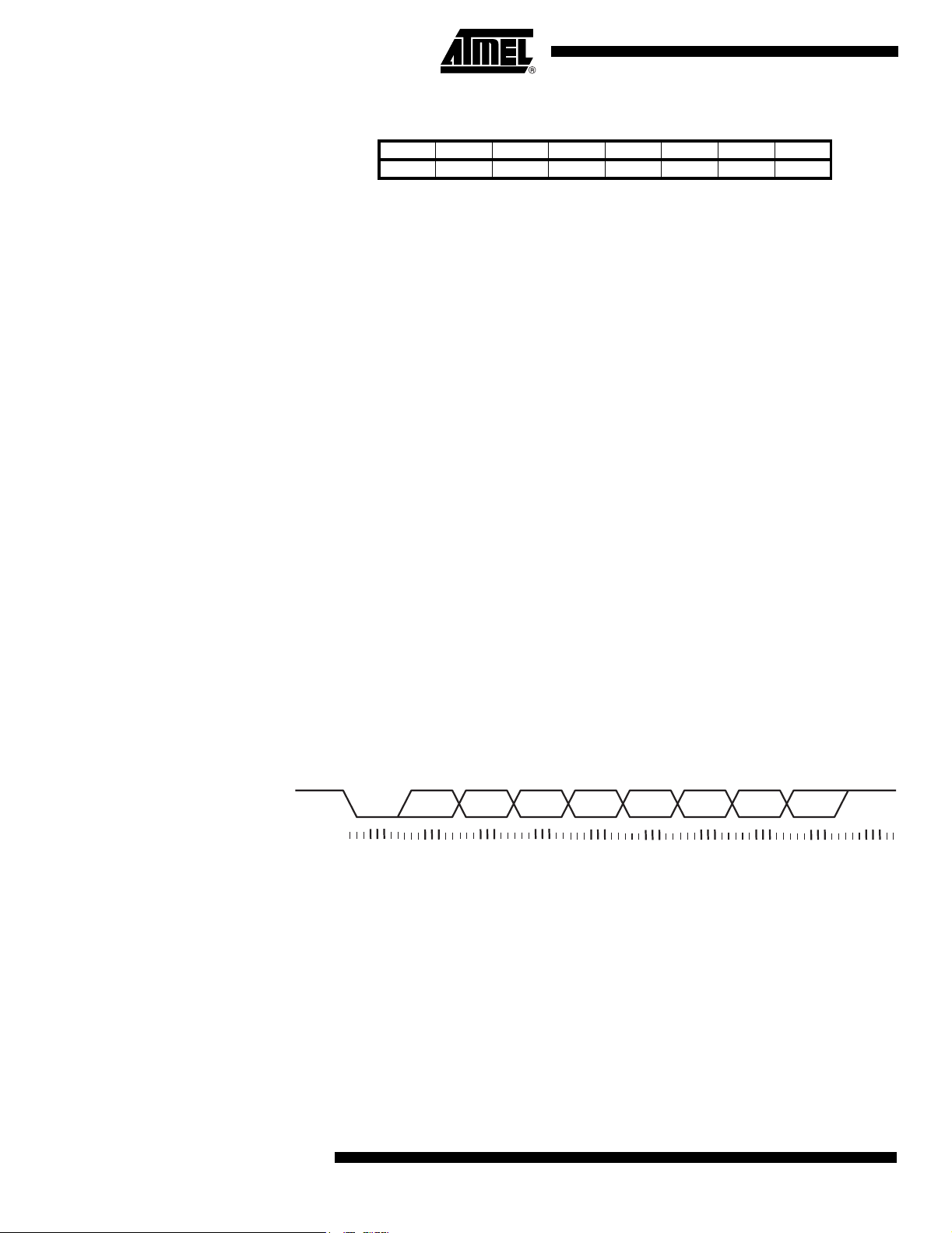
UART Baud Rate Registers – UBRR and UBRRHI
Bit 151413121110 9 8
$20 ($40) ––––MSB LSBUBRRHI
$09 ($29) MSB LSB UBRR
76543210
Read/Write R R R R R/W R/W R/W R/W
R/W R/W R/W R/W R/W R/W R/W R/W
Initial Value00000000
00000000
This is a 12-bit register which con tains the UART Baud Ra te according to the equation
on the previous page. The UBRRHI contains the fo ur most significant bits, and the
UBRR contains the eight least significant bits of the UART Baud Rate.
Double Speed Transmission
The ATmega1 63 pro vides a separa te UAR T mode which allows t he user to do uble the
communication speed. By setting the U2X bit in the UART Control and S tatus Register
UCSRA , the UAR T spe ed w ill be do ubled. Not e, ho wev er, th at the r ece iver will in this
case only use ha lf the nu mber of sampl es (only 8 i nstead o f 16) for data s amp ling and
clock recovery, and therefore requires m ore accurate baud rate setting and system
clock.
The data reception will differ slightly from Normal mode. Since the speed is doubled, the
Receiver front-end logic sam pl es the s ig nals on RX D pin at a freq uency ei ght time s t he
baud rate. While the line is idle , one single samp le of logical zero will be inte rpreted as
the falling edge of a start bit, and the start bit detection sequence is initiated. Let sample
1 denote the first zero-sample. Following the 1 to 0-transition, the Receiver samples the
RXD pin at sa mples 4, 5, an d 6. If two or m ore of these three sa mples a re found to be
logical ones, the start bit is rejected as a noise spike an d the receiver sta rts looking for
the next 1 to 0-transition.
If however, a valid start bit is detected , samplin g of the data bits following the start bit is
performed. These bits are als o samp led at s amp les 4, 5, an d 6. The lo gical valu e fou nd
in at least two of the three samples is taken as the bit value. All bits are shifted into the
Transmitter Shift Regis ter as they are sampled. Sampling of an incoming character is
shown in Figure 48.
Figure 48. Sampling Received Data When the Transmission Speed is Doubled
RXD
START BIT D0 D1 D2 D3 D4 D5 D6 D7 STOP BIT
RECEIVER
SAMPLING
The Baud Rate Generator in Double UART Speed Mode
78
ATmega163(L)
Note that the baud-rate equation is different from the equation on page 78 when the
UART speed is doubled:
f
CK
BAUD
----------------------------- -=
8(UBR 1)+
• BAUD = Baud Rate
•f
= Crystal Clock frequency
CK
• UBR = Contents of the UBRRHI and UBRR Registers, (0 - 4095)
• Note that this equation is only valid when the UART Transmission Speed is doubled.
For standard crystal frequencies, the most commonly used baud rates can be generated
by using the UBR settings in Table 28. UBR values which yield an actual baud rate differing less than 1.5% from the target baud rate, are bold in the table. However, since the
1142E–AVR–02/03
Page 79
ATmega163(L)
number of samples are reduced, and the system clock might have some variance (this
applies especially when using resonators), it is recommended that the baud rate error is
less than 0.5%.
Table 28. UBR Settings at Various Crystal Frequencies in Double Speed Mode
1.0000 MHz % E rror 1.8432 MHz % Error 2.0000 MHz % E rror
UBR = 51 0.2 UBR = 95 0 .0 UBR = 103 0.2
UBR = 25 0.2 UBR = 47 0 .0 UBR = 51 0.2
UBR = 12 0.2 UBR = 23 0 .0 UBR = 25 0.2
UBR = 8 3.7 UBR = 15 0.0 U B R = 16 2.1
UBR = 6 7.5 UBR = 11 0.0 UBR = 12 0.2
UBR = 3 7.8 UBR = 70.0UBR = 8 3.7
UBR = 2 7.8 UBR = 50.0UBR = 6 7.5
UBR = 1 7.8 UBR = 30.0UBR = 3 7.8
UBR = 1 22.9 UBR = 20.0UBR = 2 7.8
UBR = 0 84.3 UBR = 1 0.0 UBR = 1 7.8
--
3.2768 MHz % E rror 3.6864 MHz % Error 4.0000 MHz % E rror
UBR = 170 0.2 UBR = 191 0.0 UBR = 207 0.2
UBR = 84 0.4 UBR = 95 0 .0 UBR = 103 0.2
UBR = 42 0.8 UBR = 47 0 .0 UBR = 51 0.2
UBR = 27 1.6 UBR = 31 0.0 UBR = 34 0.8
UBR = 20 1.6 UBR = 23 0.0 UBR = 25 0.2
UBR = 13 1.6 UBR = 15 0.0 U BR = 16 2.1
UBR = 10 3.1 UBR = 11 0.0 UBR = 12 0.2
UBR = 6 1.6 UBR = 70.0UBR = 8 3.7
UBR = 4 6.2 UBR = 50.0UBR = 6 7.5
UBR = 3 12.5 UBR = 30.0UBR = 3 7.8
UBR = 1 12.5 UBR = 10.0UBR = 1 7.8
UBR = 0 12.5
UBR = 0
UBR = 0
0.0 --
0.0 UBR = 0 7.8
1142E–AVR–02/03
7.3728 MHz % E rror 8.0000 MHz % Error
UBR = 383 0.0 UBR = 416 0.1
UBR = 191 0.0 UBR = 207 0.2
UBR = 95 0.0 UBR = 103 0.2
UBR = 63 0.0 UBR = 68 0 .6
UBR = 47 0.0 UBR = 51 0 .2
UBR = 31 0.0 UBR = 34 0 .8
UBR = 23 0.0 UBR = 25 0 .2
UBR = 15 0.0 UBR = 16 2.1
UBR = 11 0.0 UBR = 12 0.2
UBR = 7 0.0 UBR = 8 3.7
UBR = 30.0UBR = 3 7.8
UBR = 1 0.0 UBR = 1 7.8
UBR = 0
0.0 UBR = 0 7.8
79
Page 80

Two-wir e S er ial Interface (Byte Oriented)
The Two-wire Serial Interface supports bi-directional serial communication. It is
designed primarily for si mple but efficien t integrated circ uit (IC) con trol. The system is
comprised of two lines, SCL (S erial Clock) and SDA (Serial Data) that carry information
between the ICs co nnected to them. Vario us communication con figurations can be
design ed usi ng t his b us. Figur e 4 9 show s a ty pica l Tw o-wire Se rial Bu s co nfigu rati on.
Any device connected to the bus can be master or slave. Note that all AVR devices connected to the bus must be powered to allow any bus operation.
Figure 49. Two-wire Serial Bus Configuration
V
CC
Device 1 Device 2 Device 3 Device n.......
R1 R2
SCL
SDA
The Two-wire Serial Interface supports Master/Slave and Transmitter/Receiver operation at up to 217 kHz bus clock rate. The Two-wire Serial Interface has hardware
support for 7-bit addressing, but is easily extended to, e.g., a 10-bit addressing format in
software. When the Two-wire Serial Interface is enabled (TWEN in TWCR is set), a
glitch filter is enabled for the input signals from the pins PC0 (SCL) and PC1 (SDA), and
the output from these pins is slew-rate controlle d. The Two-wire Serial Interface is byt e
oriented. The operation of the Tw o-wire Serial Bus is shown as a pulse diagram in Figure 50, including the START and ST OP c ondi tions and gen eration of ACK s ign al by the
bus receiver.
Figure 50. Two-wire Serial Bus Timing Diagram
ACKNOWLEDGE
FROM RECEIVER
SDA
SCL
START
CONDITION
MSB R/W
BIT
12 789 12 89
ACK ACK
STOP CONDITION
REPEATED START
CONDITION
80
The block diagram of the Two-wire Serial Interface is shown in Figure 51.
ATmega163(L)
1142E–AVR–02/03
Page 81

Figure 51. Block Diagram of the Two-wire Serial Interface
ADDRESS REGISTER
AND
COMPARATOR
TWAR
ATmega163(L)
SDA
SCL
INPUT
OUTPUT
INPUT
OUTPUT
DATA SHIFT
REGISTER
TWDR
START/STOP
AND SYNC
ARBITRATION
SERIAL CLOCK
GENERATOR
STATUS
STATE MACHINE
AND
STATUS DECODER
ACK
TIMING
AND
CONTROL
AVR 8-BIT DATA BUS
CONTROL
REGISTER
TWCR
STATUS
REGISTER
TWSR
1142E–AVR–02/03
The CPU interfaces with the Two-wire Serial Interface via the following five I/O Registers: the Two-wire Serial In terface Bit Rate Registe r (TWBR), the Two- wire Serial
Interface Control Register (TWCR), the Two-wire Serial Interface Status Register
(TWSR), the Two-wire Serial Interface Data Regi ster (TWDR), and the Tw o-wire Serial
Interface Address Register (TWAR, used in Slave mode).
81
Page 82

The Two-wire Serial Interface Bit Rate Register – TWBR
Bit 76543210
$00 ($20) TWBR7 TWBR6 TWBR5 TWBR4 TWBR3 TWBR2 TWBR1 TWBR0 TWBR
Read/Write R/W R/W R/W R/W R/W R/W R/W R/W
Initial Value00000000
• Bits 7..0 – Two-wire Serial Interface Bit Rate Register
TWBR selects the division factor for the bit rate generator. The bit rate generator is a
frequency divider which generates the SCL clock frequency in the Master modes
according to the following equation:
f
Bit Rate
-----------------------------------------------------------=
16 2(TWBR) + tAf
+
CK
CK
• Bit Rate = SCL frequency
•f
= CPU Clock frequency
CK
• TWBR = Contents of the Two-wire Serial Interface Bit Rate Register
= Bus alignment adjustion
•t
A
Note: Both the Receiver and the Trans mitter can stretch the low period of the SCL line when
waiting for user resp onse, thereby reducing the average bit rate.
TWBR should be set to a value higher than seven to ensure correct Two-wire Serial Bus
functionality. The bus alignment adj ustion is automatically inserted by the Two-wire
Serial Interface, and ensures the validity of setup and hold times on the bus for any
TWBR value higher than seven. This adjustment may vary from 200 ns to 600 ns
depending on bus loads and drive capabilities of the devices connected to the bus.
The Two-wire Serial Interface Control Register – TWCR
Bit 76543210
$36 ($56) TWINT TWEA TWSTA TWSTO TWWC TWEN – TWIE TWCR
Read/Write R/W R/W R/W R/W R R/W R R/W
Initial Value00000000
• Bit 7 – TWINT: Two-wire Serial Interface Interrupt Flag
This bit is set by hardware when the Two-wire Serial Interface has finished its current
job and expects ap plication soft ware res ponse. I f the I-bit in the S RE G and TWIE in the
TWCR Register are set (one), the MCU will jump to the Interrupt Vector at address $22.
While the TWINT Flag is set, the bus SCL clock line low period is stretched. The TWINT
Flag must be cleared by software by writing a logic one to it. Note that this flag is not
automaticaly cleared by hardware when executing the interrupt routine. Also note that
clearing this flag starts the operation of the Two-wire Serial Interface, so all accesses to
the Two-wire Serial Interface Address Register – TWAR, Two-wire Serial Interface Status Register – TWSR, and Two-wire Serial Interface Data Register – TWDR must be
complete before clearing this flag.
82
ATmega163(L)
1142E–AVR–02/03
Page 83

ATmega163(L)
• Bit 6 – TWEA: Two-wire Serial Interface Enable Acknowledge Flag
TWEA Flag controls the generation of the acknowledge pulse. If the TWEA bit is set,
the ACK pulse is generated on the Two-wire Serial Bus if the following conditions are
met:
1. The device’s own slave address has been received.
2. A general call has been received, while the TWGCE bit in the TWAR is set.
3. A data byte has been received in Master Receiver or Slave Receiver mode.
By setting the TWEA bit low, the device can be virtually disconnected from the Two-wire
Serial Bus temporarily. Addre ss recognition can then be resumed by setting the TWEA
bit again.
• Bit 5 – TWSTA: Two-wire Serial Bus START Condition Flag
The TW ST A Fl ag i s se t by the appl icat io n whe n it des ires to b eco me a Ma ste r o n the
Two-wire Serial Bus. The Two-wire Serial Interface hardware checks if the bus is available, and generates a START condition on the bus if it is free. However, if the bus is not
free, the Two-wire Serial Interface waits until a STOP condition is detected, and then
generates a new START condition to claim the bus Master status.
• Bi t 4 – TW ST O: Two-wire Seria l Bus S TO P Condition Fl ag
TWSTO is a Stop Condition Flag. In Master mode setting the TWST O bit in the Control
Registe r will ge ne rate a S TO P con dition on the Two-w ir e Seria l Bus. When the STOP
condition is executed on the bus, the TWSTO bit is cleared automatically. In Slave mode
setting the TWSTO bit can be used to recover from an error condition. No stop condition
is generated on the bus then, but th e Two-wire Serial Inte rface returns to a well-defined
unaddressed Slave mode and releases the SCL and SDA lines to a high impedance
state.
• Bit 3 – TWWC: Two-wire Serial Bus Write Collision Flag
The TWWC bit is set when attempting to write to the Two-wire Serial Interface Data
Register – TWDR when TWINT is low. This flag is cleared by writing t he TWDR Register
when TWINT is high.
• Bit 2 – TWEN: Two-wire Serial Interface Enable Bit
The TWEN bit en able s Two-wi re Seria l Inte rface operati on. If t his bit is cleare d (zero),
the bus outputs SDA and SCL are set to high impedance state, and the input signals are
ignored. The interface is activated by setting this bit (one).
• Bit 1 – Res: Reserved Bit
This bit is a reserved bit in the ATmega163 and will always read as zero.
1142E–AVR–02/03
83
Page 84

• Bi t 0 – TWIE: Two-wi re Ser ial Interface Interru pt En able
When this bit is enabled, and the I-bit in SREG is set, the Two-wire Serial Interface interrupt will be a c ti v a ted for as long as the TWINT Fla g is high.
The TWCR is used to control the operation of the Two-wire Serial Interface. It is used to
enable the T w o-wire Se rial In terface , to in itiate a M aster a ccess by ap plyin g a STA RT
condition to the bus, to ge nerate a receiver acknow ledge, to gene rate a stop cond ition,
and to control halting of the bus while th e dat a to be written to the bu s are written to the
TWDR. It also indica tes a write collisio n if data is attem pted written to TWDR whil e the
register is inaccessible.
The Two-wire Serial Interface Status Register – TWSR
The Two-wire Serial Interface Data Register – TWDR
Bit 76543210
$01 ($21) TWS7 TWS6 TWS5 TWS4 TWS3 – – – TWSR
Read/Write R RRRRRRR
Initial Value11111000
• Bits 7..3 – TWS: Two-wire Serial Interface Status
These five bits reflect the status of the Two-wire Serial Interface logic and the Two-wire
Serial Bus.
• Bits 2..0 – Res: Reserved bits
These bits are reserved in ATmega163 and will always read as zero
The TWS R is read on ly. It co ntains a s tatus co de wh ich reflect s the stat us of the Two-
wire Serial Interface logic and the Two-wire Serial Bus. There are 26 possible status
codes. When TWSR contains $F8, no relevant state information is available and no
Two-wire S erial Interface i nterrupt is re quested. A val id status code is availab le in
TWSR one CPU clock cycle after the Two-wire Serial Interface Interrupt Flag ( TWINT) is
set by hardw are and is va lid un til one CPU cloc k cy cle afte r TWINT is clea red by software. Table 32 to Table 36 give the status information for the various modes.
Bit 76543210
$03 ($23) TWD7 TWD6 TWD5 TWD4 TWD3 TWD2 TWD1 TWD0 TWDR
Read/Write R/W R/W R/W R/W R/W R/W R/W R/W
Initial Value11111111
84
• Bit s 7..0 – TWD: Two-wire Se ria l Interface Data Register
These eight bits constitute the next data byte to be transmitted, or the latest data byte
received on the Two-wire Serial Bus.
In Transmit mode, TWDR contains the next byte to be transmitted. In Receive mode, the
TWDR contains the last byte received. It is writeable while the Two-wire Serial Interface
is not in th e proces s of shifting a byte . This occ urs wh en the Two -wire S erial I nterfa ce
Interrupt Flag (TWINT) is set by hardware. Note that the Data Register cannot be initialized by the u ser be fore the fi rst interr upt occu rs. The data in TW DR rema in stab le as
long as TWINT is set. While data is shifted out, data on the bus is simultaneously shifted
in. TWDR always contains the last byte present on the bus, except after a wake up from
ADC Noise Reduction m ode, P owe r-down m ode, or Po wer-save m ode by the Two-wire
Serial I nter fac e i nterru pt. F or e xam pl e, in the cas e of a los t bu s ar bitr atio n, n o da ta is
lost in the transition from Maste r to Slave. Handli ng of the ACK Flag is cont rolled automatically by the Two-wire Serial Interface logic, the CPU cannot access the ACK bit
directly.
ATmega163(L)
1142E–AVR–02/03
Page 85

ATmega163(L)
The Two-wire Serial Interface (Slave) Address Register – TWAR
Two-wire Ser ial I nte rface Modes
Bit 76543210
$02 ($22) TWA6 TWA5 TWA4 TWA3 TWA2 TWA1 TWA0 TWGCE TWAR
Read/Write R/W R/W R/W R/W R/W R/W R/W R/W
Initial Value11111110
• Bit s 7..1 – TWA: Two-wire Se rial Interface (Slave ) Address Regis ter
These seven bits constitute the slave address of the Two-wire Serial Bus unit.
• Bit 0 – TWGCE: Two-wire Serial Interface General Call Recognition Enable Bit
This bit enables, if set, the recognition of the General Call given over the Two-wire Serial
Bus.
The TWAR should be loaded with the 7-bit slave address (in the seven most significant
bits of TWAR) to which the Two-wire Serial Interface will respond when programmed as
a Slave Transmitter or Receiver, and not needed in the Master modes . The LSB of
TWAR is used to enable recognition of the general call address ($00). There is an associated address comparator that looks for the slave address (or generall c all address if
enabled) in the received s erial address. If a match is found, an interrupt request is
generated.
The Two-wire Serial Interface can operate in four different modes:
• Master Transmitter
• Master Receiver
•Slave Receiver
• Slave Transmitter
Data transfer in each mod e of op eration is s hown in Figure 52 to Figure 55. Th ese fig -
ures contain the following abbreviations:
S: START condition
R: Read bit (high level at SDA)
W: Write bit (low level at SDA)
A: Acknowledge bit (low level at SDA)
: Not acknowledge bit (high level at SDA)
A
Data: 8-bit data byte
P: STOP condition
SLA: Slave Address
In Figure 52 to Figure 55, circles are used to indicate that the Two-wire Serial Interface
Interrupt Flag is set. The num bers in the circles s how the status code held in T WS R. At
these points, actions m ust be taken by the application to continue or compl ete the T wowire Serial Bu s trans fer. The Tw o-wire Se rial Bu s transf er is susp en ded unti l the Tw owire Serial Interface Interrupt Flag is cleared by software.
The Two-wire Serial Interface Interrupt Flag is not automatically cleared by hardware
when executing the interrupt routine. Software has to clear the flag to continue the Twowire tr an sfer . Als o not e tha t th e Tw o-w ire S eri al In terfa ce star ts ex ecu ti on as soo n as
this bit is cleared, so that all access to TWAR, TWDR, and TWSR must have been completed before clearing this flag.
1142E–AVR–02/03
85
Page 86

When the Two-wire Serial Interface Interrupt Flag is set, the status code in TWSR is
used to determine the appropriate software action. For each status code, the required
software action and details of the following serial transfer are given in Table 32 to Table
36.
Master Transmitter Mode In th e Master Transmitter mode, a number of data bytes are transmitted to a Slave
Receiver (see Figure 52). Before M aster Trans mitter m ode can be entered , the TWC R
must be initialized as follows:
Table 29. TWCR: Master Transmitter Mode Initialization
TWCR TWINT TWEA TWSTA TWSTO TWWC TWEN – TWIE
Value
TWEN must be se t to en able the Tw o-wire Serial In terface, TWS TA and TWSTO m ust
be cleared.
The Master Transmitter mode may now be entere d by setting the TWS T A bit. The Tw owire Seria l Interfa ce logic w ill then test the T wo-wire Serial Bus and generate a START
condition as soon as the bus becomes free. When a START condition is transmitted, the
Two-wire Serial Interface Interrupt Flag (TWINT) is set by hardware, and t he st atus c ode
in TWSR w ill be $08 . TWD R mus t then be load ed with t he slave addr ess an d the dat a
direction bit (SLA+W). Clearing the TWINT bit in software will continue the transfer. The
TWINT Flag is cleared by writing a logic one to the flag.
When the slav e address and the direction bit have been transmitted and an ac knowledgement bit has been received, TWINT is set again and a number of status codes in
TWSR are possible. Possible status codes in Master mode are $18, $20, or $38. The
appropriate action to be taken for each of these status codes is detailed in Table 32. The
data must be loaded when TWI NT is hi gh onl y. I f not, the access will be discar ded, and
the Write Collision bit – TWWC will be set in the TWCR Register. This scheme is
repeated until the last byte is sent and the transfer is ended by generating a STOP c ondition or a repeated START condition. A STOP condition is generated by setting
TWSTO, a repeated START condit ion is generated by setting TWSTA and TW STO.
0 X00010 X
After a repeated START condition (state $10) the Two-wire Serial Interface can acces s
the same Slave again, or a new Slave without transmitting a STOP condition. Repeated
START enables the Master to switch between Slaves, Master Transmitter mode and
Master Receiver mode without loosing control over the bus.
Assembly code illustrating operatio n of the Mas ter Trans mitter mod e is given at the end
of the TWI section.
Master Receiver Mode I n the Master Receiver mo de, a number of data byt es are rec ei ved f rom a S lave Trans -
mitter (see Figure 53). The transfer is initialized as in the Master Transmitter mode.
When the S TART co ndit ion has b een transmit ted, the T WIN T Flag is s et by h ardware.
The software must then load T WDR with the 7-bit slave address and the Data Direction
bit (SLA+R). The transfer will then continue when the TWINT Flag is cleared by
software.
When the slav e address and the direction bit have been transmitted and an ac knowledgement bit has been received, TWINT is set again and a number of status codes in
TWSR are possible. Possible status codes in Master mode are $40, $48, or $38. The
appropriate action to be taken for each of these status codes is detailed in Table 52.
Received d ata can be read fr om the TWDR Re gister w hen the T WINT Flag is s et high
by hardware. This scheme is repeated until the last byte has been received and a STOP
condition is transmitted by writing a logic one to the TWSTO bit in the TWCR Register.
86
ATmega163(L)
1142E–AVR–02/03
Page 87

ATmega163(L)
After a repeated START c ondition (state $10), the Two-wire S erial Interface may switc h
to the Master Transm itter mode by loading TW DR with SLA+ W or acces s a new Slave
as Master Receiver or Transmitter.
Assembly code illustrating opera tion of the Mas ter Receiver mode is gi ven at the end of
the TWI section.
Slave Receiver Mode In the Slave Receiver mode, a number of data bytes are received from a Master Trans-
mitter (see Figure 54). To initiate the Slave Receiver mode, TWAR and TWCR must be
initialized as follows:
Table 30. TWAR: Slave Receiver Mode Initialization
TWAR TWA6 TWA5 TWA4 TWA3 TWA2 TWA1 TWA0 TWGCE
Value
The upper seven bits are the address to which the Two-wire Serial Interface will respond
when addressed by a Master. If the LSB is set, the Two-wire Serial Interface will
respon d to th e gen eral cal l addr ess ($0 0), oth erwis e it will ignore the ge neral ca ll
address.
Table 31. WCR: Slave Receiver Mode Initialization
TWCR TWINT TWEA TWSTA TWSTO TWWC TW EN – TWIE
Value
0 100010 X
Device’s Own Slave Address
TWEN must be set to enable the Two-wire Serial Interface. The TWEA bit must be set to
enable the acknowledgem ent of the device’s own slave address or the general call
address. TWSTA and TWSTO m ust be cleared.
When TWAR and TWC R have been initialized, the Two-wi re Serial Interface waits until
it is addressed by its own slave address (or the general call address if enabled) followed
by the D at a Dir ectio n bit whic h must be “0” (w rite ) for th e Two -wire Seri al Inte rfa ce to
operate in the Slave Rece iver mode. After its ow n slave address an d the write bit have
been received, the Two-wire Serial Interface Interrupt Flag is set and a valid status code
can be read from TWSR. The status code is used to determine the appropriate software
action. The app ropriat e action to be taken for ea ch statu s code is detailed in Table 34.
The Slav e Rec eiver m ode may a lso be en tered i f arb itrat ion is lo st wh ile the Two- wire
Serial Interface is in the Master mode (see states $68 and $78).
If the TWEA bit is reset during a transfer, the Two-wire Serial Interface will return a “Not
Acknowledge” (“1”) to SDA after the next received data byte. W hile TWEA is Reset, the
Two-wire Serial Interface does not respond to its own slave address. However, the Twowire Serial Bus is still monitored and address recognition may resume at any time by
setting TWEA. This implies that the TWEA bit may be used to temporarily isolate the
Two-wire Serial Interface from the Two-wire Serial Bus.
In ADC Noise Reduction mode, Power-down mode, and Power-save mode, the clock
system to the Two-wire Serial Interface is turned off. If the Slave Receive mode is
enabled, the interface can still acknowledge a general call and its own slave address by
using the Two-wire Serial Bus clock as a clock source. The part will then wake-up from
sleep and the Tw o-w i re Se rial I nt er face will hold the SC L clock wil low during the wakeup and until the TWINT Flag is cleared.
1142E–AVR–02/03
Note that the Two-wire Serial Interface Data Register – TWDR – does not reflect the last
byte present on the bus when waking up from these sleep modes.
Assembly c ode illustra ting operatio n of the S lave Rec eiver mo de is given a t the end of
the TWI section.
87
Page 88

Slave Transmitter Mode In the Slave Transmi tter mode, a number of data bytes are transmitted to a Master
Receiver (see Figure 55). The transfer is initialized as in the Slave Receiver mode.
When TWAR and TWC R have been initialized, the Two-wi re Serial Interface waits until
it is addressed by its own slave address (or the general call address if enabled) followed
by the Data Direction bit which must be “1” (read) for the Two-wire Serial Interface to
operate in the Slave Transmitter mode. After its own slave address and the read bit
have been received, the Two-wire Serial Interface Interrupt Flag is set and a valid status
code can be read from TWSR. The status code is used to determine the appropriate
softwa re ac tion . Th e app ropri ate acti on to be take n for e ach statu s co de is deta ile d in
Table 35. The slave transm itter mod e m ay also be entered if arbitration i s lost while t he
Two-wire Serial Interface is in the Master mode (see state $B0).
If the TWEA bit is reset during a transfer, the Two-wire Serial Interface will transmit the
last byte of the transfer and enter state $C0 or state $C8. the Two-wire Serial Interface
is switched t o the not address ed S lave mod e, and will igno re the Maste r if it cont inues
the transfer. Thus the Master Receiver receives all “1” as serial data. While TWEA is
reset, the Two-wire Serial Interface does not respond to its own slav e address. However, the Two-wire Serial Bus is still monitored and address recognition may resume at
any tim e by s ettin g TWEA . Thi s imp lies tha t the T W EA bi t may be use d to te mpor arily
isolate the Two-wire Serial Interface from the Two-wire Serial Bus.
Assembly c ode illustra ting operatio n of the S lave Rec eiver mo de is given a t the end of
the TWI section.
Miscellaneous States There are two status codes that do not correspond to a defined Two-wire Serial Inter-
face state, see Table 36.
Status $F8 indicates that no relevant information is available because the Two-wire
Serial Interface Interrupt Flag (TWINT) is not set y et. This occ urs between other states,
and when the Two-wire Serial Interface is not involved in a serial transfer.
Status $00 indicates that a bus error has occured during a Two-wire Serial Bus transfer.
A bus error occurs when a STAR T or STOP co ndit ion occ urs at an illeg al pos it ion in t he
format fra me. Exa mples of suc h illegal p ositions ar e during the s erial trans fer of an
address byte, a data byte or an acknowledge bit. When a bus error occurs, TWINT is
set. To recover from a bus error, the TWSTO Flag must set and TWINT must be cleared
by writing a logic one to it. This causes the Two-wire Serial Interface to enter the not
addressed Slave mode and to clear the TWSTO Flag (no other bits in TWCR are
affected). The SDA and SCL lines are released and no STOP condition is transmitte d.
88
ATmega163(L)
1142E–AVR–02/03
Page 89

Table 32. St atus Codes for Master Transmitter Mode
Status Code
(TWSR)
$08 A START condition has been
$10 A repeated START condition
$18 SLA+W has been transmitted;
$20 SLA+W has been transmitted;
$28 Data byte has been transmitted;
$30 Data byte has been transmitted;
$38 Arbitration lost in SLA+W or
Status of the Two-wire Serial
Bus and Two-wire Serial Interface Hardware
transmitted
has been transmitted
ACK has been received
NOT ACK has been received
ACK has been received
NOT ACK has been received
data bytes
To/from TWDR
Load SLA+W X 0 1 X SLA+W will be transmitted;
Load SLA+W or
Load SLA+R
Load data byte or
No TWDR action or
No TWDR action or
No TWDR action
Load data byte or
No TWDR action or
No TWDR action or
No TWDR action
Load data byte or
No TWDR action or
No TWDR action or
No TWDR action
Load data byte or
No TWDR action or
No TWDR action or
No TWDR action
No TWDR action or
No TWDR action
Application Software Response
To TWCR
STA STO TWINT TWEA
X
0
X
0
0
0
0
1
1
0
1
1
0
0
0
1
1
0
1
1
0
0
0
1
1
0
1
1
0
0
0
1
1
0
1
1
0
0
1
0
1
1
1
1
1
1
1
1
1
1
1
1
1
1
1
1
1
1
1
1
XXSLA+W will be transmitted;
X
X
X
X
X
X
X
X
X
X
X
X
X
X
X
X
XXTwo-wire Serial Bus will be released and not addressed
ATmega163(L)
Next Action Taken by Two-wire Serial Interface Hardware
ACK or NOT ACK will be received
ACK or NOT ACK will be received
SLA+R will be transmitted;
Logic will switch to Master Receiver mode
Data byte will be transmitted and ACK or NOT ACK will
be received
Repeated START will be transmitted
STOP condition will be transmitted and
TWSTO Flag will be Reset
STOP condition followed by a START condition will be
transmitted and TWSTO Flag will be reset
Data byte will be transmitted and ACK or NOT ACK will
be received
Repeated START will be transmitted
STOP condition will be transmitted and
TWSTO Flag will be Reset
STOP condition followed by a START condition will be
transmitted and TWSTO Flag will be Reset
Data byte will be transmitted and ACK or NOT ACK will
be received
Repeated START will be transmitted
STOP condition will be transmitted and
TWSTO Flag will be Reset
STOP condition followed by a START condition will be
transmitted and TWSTO Flag will be Reset
Data byte will be transmitted and ACK or NOT ACK will
be received
Repeated START will be transmitted
STOP condition will be transmitted and
TWSTO Flag will be Reset
STOP condition followed by a START condition will be
transmitted and TWSTO Flag will be Reset
Slave mode entered
A START condition will be transmitted when the bus becomes free
1142E–AVR–02/03
89
Page 90

Figure 52. Formats and States in the Master Transmitter Mode
MT
Successfull
Transmission
to a Slave
Receiver
S SLA W A DATA A P
$08
Next T ransf er
Started with a
Repeated Start
Condition
Not Acknowledge
Received After the
Slave Address
Not Acknowledge
Received After a Data
Byte
Arbitration Lost in Slave
Address or Data Byte
Arbitration Lost and
Addressed as Slave
$18 $28
AP
$20
Other Master
A or A
Continues
A or A
$38
Other Master
A
Continues
A
$30
$38
S SLA W
$10
P
Other Master
Continues
R
MR
Assembly Code Example – Master Transmitter Mode
To Corresponding
States in Slave Mode
Any Number of Data Bytes
and their Associated Acknowledge Bits
This Number (Contained in TWSR) Corresponds
to a Defined State of the Two-wire Serial Bus
From Master to Slave
From Slave to Master
$68
$78 $B0
DATA A
n
;The Slave being addressed has address 0x64. The code examples also assumes
some sort of error handling routine named ERROR.
;Part specific include file and TWI include file must be included.
; <Initialize registers, including TWAR, TWBR and TWCR>
ldi r16, (1<<TWSTA) | (1<<TWEN)
out TWCR, r16 ; Send START condition
wait1: in r16,TWCR ; Wait for TWINT Flag set. This indicates that
sbrs r16,TWINT ; the START condition has been transmitted
rjmp wait1
in r16, TWSR ; Check value of TWI Status Register.
cpi r16, START ; If status different from START go to ERROR
90
ATmega163(L)
1142E–AVR–02/03
Page 91

ATmega163(L)
brne ERROR
ldi r16, 0xc8 ; Load SLA+W into TWDR Register
out TWDR, r16
ldi r16, (1<<TWINT) | (1<<TWEN)
out TWCR, r16 ; Clear TWINT bit in TWCR to start transmission of
address
wait2:in r16, TWCR ; Wait for TWINT Flag set. This indicates that
sbrs r16, TWINT ; SLA+W has been transmitted, and ACK/NACK has
rjmp wait2 ; been received
in r16, TWSR ; Check value of TWI Status Register. If status
cpi r16, MT_SLA_ACK; different from MT_SLA_ACK, go to ERROR
brne ERROR
ldi r16, 0x33 ; Load data (here, data = 0x33) into TWDR Register
out TWDR, r16
ldi r16, (1<<TWINT) | (1<<TWEN)
out TWCR, r16 ; Clear TWINT bit in TWCR to start transmission of data
wait3:in r16, TWCR ; Wait for TWINT flag set. This indicates that
sbrs r16, TWINT; data has been transmitted, and ACK/NACK has
rjmp wait3 ; been received
in r16, TWSR ; Check value of TWI Status Register. If status
cpi r16, MT_DATA_ACK ; different from MT_DATA_ACK, go to ERROR
brne ERROR
ldi r16, 0x44 ; Load data (here, data = 0x44) into TWDR Register
out TWDR, r16
ldi r16, (1<<TWINT) | (1<<TWEN)
out TWCR, r16 ; Clear TWINT bit in TWCR to start transmission of data
;<send more data bytes if needed>
wait4:in r16, TWCR ; Wait for TWINT flag set. This indicates that
sbrs r16, TWINT; data has been transmitted, and ACK/NACK has
rjmp wait4 ; been received
in r16, TWSR ; Check value of TWI Status Register. If status
cpi r16, MT_DATA_ACK; different from MT_DATA_ACK, go to ERROR
brne ERROR
1142E–AVR–02/03
ldi r16, (1<<TWINT) | (1<<TWSTO) | (1<<TWEN)
out TWCR, r16 ; Transmit STOP condition
91
Page 92

Table 33. St atus Codes for Master Receiver Mode
Status Code
(TWSR)
$08 A START condition has been
$10 A repeated START condition
$38 Arbitration lost in SLA+R or
$40 SLA+R has been transmitted;
$48 SLA+R has been transmitted;
$50 Data byte has been received;
$58 Data byte has been received;
Status of the Two-wire Serial
Bus and Two-wire Serial Interface hardware
transmitted
has been transmitted
NOT ACK bit
ACK has been received
NOT ACK has been received
ACK has been returned
NOT ACK has been returned
To/from TWDR
Load SLA+R X 0 1 X SLA+R will be transmitted
Load SLA+R or
Load SLA+W
No TWDR action or
No TWDR actio
No TWDR action or
No TWDR action
No TWDR action or
No TWDR action or
No TWDR action
Read data byte or
Read data byte
Read data byte or
Read data byte or
Read data byte
Application Software Response
To TWCR
STA STO TWINT TWEA
X
0
X
0
0
0
1
0
0
0
0
0
0
1
1
0
1
1
0
0
0
0
0
1
1
0
1
1
1
XXSLA+R will be transmitted
1
1
XXTwo-wire Serial Bus will be released and not addressed
1
1
01Data byte will be received and NOT ACK will be
1
1
1
1
1
X
X
X
01Data byte will be received and NOT ACK will be
1
1
1
1
X
X
X
Next Action Taken by Two-wire Serial Interface Hardware
ACK or NOT ACK will be received
ACK or NOT ACK will be received
SLA+W will be transmitted
Logic will switch to Master Transmitter mode.
Slave mode will be entered
A START condition will be transmitted when the bus
becomes free
returned
Data byte will be received and ACK will be returned
Repeated START will be transmitted
STOP condition will be transmitted and TWSTO Flag
will be Reset
STOP condition followed by a START condition will be
transmitted and TWSTO Flag will be Reset
returned
Data byte will be received and ACK will be returned
Repeated START will be transmitted
STOP condition will be transmitted and TWSTO Flag
will be Reset
STOP condition followed by a START condition will be
transmitted and TWSTO Flag will be Reset
Figure 53. Formats and States in the Master Receiver Mode
MR
Successfull
Reception
From a Slave
Receiver
Next T ransf er
Started with a
Repeated Start
Condition
Not Acknowledge
Received After the
Slave Address
Arbitration Lost in Slave
Address or Data Byte
Arbitration Lost and
Addressed as Slave
S SLA R A DATA A
$08
From Master to Slave
From Slave to Master
$40 $50
AP
$48
Other Master
A or A
Continues
$38
Other Master
A
Continues
$68
$78 $B0
DATA A
n
Any Number of Data Bytes
and their Associated Acknowledge Bits
This Number (Contained in TWSR) Corresponds
to a Defined State of the Two-wire Serial Bus
Other Master
A
Continues
$38
To corresponding
states in slave mode
PDATA A
$58
S SLA R
$10
W
MT
92
ATmega163(L)
1142E–AVR–02/03
Page 93

ATmega163(L)
Assembly Code Example – Master Receiver Mode
;Part specific include file and TWI include file must be included.
; <Initialize registers TWAR and TWBR>
ldi r16, (1<<TWINT) | (1<<TWSTA) | (1<<TWEN)
out TWCR, r16 ;Send START condition
wait5:in r16,TWCR ; Wait for TWINT flag set. This indicates that
sbrs r16, TWINT ; the START condition has been transmitted
rjmp wait5
in r16, TWSR ; Check value of TWI Status Register. If status
cpi r16, START ; different from START, go to ERROR
brne ERROR
ldi r16, 0xc9 ; Load SLA+R into TWDR Register
out TWDR, r16
ldi r16, (1<<TWINT) | (1<<TWEN)
out TWCR, r16 ; Clear TWINT bit in TWCR to start transmission of
; SLA+R
wait6:in r16,TWCR ; Wait for TWINT flag set. This indicates that
sbrs r16, TWINT ; SLA+R has been transmitted, and ACK/NACK has
rjmp wait6 ; been received
in r16, TWSR ; Check value of TWI Status Register. If status
cpi r16, MR_SLA_ACK; different from MR_SLA_ACK, go to ERROR
brne ERROR
ldi r16, (1<<TWINT) | (1<<TWEA) | (1<<TWEN)
out TWCR, r16 ; Clear TWINT bit in TWCR to start reception of
; data.
; Setting TWEA causes ACK to be returned after
; reception of data byte
wait7:in r16,TWCR ; Wait for TWINT flag set. This indicates that
sbrs r16, TWINT ; data has been received and ACK returned
rjmp wait7
in r16, TWSR ; Check value of TWI Status Register. If status
cpi r16, MR_DATA_ACK ; different from MR_DATA_ACK, go to ERROR
brne ERROR
in r16, TWDR ; Input received data from TWDR.
nop ;<do something with received data>
ldi r16, (1<<TWINT) | (1<<TWEA) | (1<<TWEN)
out TWCR, r16 ; Clear TWINT bit in TWCR to start reception of
; data. Setting TWEA causes ACK to be returned
; after reception of data byte
;<Receive more data bytes if needed>
1142E–AVR–02/03
;receive next to last data byte.
wait8:in r16,TWCR ; Wait for TWINT flag set. This indicates that
93
Page 94

sbrs r16, TWINT ; data has been received and ACK returned
rjmp wait8
in r16, TWSR ; Check value of TWI Status Register. If status
cpi r16, MR_DATA_ACK ; different from MR_DATA_ACK, go to ERROR
brne ERROR
in r16, TWDR ; Input received data from TWDR.
nop ;<do something with received data>
ldi r16, (1<<TWINT) | (1<<TWEN)
out TWCR, r16 ; Clear TWINT bit in TWCR to start reception of
; data. Not setting TWEA causes NACK to be
; returned after reception of next data byte
; receive last data byte. Signal this to slave by
; returning NACK
wait9:in r16,TWCR ; Wait for TWINT flag set. This indicates that
sbrs r16, TWINT ; data has been received and NACK returned
rjmp wait9
in r16, TWSR ; Check value of TWI Status Register. If status
cpi r16, MR_DATA_NACK ; different from MR_DATA_NACK, go to ERROR
brne ERROR
in r16, TWDR ; Input received data from TWDR.
nop ;<do something with received data>
ldi r16, (1<<TWINT) | (1<<TWSTO) | (1<<TWEN)
out TWCR, r16 ; Send STOP signal
94
ATmega163(L)
1142E–AVR–02/03
Page 95

Table 34. St atus Codes for Slave Receiver Mode
Status code
(TWSR)
$60 Own SLA+W has been received;
$68 Arbitration lost in SLA+R/W as
$70 General call address has been
$78 Arbitration lost in SLA+R/W as
$80 Previously addressed with own
$88 Previously addressed with own
$90 Previously addressed with
$98 Previously addressed with
$A0 A STOP condition or repeated
Status of the Two-wir e Ser ial Bu s
and Two-wire Serial Interface
hardware
ACK has been returned
master; own SLA+W has been
received; ACK has been returned
received; ACK has been returned
master; General call address ha s
been received; ACK has been
returned
SLA+W; data has been received;
ACK has been returned
SLA+W; data has been received;
NOT ACK has been returned
general call; data has been received; ACK has been returned
general call; data has been
received; NOT ACK has been
returned
START condition has been
received while still addressed a s
slave
To/from TWDR
No TWDR action or
No TWDR action
No TWDR action or
No TWDR action
No TWDR action or
No TWDR action
No TWDR action or
No TWDR action
Read data byte or
Read data byte
Read data byte or
Read data byte or
Read data byte or
Read data byte
Read data byte or
Read data byte
Read data byte or
Read data byte or
Read data byte or
Read data byte
Read data byte or
Read data byte or
Read data byte or
Read data byte
Application Software Response
To TWCR
STA STO TWINT TWEA
X
0
X
0
X
0
X
0
X
0
X
0
X
0
X
0
X
0
X
0
0
0
0
0
1
0
1
0
X
0
X
0
0
0
0
0
1
0
1
0
0
0
0
0
1
0
1
0
ATmega163(L)
Next Action Taken by Two-wire Serial Interface Hardtware
1
1
1
1
1
1
1
1
1
1
1
1
1
1
1
1
1
1
1
1
1
1
1
1
01Data byte will be received and NOT ACK will be
returned
Data byte will be received and ACK will be returned
01Data byte will be received and NOT ACK will be
returned
Data byte will be received and ACK will be returned
01Data byte will be received and NOT ACK will be
returned
Data byte will be received and ACK will be returned
01Data byte will be received and NOT ACK will be
returned
Data byte will be received and ACK will be returned
01Data byte will be received and NOT ACK will be
returned
Data byte will be received and ACK will be returned
0
Switched to the not addressed Slave mode;
no recognition of own SLA or GCA
1
Switched to the not addressed Slave mode;
own SLA will be recognized;
GCA will be recognized if TWGCE = “1”
Switched to the not addressed Slave mode;
0
no recognition of own SLA or GCA;
a START condition will be transmitted when the bus
becomes free
Switched to the not addressed Slave mode;
1
own SLA will be recognized;
GCA will be recognized if TWGCE = “1”;
a START condition will be transmitted when the bus
becomes free
0
Switched to the not addressed Slave mode;
no recognition of own SLA or GCA
1
Switched to the not addressed Slave mode;
own SLA will be recognized;
GCA will be recognized if TWGCE = “1”
Switched to the not addressed Slave mode;
0
no recognition of own SLA or GCA;
a START condition will be transmitted when the bus
becomes free
Switched to the not addressed Slave mode;
1
own SLA will be recognized;
GCA will be recognized if TWGCE = “1”;
a START condition will be transmitted when the bus
becomes free
1142E–AVR–02/03
95
Page 96

Figure 54. Formats and States in the Slave Receiver Mode
Reception of the Own
Slave Address and One or
More Data Bytes. All are
Acknowledged
S SLA W A DATA A
$60 $80
$80
P or SDATA A
$A0
Last Data Byte Received
is not Acknowledged
Arbitration Lost as Master
and Addressed as Slave
Reception of the General Call
Address and One or More Data
Bytes
Last Data Byte Received is
not Acknowledged
Arbitration Lost as Master and
Addressed as Slave by General Call
From Master to Slave
General Call
A
$68
A DATA A
$70 $90
A
$78
DATA A
Any Number of Data Bytes
and their Associated Acknowledge Bits
$88
$90
$98
P or SA
P or SDATA A
$A0
P or SA
Assembly Code Example – Sla ve Receiver Mode
From Slave to Master
n
This Number (Contained in TWSR) Corresponds
to a Defined State of the Two-wire Serial Bus
;Part specific include file and TWI include file must be included.
; <Initialize registers TWAR and TWBR>
ldi r16, (1<<TWINT) | (1<<TWEA) | (1<<TWEN)
out TWCR, r16 ; Enable TWI in Slave Receiver Mode
; <Receive START condition and SLA+W>
wait10:in r16,TWCR ; Wait for TWINT flag set. This indicates that
sbrs r16, TWINT ; START followed by SLA+W has been received
rjmp wait10
in r16, TWSR ; Check value of TWI Status Register. If status
cpi r16, SR_SLA_ACK ; different from SR_SLA_ACK, go to ERROR
brne ERROR
ldi r16, (1<<TWINT) | (1<<TWEA) | (1<<TWEN)
out TWCR, r16 ; Clear TWINT bit in TWCR to start reception of
; first data byte. Setting TWEA indicates that
96
ATmega163(L)
1142E–AVR–02/03
Page 97

ATmega163(L)
; ACK should be returned after receiving first
; data byte
wait12:in r16,TWCR ; Wait for TWINT flag set. This indicates that
sbrs r16, TWINT ; data has been received and ACK returned
rjmp wait12
in r16, TWSR ; Check value of TWI Status Register. If status
cpi r16, SR_DATA_ACK ; different from SR_DATA_ACK, go to ERROR
brne ERROR
in r16, TWDR ; Input received data from TWDR.
nop ;<do something with received data>
ldi r16, (1<<TWINT) | (1<<TWEN)
out TWCR, r16 ; Clear TWINT bit in TWCR to start reception of
; data. Not setting TWEA causes NACK to be
; returned after reception of next data byte
wait13:in r16,TWCR ; Wait for TWINT flag set. This indicates that
sbrs r16, TWINT ; data has been received and NACK returned
rjmp wait13
in r16, TWSR ; Check value of TWI Status Register. If status
cpi r16, SR_DATA_NACK ; different from SR_DATA_NACK, go to ERROR
brne ERROR
in r16, TWDR ; Input received data from TWDR.
nop ;<do something with received data>
ldi r16, (1<<TWINT) | (1<<TWEA) | (1<<TWEN)
out TWCR, r16 ; Clear TWINT bit in TWCR to start reception of
; data. Setting TWEA causes TWI unit to enter
; not addressed slave mode with reckognition of
; own SLA
;<Wait for next data transmission or do something else>
1142E–AVR–02/03
97
Page 98

Table 35. St atus Codes for Slave Transmit ter Mode
Status Code
(TWSR)
$A8 Own SLA+R has been received;
$B0 Arbitration lost in SLA+R/W as
$B8 Data byte in TWDR has been
$C0 Data byte in TWDR has been
$C8 Last data byte in TWDR has been
Status of the Two-wire S erial Bus
and Two-wire Serial Interface
hardware
ACK has been returned
master; own SLA+R has been
received; ACK has been returned
transmitted; ACK has been
received
transmitted; NOT ACK has been
received
transmitted (TWEA = “0”); ACK
has been received
To/from TWDR
Load data byte or
Load data byte
Load data byte or
Load data byte
Load data byte or
Load data byte
No TWDR action or
No TWDR action or
No TWDR action or
No TWDR action
No TWDR action or
No TWDR action or
No TWDR action or
No TWDR action
Application Software Response
To TWCR
STA STO TWINT TWEA
X
0
1
X
0
1
X
0
1
X
0
1
X
0
1
X
0
1
0
0
1
0
0
1
1
0
1
1
0
1
0
0
1
0
0
1
1
0
1
1
0
1
01Last data byte will be transmitted and NOT ACK should
01Last data byte will be transmitted and NOT ACK should
01Last data byte will be transmitted and NOT ACK should
0
1
0
1
0
1
0
1
Next Action Taken by Two-wire Serial Interface Hardware
be received
Data byte will be transmitted and ACK should be received
be received
Data byte will be transmitted and ACK should be received
be received
Data byte will be transmitted and ACK should be received
Switched to the not addressed Slave mode;
no recognition of own SLA or GCA
Switched to the not addressed Slave mode;
own SLA will be recognized;
GCA will be recognized if TWGCE = “1”
Switched to the not addressed Slave mode;
no recognition of own SLA or GCA;
a START condition will be transmitted when the bus
becomes free
Switched to the not addressed Slave mode;
own SLA will be recognized;
GCA will be recognized if TWGCE = “1”;
a START condition will be transmitted when the bus
becomes free
Switched to the not addressed Slave mode;
no recognition of own SLA or GCA
Switched to the not addressed Slave mode;
own SLA will be recognized;
GCA will be recognized if TWGCE = “1”
Switched to the not addressed slave mode;
no recognition of own SLA or GCA;
a START condition will be transmitted when the bus
becomes free
Switched to the not addressed Slave mode;
own SLA will be recognized;
GCA will be recognized if TWGCE = “1”;
a START condition will be transmitted when the bus
becomes free
98
Figure 55. Formats and States in the Slave Transmitter Mode
Reception of the Own
Slave Address and One or
More Data Bytes
Arbitration Lost as Master
and Addressed as Slave
Last Data Byte Transmitted.
Switched to not Addressed
Slave (TWEA = "0")
ATmega163(L)
S SLA R A DATA A
From Master to Slave
From Slave to Master
$A8 $B8
A
$B0
DATA A
n
Any Number of Data Bytes
and their Associated Acknowledge Bits
This Number (Contained in TWSR) Corresponds
to a Defined State of the Two-wire Serial Bus
P or SDATA
A
$C0
A
$C8
1142E–AVR–02/03
P or SAll 1's
Page 99

ATmega163(L)
Assembly Code Example – Slave Transmitter Mode
; Part specific include file and TWI include file must be included.
; <Initialize registers, including TWAR, TWBR and TWCR>
ldi r16, (1<<TWINT) | (1<<TWEA) | (1<<TWEN)
out TWCR, r16 ; Enable TWI in Slave
Transmitter Mode
; <Receive START condition and SLA+R>
wait14:in r16,TWCR ; Wait for TWINT flag set. This indicates that
sbrs r16, TWINT ; SLA+R has been received, and ACK/NACK has
rjmp wait14 ; been returned
in r16, TWSR ; Check value of TWI Status Register. If status
cpi r16, ST_SLA_ACK; different from ST_SLA_ACK, go to ERROR
brne ERROR
ldi r16, 0x33 ; Load data (here, data = 0x33) into TWDR Register
out TWDR, r16
ldi r16, (1<<TWINT) | (1<<TWEA) | (1<<TWEN)
out TWCR, r16 ; Clear TWINT bit in TWCR to start transmission of
; data. Setting TWEA indicates that ACK should be
; received when transfer finished
; <Send more data bytes if needed>
wait15: in r16,TWCR ; Wait for TWINT flag set. This indicates that
sbrs r16, TWINT ; data has been transmitted, and ACK/NACK has
rjmp wait15 ; been received
in r16, TWSR ; Check value of TWI Status Register. If status
cpi r16, ST_DATA_ACK ; different from ST_DATA_ACK, go to ERROR
brne ERROR
ldi r16, 0x44 ; Load data (here, data = 0x44) into TWDR Register
out TWDR, r16
ldi r16, (1<<TWINT) | (1<<TWEA) | (1<<TWEN)
out TWCR, r16 ; Clear TWINT bit in TWCR to start transmission of
; data. Setting TWEA indicates that ACK should be
; received when transfer finished
wait16:in r16,TWCR ; Wait for TWINT flag set. This indicates that
sbrs r16, TWINT ; data has been transmitted, and ACK/NACK has
rjmp wait16 ; been received
in r16, TWSR ; Check value of TWI Status Register. If status
cpi r16, ST_DATA_ACK ; different from ST_DATA_ACK, go to ERROR
brne ERROR
ldi r16, 0x55 ; Load data (here, data = 0x55) into TWDR Register
out TWDR, r16
ldi r16, (1<<TWINT) | (1<<TWEN)
out TWCR, r16 ; Clear TWINT bit in TWCR to start transmission of
; data. Not setting TWEA indicates that NACK should
1142E–AVR–02/03
99
Page 100

; be received after data byte Master signalling end
; of transmission)
wait17:in r16,TWCR ; Wait for TWINT flag set. This indicates that
sbrs r16, TWINT ; data has been transmitted, and ACK/NACK has
rjmp wait17 ; been received
in r16, TWSR ; Check value of TWI Status Register. If status
cpi r16, ST_LAST_DATA ; different from ST_LAST_DATA, go to ERROR
brne ERROR
ldi r16, (1<<TWINT) | (1<<TWEA) | (1<<TWEN)
out TWCR, r16 ; Continue address reckognition in Slave
Transmitter mode
Table 36. St atus Codes for Miscellane ous States
Status Code
(TWSR)
$F8 No relevant state information
$00 Bus error due to an illegal
Status of the Two-wire Serial
Bus and Two-wire Serial Interface hardware
available; TWINT = “0”
START or STOP condition
To/from TWDR To TWCR
No TWDR action No TWCR action Wait or proceed current transfer
No TWDR action 0 1 1 X Only the internal hardware is affected, no STOP condi-
Application Software Response
STA STO TWINT TWEA
TWI Include Fil e ;***** General Master staus codes *****
.equ START =$08 ;START has been
transmitted
.equ REP_START =$10 ;Repeated START has been
transmitted
Next Action Taken by Two-wire Serial Interface Hardware
tion is sent on the bus. In all cases, the bus is released
and TWSTO is cleared.
;***** Master Transmitter staus codes *****
.equ MT_SLA_ACK =$18 ;SLA+W has been tramsmitted and ACK received
.equ MT_SLA_NACK =$20 ;SLA+W has been tramsmitted and NACK received
.equ MT_DATA_ACK =$28 ;Data byte has been tramsmitted and ACK
;received
.equ MT_DATA_NACK =$30 ;Data byte has been tramsmitted and NACK
received
.equ MT_ARB_LOST =$38 ;Arbitration lost in SLA+W or data bytes
;***** Master Receiver staus codes *****
.equ MR_ARB_LOST =$38 ;Arbitration lost in SLA+R or NACK bit
.equ MR_SLA_ACK =$40 ;SLA+R has been tramsmitted and ACK received
.equ MR_SLA_NACK =$48 ;SLA+R has been tramsmitted and NACK received
.equ MR_DATA_ACK =$50 ;Data byte has been received and ACK returned
.equ MR_DATA_NACK =$58 ;Data byte has been received and NACK
; tramsmitted
;***** Slave Transmitter staus codes *****
.equ ST_SLA_ACK =$A8 ;Own SLA+R has been received and ACK returned
.equ ST_ARB_LOST_SLA_ACK=$B0;Arbitration lost in SLA+R/W as Master. Own
; SLA+W has been received and ACK returned
.equ ST_DATA_ACK =$B8 ;Data byte has been tramsmitted and ACK
;received
100
ATmega163(L)
1142E–AVR–02/03
 Loading...