

Page 1
BDTIC www.bdtic.com/ATMEL
Features
• High-performance, Low-power AVR
• Advanced RISC Architecture
– 131 Powerful Instructions – Most Single-clock Cycle Execution
– 32 x 8 General Purpose Working Registers
– Fully Static Operation
– Up to 16 MIPS Throughput at 16 MHz
– On-chip 2-cycle Multiplier
• High Endurance Non-volatile Memory segments
– 16K Bytes of In-System Self-programmable Flash program memory
– 512 Bytes EEPROM
– 1K Bytes Internal SRAM
– Write/Erase cycles: 10,000 Flash/100,000 EEPROM
– Data retention: 20 years at 85°C/100 years at 25°C
– Optional Boot Code Section with Independent Lock Bits
In-System Programming by On-chip Boot Program
True Read-While-Write Operation
– Up to 64K Bytes Optional External Memory Space
– Programming Lock for Software Security
• JTAG (IEEE std. 1149.1 Compliant) Interface
– Boundary-scan Capabilities According to the JTAG Standard
– Extensive On-chip Debug Support
– Programming of Flash, EEPROM, Fuses, and Lock Bits through the JTAG Interface
• Peripheral Features
– Two 8-bit Timer/Counters with Separate Prescalers and Compare Modes
– Two 16-bit Timer/Counters with Separate Prescalers, Compare Modes, and
Capture Modes
– Real Time Counter with Separate Oscillator
– Six PWM Channels
– Dual Programmable Serial USARTs
– Master/Slave SPI Serial Interface
– Programmable Watchdog Timer with Separate On-chip Oscillator
– On-chip Analog Comparator
• Special Microcontroller Features
– Power-on Reset and Programmable Brown-out Detection
– Internal Calibrated RC Oscillator
– External and Internal Interrupt Sources
– Five Sleep Modes: Idle, Power-save, Power-down, Standby, and Extended Standby
• I/O and Packages
– 35 Programmable I/O Lines
– 40-pin PDIP, 44-lead TQFP, and 44-pad MLF
• Operating Voltages
– 1.8 - 5.5V for ATmega162V
– 2.7 - 5.5V for ATmega162
• Speed Grades
– 0 - 8 MHz for ATmega162V (see Figure 113 on page 266)
– 0 - 16 MHz for ATmega162 (see Figure 114 on page 266)
®
8-bit Microcontroller
(1)
8-bit
Microcontroller
with 16K Bytes
In-System
Programmable
Flash
ATmega162
ATmega162V
Summary
Page 2
Pin
Figure 1. Pinout ATmega162
Configurations
(OC0/T0) PB0
(OC2/T1) PB1
(RXD1/AIN0) PB2
(TXD1/AIN1) PB3
(SS/OC3B) PB4
(MOSI) PB5
(MISO) PB6
(RXD0) PD0
(TXD0) PD1
(INT0/XCK1) PD2
(TOSC1/XCK0/OC3A) PD4
(INT0/XCK1) PD2
(TOSC1/XCK0/OC3A) PD4
(OC1A/TOSC2) PD5
(INT1/ICP3) PD3
(OC1A/TOSC2) PD5
(MOSI) PB5
(MISO) PB6
(SCK) PB7
RESET
(RXD0) PD0
VCC
(TXD0) PD1
(INT1/ICP3) PD3
1
2
3
4
5
6
(SCK) PB7
RESET
(WR) PD6
(RD) PD7
XTAL2
XTAL1
7
8
9
10
11
12
13
14
15
16
17
18
19
GND
20
PB4 (SS/OC3B)
PB3 (TXD1/AIN1)
PB2 (RXD1/AIN0)
44 42 40 38 36 34
43 41 39 37 35
1
2
3
4
5
6
7
8
9
10
11
13 15 17 19 21
12 14 16 18 20 22
PDIP
40
39
38
37
36
35
34
33
32
31
30
29
28
27
26
25
24
23
22
21
TQFP/MLF
PB1 (OC2/T1)
PB0 (OC0/T0)
GND
VCC
PA0 (AD0/PCINT0)
VCC
PA0 (AD0/PCINT0)
PA1 (AD1/PCINT1)
PA2 (AD2/PCINT2)
PA3 (AD3/PCINT3)
PA4 (AD4/PCINT4)
PA5 (AD5/PCINT5)
PA6 (AD6/PCINT6)
PA7 (AD7/PCINT7)
PE0 (ICP1/INT2)
PE1 (ALE)
PE2 (OC1B)
PC7 (A15/TDI/PCINT15)
PC6 (A14/TDO/PCINT14)
PC5 (A13/TMS/PCINT13)
PC4 (A12/TCK/PCINT12)
PC3 (A11/PCINT11)
PC2 (A10/PCINT10)
PC1 (A9/PCINT9)
PC0 (A8/PCINT8)
PA1 (AD1/PCINT1)
PA2 (AD2/PCINT2)
PA3 (AD3/PCINT3)
PA4 (AD4/PCINT4)
33
PA5 (AD5/PCINT5)
32
PA6 (AD6/PCINT6)
31
PA7 (AD7/PCINT7)
30
PE0 (ICP1/INT2)
29
GND
28
PE1 (ALE)
27
PE2 (OC1B)
26
PC7 (A15/TDI/PCINT15)
25
PC6 (A14/TDO/PCINT14)
24
PC5 (A13/TMS/PCINT13)
23
VCC
GND
XTAL2
NOTE:
MLF bottom pad should
be soldered to ground.
XTAL1
(RD) PD7
(WR) PD6
(A8/PCINT8) PC0
(A9/PCINT9) PC1
(A11/PCINT11) PC3
(A10/PCINT10) PC2
(TCK/A12/PCINT12) PC4
Disclaimer Typical values contained in this datasheet are based on simulations and characterization of
other AVR microcontrollers manufactured on the same process technology. Min and Max values
will be available after the device is characterized.
2
ATmega162/V
2513JS–AVR–08/07
Page 3
ATmega162/V
Overview The ATmega162 is a low-power CMOS 8-bit microcontroller based on the AVR enhanced RISC
architecture. By executing powerful instructions in a single clock cycle, the ATmega162
achieves throughputs approaching 1 MIPS per MHz allowing the system designer to optimize
power consumption versus processing speed.
Block Diagram Figure 2. Block Diagram
VCC
PA0 - PA7 PC0 - PC7
PORTA DRIVERS/BUFFERS
PE0 - PE2
PORTE
DRIVERS/
BUFFERS
PORTC DRIVERS/BUFFERS
GND
PORTA DIGITAL INTERFACE
PROGRAM
COUNTER
PROGRAM
FLASH
INSTRUCTION
REGISTER
INSTRUCTION
DECODER
CONTROL
LINES
AVR CPU
PROGRAMMING
LOGIC
STACK
POINTER
SRAM
GENERAL
PURPOSE
REGISTERS
X
Y
Z
ALU
STATUS
REGISTER
SPI
PORTE
DIGITAL
INTERFACE
PORTC DIGITAL INTERFACE
INTERNAL
OSCILLATOR
WATCHDOG
TIMER
MCU CTRL.
& TIMING
INTERRUPT
UNIT
TIMERS/
COUNTERS
EEPROM
USART0
OSCILLATOR
INTERNAL
CALIBRATED
OSCILLATOR
OSCILLATOR
XTAL1
XTAL2
RESET
2513JS–AVR–08/07
+
-
PORTB DIGITAL INTERFACE
PORTB DRIVERS/BUFFERS
COMP.
INTERFACE
USART1
PORTD DIGITAL INTERFACE
PORTD DRIVERS/BUFFERS
PD0 - PD7PB0 - PB7
3
Page 4

The AVR core combines a rich instruction set with 32 general purpose working registers. All the
32 registers are directly connected to the Arithmetic Logic Unit (ALU), allowing two independent
registers to be accessed in one single instruction executed in one clock cycle. The resulting
architecture is more code efficient while achieving throughputs up to ten times faster than conventional CISC microcontrollers.
The ATmega162 provides the following features: 16K bytes of In-System Programmable Flash
with Read-While-Write capabilities, 512 bytes EEPROM, 1K bytes SRAM, an external memory
interface, 35 general purpose I/O lines, 32 general purpose working registers, a JTAG interface
for Boundary-scan, On-chip Debugging support and programming, four flexible Timer/Counters
with compare modes, internal and external interrupts, two serial programmable USARTs, a programmable Watchdog Timer with Internal Oscillator, an SPI serial port, and five software
selectable power saving modes. The Idle mode stops the CPU while allowing the SRAM,
Timer/Counters, SPI port, and interrupt system to continue functioning. The Power-down mode
saves the register contents but freezes the Oscillator, disabling all other chip functions until the
next interrupt or Hardware Reset. In Power-save mode, the Asynchronous Timer continues to
run, allowing the user to maintain a timer base while the rest of the device is sleeping. In
Standby mode, the crystal/resonator Oscillator is running while the rest of the device is sleeping.
This allows very fast start-up combined with low-power consumption. In Extended Standby
mode, both the main Oscillator and the Asynchronous Timer continue to run.
The device is manufactured using Atmel’s high density non-volatile memory technology. The
On-chip ISP Flash allows the program memory to be reprogrammed In-System through an SPI
serial interface, by a conventional non-volatile memory programmer, or by an On-chip Boot Program running on the AVR core. The Boot Program can use any interface to download the
Application Program in the Application Flash memory. Software in the Boot Flash section will
continue to run while the Application Flash section is updated, providing true Read-While-Write
operation. By combining an 8-bit RISC CPU with In-System Self-Programmable Flash on a
monolithic chip, the Atmel ATmega162 is a powerful microcontroller that provides a highly flexible and cost effective solution to many embedded control applications.
ATmega161 and ATmega162 Compatibility
ATmega161 Compatibility Mode
The ATmega162 AVR is supported with a full suite of program and system development tools
including: C compilers, macro assemblers, program debugger/simulators, In-Circuit Emulators,
and evaluation kits.
The ATmega162 is a highly complex microcontroller where the number of I/O locations supersedes the 64 I/O locations reserved in the AVR instruction set. To ensure back-ward
compatibility with the ATmega161, all I/O locations present in ATmega161 have the same locations in ATmega162. Some additional I/O locations are added in an Extended I/O space starting
from 0x60 to 0xFF, (i.e., in the ATmega162 internal RAM space). These locations can be
reached by using LD/LDS/LDD and ST/STS/STD instructions only, not by using IN and OUT
instructions. The relocation of the internal RAM space may still be a problem for ATmega161
users. Also, the increased number of Interrupt Vectors might be a problem if the code uses
absolute addresses. To solve these problems, an ATmega161 compatibility mode can be
selected by programming the fuse M161C. In this mode, none of the functions in the Extended
I/O space are in use, so the internal RAM is located as in ATmega161. Also, the Extended Interrupt Vec-tors are removed. The ATmega162 is 100% pin compatible with ATmega161, and can
replace the ATmega161 on current Printed Circuit Boards. However, the location of Fuse bits
and the electrical characteristics differs between the two devices.
Programming the M161C will change the following functionality:
• The extended I/O map will be configured as internal RAM once the M161C Fuse is
programmed.
4
ATmega162/V
2513JS–AVR–08/07
Page 5

ATmega162/V
• The timed sequence for changing the Watchdog Time-out period is disabled. See “Timed
Sequences for Changing the Configuration of the Watchdog Timer” on page 56 for details.
• The double buffering of the USART Receive Registers is disabled. See “AVR USART vs.
AVR UART – Compatibility” on page 168 for details.
• Pin change interrupts are not supported (Control Registers are located in Extended I/O).
• One 16 bits Timer/Counter (Timer/Counter1) only. Timer/Counter3 is not accessible.
Note that the shared UBRRHI Register in ATmega161 is split into two separate registers in
ATmega162, UBRR0H and UBRR1H. The location of these registers will not be affected by the
ATmega161 compatibility fuse.
Pin Descriptions
VCC Digital supply voltage
GND Ground
Port A (PA7..PA0) Port A is an 8-bit bi-directional I/O port with internal pull-up resistors (selected for each bit). The
Port A output buffers have symmetrical drive characteristics with both high sink and source
capability. When pins PA0 to PA7 are used as inputs and are externally pulled low, they will
source current if the internal pull-up resistors are activated. The Port A pins are tri-stated when a
reset condition becomes active, even if the clock is not running.
Port A also serves the functions of various special features of the ATmega162 as listed on page
72.
Port B (PB7..PB0) Port B is an 8-bit bi-directional I/O port with internal pull-up resistors (selected for each bit). The
Port B output buffers have symmetrical drive characteristics with both high sink and source
capability. As inputs, Port B pins that are externally pulled low will source current if the pull-up
resistors are activated. The Port B pins are tri-stated when a reset condition becomes active,
even if the clock is not running.
Port B also serves the functions of various special features of the ATmega162 as listed on page
72.
Port C (PC7..PC0) Port C is an 8-bit bi-directional I/O port with internal pull-up resistors (selected for each bit). The
Port C output buffers have symmetrical drive characteristics with both high sink and source
capability. As inputs, Port C pins that are externally pulled low will source current if the pull-up
resistors are activated. The Port C pins are tri-stated when a reset condition becomes active,
even if the clock is not running. If the JTAG interface is enabled, the pull-up resistors on pins
PC7(TDI), PC5(TMS) and PC4(TCK) will be activated even if a Reset occurs.
Port C also serves the functions of the JTAG interface and other special features of the
ATmega162 as listed on page 75.
2513JS–AVR–08/07
5
Page 6

Port D (PD7..PD0) Port D is an 8-bit bi-directional I/O port with internal pull-up resistors (selected for each bit). The
Port D output buffers have symmetrical drive characteristics with both high sink and source
capability. As inputs, Port D pins that are externally pulled low will source current if the pull-up
resistors are activated. The Port D pins are tri-stated when a reset condition becomes active,
even if the clock is not running.
Port D also serves the functions of various special features of the ATmega162 as listed on page
78.
Port E(PE2..PE0) Port E is an 3-bit bi-directional I/O port with internal pull-up resistors (selected for each bit). The
Port E output buffers have symmetrical drive characteristics with both high sink and source
capability. As inputs, Port E pins that are externally pulled low will source current if the pull-up
resistors are activated. The Port E pins are tri-stated when a reset condition becomes active,
even if the clock is not running.
Port E also serves the functions of various special features of the ATmega162 as listed on page
81.
RESET
XTAL1 Input to the Inverting Oscillator amplifier and input to the internal clock operating circuit.
XTAL2 Output from the Inverting Oscillator amplifier.
Reset input. A low level on this pin for longer than the minimum pulse length will generate a
Reset, even if the clock is not running. The minimum pulse length is given in Table 18 on page
48. Shorter pulses are not guaranteed to generate a reset.
6
ATmega162/V
2513JS–AVR–08/07
Page 7

ATmega162/V
Resources A comprehensive set of development tools, application notes and datasheets are available for
download on http://www.atmel.com/avr.
Note: 1.
Data Retention Reliability Qualification results show that the projected data retention failure rate is much less
than 1 PPM over 20 years at 85°C or 100 years at 25°C.
2513JS–AVR–08/07
7
Page 8
Register Summary
Address Name Bit 7 Bit 6 Bit 5 Bit 4 Bit 3 Bit 2 Bit 1 Bit 0 Page
(0xFF) Reserved – – – – – – – –
.. Reserved – – – – – – – –
(0x9E) Reserved – – – – – – – –
(0x9D) Reserved
(0x9C) Reserved
(0x9B) Reserved – – – – – – – –
(0x9A) Reserved – – – – – – – –
(0x99) Reserved – – – – – – – –
(0x98) Reserved – – – – – – – –
(0x97) Reserved – – – – – – – –
(0x96) Reserved – – – – – – – –
(0x95) Reserved – – – – – – – –
(0x94) Reserved – – – – – – – –
(0x93) Reserved – – – – – – – –
(0x92) Reserved – – – – – – – –
(0x91) Reserved
(0x90) Reserved
(0x8F) Reserved – – – – – – – –
(0x8E) Reserved – – – – – – – –
(0x8D) Reserved – – – – – – – –
(0x8C) Reserved – – – – – – – –
(0x8B) TCCR3A COM3A1 COM3A0 COM3B1 COM3B0 FOC3A FOC3B WGM31 WGM30 131
(0x8A) TCCR3B ICNC3 ICES3 – WGM33 WGM32 CS32 CS31 CS30 128
(0x89) TCNT3H Timer/Counter3 – Counter Register High Byte 133
(0x88) TCNT3L Timer/Counter3 – Counter Register Low Byte 133
(0x87) OCR3AH Timer/Counter3 – Output Compare Register A High Byte 133
(0x86) OCR3AL Timer/Counter3 – Output Compare Register A Low Byte 133
(0x85) OCR3BH Timer/Counter3 – Output Compare Register B High Byte 133
(0x84) OCR3BL Timer/Counter3 – Output Compare Register B Low Byte 133
(0x83) Reserved – – – – – – – –
(0x82) Reserved – – – – – – – –
(0x81) ICR3H Timer/Counter3 – Input Capture Register High Byte 134
(0x80) ICR3L Timer/Counter3 – Input Capture Register Low Byte 134
(0x7F) Reserved – – – – – – – –
(0x7E) Reserved – – – – – – – –
(0x7D) ETIMSK – – TICIE3 OCIE3A OCIE3B TOIE3 – – 135
(0x7C) ETIFR – – ICF3 OCF3A OCF3B TOV3 – – 135
(0x7B) Reserved – – – – – – – –
(0x7A) Reserved – – – – – – – –
(0x79) Reserved – – – – – – – –
(0x78) Reserved – – – – – – – –
(0x77) Reserved – – – – – – – –
(0x76) Reserved
(0x75) Reserved
(0x74) Reserved – – – – – – – –
(0x73) Reserved
(0x72) Reserved
(0x71) Reserved
(0x70) Reserved – – – – – – – –
(0x6F) Reserved
(0x6E) Reserved
(0x6D) Reserved – – – – – – – –
(0x6C) PCMSK1 PCINT15 PCINT14 PCINT13 PCINT12 PCINT11 PCINT10 PCINT9 PCINT8 88
(0x6B) PCMSK0 PCINT7 PCINT6 PCINT5 PCINT4 PCINT3 PCINT2 PCINT1 PCINT0 88
(0x6A) Reserved – – – – – – – –
(0x69) Reserved
(0x68) Reserved
(0x67) Reserved – – – – – – – –
(0x66) Reserved
(0x65) Reserved – – – – – – – –
(0x64) Reserved
(0x63) Reserved
(0x62) Reserved – – – – – – – –
(0x61) CLKPR CLKPCE
– – – – – – – –
– – – – – – – –
– – – – – – – –
– – – – – – – –
– – – – – – – –
– – – – – – – –
– – – – – – – –
– – – – – – – –
– – – – – – – –
– – – – – – – –
– – – – – – – –
– – – – – – – –
– – – – – – – –
– – – – – – – –
– – – – – – – –
– – – – – – – –
– – – CLKPS3 CLKPS2 CLKPS1 CLKPS0 41
8
ATmega162/V
2513JS–AVR–08/07
Page 9

ATmega162/V
Address Name Bit 7 Bit 6 Bit 5 Bit 4 Bit 3 Bit 2 Bit 1 Bit 0 Page
(0x60) Reserved – – – – – – – –
0x3F (0x5F) SREG I T H S V N Z C 10
0x3E (0x5E) SPH SP15 SP14 SP13 SP12 SP11 SP10 SP9 SP8 13
0x3D (0x5D) SPL SP7 SP6 SP5 SP4 SP3 SP2 SP1 SP0 13
(2)
0x3C
(0x5C)
0x3B (0x5B) GICR INT1 INT0 INT2 PCIE1 PCIE0 – IVSEL IVCE 61, 86
0x3A (0x5A) GIFR INTF1 INTF0 INTF2 PCIF1 PCIF0 – – – 87
0x39 (0x59) TIMSK TOIE1 OCIE1A OCIE1B OCIE2 TICIE1 TOIE2 TOIE0 OCIE0 102, 134, 154
0x38 (0x58) TIFR TOV1 OCF1A OCF1B OCF2 ICF1 TOV2 TOV0 OCF0 103, 135, 155
0x37 (0x57) SPMCR SPMIE RWWSB – RWWSRE BLBSET PGWRT PGERS SPMEN 221
0x36 (0x56) EMCUCR SM0 SRL2 SRL1 SRL0 SRW01 SRW00 SRW11 ISC2 30,44,85
0x35 (0x55) MCUCR SRE SRW10 SE SM1 ISC11 ISC10 ISC01 ISC00 30,43,84
0x34 (0x54) MCUCSR JTD – SM2 JTRF WDRF BORF EXTRF PORF 43,51,207
0x33 (0x53) TCCR0 FOC0 WGM00 COM01 COM00 WGM01 CS02 CS01 CS00 100
0x32 (0x52) TCNT0 Timer/Counter0 (8 Bits) 102
0x31 (0x51)
0x30 (0x50) SFIOR TSM XMBK XMM2 XMM1 XMM0 PUD PSR2 PSR310 32,70,105,156
0x2F (0x4F) TCCR1A COM1A1 COM1A0 COM1B1 COM1B0 FOC1A FOC1B WGM11 WGM10 128
0x2E (0x4E) TCCR1B ICNC1 ICES1
0x2D (0x4D) TCNT1H Timer/Counter1 – Counter Register High Byte 133
0x2C (0x4C) TCNT1L Timer/Counter1 – Counter Register Low Byte 133
0x2B (0x4B) OCR1AH Timer/Counter1 – Output Compare Register A High Byte 133
0x2A (0x4A) OC R1AL Timer/Counter1 – Output Compare Register A Low Byte 133
0x29 (0x49) OCR1BH Timer/Counter1 – Output Compare Register B High Byte 133
0x28 (0x48) OCR1BL Timer/Counter1 – Output Compare Register B Low Byte 133
0x27 (0x47) TCCR2 FOC2 WGM20 COM21 COM20 WGM21 CS22 CS21 CS20 149
0x26 (0x46) ASSR
0x25 (0x45) ICR1H Timer/Counter1 – Input Capture Register High Byte 134
0x24 (0x44) ICR1L Timer/Counter1 – Input Capture Register Low Byte 134
0x23 (0x43) TCNT2 Timer/Counter2 (8 Bits) 151
0x22 (0x42) OCR2 Timer/Counter2 Output Compare Register 151
0x21 (0x41) WDTCR – – – WDCE WDE WDP2 WDP1 WDP0 53
(2)
0x20
(0x40)
0x1F (0x3F) EEARH – – – – – – –EEAR8 20
0x1E (0x3E) EEARL EEPROM Address Register Low Byte 20
0x1D (0x3D) EEDR EEPROM Data Register 21
0x1C (0x3C) EECR – – – – EERIE EEMWE EEWE EERE 21
0x1B (0x3B) PORTA PORTA7 PORTA6 PORTA5 PORTA4 PORTA3 PORTA2 PORTA1 PORTA0 82
0x1A (0x3A) DDRA DDA7 DDA6 DDA5 DDA4 DDA3 DDA2 DDA1 DDA0 82
0x19 (0x39) PINA PINA7 PINA6 PINA5 PINA4 PINA3 PINA2 PINA1 PINA0 82
0x18 (0x38) PORTB PORTB7 PORTB6 PORTB5 PORTB4 PORTB3 PORTB2 PORTB1 PORTB0 82
0x17 (0x37) DDRB DDB7 DDB6 DDB5 DDB4 DDB3 DDB2 DDB1 DDB0 82
0x16 (0x36) PINB PINB7 PINB6 PINB5 PINB4 PINB3 PINB2 PINB1 PINB0 82
0x15 (0x35) PORTC PORTC7 PORTC6 PORTC5 PORTC4 PORTC3 PORTC2 PORTC1 PORTC0 82
0x14 (0x34) DDRC DDC7 DDC6 DDC5 DDC4 DDC3 DDC2 DDC1 DDC0 82
0x13 (0x33) PINC PINC7 PINC6 PINC5 PINC4 PINC3 PINC2 PINC1 PINC0 83
0x12 (0x32) PORTD PORTD7 PORTD6 PORTD5 PORTD4 PORTD3 PORTD2 PORTD1 PORTD0 83
0x11 (0x31) DDRD DDD7 DDD6 DDD5 DDD4 DDD3 DDD2 DDD1 DDD0 83
0x10 (0x30) PIND PIND7 PIND6 PIND5 PIND4 PIND3 PIND2 PIND1 PIND0 83
0x0F (0x2F) SPDR SPI Data Register 164
0x0E (0x2E) SPSR SPIF WCOL
0x0D (0x2D) SPCR SPIE SPE DORD MSTR CPOL CPHA SPR1 SPR0 162
0x0C (0x2C) UDR0 USART0 I/O Data Register 186
0x0B (0x2B) UCSR0A RXC0 TXC0 UDRE0 FE0 DOR0 UPE0 U2X0 MPCM0 186
0x0A (0x2A) UCSR0B RXCIE0 TXCIE0 UDRIE0 RXEN0 TXEN0 UCSZ02 RXB80 TXB80 187
0x09 (0x29) U BRR0L USART0 Baud Rate Register Low Byte 190
0x08 (0x28) ACSR ACD ACBG ACO ACI ACIE ACIC ACIS1 ACIS0 195
0x07 (0x27) PORTE
0x06 (0x26) DDRE – – – – – DDE2 DDE1 DDE0 83
0x05 (0x25) PINE
(1)
0x04
(0x24)
0x03 (0x23) UDR1 USART1 I/O Data Register 186
0x02 (0x22) UCSR1A RXC1 TXC1 UDRE1 FE1 DOR1 UPE1 U2X1 MPCM1 186
UBRR1H URSEL1
(2)
UCSR1C URSEL1 UMSEL1 UPM11 UPM10 USBS1 UCSZ11 UCSZ10 UCPOL1 189
OCR0 Timer/Counter0 Output Compare Register 102
– WGM13 WGM12 CS12 CS11 CS10 131
– – – – AS2 TCN2UB OCR2UB TCR2UB 152
UBRR0H URSEL0 – – – UBRR0[11:8] 190
(2)
UCSR0C URSEL0 UMSEL0 UPM01 UPM00 USBS0 UCSZ01 UCSZ00 UCPOL0 189
– – – – –SPI2X 164
– – – – – PORTE2 PORTE1 PORTE0 83
OSCCAL – CAL6 CAL5 CAL4 CAL3 CAL2 CAL1 CAL0 39
(1)
OCDR On-chip Debug Register 202
– – – – – PINE2 PINE1 PINE0 83
UBRR1[11:8]
190
2513JS–AVR–08/07
9
Page 10

Address Name Bit 7 Bit 6 Bit 5 Bit 4 Bit 3 Bit 2 Bit 1 Bit 0 Page
0x01 (0x21) UCSR1B RXCIE1 TXCIE1 UDRIE1 RXEN1 TXEN1 UCSZ12 RXB81 TXB81 187
0x00 (0x20) UBRR1L USART1 Baud Rate Register Low Byte 190
Notes: 1. When the OCDEN Fuse is unprogrammed, the OSCCAL Register is always accessed on this address. Refer to the debug-
ger specific documentation for details on how to use the OCDR Register.
2. Refer to the USART description for details on how to access UBRRH and UCSRC.
3. For compatibility with future devices, reserved bits should be written to zero if accessed. Reserved I/O memory addresses
should never be written.
4. Some of the Status Flags are cleared by writing a logical one to them. Note that the CBI and SBI instructions will operate on
all bits in the I/O Register, writing a one back into any flag read as set, thus clearing the flag. The CBI and SBI instructions
work with registers 0x00 to 0x1F only.
10
ATmega162/V
2513JS–AVR–08/07
Page 11
Instruction Set Summary
ATmega162/V
Mnemonics
ARITHMETIC AND LOGIC INSTRUCTIONS
ADD Rd, Rr Add two Registers Rd ← Rd + Rr Z,C,N,V,H 1
ADC Rd, Rr Add with Carry two Registers Rd ← Rd + Rr + C Z,C,N,V,H 1
ADIW Rdl,K Add Immediate to Word Rdh:Rdl ← Rdh:Rdl + K Z,C,N,V,S 2
SUB Rd, Rr Subtract two Registers Rd ← Rd - Rr Z,C,N,V,H 1
SUBI Rd, K Subtract Constant from Register Rd ← Rd - K Z,C,N,V,H 1
SBC Rd, Rr Subtract with Carry two Registers Rd ← Rd - Rr - C Z,C,N,V,H 1
SBCI Rd, K Subtract with Carry Constant from Reg. Rd ← Rd - K - C Z,C,N,V,H 1
SBIW Rdl,K Subtract Immediate from Word Rdh:Rdl ← Rdh:Rdl - K Z,C,N,V,S 2
AND Rd, Rr Logical AND Registers Rd ← Rd • Rr Z,N,V 1
ANDI Rd, K Logical AND Register and Constant Rd ← Rd • K Z,N,V 1
OR Rd, Rr Logical OR Registers Rd ← Rd v Rr Z,N,V 1
ORI Rd, K Logical OR Register and Constant Rd ← Rd v K Z,N,V 1
EOR Rd, Rr Exclusive OR Registers Rd ← Rd ⊕ Rr Z,N,V 1
COM Rd One’s Complement Rd ← 0xFF − Rd Z,C,N,V 1
NEG Rd Two’s Complement Rd ← 0x00 − Rd Z,C,N,V,H 1
SBR Rd,K Set Bit(s) in Register Rd ← Rd v K Z,N,V 1
CBR Rd,K Clear Bit(s) in Register Rd ← Rd • (0xFF - K) Z,N,V 1
INC Rd Increment Rd ← Rd + 1 Z,N,V 1
DEC Rd Decrement Rd ← Rd − 1 Z,N,V 1
TST Rd Test for Zero or Minus Rd ← Rd • Rd Z,N,V 1
CLR Rd Clear Register Rd ← Rd ⊕ Rd Z,N,V 1
SER Rd Set Register Rd ← 0xFF None 1
MUL Rd, Rr Multiply Unsigned R1:R0 ← Rd x Rr Z,C 2
MULS Rd, Rr Multiply Signed R1:R0 ← Rd x Rr Z,C 2
MULSU Rd, Rr Multiply Signed with Unsigned R1:R0 ← Rd x Rr Z,C 2
FMUL Rd, Rr Fractional Multiply Unsigned R1:R0 ← (Rd x Rr) << 1 Z,C 2
FMULS Rd, Rr Fractional Multiply Signed R1:R0 ← (Rd x Rr) << 1 Z,C 2
FMULSU Rd, Rr Fractional Multiply Signed with Unsigned R1:R0 ← (Rd x Rr) << 1 Z,C 2
BRANCH INSTRUCTIONS
RJMP k Relative Jump PC ← PC + k + 1 None 2
IJMP Indirect Jump to (Z) PC ← Z None 2
JMP k Direct Jump PC ← kNone3
RCALL k Relative Subroutine Call PC ← PC + k + 1 N one 3
ICALL Indirect Call to (Z) PC ← ZNone3
CALL k Direct Subroutine Call PC ← kNone4
RET Subroutine Return PC ← STACK None 4
RETI Interrupt Return PC ← STACK I 4
CPSE Rd,Rr Compare, Skip if Equal if (Rd = Rr) PC ← PC + 2 or 3 None 1/2/3
CP Rd,Rr Compare Rd − Rr Z, N,V,C,H 1
CPC Rd,Rr Compare with Carry Rd − Rr − C Z, N,V,C,H 1
CPI Rd,K Compare Register with Immediate Rd − K Z, N,V,C,H 1
SBRC Rr, b Skip if Bit in Register Cleared if (Rr(b)=0) PC ← PC + 2 or 3 None 1/2/3
SBRS Rr, b Skip if Bit in Register is Set if (Rr(b)=1) PC ← PC + 2 or 3 None 1/2/3
SBIC P, b Skip if Bit in I/O Register Cleared if (P(b)=0) PC ← PC + 2 or 3 None 1/2/3
SBIS P, b Skip if Bit in I/O Register is Set if (P(b)=1) PC ← PC + 2 or 3 None 1/2/3
BRBS s, k Branch if Status Flag Set if (SREG(s) = 1) then PC←PC+k + 1 None 1/2
BRBC s, k Branch if Status Flag Cleared if (SREG(s) = 0) then PC←PC+k + 1 None 1/2
BREQ k Branch if Equal if (Z = 1) then PC ← PC + k + 1 None 1/2
BRNE k Branch if Not Equal if (Z = 0) then PC ← PC + k + 1 None 1/2
BRCS k Branch if Carry Set if (C = 1) then PC ← PC + k + 1 None 1/2
BRCC k Branch if Carry Cleared if (C = 0) then PC ← PC + k + 1 None 1/2
BRSH k Branch if Same or Higher if (C = 0) then PC ← PC + k + 1 None 1/2
BRLO k Branch if Lower if (C = 1) then PC ← PC + k + 1 None 1/2
BRMI k Branch if Minus if (N = 1) then PC ← PC + k + 1 None 1/2
BRPL k Branch if Plus if (N = 0) then PC ← PC + k + 1 None 1/2
BRGE k Branch if Greater or Equal, Signed if (N ⊕ V= 0) then PC ← PC + k + 1 None 1/2
BRLT k Branch if Less Than Zero, Signed if (N ⊕ V= 1) then PC ← PC + k + 1 None 1/2
BRHS k Branch if Half Carry Flag Set if (H = 1) then PC ← PC + k + 1 None 1/2
BRHC k Branch if Half Carry Flag Cleared if (H = 0) then PC ← PC + k + 1 None 1/2
BRTS k Branch if T Flag Set if (T = 1) then PC ← PC + k + 1 None 1/2
BRTC k Branch if T Flag Cleared if (T = 0) then PC ← PC + k + 1 None 1/2
BRVS k Branch if Overflow Flag is Set if (V = 1) then PC ← PC + k + 1 None 1/2
BRVC k Branch if Overflow Flag is Cleared if (V = 0) then PC ← PC + k + 1 None 1/2
Operands Description Operation
Flags #Clocks
2513JS–AVR–08/07
11
Page 12

Mnemonics
BRIE k Branch if Interrupt Enabled if ( I = 1) then PC ← PC + k + 1 None 1/2
BRID k Branch if Interrupt Disabled if ( I = 0) then PC ← PC + k + 1 None 1/2
DATA TRANSFER INSTRUCTIONS
MOV Rd, Rr Move Between Registers Rd ← Rr None 1
MOVW Rd, Rr Copy Register Word
LDI Rd, K Load Immediate Rd ← KNone1
LD Rd, X Load Indirect Rd ← (X) None 2
LD Rd, X+ Load Indirect and Post-Inc. Rd ← (X), X ← X + 1 None 2
LD Rd, - X Load Indirect and Pre-Dec. X ← X - 1, Rd ← (X) None 2
LD Rd, Y Load Indirect Rd ← (Y) None 2
LD Rd, Y+ Load Indirect and Post-Inc. Rd ← (Y), Y ← Y + 1 None 2
LD Rd, - Y Load Indirect and Pre-Dec. Y ← Y - 1, Rd ← (Y) None 2
LDD Rd,Y+q Load Indirect with Displacement Rd ← (Y + q) None 2
LD Rd, Z Load Indirect Rd ← (Z) None 2
LD Rd, Z+ Load Indirect and Post-Inc. Rd ← (Z), Z ← Z+1 None 2
LD Rd, -Z Load Indirect and Pre-Dec. Z ← Z - 1, Rd ← (Z) None 2
LDD Rd, Z+q Load Indirect with Displacement Rd ← (Z + q) None 2
LDS Rd, k Load Direct from SRAM Rd ← (k) None 2
ST X, Rr Store Indirect (X) ← Rr None 2
ST X+, Rr Store Indirect and Post-Inc. (X) ← Rr, X ← X + 1 None 2
ST - X, Rr Store Indirect and Pre-Dec. X ← X - 1, (X) ← Rr None 2
ST Y, Rr Store Indirect (Y) ← Rr None 2
ST Y+, Rr Store Indirect and Post-Inc. (Y) ← Rr, Y ← Y + 1 None 2
ST - Y, Rr Store Indirect and Pre-Dec. Y ← Y - 1, (Y) ← Rr None 2
STD Y+q,Rr Store Indirect with Displacement (Y + q) ← Rr None 2
ST Z, Rr Store Indirect (Z) ← Rr None 2
ST Z+, Rr Store Indirect and Post-Inc. (Z) ← Rr, Z ← Z + 1 None 2
ST -Z, Rr Store Indirect and Pre-Dec. Z ← Z - 1, (Z) ← Rr None 2
STD Z+q,Rr Store Indirect with Displacement (Z + q) ← Rr None 2
STS k, Rr Store Direct to SRAM (k) ← Rr None 2
LPM Load Program Memory R0 ← (Z) None 3
LPM Rd, Z Load Program Memory Rd ← (Z) None 3
LPM Rd, Z+ Load Program Memory and Post-Inc Rd ← (Z), Z ← Z+1 None 3
SPM Store Program Memory (Z) ← R1:R0 None -
IN Rd, P In Port Rd ← PNone1
OUT P, Rr Out Port P ← Rr None 1
PUSH Rr Push Register on Stack STACK ← Rr None 2
POP Rd Pop Register from Stack Rd ← STACK None 2
BIT AND BIT-TEST INSTRUCTIONS
SBI P,b Set Bit in I/O Register I/O(P,b) ← 1None2
CBI P,b Clear Bit in I/O Register I/O(P,b) ← 0None2
LSL Rd Logical Shift Left Rd(n+1) ← Rd(n), Rd(0) ← 0 Z,C,N,V 1
LSR Rd Logical Shift Right Rd(n) ← Rd(n+1), Rd(7) ← 0 Z,C,N,V 1
ROL Rd Rotate Left Through Carry Rd(0)←C,Rd(n+1)← Rd(n),C←Rd(7) Z,C,N,V 1
ROR Rd Rotate Right Through Carry Rd(7)←C,Rd(n)← Rd(n+1),C←Rd(0) Z,C,N,V 1
ASR Rd Arithmetic Shift Right Rd(n) ← Rd(n+1), n=0..6 Z,C,N,V 1
SWAP Rd Swap Nibbles Rd(3..0)←Rd(7..4),Rd(7..4)←Rd(3..0) None 1
BSET s Flag Set SREG(s) ← 1 SREG(s) 1
BCLR s Flag Clear SREG(s) ← 0 SREG(s) 1
BST Rr, b Bit Store from Register to T T ← Rr(b) T 1
BLD Rd, b Bit load from T to Register Rd(b) ← TNone1
SEC Set Carry C ← 1C1
CLC Clear Carry C ← 0 C 1
SEN Set Negative Flag N ← 1N1
CLN Clear Negative Flag N ← 0 N 1
SEZ Set Zero Flag Z ← 1Z1
CLZ Clear Zero Flag Z ← 0 Z 1
SEI Global Interrupt Enable I ← 1I1
CLI Global Interrupt Disable I ← 0 I 1
SES Set Signed Test Flag S ← 1S1
CLS Clear Signed Test Flag S ← 0 S 1
SEV Set Twos Complement Overflow. V ← 1V1
CLV Clear Twos Complement Overflow V ← 0 V 1
SET Set T in SREG T ← 1T1
CLT Clear T in SREG T ← 0 T 1
SEH Set Hal f Carry Flag in SREG H ← 1H1
Operands Description Operation
Rd+1:Rd ← Rr+1:Rr
Flags #Clocks
None 1
12
ATmega162/V
2513JS–AVR–08/07
Page 13

ATmega162/V
Mnemonics
CLH
MCU CONTROL INSTRUCTIONS
NOP No Operation None 1
SLEEP Sleep (see specific descr. for Sleep function) None 1
WDR Watchdog Reset (see specific descr. for WDR/Timer) None 1
BREAK Break For On-chip Debug Only None N/A
Operands Description Operation
Clear Half Carry Flag in SREG
H ← 0 H 1
Flags #Clocks
2513JS–AVR–08/07
13
Page 14

Ordering Information
Speed (MHz) Power Supply Ordering Code Package
16
ATmega162V-8AI
ATmega162V-8PI
(3)
8
1.8 - 5.5V
ATmega162V-8MI
ATmega162V-8AU
ATmega162V-8PU
ATmega162V-8MU
(2)
(2)
(2)
ATmega162-16AI
ATmega162-16PI
(4)
2.7 - 5.5V
ATmega162-16MI
ATmega162-16AU
ATmega162-16PU
ATmega162-16MU
(2)
(2)
(2)
44A
40P6
44M1
44A
40P6
44M1
44A
40P6
44M1
44A
40P6
44M1
Notes: 1. This device can also be supplied in wafer form. Please contact your local Atmel sales office for detailed ordering information
and minimum quantities.
2. Pb-free packaging alternative, complies to the European Directive for Restriction of Hazardous Substances (RoHS directive).Also Halide free and fully Green.
3. See Figure 113 on page 266.
4. See Figure 114 on page 266.
(1)
Operation Range
Industrial
0°C to 85°C)
(-4
Industrial
0°C to 85°C)
(-4
Package Type
44A 44-lead, Thin (1.0 mm) Plastic Gull Wing Quad Flat Package (TQFP)
40P6 40-pin, 0.600” Wide, Plastic Dual Inline Package (PDIP)
44M1 44-pad, 7 x 7 x 1.0 mm body, lead pitch 0.50 mm, Micro Lead Frame Package (QFN/MLF)
14
ATmega162/V
2513JS–AVR–08/07
Page 15
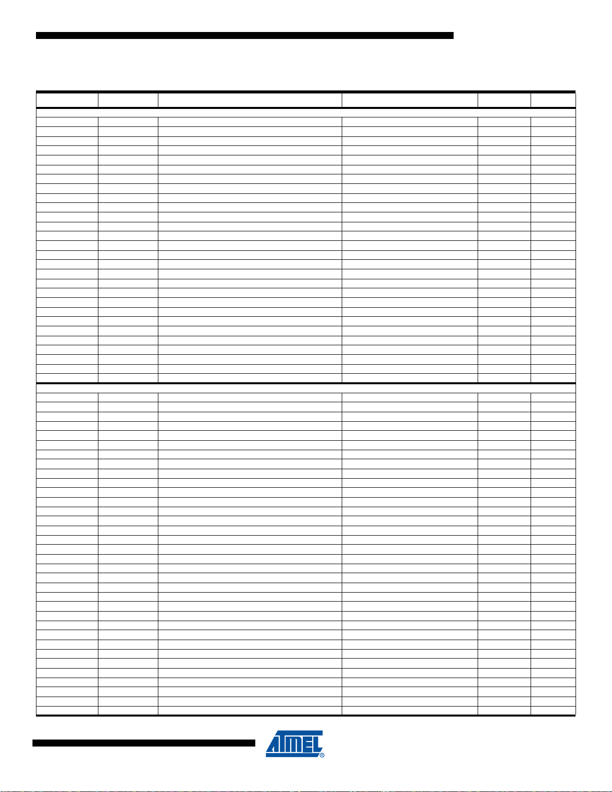
Packaging Information
44A
PIN 1
ATmega162/V
B
PIN 1 IDENTIFIER
e
E1 E
D1
D
C
0˚~7˚
A1
L
Notes: 1. This package conforms to JEDEC reference MS-026, Variation ACB.
2. Dimensions D1 and E1 do not include mold protrusion. Allowable
protrusion is 0.25 mm per side. Dimensions D1 and E1 are maximum
plastic body size dimensions including mold mismatch.
3. Lead coplanarity is 0.10 mm maximum.
A2 A
SYMBOL
COMMON DIMENSIONS
(Unit of Measure = mm)
MIN
A – – 1.20
A1 0.05 – 0.15
A2 0.95 1.00 1.05
D 11.75 12.00 12.25
D1 9.90 10.00 10.10 Note 2
E 11.75 12.00 12.25
E1 9.90 10.00 10.10 Note 2
B 0.30 – 0.45
C 0.09 – 0.20
L 0.45 – 0.75
e 0.80 TYP
NOM
MAX
NOTE
2513JS–AVR–08/07
2325 Orchard Parkway
R
San Jose, CA 95131
TITLE
44A, 44-lead, 10 x 10 mm Body Size, 1.0 mm Body Thickness,
0.8 mm Lead Pitch, Thin Profile Plastic Quad Flat Package (TQFP)
10/5/2001
DRAWING NO.
44A
REV.
B
15
Page 16

40P6
PIN
1
E1
A1
B
REF
E
B1
C
L
SEATING PLANE
A
D
e
0º ~ 15º
eB
Notes: 1. This package conforms to JEDEC reference MS-011, Variation AC.
2. Dimensions D and E1 do not include mold Flash or Protrusion.
Mold Flash or Protrusion shall not exceed 0.25 mm (0.010").
2325 Orchard Parkway
R
San Jose, CA 95131
TITLE
40P6, 40-lead (0.600"/15.24 mm Wide) Plastic Dual
Inline Package (PDIP)
COMMON DIMENSIONS
(Unit of Measure = mm)
SYMBOL
A – – 4.826
A1 0.381 – –
D 52.070 – 52.578 Note 2
E 15.240 – 15.875
E1 13.462 – 13.970 Note 2
B 0.356 – 0.559
B1 1.041 – 1.651
L 3.048 – 3.556
C 0.203 – 0.381
eB 15.494 – 17.526
e 2.540 TYP
MIN
NOM
MAX
DRAWING NO.
40P6
NOTE
09/28/01
REV.
B
16
ATmega162/V
2513JS–AVR–08/07
Page 17

44M1
ATmega162/V
D
Marked Pin# 1 ID
E
SEATING PLANE
TOP VIEW
K
L
D2
Pin #1 Corner
1
2
3
Option A
E2
Option B
K
b
e
Option C
BOTTOM VIEW
Note: JEDEC Standard MO-220, Fig. 1 (SAW Singulation) VKKD-3.
Pin #1
Tr iangle
Pin #1
Chamfer
(C 0.30)
Pin #1
Notch
(0.20 R)
A1
A3
A
SIDE VIEW
COMMON DIMENSIONS
(Unit of Measure = mm)
SYMBOL
A 0.80 0.90 1.00
A1 – 0.02 0.05
A3 0.25 REF
b 0.18 0.23 0.30
D
D2 5.00 5.20 5.40
E
E2 5.00 5.20 5.40
e 0.50 BSC
L 0.59 0.64 0.69
K 0.20 0.26 0.41
MIN
6.90 7.00 7.10
6.90 7.00 7.10
NOM
MAX
NOTE
2513JS–AVR–08/07
2325 Orchard Parkway
R
San Jose, CA 95131
TITLE
44M1, 44-pad, 7 x 7 x 1.0 mm Body, Lead Pitch 0.50 mm,
5.20 mm Exposed Pad, Micro Lead Frame Package (MLF)
DRAWING NO.
44M1
5/27/06
REV.
G
17
Page 18

Errata The revision letter in this section refers to the revision of the ATmega162 device.
ATmega162, all rev.
There are no errata for this revision of ATmega162. However, a proposal for solving problems
regarding the JTAG instruction IDCODE is presented below.
IDCODE masks data from TDI input
•
• Reading EEPROM by using ST or STS to set EERE bit triggers unexpected interrupt request
1. IDCODE masks data from TDI input
The public but optional JTAG instruction IDCODE is not implemented correctly according to
IEEE1149.1; a logic one is scanned into the shift register instead of the TDI input while shifting the Device ID Register. Hence, captured data from the preceding devices in the
boundary scan chain are lost and replaced by all-ones, and data to succeeding devices are
replaced by all-ones during Update-DR.
If ATmega162 is the only device in the scan chain, the problem is not visible.
Problem Fix / Workaround
Select the Device ID Register of the ATmega162 (Either by issuing the IDCODE instruction
or by entering the Test-Logic-Reset state of the TAP controller) to read out the contents of
its Device ID Register and possibly data from succeeding devices of the scan chain. Note
that data to succeeding devices cannot be entered during this scan, but data to preceding
devices can. Issue the BYPASS instruction to the ATmega162 to select its Bypass Register
while reading the Device ID Registers of preceding devices of the boundary scan chain.
Never read data from succeeding devices in the boundary scan chain or upload data to the
succeeding devices while the Device ID Register is selected for the ATmega162. Note that
the IDCODE instruction is the default instruction selected by the Test-Logic-Reset state of
the TAP-controller.
Alternative Problem Fix / Workaround
If the Device IDs of all devices in the boundary scan chain must be captured simultaneously
(for instance if blind interrogation is used), the boundary scan chain can be connected in
such way that the ATmega162 is the first device in the chain. Update-DR will still not work
for the succeeding devices in the boundary scan chain as long as IDCODE is present in the
JTAG Instruction Register, but the Device ID registered cannot be uploaded in any case.
18
2. Reading EEPROM by using ST or STS to set EERE bit triggers unexpected interrupt
request.
Reading EEPROM by using the ST or STS command to set the EERE bit in the EECR register triggers an unexpected EEPROM interrupt request.
Problem Fix / Workaround
Always use OUT or SBI to set EERE in EECR.
ATmega162/V
2513JS–AVR–08/07
Page 19

ATmega162/V
Datasheet Revision History
Changes from Rev. 2513I-04/07 to Rev. 2513J-08/07
Changes from Rev. 2513H-04/06 to Rev. 2513I-04/07
Please note that the referring page numbers in this section are referred to this document. The
referring revision in this section are referring to the document revision.
1. Updated “Features” on page 1.
2. Added “Data Retention” on page 7.
3. Updated “Errata” on page 18.
4. Updated “Version” on page 205.
5. Updated “C Code Example
6. Updated Figure 18 on page 35.
7. Updated “Clock Distribution” on page 35.
8. Updated “SPI Serial Programming Algorithm” on page 246.
9. Updated “Slave Mode” on page 162.
1. Updated “Using all 64KB Locations of External Memory” on page 34.
2. Updated “Bit 6 – ACBG: Analog Comparator Bandgap Select” on page 195.
(1)
” on page 172.
Changes from Rev. 2513G-03/05 to Rev. 2513H-04/06
Changes from Rev. 2513F-09/03 to Rev. 2513G-03/05
Changes from Rev. 2513D-04/03 to Rev. 2513E-09/03
3. Updated V
1. Added “Resources” on page 7.
2. Updated “Calibrated Internal RC Oscillator” on page 38.
3. Updated note for Table 19 on page 50.
4. Updated “Serial Peripheral Interface – SPI” on page 157.
1. MLF-package alternative changed to “Quad Flat No-Lead/Micro Lead Frame Package
QFN/MLF”.
2. Updated “Electrical Characteristics” on page 264
3. Updated “Ordering Information” on page 14
1. Removed “Preliminary” from the datasheet.
2. Added note on Figure 1 on page 2.
3. Renamed and updated “On-chip Debug System” to “JTAG Interface and On-chip
Debug System” on page 46.
conditions in“DC Characteristics” on page 264.
OH
2513JS–AVR–08/07
4. Updated Table 18 on page 48 and Table 19 on page 50.
19
Page 20

5. Updated “Test Access Port – TAP” on page 197 regarding JTAGEN.
6. Updated description for the JTD bit on page 207.
7. Added note on JTAGEN in Table 99 on page 233.
8. Updated Absolute Maximum Ratings* and DC Characteristics in “Electrical Character-
istics” on page 264.
9. Added a proposal for solving problems regarding the JTAG instruction IDCODE in
“Errata” on page 18.
Changes from Rev. 2513C-09/02 to Rev. 2513D-04/03
1. Updated the “Ordering Information” on page 14 and “Packaging Information” on page
15.
2. Updated “Features” on page 1.
3. Added characterization plots under “ATmega162 Typical Characteristics” on page
275.
4. Added Chip Erase as a first step under “Programming the Flash” on page 260 and
“Programming the EEPROM” on page 262.
5. Changed CAL7, the highest bit in the OSCCAL Register, to a reserved bit on page 39
and in “Register Summary” on page 8.
6. Changed CPCE to CLKPCE on page 41.
7. Corrected code examples on page 55.
8. Corrected OCn waveforms in Figure 52 on page 120.
9. Various minor Timer1 corrections.
10. Added note under “Filling the Temporary Buffer (Page Loading)” on page 224 about
writing to the EEPROM during an SPM Page Load.
20
11. Added section “EEPROM Write During Power-down Sleep Mode” on page 24.
12. Added information about PWM symmetry for Timer0 on page 98 and Timer2 on page
147.
13. Updated Table 18 on page 48, Table 20 on page 50, Table 36 on page 77, Table 83 on
page 205, Table 109 on page 247, Table 112 on page 267, and Table 113 on page 268.
14. Added Figures for “Absolute Maximum Frequency as a function of VCC, ATmega162”
on page 266.
15. Updated Figure 29 on page 64, Figure 32 on page 68, and Figure 88 on page 210.
16. Removed Table 114, “External RC Oscillator, Typical Frequencies
17. Updated “Electrical Characteristics” on page 264.
ATmega162/V
(1)
,” on page 265.
2513JS–AVR–08/07
Page 21

ATmega162/V
Changes from Rev. 2513B-09/02 to Rev. 2513C-09/02
Changes from Rev. 2513A-05/02 to Rev. 2513B-09/02
1. Changed the Endurance on the Flash to 10,000 Write/Erase Cycles.
1. Added information for ATmega162U.
Information about ATmega162U included in “Features” on page 1, Table 19,
“BODLEVEL Fuse Coding,” on page 50, and “Ordering Information” on page 14.
2513JS–AVR–08/07
21
Page 22

Headquarters International
Atmel Corporation
2325 Orchard Parkway
San Jose, CA 95131
USA
Tel: 1(408) 441-0311
Fax: 1(408) 487-2600
Atmel Asia
Room 1219
Chinachem Golden Plaza
77 Mody Road Tsimshatsui
East Kowloon
Hong Kong
Tel: (852) 2721-9778
Fax: (852) 2722-1369
Product Contact
Web Site
www.atmel.com
Literature Requests
www.atmel.com/literature
Atmel Europe
Le Krebs
8, Rue Jean-Pierre Timbaud
BP 309
78054 Saint-Quentin-enYvelines Cedex
France
Tel: (33) 1-30-60-70-00
Fax: (33) 1-30-60-71-11
Technical Support
avr@atmel.com
Atmel Japan
9F, Tonetsu Shinkawa Bldg.
1-24-8 Shinkawa
Chuo-ku, Tokyo 104-0033
Japan
Tel: (81) 3-3523-3551
Fax: (81) 3-3523-7581
Sales Contact
www.atmel.com/contacts
Disclaimer: The information in this document is provided in connection with Atmel products. No license, express or implied, by estoppel or otherwise, to any
intellectual property right is granted by this document or in connection with the sale of Atmel products. EXCEPT AS SET FORTH IN ATMEL’S TERMS AND CONDI-
TIONS OF SALE LOCATED ON ATMEL’S WEB SITE, ATMEL ASSUMES NO LIABILITY WHATSOEVER AND DISCLAIMS ANY EXPRESS, IMPLIED OR STATUTORY
WARRANTY RELATING TO ITS PRODUCTS INCLUDING, BUT NOT LIMITED TO, THE IMPLIED WARRANTY OF MERCHANTABILITY, FITNESS FOR A PARTICULAR
PURPOSE, OR NON-INFRINGEMENT. IN NO EVENT SHALL ATMEL BE LIABLE FOR ANY DIRECT, INDIRECT, CONSEQUENTIAL, PUNITIVE, SPECIAL OR INCIDENTAL DAMAGES (INCLUDING, WITHOUT LIMITATION, DAMAGES FOR LOSS OF PROFITS, BUSINESS INTERRUPTION, OR LOSS OF INFORMATION) ARISING OUT OF
THE USE OR INABILITY TO USE THIS DOCUMENT, EVEN IF ATMEL HAS BEEN ADVISED OF THE POSSIBILITY OF SUCH DAMAGES. Atmel makes no
representations or warranties with respect to the accuracy or completeness of the contents of this document and reserves the right to make changes to specifications
and product descriptions at any time without notice. Atmel does not make any commitment to update the information contained herein. Unless specifically provided
otherwise, Atmel products are not suitable for, and shall not be used in, automotive applications. Atmel’s products are not intended, authorized, or warranted for use
as components in applications intended to support or sustain life.
© 2007 Atmel Corporation. All rights reserved. Atmel®, logo and combinations thereof, AVR® and others are registered trademarks or trade-
marks of Atmel Corporation or its subsidiaries. Other terms and product names may be trademarks of others.
2513JS–AVR–08/07
 Loading...