


BDTIC www.bdtic.com/ATMEL
Features
• Incorporates the ARM926EJ-S
– DSP Instruction Extensions, Jazelle
– 16 Kbyte Data Cache, 16 Kbyte Instruction Cache, Write Buffer
– 220 MIPS at 200 MHz
– Memory Management Unit
– EmbeddedICE
– Mid-level Implementation Embedded Trace Macrocell
™
, Debug Communication Channel Support
• Bus Matrix
– Nine 32-bit-layer Matrix, Allowing a Total of 28.8 Gbps of On-chip Bus Bandwidth
– Boot Mode Select Option, Remap Command
• Embedded Memories
– One 128 Kbyte Internal ROM, Single-cycle Access at Maximum Bus Matrix Speed
– One 80 Kbyte Internal SRAM, Single-cycle Access at Maximum Processor or Bus
Matrix Speed
– One 16 Kbyte Internal SRAM, Single-cycle Access at Maximum Bus Matrix Speed
• Dual External Bus Interface (EBI0 and EBI1)
– EBI0 Supports SDRAM, Static Memory, ECC-enabled NAND Flash and
CompactFlash
– EBI1 Supports SDRAM, Static Memory and ECC-enabled NAND Flash
®
• DMA Controller (DMAC)
– Acts as one Bus Matrix Master
– Embeds 2 Unidirectional Channels with Programmable Priority, Address
Generation, Channel Buffering and Control
• Twenty Peripheral DMA Controller Channels (PDC)
• LCD Controller
– Supports Passive or Active Displays
– Up to 24 bits per Pixel in TFT Mode, Up to 16 bits per Pixel in STN Color Mode
– Up to 16M Colors in TFT Mode, Resolution Up to 2048x2048, Supports Virtual
Screen Buffers
• Two D Graphics Accelerator
– Line Draw, Block Transfer, Clipping, Commands Queuing
• Image Sensor Interface
– ITU-R BT. 601/656 External Interface, Programmable Frame Capture Rate
– 12-bit Data Interface for Support of High Sensibility Sensors
– SAV and EAV Synchronization, Preview Path with Scaler, YCbCr Format
• USB 2.0 Full Speed (12 Mbits per second) Host Double Port
– Dual On-chip Transceivers
– Integrated FIFOs and Dedicated DMA Channels
• USB 2.0 Full Speed (12 Mbits per second) Device Port
– On-chip Transceiver, 2,432-byte Configurable Integrated DPRAM
• Ethernet MAC 10/100 Base-T
– Media Independent Interface or Reduced Media Independent Interface
– 28-byte FIFOs and Dedicated DMA Channels for Receive and Transmit
• Fully-featured System Controller, including
– Reset Controller, Shutdown Controller
– Twenty 32-bit Battery Backup Registers for a Total of 80 Bytes
– Clock Generator and Power Management Controller
– Advanced Interrupt Controller and Debug Unit
™
ARM® Thumb® Processor
®
Technology for Java® Acceleration
™
AT91 ARM
Thumb
Microcontrollers
AT91SAM9263
Preliminary
6249G–ATARM–06-Jan-09

– Periodic Interval Timer, Watchdog Timer and Double Real-time Timer
• Reset Controller (RSTC)
– Based on Two Power-on Reset Cells, Reset Source Identification and Reset Output Control
• Shutdown Controller (SHDWC)
– Programmable Shutdown Pin Control and Wake-up Circuitry
• Clock Generator (CKGR)
– 32768Hz Low-power Oscillator on Battery Backup Power Supply, Providing a Permanent Slow Clock
– 3 to 20 MHz On-chip Oscillator and Two Up to 240 MHz PLLs
• Power Management Controller (PMC)
– Very Slow Clock Operating Mode, Software Programmable Power Optimization Capabilities
– Four Programmable External Clock Signals
• Advanced Interrupt Controller (AIC)
– Individually Maskable, Eight-level Priority, Vectored Interrupt Sources
– Two External Interrupt Sources and One Fast Interrupt Source, Spurious Interrupt Protected
• Debug Unit (DBGU)
– 2-wire UART and Support for Debug Communication Channel, Programmable ICE Access Prevention
– Mode for General Purpose Two-wire UART Serial Communication
• Periodic Interval Timer (PIT)
– 20-bit Interval Timer plus 12-bit Interval Counter
• Watchdog Timer (WDT)
– Key-protected, Programmable Only Once, Windowed 16-bit Counter Running at Slow Clock
• Two Real-time Timers (RTT)
– 32-bit Free-running Backup Counter Running at Slow Clock with 16-bit Prescaler
• Five 32-bit Parallel Input/Output Controllers (PIOA, PIOB, PIOC, PIOD and PIOE)
– 160 Programmable I/O Lines Multiplexed with Up to Two Peripheral I/Os
– Input Change Interrupt Capability on Each I/O Line
– Individually Programmable Open-drain, Pull-up Resistor and Synchronous Output
• One Part 2.0A and Part 2.0B-compliant CAN Controller
– 16 Fully-programmable Message Object Mailboxes, 16-bit Time Stamp Counter
• Two Multimedia Card Interface (MCI)
™
– SDCard/SDIO and MultiMediaCard
– Automatic Protocol Control and Fast Automatic Data Transfers with PDC
– Two SDCard Slots Support on eAch Controller
Compliant
• Two Synchronous Serial Controllers (SSC)
– Independent Clock and Frame Sync Signals for Each Receiver and Transmitter
– I²S Analog Interface Support, Time Division Multiplex Support
– High-speed Continuous Data Stream Capabilities with 32-bit Data Transfer
• One AC97 Controller (AC97C)
– 6-channel Single AC97 Analog Front End Interface, Slot Assigner
• Three Universal Synchronous/Asynchronous Receiver Transmitters (USART)
®
– Individual Baud Rate Generator, IrDA
– Support for ISO7816 T0/T1 Smart Card, Hardware Handshaking, RS485 Support
Infrared Modulation/Demodulation, Manchester Encoding/Decoding
• Two Master/Slave Serial Peripheral Interface (SPI)
– 8- to 16-bit Programmable Data Length, Four External Peripheral Chip Selects
• One Three-channel 16-bit Timer/Counters (TC)
– Three External Clock Inputs, Two Multi-purpose I/O Pins per Channel
– Double PWM Generation, Capture/Waveform Mode, Up/Down Capability
• One Four-channel 16-bit PWM Controller (PWMC)
• One Two-wire Interface (TWI)
®
– Master Mode Support, All Two-wire Atmel
EEPROMs Supported
2
AT91SAM9263 Preliminary
6249G–ATARM–06-Jan-09

AT91SAM9263 Preliminary
®
• IEEE
• Required Power Supplies
• Available in a 324-ball TFBGA Green Package
1. Description
The AT91SAM9263 32-bit microcontroller, based on the ARM926EJ-S processor, is architectured on a 9-layer matrix,
allowing a maximum internal bandwidth of nine 32-bit buses. It also features two independent external memory buses,
EBI0 and EBI1, capable of interfacing with a wide range of memory devices and an IDE hard disk. Two external buses prevent bottlenecks, thus guaranteeing maximum performance.
The AT91SAM9263 embeds an LCD Controller supported by a Two D Graphics Controller and a 2-channel DMA Controller, and one Image Sensor Interface. It also integrates several standard peripherals, such as USART, SPI, TWI, Timer
Counters, PWM Generators, Multimedia Card interface and one CAN Controller.
When coupled with an external GPS engine, the AT91SAM9263 provides the ideal solution for navigation systems.
1149.1 JTAG Boundary Scan on All Digital Pins
– 1.08V to 1.32V for VDDCORE and VDDBU
– 3.0V to 3.6V for VDDOSC and VDDPLL
– 2.7V to 3.6V for VDDIOP0 (Peripheral I/Os)
– 1.65V to 3.6V for VDDIOP1 (Peripheral I/Os)
– Programmable 1.65V to 1.95V or 3.0V to 3.6V for VDDIOM0/VDDIOM1 (Memory I/Os)
6249G–ATARM–06-Jan-09
3
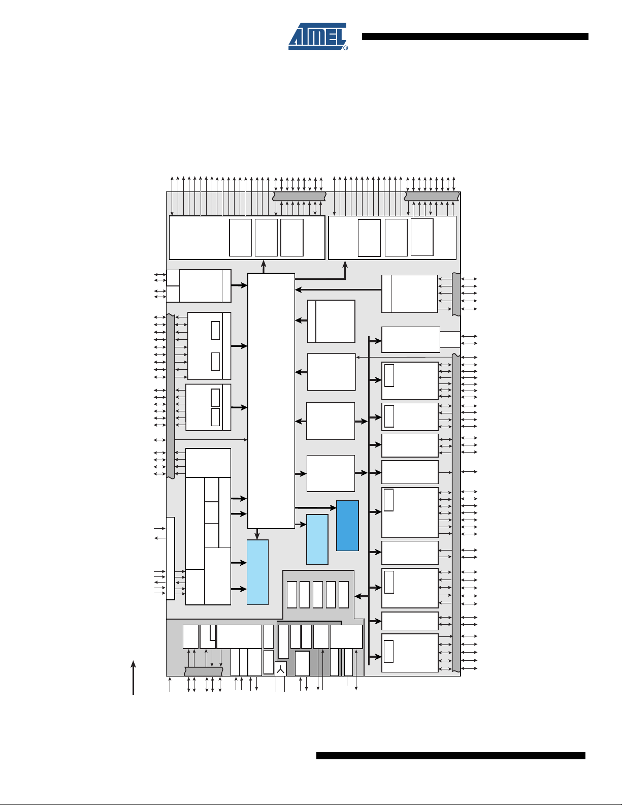
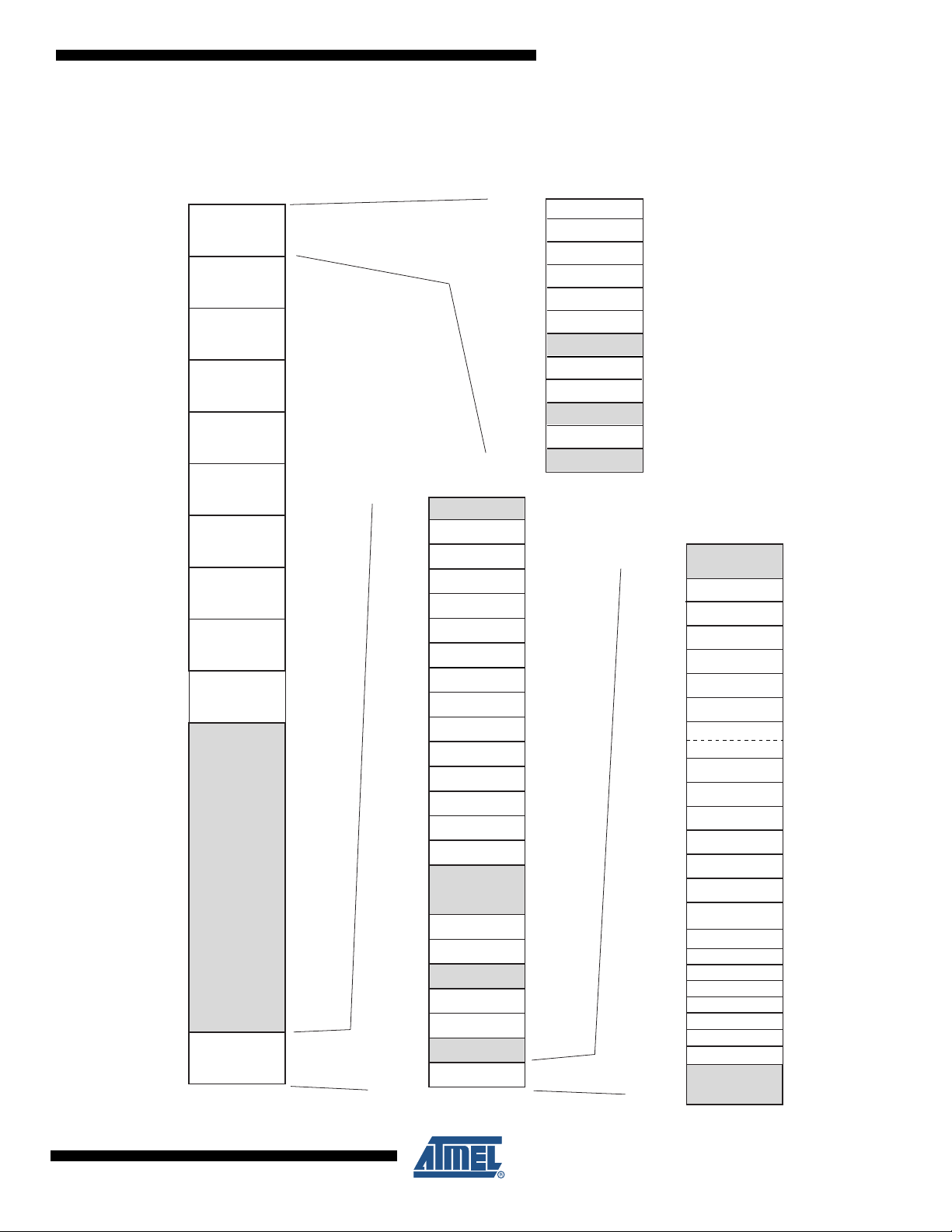
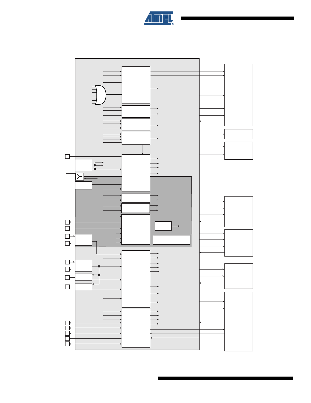
2. AT91SAM9263 Block Diagram
ARM926EJ-S Processor
JTAG Boundary Scan
In-Circuit
Emulator
AIC
Fast SRAM
80 Kbytes
SSC0
SSC1
D0-D15
A0/NBS0
A2-A15, A18-A20
A16/BA0
A17/BA1
NCS0
NCS1/SDCS
NRD
NWR0/NWE
NWR1/NBS1
NWR3/NBS3
SDCK, SDCKE
RAS, CAS
SDWE, SDA10
FIQ
IRQ0-IRQ1
PLLRCB
PLLRCA
DRXD
DTXD
LCD
Controller
ICache
16K bytes
DCache
16K bytes
MMU
DMA
APB
ROM
128 Kbytes
Peripheral
Bridge
20-channel
Peripheral
DMA
ETM
TCLK
PDC
PLLA
ITCM DTCM
Bus Interface
TCM Interface
A1/NBS2/NWR2
TST
PCK0-PCK3
System
Controller
VDDBU
SHDN
WKUP
XIN
TSYNC
TPS0-TPS2
TPK0-TPK15
TDI
TDO
TMS
TCK
JTAGSEL
ID
FIFO
LUT
LCDD0-LCDD23
LCDVSYNC
LCDHSYNC
LCDDOTCK
LCDDEN
LCDCC
EBI1
D0-D15
A0/NBS0
A2-A15/A18-A20
NCS0
NCS1/SDCS
NRD
NWR0/NWE
NWR1/NBS1
Static
Memory
Controller
NCS2/NANDCS
A1/NWR2
NWAIT
DMARQ0_DMARQ3
2D
Graphics
Controller
NRST
TK0-TK1
TF0-TF1
TD0-TD1
RD0-RD1
RF0-RF1
RK0-RK1
TC0
TC1
TC2
TCLK0-TCLK2
TIOA0-TIOA2
TIOB0-TIOB2
NPCS2
NPCS1
SPCK
MOSI
MISO
NPCS0
SPI0
SPI1
PDC
NPCS3
USART0
USART1
USART2
RTS0-RTS2
SCK0-SCK2
TXD0-TXD2
RDX0-RDX2
CTS0-CTS2
PDC
TWI
TWCK
TWD
MCI0
MCI1
PDC
CK
DA0-DA3
CDA
DB0-DB3
CDB
EBI0_
NANDOE, NANDWE
EBI1_
PMC
PLLB
OSC
XOUT
PITWDT
RTT0
OSC
XIN32
XOUT32
SHDWC
POR
RSTC
POR
DBGU
9-layer Bus Matrix
2-channel
DMA
SLAVEMASTER
PDC
BMS
20GPREG
A23-A24
NCS5/CFCS1
A25/CFRNW
NCS4/CFCS0
D16-D31
NWAIT
CFCE1-CFCE2
EBI0
Static
Memory
Controller
CompactFlash
NAND Flash
SDRAM
Controller
NCS2
NCS3/NANDCS
PWMC
PWM0-PWM3
CAN
CANRX
CANTX
ETXCK-ERXCK-EREFCK
ETXEN-ETXER
ECRS-ECOL
ERXER-ERXDV
ERX0-ERX3
ETX0-ETX3
EMDC
EMDIO
EF100
10/100 Ethernet
MAC
FIFO
DMA
FIFO
PIOA
PIOB
PIOD
PIOC
Image
Sensor
Interface
ISI_PCK
ISI_D0-ISI_D11
ISI_HSYNC
ISI_VSYNC
ISI_MCK
VDDCORE
DMA
PIOE
SDCKE
RAS, CAS
SDWE, SDA10
SDRAM
Controller
D16-D31
SRAM
16 Kbytes
RTCK
ECC
Controller
DMA
A16/BA0
A17/BA1
ECC
Controller
NAND Flash
NANDOE, NANDWE
NWR3/NBS3
AC97C
PDC
AC97CK
AC97FS
AC97RX
AC97TX
VDDCORE
USB
OHCI
DMA
USB
Device
Por t
Transc.
DDP
DDM
SPI0_, SPI1_MCI0_, MCI_1
RTT1
Transc.
Transc.
HDPA
HDMA
HDPB
HDMB
SDCK
NTRST
A21/NANDALE
A22/NANDCLE
A21/NANDALE
A22/NANDCLE
Figure 2-1. AT91SAM9263 Block Diagram
4
AT91SAM9263 Preliminary
6249G–ATARM–06-Jan-09
AT91SAM9263 Preliminary
3. Signal Description
Table 3-1 gives details on the signal name classified by peripheral.
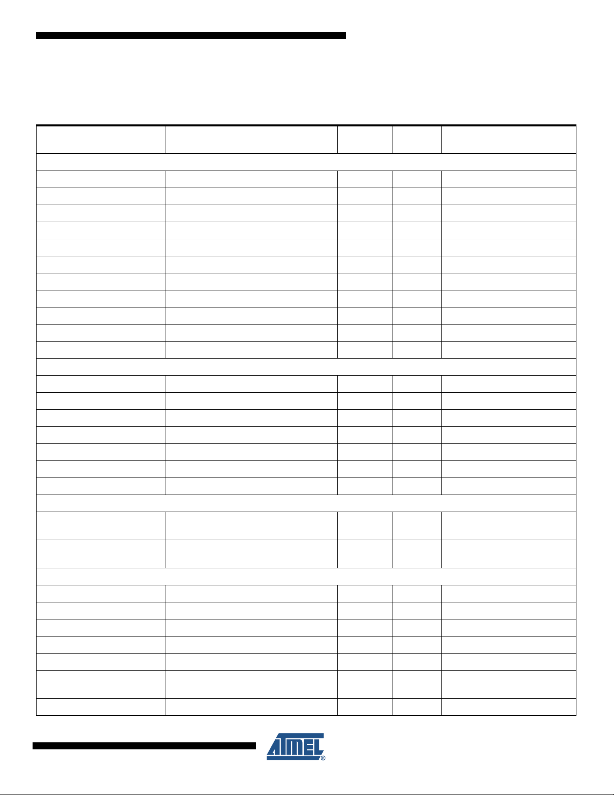
Table 3-1. Signal Description List
Active
Signal Name Function Type
Power Supplies
VDDIOM0 EBI0 I/O Lines Power Supply Power 1.65V to 3.6V
VDDIOM1 EBI1 I/O Lines Power Supply Power 1.65V to 3.6V
VDDIOP0 Peripherals I/O Lines Power Supply Power 2.7V to 3.6V
VDDIOP1 Peripherals I/O Lines Power Supply Power 1.65V to 3.6V
VDDBU Backup I/O Lines Power Supply Power 1.08V to 1.32V
VDDPLL PLL Power Supply Power 3.0V to 3.6V
VDDOSC Oscillator Power Supply Power 3.0V to 3.6V
VDDCORE Core Chip Power Supply Power 1.08V to 1.32V
GND Ground Ground
GNDPLL PLL Ground Ground
Level Comments
GNDBU Backup Ground Ground
Clocks, Oscillators and PLLs
XIN Main Oscillator Input Input
XOUT Main Oscillator Output Output
XIN32 Slow Clock Oscillator Input Input
XOUT32 Slow Clock Oscillator Output Output
PLLRCA PLL A Filter Input
PLLRCB PLL B Filter Input
PCK0 - PCK3 Programmable Clock Output Output
Shutdown, Wakeup Logic
SHDN Shutdown Control Output
WKUP Wake-up Input Input
ICE and JTAG
NTRST Test Reset Signal Input Low Pull-up resistor
TCK Test Clock Input No pull-up resistor
TDI Test Data In Input No pull-up resistor
Driven at 0V only. Do not tie
over VDDBU.
Accepts between 0V and
VDDBU.
TDO Test Data Out Output
TMS Test Mode Select Input No pull-up resistor
JTAGSEL JTAG Selection Input
RTCK Return Test Clock Output
6249G–ATARM–06-Jan-09
Pull-down resistor. Accepts
between 0V and VDDBU.
5

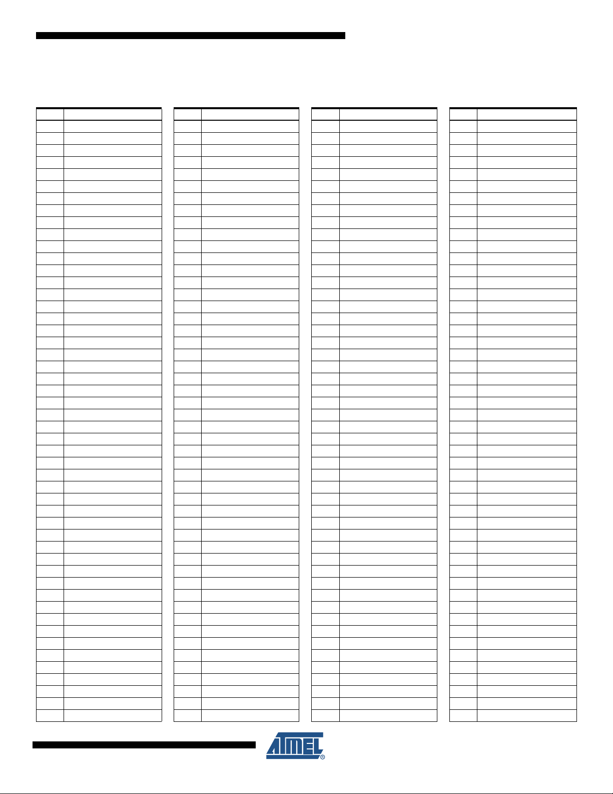
Table 3-1. Signal Description List (Continued)
Active
Signal Name Function Type
Embedded Trace Module - ETM
TSYNC Trace Synchronization Signal Output
TCLK Trace Clock Output
TPS0 - TPS2 Trace ARM Pipeline Status Output
TPK0 - TPK15 Trace Packet Port Output
Reset/Test
NRST Microcontroller Reset I/O Low Pull-up resistor
TST Test Mode Select Input Pull-down resistor
BMS Boot Mode Select Input
Debug Unit - DBGU
DRXD Debug Receive Data Input
DTXD Debug Transmit Data Output
Advanced Interrupt Controller - AIC
IRQ0 - IRQ1 External Interrupt Inputs Input
FIQ Fast Interrupt Input Input
Level Comments
PIO Controller - PIOA - PIOB - PIOC - PIOD - PIOE
PA0 - PA31 Parallel IO Controller A I/O Pulled-up input at reset
PB0 - PB31 Parallel IO Controller B I/O Pulled-up input at reset
PC0 - PC31 Parallel IO Controller C I/O Pulled-up input at reset
PD0 - PD31 Parallel IO Controller D I/O Pulled-up input at reset
PE0 - PE31 Parallel IO Controller E I/O Pulled-up input at reset
Direct Memory Access Controller - DMA
DMARQ0-DMARQ3 DMA Requests Input
External Bus Interface - EBI0 - EBI1
EBIx_D0 - EBIx_D31 Data Bus I/O Pulled-up input at reset
EBIx_A0 - EBIx_A25 Address Bus Output 0 at reset
EBIx_NWAIT External Wait Signal Input Low
Static Memory Controller - SMC
EBI0_NCS0 - EBI0_NCS5,
EBI1_NCS0 - EBI1_NCS2
EBIx_NWR0 -EBIx_NWR3 Write Signal Output Low
EBIx_NRD Read Signal Output Low
EBIx_NWE Write Enable Output Low
EBIx_NBS0 - EBIx_NBS3 Byte Mask Signal Output Low
Chip Select Lines Output Low
6
AT91SAM9263 Preliminary
6249G–ATARM–06-Jan-09

AT91SAM9263 Preliminary
Table 3-1. Signal Description List (Continued)
Active
Signal Name Function Type
CompactFlash Support
EBI0_CFCE1 - EBI0_CFCE2 CompactFlash Chip Enable Output Low
EBI0_CFOE CompactFlash Output Enable Output Low
EBI0_CFWE CompactFlash Write Enable Output Low
EBI0_CFIOR CompactFlash IO Read Output Low
EBI0_CFIOW CompactFlash IO Write Output Low
EBI0_CFRNW CompactFlash Read Not Write Output
EBI0_CFCS0 - EBI0_CFCS1 CompactFlash Chip Select Lines Output Low
NAND Flash Support
EBIx_NANDCS NAND Flash Chip Select Output Low
EBIx_NANDOE NAND Flash Output Enable Output Low
EBIx_NANDWE NAND Flash Write Enable Output Low
SDRAM Controller
EBIx_SDCK SDRAM Clock Output
EBIx_SDCKE SDRAM Clock Enable Output High
Level Comments
EBIx_SDCS SDRAM Controller Chip Select Output Low
EBIx_BA0 - EBIx_BA1 Bank Select Output
EBIx_SDWE SDRAM Write Enable Output Low
EBIx_RAS - EBIx_CAS Row and Column Signal Output Low
EBIx_SDA10 SDRAM Address 10 Line Output
Multimedia Card Interface
MCIx_CK Multimedia Card Clock Output
MCIx_CDA Multimedia Card Slot A Command I/O
MCIx_CDB Multimedia Card Slot B Command I/O
MCIx_DA0 - MCIx_DA3 Multimedia Card Slot A Data I/O
MCIx_DB0 - MCIx_DB3 Multimedia Card Slot B Data I/O
Universal Synchronous Asynchronous Receiver Transmitter USART
SCKx USARTx Serial Clock I/O
TXDx USARTx Transmit Data I/O
RXDx USARTx Receive Data Input
RTSx USARTx Request To Send Output
CTSx USARTx Clear To Send Input
Synchronous Serial Controller SSC
TDx SSCx Transmit Data Output
RDx SSCx Receive Data Input
6249G–ATARM–06-Jan-09
7

Table 3-1. Signal Description List (Continued)
Signal Name Function Type
TKx SSCx Transmit Clock I/O
RKx SSCx Receive Clock I/O
TFx SSCx Transmit Frame Sync I/O
RFx SSCx Receive Frame Sync I/O
AC97 Controller - AC97C
AC97RX AC97 Receive Signal Input
AC97TX AC97 Transmit Signal Output
AC97FS AC97 Frame Synchronization Signal Output
AC97CK AC97 Clock signal Input
Timer/Counter - TC
TCLKx TC Channel x External Clock Input Input
TIOAx TC Channel x I/O Line A I/O
TIOBx TC Channel x I/O Line B I/O
Pulse Width Modulation Controller- PWMC
PWMx Pulse Width Modulation Output Output
Active
Level Comments
Serial Peripheral Interface - SPI
SPIx_MISO Master In Slave Out I/O
SPIx_MOSI Master Out Slave In I/O
SPIx_SPCK SPI Serial Clock I/O
SPIx_NPCS0 SPI Peripheral Chip Select 0 I/O Low
SPIx_NPCS1 - SPIx_NPCS3 SPI Peripheral Chip Select Output Low
Two-Wire Interface
TWD Two-wire Serial Data I/O
TWCK Two-wire Serial Clock I/O
CAN Controllers
CANRX CAN Input Input
CANTX CAN Output Output
LCD Controller - LCDC
LCDD0 - LCDD23 LCD Data Bus Output
LCDVSYNC LCD Vertical Synchronization Output
LCDHSYNC LCD Horizontal Synchronization Output
LCDDOTCK LCD Dot Clock Output
LCDDEN LCD Data Enable Output
LCDCC LCD Contrast Control Output
8
AT91SAM9263 Preliminary
6249G–ATARM–06-Jan-09

AT91SAM9263 Preliminary
Table 3-1. Signal Description List (Continued)
Active
Signal Name Function Type
Ethernet 10/100
ETXCK Transmit Clock or Reference Clock Input MII only, REFCK in RMII
ERXCK Receive Clock Input MII only
ETXEN Transmit Enable Output
ETX0-ETX3 Transmit Data Output ETX0-ETX1 only in RMII
ETXER Transmit Coding Error Output MII only
ERXDV Receive Data Valid Input RXDV in MII, CRSDV in RMII
ERX0-ERX3 Receive Data Input ERX0-ERX1 only in RMII
ERXER Receive Error Input
ECRS Carrier Sense and Data Valid Input MII only
ECOL Collision Detect Input MII only
EMDC Management Data Clock Output
EMDIO Management Data Input/Output I/O
EF100 Force 100Mbit/sec. Output High RMII only
USB Device Port
Level Comments
DDM USB Device Port Data - Analog
DDP USB Device Port Data + Analog
USB Host Port
HDPA USB Host Port A Data + Analog
HDMA USB Host Port A Data - Analog
HDPB USB Host Port B Data + Analog
HDMB USB Host Port B Data - Analog
Image Sensor Interface - ISI
ISI_D0-ISI_D11 Image Sensor Data Input
ISI_MCK Image Sensor Reference Clock Output Provided by PCK3
ISI_HSYNC Image Sensor Horizontal Synchro Input
ISI_VSYNC Image Sensor Vertical Synchro Input
ISI_PCK Image Sensor Data Clock Input
6249G–ATARM–06-Jan-09
9

4. Package and Pinout
The AT91SAM9263 is available in a 324-ball TFBGA Green package, 15 x 15 mm, 0.8mm ball
pitch.
4.1 324-ball TFBGA Package Outline
Figure 4-1 shows the orientation of the 324-ball TFBGA package.
A detailed mechanical description is given in the section “AT91SAM9263 Mechanical Characteristics” in the product datasheet.
Figure 4-1. 324-ball TFBGA Pinout (Top View)
10
AT91SAM9263 Preliminary
6249G–ATARM–06-Jan-09
AT91SAM9263 Preliminary
4.2 324-ball TFBGA Package Pinout
Table 4-1. AT91SAM9263 Pinout for 324-ball TFBGA Package
Pin Signal Name Pin Signal Name Pin Signal Name Pin Signal Name
A1 EBI0_D2 E10 PC31 K1 PE6 P10 EBI1_NCS0
A2 EBI0_SDCKE E11 PC22 K2 PD28 P11 EBI1_NWE_NWR0
A3 EBI0_NWE_NWR0 E12 PC15 K3 PE0 P12 EBI1_D4
A4 EBI0_NCS1_SDCS E13 PC11 K4 PE1 P13 EBI1_D10
A5 EBI0_A19 E14 PC4 K5 PD27 P14 PA3
A6 EBI0_A11 E15 PB30 K6 PD31 P15 PA2
A7 EBI0_A10 E16 PC0 K7 PD29 P16 PE28
A8 EBI0_A5 E17 PB31 K8 PD25 P17 TDI
A9 EBI0_A1_NBS2_NWR2 E18 HDPA K9 GND P18 PLLRCB
A10 PD4 F1 PD7 K10 VDDIOM0 R1 XOUT32
A11 PC30 F2 EBI0_D13 K11 GND R2 TST
A12 PC26 F3 EBI0_D9 K12 VDDIOM0 R3 PA18
A13 PC24 F4 EBI0_D11 K13 PB3/BMS R4 PA25
A14 PC19 F5 EBI0_D12 K14 PA14 R5 PA30
A15 PC12 F6 EBI0_NCS0 K15 PA15 R6 EBI1_A2
A16 VDDCORE F7 EBI0_A16_BA0 K16 PB1 R7 EBI1_A14
A17 VDDIOP0 F8 EBI0_A12 K17 PB0 R8 EBI1_A13
A18 DDP F9 EBI0_A6 K18 PB2 R9 EBI1_A17_BA1
B1 EBI0_D4 F10 PD3 L1 PE10 R10 EBI1_D1
B2 EBI0_NANDOE F11 PC27 L2 PE4 R11 EBI1_D8
B3 EBI0_CAS F12 PC18 L3 PE9 R12 EBI1_D12
B4 EBI0_RAS F13 PC13 L4 PE7 R13 EBI1_D15
B5 EBI0_NBS3_NWR3 F14 PB26 L5 PE5 R14 PE26
B6 EBI0_A22 F15 PB25 L6 PE2 R15 EBI1_SDCK
B7 EBI0_A15 F16 PB29 L7 PE3 R16 PE30
B8 EBI0_A7 F17 PB27 L8 VDDIOP1 R17 TCK
B9 EBI0_A4 F18 HDMA L9 VDDIOM1 R18 XOUT
B10 PD0 G1 PD17 L10 VDDIOM0 T1 VDDOSC
B11 PC28 G2 PD12 L11 VDDIOP0 T2 VDDIOM1
B12 PC21 G3 PD6 L12 GNDBU T3 PA19
B13 PC17 G4 EBI0_D14 L13 PA13 T4 PA21
B14 PC9 G5 PD5 L14 PB4 T5 PA26
B15 PC7 G6 PD8 L15 PA9 T6 PA31
B16 PC5 G7 PD10 L16 PA12 T7 EBI1_A7
B17 PB16 G8 GND L17 PA10 T8 EBI1_A12
B18 DDM G9 NC
C1 EBI0_D6 G10 GND M1 PE18 T10 EBI1_D0
C2 EBI0_D0 G11 GND M2 PE14 T11 EBI1_D7
C3 EBI0_NANDWE G12 GND M3 PE15 T12 EBI1_D14
C4 EBI0_SDWE G13 PB21 M4 PE11 T13 PE23
C5 EBI0_SDCK G14 PB20 M5 PE13 T14 PE25
C6 EBI0_A21 G15 PB23 M6 PE12 T15 PE29
C7 EBI0_A13 G16 PB28 M7 PE8 T16 PE31
C8 EBI0_A8 G17 PB22 M8 VDDBU T17 GNDPLL
C9 EBI0_A3 G18 PB18 M9 EBI1_A21 T18 XIN
C10 PD2 H1 PD24 M10 VDDIOM1 U1 PA17
C11 PC29 H2 PD13 M11 GND U2 PA20
C12 PC23 H3 PD15 M12 GND U3 PA23
C13 PC14 H4 PD9 M13 VDDIOM1 U4 PA24
C14 PC8 H5 PD11 M14 PA6 U5 PA28
(1)
L18 PA11 T9 EBI1_A18
6249G–ATARM–06-Jan-09
11
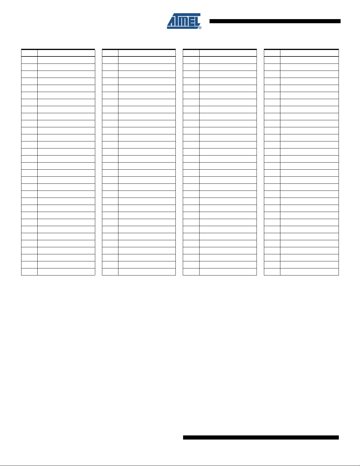
Table 4-1. AT91SAM9263 Pinout for 324-ball TFBGA Package (Continued)
Pin Signal Name Pin Signal Name Pin Signal Name Pin Signal Name
C15 PC3 H6 PD14 M15 PA4 U6 EBI1_A0_NBS0
C16 GND H7 PD16 M16 PA7 U7 EBI1_A5
C17 VDDIOP0 H8 VDDIOM0 M17 PA5 U8 EBI1_A10
C18 HDPB H9 GND M18 PA8 U9 EBI1_A16_BA0
D1 EBI0_D10 H10 VDDCORE N1 NC U10 EBI1_NRD
D2 EBI0_D3 H11 GND N2 NC U11 EBI1_D3
D3 NC
D4 EBI0_D1 H13 PB17 N4 NC
D5 EBI0_A20 H14 PB15 N5 PE17 U14 PE27
D6 EBI0_A17_BA1 H15 PB13 N6 PE16 U15 RTCK
D7 EBI0_A18 H16 PB24 N7 EBI1_A6 U16 NTRST
D8 EBI0_A9 H17 PB14 N8 EBI1_A11 U17 VDDPLLA
D9 EBI0_A2 H18 PB12 N9 EBI1_A22 U18 PLLRCA
D10 PD1 J1 PD30 N10 EBI1_D2 V1 VDDCORE
D11 PC25 J2 PD26 N11 EBI1_D6 V2 PA22
D12 PC20 J3 PD22 N12 EBI1_D9 V3 PA27
D13 PC6 J4 PD19 N13 GND V4 PA29
D14 PC16 J5 PD18 N14 GNDPLL V5 EBI1_A1_NWR2
D15 PC10 J6 PD23 N15 PA1 V6 EBI1_A3
D16 PC2 J7 PD21 N16 PA0 V7 EBI1_A9
D17 PC1 J8 PD20 N17 TMS V8 EBI1_A15
D18 HDMB J9 GND N18 TDO V9 EBI1_A20
E1 EBI0_D15 J10 GND P1 XIN32 V10 EBI1_NBS1_NWR1
E2 EBI0_D7 J11 GND P2 SHDN V11 EBI1_D5
E3 EBI0_D5 J12 PB11 P3 PA16 V12 EBI1_D11
E4 EBI0_D8 J13 PB9 P4 WKUP V13 PE21
E5 EBI0_NBS1_NWR1 J14 PB10 P5 JTAGSEL V14 PE24
E6 EBI0_NRD J15 PB5 P6 PE20 V15 NRST
E7 EBI0_A14 J16 PB6 P7 EBI1_A8 V16 GND
E8 EBI0_SDA10 J17 PB7 P8 EBI1_A4 V17 GND
E9 EBI0_A0_NBS0 J18 PB8 P9 EBI1_A19 V18 VDDPLLB
Note: 1. NC pins must be left unconnected.
(1)
H12 PB19 N3 PE19 U12 EBI1_D13
(1)
U13 PE22
12
AT91SAM9263 Preliminary
6249G–ATARM–06-Jan-09

5. Power Considerations
5.1 Power Supplies
AT91SAM9263 has several types of power supply pins:
• VDDCORE pins: Power the core, including the processor, the embedded memories and the
peripherals; voltage ranges from 1.08V to 1.32V, 1.2V nominal.
• VDDIOM0 and VDDIOM1 pins: Power the External Bus Interface 0 I/O lines and the External
Bus Interface 1 I/O lines, respectively; voltage ranges between 1.65V and 1.95V (1.8V
nominal) or between 3.0V and 3.6V (3.3V nominal).
• VDDIOP0 pins: Power the Peripheral I/O lines and the USB transceivers; voltage ranges from
2.7V to 3.6V, 3.3V nominal.
• VDDIOP1 pins: Power the Peripheral I/O lines involving the Image Sensor Interface; voltage
ranges from 1.65V to 3.6V, 1.8V, 2.5V, 3V or 3.3V nominal.
• VDDBU pin: Powers the Slow Clock oscillator and a part of the System Controller; voltage
ranges from 1.08V to 1.32V, 1.2V nominal.
• VDDPLL pin: Powers the PLL cells; voltage ranges from 3.0V to 3.6V, 3.3V nominal.
• VDDOSC pin: Powers the Main Oscillator cells; voltage ranges from 3.0V to 3.6V, L3.3V
nominal.
The power supplies VDDIOM0, VDDIOM1 and VDDIOP0, VDDIOP1 are identified in the pinout
table and the multiplexing tables. These supplies enable the user to power the device differently
for interfacing with memories and for interfacing with peripherals.
AT91SAM9263 Preliminary
Ground pins GND are common to VDDOSC, VDDCORE, VDDIOM0, VDDIOM1, VDDIOP0 and
VDDIOP1 pins power supplies. Separated ground pins are provided for VDDBU and VDDPLL.
These ground pins are respectively GNDBU and GNDPLL.
5.2 Power Consumption
The AT91SAM9263 consumes about 700 µA (worst case) of static current on VDDCORE at
25°C. This static current rises at up to 7 mA if the temperature increases to 85°C.
On VDDBU, the current does not exceed 3 µA @25°C, but can rise at up to 20 µA @85°C. An
automatic switch to VDDCORE guarantees low power consumption on the battery when the system is on.
For dynamic power consumption, the AT91SAM9263 consumes a maximum of 70 mA on
VDDCORE at maximum conditions (1.2V, 25°C, processor running full-performance algorithm).
5.3 Programmable I/O Lines Power Supplies
The power supply pins VDDIOM0 and VDDIOM1 accept two voltage ranges. This allows the
device to reach its maximum speed, either out of 1.8V or 3.0V external memories.
The maximum speed is 100 MHz on the pin SDCK (SDRAM Clock) loaded with 30 pF for power
supply at 1.8V and 50pF for power supply at 3.3V. The other signals (control, address and data
signals) do not go over 50MHz.
The voltage ranges are determined by programming registers in the Chip Configuration registers
located in the Matrix User Interface.
6249G–ATARM–06-Jan-09
At reset, the selected voltage defaults to 3.3V nominal and power supply pins can accept either
1.8V or 3.3V. However, the device cannot reach its maximum speed if the voltage supplied to
13

the pins is only 1.8V without reprogramming the EBI0 voltage range. The user must be sure to
program the EBI0 voltage range before getting the device out of its Slow Clock Mode.
6. I/O Line Considerations
6.1 JTAG Port Pins
TMS, TDI and TCK are Schmitt trigger inputs and have no pull-up resistors.
TDO and RTCK are outputs, driven at up to VDDIOP0, and have no pull-up resistors.
The JTAGSEL pin is used to select the JTAG boundary scan when asserted at a high level
(VDDBU). It integrates a permanent pull-down resistor of about 15 kΩ to GNDBU, so that it can
be left unconnected for normal operations.
The NTRST signal is described in Section 6.3.
All JTAG signals except JTAGSEL (VDDBU) are supplied with VDDIOP0.
6.2 Test Pin
The TST pin is used for manufacturing test purposes when asserted high. It integrates a permanent pull-down resistor of about 15 kΩ to GNDBU, so that it can be left unconnected for normal
operations. Driving this line at a high level leads to unpredictable results.
This pin is supplied with VDDBU.
6.3 Reset Pins
6.4 PIO Controllers
NRST is an open-drain output integrating a non-programmable pull-up resistor. It can be driven
with voltage at up to VDDIOP0.
NTRST is an input which allows reset of the JTAG Test Access port. It has no action on the
processor.
As the product integrates power-on reset cells, which manage the processor and the JTAG
reset, the NRST and NTRST pins can be left unconnected.
The NRST and NTRST pins both integrate a permanent pull-up resistor of 100 kΩ minimum to
VDDIOP0.
The NRST signal is inserted in the Boundary Scan.
All the I/O lines managed by the PIO Controllers integrate a programmable pull-up resistor of
100 kΩ typical. Programming of this pull-up resistor is performed independently for each I/O line
through the PIO Controllers.
After reset, all the I/O lines default as inputs with pull-up resistors enabled, except those which
are multiplexed with the External Bus Interface signals that require to be enabled as Peripheral
at reset. This is explicitly indicated in the column “Reset State” of the PIO Controller multiplexing
tables on page 36 and following.
6.5 Shutdown Logic Pins
The SHDN pin is a tri-state output only pin, which is driven by the Shutdown Controller. There is
no internal pull-up. An external pull-up to VDDBU is needed and its value must be higher than 1
14
AT91SAM9263 Preliminary
6249G–ATARM–06-Jan-09

MΩ. The resisitor value is calculated according to the regulator enable implementation and the
SHDN level.
The pin WKUP is an input-only. It can accept voltages only between 0V and VDDBU.
7. Processor and Architecture
7.1 ARM926EJ-S Processor
• RISC Processor based on ARM v5TEJ Harvard Architecture with Jazelle technology for Java
acceleration
• Two Instruction Sets
– ARM High-performance 32-bit Instruction Set
– Thumb High Code Density 16-bit Instruction Set
• DSP Instruction Extensions
• 5-stage Pipeline Architecture
– Instruction Fetch (F)
– Instruction
– Execute (E)
– Data Memory (M)
– Register Write (W)
• 16 Kbyte Data Cache, 16 Kbyte Instruction Cache
– Virtually-addressed 4-way Associative Cache
– Eight words per line
– Write-through and Write-back Operation
– Pseudo-random or Round-robin Replacement
• Write Buffer
– Main Write Buffer with 16-word Data Buffer and 4-address Buffer
– DCache Write-back Buffer with 8-word Entries and a Single Address Entry
– Software Control Drain
• Standard ARM v4 and v5 Memory Management Unit (MMU)
– Access Permission for Sections
– Access Permission for large pages and small pages can be specified separately for
each quarter of the page
– 16 embedded domains
• Bus Interface Unit (BIU)
– Arbitrates and Schedules AHB Requests
– Separate Masters for both instruction and data access providing complete Matrix
system flexibility
– Separate Address and Data Buses for both the 32-bit instruction interface and the
32-bit data interface
– On Address and Data Buses, data can be 8-bit (Bytes), 16-bit (Half-words) or 32-bit
(Words)
Decode (D)
AT91SAM9263 Preliminary
6249G–ATARM–06-Jan-09
15
7.2 Bus Matrix
• 9-layer Matrix, handling requests from 9 masters
• Programmable Arbitration strategy
– Fixed-priority Arbitration
– Round-Robin Arbitration, either with no default master, last accessed default master
or fixed default master
• Burst Management
– Breaking with Slot Cycle Limit Support
– Undefined Burst Length Support
• One Address Decoder provided per Master
– Three different slaves may be assigned to each decoded memory area: one for
internal boot, one for external boot, one after remap
• Boot Mode Select
– Non-volatile Boot Memory can be internal or external
– Selection is made by BMS pin sampled at reset
• Remap Command
– Allows Remapping of an Internal SRAM in Place of the Boot Non-Volatile Memory
– Allows Handling of Dynamic Exception Vectors
7.3 Matrix Masters
7.4 Matrix Slaves
The Bus Matrix of the AT91SAM9263 manages nine masters, thus each master can perform an
access concurrently with others to an available slave peripheral or memory.
Each master has its own decoder, which is defined specifically for each master.
Table 7-1. List of Bus Matrix Masters
Master 0 OHCI USB Host Controller
Master 1 Image Sensor Interface
Master 2 Two D Graphic Controller
Master 3 DMA Controller
Master 4 Ethernet MAC
Master 5 LCD Controller
Master 6 Peripheral DMA Controller
Master 7 ARM926 Data
™
Master 8 ARM926
Instruction
The Bus Matrix of the AT91SAM9263 manages eight slaves. Each slave has its own arbiter,
thus allowing to program a different arbitration per slave.
16
AT91SAM9263 Preliminary
6249G–ATARM–06-Jan-09
AT91SAM9263 Preliminary
The LCD Controller, the DMA Controller, the USB OTG and the USB Host have a user interface
mapped as a slave on the Matrix. They share the same layer, as programming them does not
require a high bandwidth.
Table 7-2. List of Bus Matrix Slaves
Slave 0 Internal ROM
Slave 1 Internal 80 Kbyte SRAM
Slave 2 Internal 16 Kbyte SRAM
LCD Controller User Interface
Slave 3
Slave 4 External Bus Interface 0
Slave 5 External Bus Interface 1
Slave 6 Peripheral Bridge
DMA Controller User Interface
USB Host User Interface
6249G–ATARM–06-Jan-09
17

7.5 Master to Slave Access
In most cases, all the masters can access all the slaves. However, some paths do not make
sense, for example, allowing access from the Ethernet MAC to the Internal Peripherals. Thus,
these paths are forbidden or simply not wired, and are shown as “-” in Table 7-3.
Table 7-3. Masters to Slaves Access
Master 0 1234567&8
OHCI USB
Slave
0Internal ROMX XXXXX X X
Internal 80 Kbyte
1
2
3
4
SRAM
Internal 16 Kbyte
SRAM Bank
LCD Controller
User Interface
DMA Controller
User Interface
USB Host User
Interface
External Bus
Interface 0
Host
Controller
X XXXXXX X
X XXXXXX X
- ------ X
- ------ X
- ------ X
X XXXXXX X
Image
Sensor
Interface
Two D
Graphics
Controller
DMA
Controller
Ethernet
MAC
LCD
Controller
Peripheral
DMA
Controller
ARM926
Data &
Instruction
5
6 Peripheral Bridge - - - X - - X X
External Bus
Interface 1
X XXXXXX X
7.6 Peripheral DMA Controller
• Acts as one Matrix Master
• Allows data transfers between a peripheral and memory without any intervention of the
processor
• Next Pointer support, removes heavy real-time constraints on buffer management.
• Twenty channels
– Two for each USART
– Two for the Debug Unit
– Two for each Serial Synchronous Controller
– Two for each Serial Peripheral Interface
– Two for the AC97 Controller
– One for each Multimedia Card Interface
The Peripheral DMA Controller handles transfer requests from the channel according to the following priorities (low to high priorities):
18
– DBGU Transmit Channel
– USART2 Transmit Channel
AT91SAM9263 Preliminary
6249G–ATARM–06-Jan-09

– USART1 Transmit Channel
– USART0 Transmit Channel
– AC97 Transmit Channel
– SPI1 Transmit Channel
– SPI0 Transmit Channel
– SSC1 Transmit Channel
– SSC0 Transmit Channel
– DBGU Receive Channel
– USART2 Receive Channel
– USART1 Receive Channel
– USART0 Receive Channel
– AC97 Receive Channel
– SPI1 Receive Channel
– SPI0 Receive Channel
– SSC1 Receive Channel
– SSC0 Receive Channel
– MCI1 Transmit/Receive Channel
– MCI0 Transmit/Receive Channel
AT91SAM9263 Preliminary
7.7 DMA Controller
• Acts as one Matrix Master
• Embeds 2 unidirectional channels with programmable priority
• Address Generation
– Source/destination address programming
– Address increment, decrement or no change
– DMA chaining support for multiple non-contiguous data blocks through use of linked
lists
– Scatter support for placing fields into a system memory area from a contiguous
transfer. Writing a stream of data into non-contiguous fields in system memory.
– Gather support for extracting fields from a system memory area into a contiguous
transfer
– User enabled auto-reloading of source, destination and control registers from initially
programmed values at the end of a block transfer
– Auto-loading of source, destination and control registers from system memory at end
of block transfer in block chaining mode
– Unaligned system address to data transfer width supported in hardware
• Channel Buffering
– Two 8-word FIFOs
– Automatic packing/unpacking of data to fit FIFO width
• Channel Control
– Programmable multiple transaction size for each channel
– Support for cleanly disabling a channel without data loss
6249G–ATARM–06-Jan-09
19

– Suspend DMA operation
– Programmable DMA lock transfer support.
• Transfer Initiation
– Supports four external DMA Requests
– Support for software handshaking interface. Memory mapped registers can be used
to control the flow of a DMA transfer in place of a hardware handshaking interface
• Interrupt
– Programmable interrupt generation on DMA transfer completion, Block transfer
completion, Single/Multiple transaction completion or Error condition
7.8 Debug and Test Features
• ARM926 Real-time In-circuit Emulator
– Two real-time Watchpoint Units
– Two Independent Registers: Debug Control Register and Debug Status Register
– Test Access Port Accessible through JTAG Protocol
– Debug Communications Channel
• Debug Unit
–Two-pin UART
– Debug Communication Channel Interrupt Handling
– Chip ID Register
• Embedded Trace Macrocell: ETM9
– Medium+ Level Implementation
– Half-rate Clock Mode
– Four Pairs of Address Comparators
– Two Data Comparators
– Eight Memory Map Decoder Inputs
– Two 16-bit Counters
– One 3-stage Sequencer
– One 45-byte FIFO
• IEEE1149.1 JTAG Boundary-scan on All Digital Pins
™
20
AT91SAM9263 Preliminary
6249G–ATARM–06-Jan-09
8. Memories
USB HOST
ITCM (2)
DTCM (2)
ROM
DMAC
16K SRAM0
0xFFFA 0000
0xFFFA 4000
0xFFFA C000
0xFFFA 8000
0xFFF8 4000
0xFFF8 8000
0xFFF9 0000
0xFFF9 4000
0xFFF9 C000
0xFFF7 8000
0xFFF8 C000
0xFFF9 8000
256M Bytes
0x1000 0000
0x0000 0000
0x0FFF FFFF
0xFFFF FFFF
0xF000 0000
0xEFFF FFFF
Address Memory Space
Internal Peripherals
Internal Memories
EBI0
Chip Select 0
EBI0
Chip Select 1/
EBI0 SDRAMC
EBI0
Chip Select 2
EBI0
Chip Select 3/
NANDFlash
EBI0
Chip Select 4/
Compact Flash
Slot 0
EBI0
Chip Select 5/
Compact Flash
Slot 1
EBI1
Chip Select 0
EBI1
Chip Select 2/
NANDFlash
Undefined
(Abort)
256M Bytes
256M Bytes
256M Bytes
256M Bytes
256M Bytes
256M Bytes
256M Bytes
1,280M Bytes
0x2000 0000
0x1FFF FFFF
0x3000 0000
0x2FFF FFFF
0x4000 0000
0x3FFF FFFF
0x6FFF FFFF
0x6000 0000
0x5FFF FFFF
0x5000 0000
0x4FFF FFFF
0x7000 0000
0x7FFF FFFF
0x8000 0000
0x8FFF FFFF
0x9000 0000
256M Bytes
0xFFFF FD00
0xFFFF FC00
0xFFFF FA00
0xFFFF F800
0xFFFF F200
0xFFFF F000
0xFFFF EE00
16 Bytes
256 Bytes
512 bytes
512 bytes
512 Bytes
512 Bytes
PMC
PIOC
PIOB
PIOA
DBGU
RSTC
0xFFFF ED10
512 Bytes
AIC
0xFFFF EA00
512 Bytes
MATRIX
0xFFFF E400
512 Bytes
SMC0
0xFFFF FD10
16 Bytes
SHDWC
0xFFFF E200
512 Bytes
SDRAMC0
0xFFFF FD20
16 Bytes
RTT0
0xFFFF FD30
16 Bytes
PIT
0xFFFF FD40
16 Bytes
WDT
0xFFFF FD50
16 Bytes
GPBR
0xFFFF FD60
256M Bytes
Peripheral Mapping
Internal Memory Mapping
Notes:
(1) Can be ROM, EBI0_NCS0 or SRAM
depending on BMS and REMAP
(2) Software programmable
0xFFFC 8000
Reserved
0xFFFF FFFF
System Controller Mapping
16K Bytes
0xFFFF FFFF
Reserved
0xFFFF C000
0xFFFB 8000
0xFFFB 0000
0xFFFC 0000
0xFFFB C000
0xFFFC 4000
0xFFFF E000
ECC0
512 Bytes
CCFG
0xFFFF EC00
0x0020 0000
0x0030 0000
0x0050 0000
0x0060 0000
0x0010 0000
0x0040 0000
0x0080 0000
Reserved
0x00A0 0000
Boot Memory (1)
0x0000 0000
0xF000 0000
0x9FFF FFFF
EBI1
Chip Select 1/
EBI1 SDRAMC
256M Bytes
0xA000 0000
SMC1
SDRAMC1
ECC1
PIOE
PIOD
RTT1
0xFFFF E600
0xFFFF E800
0xFFFF F400
0xFFFF F600
0xFFFF FDB0
512 bytes
512 bytes
512 bytes
512 Bytes
512 bytes
80 Bytes
16K Bytes
16K Bytes
16K Bytes
16K Bytes
16K Bytes
16K Bytes
16K Bytes
16K Bytes
16K Bytes
16K Bytes
16K Bytes
16K Bytes
16K Bytes
16K Bytes
16K Bytes
16K Bytes
16K Bytes
16K Bytes
16K Bytes
AC97C
SPI1
CAN0
PWMC
EMAC
ISI
Reserved
SPI0
2DGE
TCO, TC1, TC2
MCI0
MCI1
USART0
USART1
SSC0
USART2
TWI
SSC1
Reserved
Reserved
UDP
Reserved
SYSC
16K Bytes
0xFFF7 C000
0xFFF8 0000
0xFFFC C000
0xFFFF C000
SRAM (2)
Reserved
0x0090 0000
0x00B0 0000
Reserved
LCD Controller
0x0070 0000
Figure 8-1. AT91SAM9263 Memory Mapping
AT91SAM9263 Preliminary
6249G–ATARM–06-Jan-09
21
A first level of address decoding is performed by the Bus Matrix, i.e., the implementation of the
Advanced High Performance Bus (AHB) for its master and slave interfaces with additional
features.
Decoding breaks up the 4G bytes of address space into 16 banks of 256M bytes. The banks 1 to
9 are directed to the EBI0 that associates these banks to the external chip selects EBI0_NCS0
to EBI0_NCS5 and EBI1_NCS0 to EBI1_NCS2. The bank 0 is reserved for the addressing of the
internal memories, and a second level of decoding provides 1M bytes of internal memory area.
Bank 15 is reserved for the peripherals and provides access to the Advanced Peripheral Bus
(APB).
Other areas are unused and performing an access within them provides an abort to the master
requesting such an access.
Each master has its own bus and its own decoder, thus allowing a different memory mapping for
each master. However, in order to simplify the mappings, all the masters have a similar address
decoding.
Regarding Master 0 and Master 1 (ARM926 Instruction and Data), three different slaves are
assigned to the memory space decoded at address 0x0: one for internal boot, one for external
boot and one after remap. Refer to Table 8-1, “Internal Memory Mapping,” on page 22 for
details.
A complete memory map is presented in Figure 8-1 on page 21.
8.1 Embedded Memories
•128 Kbyte ROM
– Single Cycle Access at full matrix speed
• One 80 Kbyte Fast SRAM
– Single Cycle Access at full matrix speed
– Supports ARM926EJ-S TCM interface at full processor speed
– Allows internal Frame Buffer for up to 1/4 VGA 8 bpp screen
• 16 Kbyte Fast SRAM
– Single Cycle Access at full matrix speed
8.1.1 Internal Memory Mapping
Table 8-1 summarizes the Internal Memory Mapping, depending on the Remap status and the
BMS state at reset.
Table 8-1. Internal Memory Mapping
0x0000 0000 ROM EBI0_NCS0 SRAM C
8.1.1.1 Internal 80 Kbyte Fast SRAM
The AT91SAM9263 device embeds a high-speed 80 Kbyte SRAM. This internal SRAM is split
into three areas. Its memory mapping is presented in Figure 8-1 on page 21.
Address
REMAP = 0 REMAP = 1
BMS = 1 BMS = 0
22
• Internal SRAM A is the ARM926EJ-S Instruction TCM. The user can map this SRAM block
anywhere in the ARM926 instruction memory space using CP15 instructions and the TCR
AT91SAM9263 Preliminary
6249G–ATARM–06-Jan-09
configuration register located in the Chip Configuration User Interface. This SRAM block is
also accessible by the ARM926 Data Master and by the AHB Masters through the AHB bus
at address 0x0010 0000.
• Internal SRAM B is the ARM926EJ-S Data TCM. The user can map this SRAM block
anywhere in the ARM926 data memory space using CP15 instructions. This SRAM block is
also accessible by the ARM926 Data Master and by the AHB Masters through the AHB bus
at address 0x0020 0000.
• Internal SRAM C is only accessible by all the AHB Masters. After reset and until the Remap
Command is performed, this SRAM block is accessible through the AHB bus at address
0x0030 0000 by all the AHB Masters. After Remap, this SRAM block also becomes
accessible through the AHB bus at address 0x0 by the ARM926 Instruction and the ARM926
Data Masters.
Within the 80 Kbytes of SRAM available, the amount of memory assigned to each block is software programmable as a multiple of 16 Kbytes as shown in Table 8-2. This table provides the
size of the Internal SRAM C according to the size of the internal SRAM A and the internal SRAM
B.
Table 8-2. Internal SRAM Block Size
Internal SRAM C
Internal SRAM B
(DTCM) size
0
16 Kbytes
32 Kbytes
AT91SAM9263 Preliminary
Internal SRAM A (ITCM) Size
0 16 Kbytes 32 Kbytes
80 Kbytes 64 Kbytes 48 Kbytes
64 Kbytes 48 Kbytes 32 Kbytes
48 Kbytes 32 Kbytes 16 Kbytes
Note that among the five 16 Kbyte blocks making up the Internal SRAM, one is permanently
assigned to Internal SRAM C.
At reset, the whole memory (80 Kbytes) is assigned to Internal SRAM C.
The memory blocks assigned to SRAM A, SRAM B and SRAM C areas are not contiguous and
when the user dynamically changes the Internal SRAM configuration, the new 16 Kbyte block
organization may affect the previous configuration from a software point of view.
Table 8-3 illustrates different configurations and the related 16 Kbyte blocks assignments (RB0
to RB4).
Table 8-3. 16 Kbyte Block Allocation
Configuration examples and related 16 Kbyte block assignments
Decoded
Area Address
Internal
SRAM A
(ITCM)
Internal
SRAM B
(DTCM)
0x0010 0000 RB1 RB1 RB1 RB1
0x0010 4000 RB0 RB0
0x0020 0000 RB3 RB3 RB3 RB3
0x0020 4000 RB2 RB2
ITCM = 0 Kbyte
DTCM = 0 Kbyte
AHB = 80 Kbytes
ITCM = 32 Kbytes
DTCM = 32 Kbytes
(1)
AHB = 16 Kbytes
ITCM = 16 Kbytes
DTCM = 32 Kbytes
AHB = 32 Kbytes
ITCM = 32 Kbytes
DTCM = 16 Kbytes
AHB = 32 Kbytes
ITCM = 16 Kbytes
DTCM = 16 Kbytes
AHB = 48 Kbytes
6249G–ATARM–06-Jan-09
23

Table 8-3. 16 Kbyte Block Allocation (Continued)
Configuration examples and related 16 Kbyte block assignments
Decoded
Area Address
0x0030 0000 RB4 RB4 RB4 RB4 RB4
ITCM = 0 Kbyte
DTCM = 0 Kbyte
AHB = 80 Kbytes
ITCM = 32 Kbytes
DTCM = 32 Kbytes
(1)
AHB = 16 Kbytes
ITCM = 16 Kbytes
DTCM = 32 Kbytes
AHB = 32 Kbytes
ITCM = 32 Kbytes
DTCM = 16 Kbytes
AHB = 32 Kbytes
ITCM = 16 Kbytes
DTCM = 16 Kbytes
AHB = 48 Kbytes
Internal
SRAM C
(AHB)
Note: 1. Configuration after reset.
0x0030 4000 RB3 RB0 RB2 RB2
0x0030 8000 RB2 RB0
0x0030 C000 RB1
0x0031 0000 RB0
When accessed from the Bus Matrix, the internal 80 Kbytes of Fast SRAM is single cycle accessible at full matrix speed (MCK). When accessed from the processor’s TCM Interface, they are
also single cycle accessible at full processor speed.
8.1.1.2 Internal 16 Kbyte Fast SRAM
The AT91SAM9263 integrates a 16 Kbyte SRAM, mapped at address 0x0050 0000. This SRAM
is single cycle accessible at full Bus Matrix speed.
8.1.2 Boot Strategies
The system always boots at address 0x0. To ensure maximum boot possibilities, the memory
layout can be changed with two parameters.
REMAP allows the user to layout the internal SRAM bank to 0x0. This is done by software once
the system has booted. Refer to the section “AT91SAM9263 Bus Matrix” in the product
datasheet for more details.
When REMAP = 0, BMS allows the user to layout at address 0x0 either the ROM or an external
memory. This is done via hardware at reset.
Note: Memory blocks not affected by these parameters can always be seen at their specified base
addresses. See the complete memory map presented in Figure 8-1 on page 21.
The AT91SAM9263 Bus Matrix manages a boot memory that depends on the level on the pin
BMS at reset. The internal memory area mapped between address 0x0 and 0x000F FFFF is
reserved to this effect.
If BMS is detected at 1, the boot memory is the embedded ROM.
If BMS is detected at 0, the boot memory is the memory connected on the Chip Select 0 of the
External Bus Interface.
8.1.2.1 BMS = 1, Boot on Embedded ROM
The system boots on Boot Program.
• Boot at slow clock
• Auto baudrate detection
• Downloads and runs an application from external storage media into internal SRAM
• Downloaded code size depends on embedded SRAM size
• Automatic detection of valid application
• Bootloader on a non-volatile memory
24
AT91SAM9263 Preliminary
6249G–ATARM–06-Jan-09

– SD Card
–NAND Flash
– SPI DataFlash
• Interface with SAM-BA
– Serial communication on a DBGU
– USB Bulk Device Port
8.1.2.2 BMS = 0, Boot on External Memory
• Boot at slow clock
• Boot with the default configuration for the Static Memory Controller, byte select mode, 16-bit
data bus, Read/Write controlled by Chip Select, allows boot on 16-bit non-volatile memory.
The customer-programmed software must perform a complete configuration.
To speed up the boot sequence when booting at 32 kHz EBI0 CS0 (BMS=0) the user must:
1. Program the PMC (main oscillator enable or bypass mode).
2. Program and Start the PLL.
3. Reprogram the SMC setup, cycle, hold, mode timings registers for CS0 to adapt them
to the new clock.
4. Switch the main clock to the new value.
AT91SAM9263 Preliminary
®
and Serial Flash connected on NPCS0 of the SPI0
®
Graphic User Interface to enable code loading via:
8.2 External Memories
The external memories are accessed through the External Bus Interfaces 0 and 1. Each Chip
Select line has a 256 Mbyte memory area assigned.
Refer to Figure 8-1 on page 21.
8.2.1 External Bus Interfaces
The AT91SAM9263 features two External Bus Interfaces to offer more bandwidth to the system
and to prevent bottlenecks while accessing external memories.
8.2.1.1 External Bus Interface 0
• Integrates three External Memory Controllers:
– Static Memory Controller
– SDRAM Controller
– ECC Controller
• Additional logic for NAND Flash
• Optional Full 32-bit External Data Bus
• Up to 26-bit Address Bus (up to 64 Mbytes linear per chip select)
• Up to 6 Chip Selects, Configurable Assignment:
– Static Memory Controller on NCS0
– SDRAM Controller or Static Memory Controller on NCS1
– Static Memory Controller on NCS2
– Static Memory Controller on NCS3, Optional NAND Flash support
– Static Memory Controller on NCS4 - NCS5, Optional CompactFlash support
• Optimized for Application Memory Space
and CompactFlash
6249G–ATARM–06-Jan-09
25

8.2.1.2 External Bus Interface 1
• Integrates three External Memory Controllers:
– Static Memory Controller
– SDRAM Controller
– ECC Controller
• Additional logic for NAND Flash
• Optional Full 32-bit External Data Bus
• Up to 23-bit Address Bus (up to 8 Mbytes linear)
• Up to 3 Chip Selects, Configurable Assignment:
– Static Memory Controller on NCS0
– SDRAM Controller or Static Memory Controller on NCS1
– Static Memory Controller on NCS2, Optional NAND Flash support
• Allows supporting an ewternal Frame Buffer for the embedded LCD Controller without
impacting processor performance.
8.2.2 Static Memory Controller
• 8-, 16- or 32-bit Data Bus
• Multiple Access Modes supported
– Byte Write or Byte Select Lines
– Asynchronous read in Page Mode supported (4- up to 32-byte page size)
• Multiple device adaptability
– Compliant with LCD Module
– Control signals programmable setup, pulse and hold time for each Memory Bank
• Multiple Wait State Management
– Programmable Wait State Generation
– External Wait Request
– Programmable Data Float Time
• Slow Clock mode supported
8.2.3 SDRAM Controller
• Supported devices
• Numerous configurations supported
• Programming facilities
26
AT91SAM9263 Preliminary
– Standard and Low-power SDRAM (Mobile SDRAM)
– 2K, 4K, 8K Row Address Memory Parts
– SDRAM with two or four Internal Banks
– SDRAM with 16- or 32-bit Data Path
– Word, half-word, byte access
– Automatic page break when Memory Boundary has been reached
– Multibank Ping-pong Access
– Timing parameters specified by software
– Automatic refresh operation, refresh rate is programmable
6249G–ATARM–06-Jan-09

• Energy-saving capabilities
– Self-refresh, power down and deep power down modes supported
• Error detection
– Refresh Error Interrupt
• SDRAM Power-up Initialization by software
• CAS Latency of 1, 2 and 3 supported
• Auto Precharge Command not used
8.2.4 Error Corrected Code Controller
• Tracking the accesses to a NAND Flash device by trigging on the corresponding chip select
• Single-bit error correction and two-bit random detection
• Automatic Hamming Code Calculation while writing
– ECC value available in a register
• Automatic Hamming Code Calculation while reading
– Error Report, including error flag, correctable error flag and word address being
detected erroneous
– Support 8- or 16-bit NAND Flash devices with 512-, 1024-, 2048- or 4096-byte
pages
AT91SAM9263 Preliminary
9. System Controller
The System Controller is a set of peripherals that allow handling of key elements of the system,
such as power, resets, clocks, time, interrupts, watchdog, etc.
The System Controller User Interface also embeds registers that are used to configure the Bus
Matrix and a set of registers for the chip configuration. The chip configuration registers can be
used to configure:
The System Controller peripherals are all mapped within the highest 16 Kbytes of address
space, between addresses 0xFFFF C000 and 0xFFFF FFFF.
However, all the registers of the System Controller are mapped on the top of the address space.
This allows all the registers of the System Controller to be addressed from a single pointer by
using the standard ARM instruction set, as the Load/Store instructions have an indexing mode of
± 4 Kbytes.
Figure 9-1 on page 28 shows the System Controller block diagram.
Figure 8-1 on page 21 shows the mapping of the User Interfaces of the System Controller
peripherals.
– EBI0 and EBI1 chip select assignment and voltage range for external memories
– ARM Processor Tightly Coupled Memories
6249G–ATARM–06-Jan-09
27
9.1 System Controller Block Diagram
NRST
SLCK
Advanced
Interrupt
Controller
Real-Time
Timer 0
Periodic
Interval
Timer
Reset
Controller
PA0-PA31
periph_nreset
System Controller
Watchdog
Timer
wdt_fault
WDRPROC
PIO
Controllers
Power
Management
Controller
XIN
XOUT
PLLRCA
MAINCK
PLLACK
pit_irq
MCK
proc_nreset
wdt_irq
periph_irq[2..6]
periph_nreset
periph_clk[2..29]
PCK
MCK
pmc_irq
OTGCK
nirq
nfiq
rtt0_irq
Embedded
Peripherals
periph_clk[2..6]
pck[0-3]
in
out
enable
ARM926EJ-S
SLCK
SLCK
irq0-irq1
fiq
irq0-irq1
fiq
periph_irq[7..27]
periph_irq[2..29]
int
int
periph_nreset
periph_clk[7..27]
jtag_nreset
por_ntrst
proc_nreset
periph_nreset
dbgu_txd
dbgu_rxd
pit_irq
rtt1_irq
dbgu_irq
pmc_irq
rstc_irq
wdt_irq
rstc_irq
SLCK
Boundary Scan
TAP Controller
jtag_nreset
debug
PCK
debug
idle
debug
Bus Matrix
MCK
periph_nreset
proc_nreset
backup_nreset
periph_nreset
idle
Debug
Unit
dbgu_irq
MCK
dbgu_rxd
periph_nreset
dbgu_txd
rtt0_alarm
Shut-Down
Controller
SLCK
rtt0_alarm
backup_nreset
SHDN
WKUP
20 General-Purpose
Backup Registers
backup_nreset
XIN32
XOUT32
PLLRCB
PLLBCK
PB0-PB31
PC0-PC31
LCD
Controller
periph_nreset
periph_clk[26]
periph_irq[26]
VDDBU Powered
VDDCORE Powered
ntrst
VDDCORE
POR
MAIN
OSC
PLLA
VDDBU
POR
SLOW
CLOCK
OSC
PLLB
por_ntrst
VDDBU
VDDCORE
battery_save
Voltage
Controller
battery_save
PD0-PD31
PE0-PE31
Real-Time
Timer 1
rtt1_irq
SLCK
backup_nreset
rtt1_alarm
rtt0_irq
UDPCK
rtt1_alarm
USB
Device
Port
UDPCK
periph_nreset
periph_clk[24]
periph_irq[24]
USB Host
Port
UHPCK
periph_nreset
periph_clk[29]
periph_irq[29]
Figure 9-1. AT91SAM9263 System Controller Block Diagram
28
AT91SAM9263 Preliminary
6249G–ATARM–06-Jan-09
9.2 Reset Controller
Power
Management
Controller
XIN
XOUT
PLLRCA
Slow Clock
SLCK
Main Clock
MAINCK
PLLA Clock
PLLACK
ControlStatus
PLL and
Divider B
PLLRCB
PLLB Clock
PLLBCK
XIN32
XOUT32
Slow Clock
Oscillator
Main
Oscillator
PLL and
Divider A
Clock Generator
• Based on two Power-on-Reset cells
– One on VDDBU and one on VDDCORE
• Status of the last reset
– Either general reset (VDDBU rising), wake-up reset (VDDCORE rising), software
• Controls the internal resets and the NRST pin output
– Allows shaping a reset signal for the external devices
9.3 Shutdown Controller
• Shutdown and Wake-up logic
– Software programmable assertion of the SHDN pin (SHDN is push-pull)
– Deassertion programmable on a WKUP pin level change or on alarm
9.4 Clock Generator
• Embeds the low-power 32768 Hz Slow Clock Oscillator
– Provides the permanent Slow Clock SLCK to the system
• Embeds the Main Oscillator
– Oscillator bypass feature
– Supports 3 to 20 MHz crystals
• Embeds 2 PLLs
– Output 80 to 240 MHz clocks
– Integrates an input divider to increase output accuracy
– 1 MHz Minimum input frequency
AT91SAM9263 Preliminary
reset, user reset or watchdog reset
Figure 9-2. Clock Generator Block Diagram
6249G–ATARM–06-Jan-09
29
9.5 Power Management Controller
MCK
periph_clk[..]
int
SLCK
MAINCK
PLLACK
Prescaler
/1,/2,/4,...,/64
PCK
Processor
Clock
Controller
Idle Mode
Master Clock Controller
Peripherals
Clock Controller
ON/OFF
USB Clock Controller
SLCK
MAINCK
PLLACK
Prescaler
/1,/2,/4,...,/64
Programmable Clock Controller
PLLBCK
Divider
/1,/2,/4
pck[..]
PLLBCK
PLLBCK
UDPCK
Divider
/1,/2,/4
ON/OFF
UHPCK
ON/OFF
•Provides:
– the Processor Clock PCK
– the Master Clock MCK, in particular to the Matrix and the memory interfaces
– the USB Device Clock UDPCK
– the USB Host Clock UHPCK
– independent peripheral clocks, typically at the frequency of MCK
– four programmable clock outputs: PCK0 to PCK3
• Five flexible operating modes:
– Normal Mode with processor and peripherals running at a programmable frequency
– Idle Mode with processor stopped while waiting for an interrupt
– Slow Clock Mode with processor and peripherals running at low frequency
– Standby Mode, mix of Idle and Backup Mode, with peripherals running at low
frequency, processor stopped waiting for an interrupt
– Backup Mode with Main Power Supplies off, VDDBU powered by a battery
Figure 9-3. AT91SAM9263 Power Management Controller Block Diagram
9.6 Periodic Interval Timer
• Includes a 20-bit Periodic Counter, with less than 1 µs accuracy
• Includes a 12-bit Interval Overlay Counter
9.7 Watchdog Timer
30
AT91SAM9263 Preliminary
• Real-time OS or Linux
• 16-bit key-protected Counter, programmable only once
®
/WindowsCE® compliant tick generator
6249G–ATARM–06-Jan-09

• Windowed, prevents the processor deadlocking on the watchdog access
9.8 Real-time Timer
• Two Real-time Timers, allowing backup of time with different accuracies
– 32-bit Free-running back-up counter
– Integrates a 16-bit programmable prescaler running on the embedded 32.768Hz
oscillator
– Alarm Register capable of generating a wake-up of the system through the
Shutdown Controller
9.9 General-purpose Backup Registers
• Twenty 32-bit general-purpose backup registers
9.10 Backup Power Switch
• Automatic switch of VDDBU to VDDCORE guaranteeing very low power consumption on
VDDBU while VDDCORE is present
9.11 Advanced Interrupt Controller
• Controls the interrupt lines (nIRQ and nFIQ) of the ARM Processor
• Thirty-two individually maskable and vectored interrupt sources
– Source 0 is reserved for the Fast Interrupt Input (FIQ)
– Source 1 is reserved for system peripherals (PIT, RTT, PMC, DBGU, etc.)
– Programmable Edge-triggered or Level-sensitive Internal Sources
– Programmable Positive/Negative Edge-triggered or High/Low Level-sensitive
• Four External Sources plus the Fast Interrupt signal
• 8-level Priority Controller
– Drives the Normal Interrupt of the processor
– Handles priority of the interrupt sources 1 to 31
– Higher priority interrupts can be served during service of lower priority interrupt
• Vectoring
– Optimizes Interrupt Service Routine Branch and Execution
– One 32-bit Vector Register per interrupt source
– Interrupt Vector Register reads the corresponding current Interrupt Vector
•Protect Mode
– Easy debugging by preventing automatic operations when protect models are
enabled
•Fast Forcing
– Permits redirecting any normal interrupt source on the Fast Interrupt of the
processor
AT91SAM9263 Preliminary
9.12 Debug Unit
6249G–ATARM–06-Jan-09
• Composed of two functions
•Two-pin UART
31

• Debug Communication Channel Support
9.13 Chip Identification
• Chip ID: 0x019607A0
• JTAG ID: 0x05B0C03F
• ARM926 TAP ID: 0x0792603F
9.14 PIO Controllers
• Five PIO Controllers, PIOA to PIOE, controlling a total of 160 I/O Lines
• Each PIO Controller controls up to 32 programmable I/O Lines
• Fully programmable through Set/Clear Registers
• Multiplexing of two peripheral functions per I/O Line
• For each I/O Line (whether assigned to a peripheral or used as general-purpose I/O)
• Synchronous output, provides Set and Clear of several I/O lines in a single write
– Implemented features are 100% compatible with the standard Atmel USART
– Independent receiver and transmitter with a common programmable Baud Rate
Generator
– Even, Odd, Mark or Space Parity Generation
– Parity, Framing and Overrun Error Detection
– Automatic Echo, Local Loopback and Remote Loopback Channel Modes
– Support for two PDC channels with connection to receiver and transmitter
– Mode for general purpose Two-wire UART serial communication
– Offers visibility of and interrupt trigger from COMMRX and COMMTX signals from
the ARM Processor’s ICE Interface
– PIOA has 32 I/O Lines
– PIOB has 32 I/O Lines
– PIOC has 32 I/O Lines
– PIOD has 32 I/O Lines
– PIOE has 32 I/O Lines
– Input change interrupt
– Glitch filter
– Multi-drive option enables driving in open drain
– Programmable pull-up on each I/O line
– Pin data status register, supplies visibility of the level on the pin at any time
32
AT91SAM9263 Preliminary
6249G–ATARM–06-Jan-09

AT91SAM9263 Preliminary
10. Peripherals
10.1 User Interface
The Peripherals are mapped in the upper 256 Mbytes of the address space between the
addresses 0xFFFA 0000 and 0xFFFC FFFF. Each User Peripheral is allocated 16 Kbytes of
address space.
A complete memory map is presented in Figure 8-1 on page 21.
10.2 Identifiers
Table 10-1 defines the Peripheral Identifiers. A peripheral identifier is required for the control of
the peripheral interrupt with the Advanced Interrupt Controller and for the control of the peripheral clock with the Power Management Controller.
Table 10-1. AT91SAM9263 Peripheral Identifiers
Peripheral ID Peripheral Mnemonic Peripheral Name External Interrupt
0 AIC Advanced Interrupt Controller FIQ
1 SYSC System Controller Interrupt
2 PIOA Parallel I/O Controller A
3 PIOB Parallel I/O Controller B
4 PIOC to PIOE Parallel I/O Controller C, D and E
5 reserved
6 reserved
7 US0 USART 0
8 US1 USART 1
9 US2 USART 2
10 MCI0 Multimedia Card Interface 0
11 MCI1 Multimedia Card Interface 1
12 CAN CAN Controller
13 TWI Two-Wire Interface
14 SPI0 Serial Peripheral Interface 0
15 SPI1 Serial Peripheral Interface 1
16 SSC0 Synchronous Serial Controller 0
17 SSC1 Synchronous Serial Controller 1
18 AC97C AC97 Controller
19 TC0, TC1, TC2 Timer/Counter 0, 1 and 2
20 PWMC Pulse Width Modulation Controller
21 EMAC Ethernet MAC
22 reserved
23 2DGE 2D Graphic Engine
24 UDP USB Device Port
25 ISI Image Sensor Interface
26 LCDC LCD Controller
27 DMA DMA Controller
28 reserved
6249G–ATARM–06-Jan-09
33

Table 10-1. AT91SAM9263 Peripheral Identifiers (Continued)
Peripheral ID Peripheral Mnemonic Peripheral Name External Interrupt
29 UHP USB Host Port
30 AIC Advanced Interrupt Controller IRQ0
31 AIC Advanced Interrupt Controller IRQ1
Note: Setting AIC, SYSC, UHP and IRQ0 - 1 bits in the clock set/clear registers of the PMC has no effect.
10.2.1 Peripheral Interrupts and Clock Control
10.2.1.1 System Interrupt
The System Interrupt in Source 1 is the wired-OR of the interrupt signals coming from:
• the SDRAM Controller
• the Debug Unit
• the Periodic Interval Timer
• the Real-Time Timer
• the Watchdog Timer
• the Reset Controller
• the Power Management Controller
The clock of these peripherals cannot be deactivated and Peripheral ID 1 can only be used
within the Advanced Interrupt Controller.
10.2.1.2 External Interrupts
All external interrupt signals, i.e., the Fast Interrupt signal FIQ or the Interrupt signals IRQ0 to
IRQ1, use a dedicated Peripheral ID. However, there is no clock control associated with these
peripheral IDs.
10.2.1.3 Timer Counter Interrupts
The three Timer Counter channels interrupt signals are OR-wired together to provide the interrupt source 19 of the Advanced Interrupt Controller. This forces the programmer to read all
Timer Counter status registers before branching the right Interrupt Service Routine.
The Timer Counter channels clocks cannot be deactivated independently. Switching off the
clock of the Peripheral 19 disables the clock of the 3 channels.
10.3 Peripherals Signals Multiplexing on I/O Lines
The AT91SAM9263 device features 5 PIO controllers, PIOA, PIOB, PIOC, PIOD and PIOE,
which multiplex the I/O lines of the peripheral set.
Each PIO Controller controls up to 32 lines. Each line can be assigned to one of two peripheral
functions, A or B. The multiplexing tables define how the I/O lines of the peripherals A and B are
multiplexed on the PIO Controllers. The two columns “Function” and “Comments” have been
inserted in this table for the user’s own comments; they may be used to track how pins are
defined in an application.
Note that some peripheral functions which are output only may be duplicated within both tables.
34
The column “Reset State” indicates whether the PIO Line resets in I/O mode or in peripheral
mode. If I/O is specified, the PIO Line resets in input with the pull-up enabled, so that the device
AT91SAM9263 Preliminary
6249G–ATARM–06-Jan-09

AT91SAM9263 Preliminary
is maintained in a static state as soon as the reset is released. As a result, the bit corresponding
to the PIO Line in the register PIO_PSR (Peripheral Status Register) resets low.
If a signal name is specified in the “Reset State” column, the PIO Line is assigned to this function
and the corresponding bit in PIO_PSR resets high. This is the case of pins controlling memories,
in particular the address lines, which require the pin to be driven as soon as the reset is
released. Note that the pull-up resistor is also enabled in this case.
6249G–ATARM–06-Jan-09
35

10.3.1 PIO Controller A Multiplexing
Table 10-2. Multiplexing on PIO Controller A
PIO Controller A Application Usage
Reset
I/O Line Peripheral A Peripheral B
PA0 MCI0_DA0 SPI0_MISO I/O VDDIOP0
PA1 MCI0_CDA SPI0_MOSI I/O VDDIOP0
PA2 SPI0_SPCK I/O VDDIOP0
PA3 MCI0_DA1 SPI0_NPCS1 I/O VDDIOP0
PA4 MCI0_DA2 SPI0_NPCS2 I/O VDDIOP0
PA5 MCI0_DA3 SPI0_NPCS0 I/O VDDIOP0
PA6 MCI1_CK PCK2 I/O VDDIOP0
PA7 MCI1_CDA I/O VDDIOP0
PA8 MCI1_DA0 I/O VDDIOP0
PA9 MCI1_DA1 I/O VDDIOP0
PA10 MCI1_DA2 I/O VDDIOP0
PA11 MCI1_DA3 I/O VDDIOP0
PA12 MCI0_CK I/O VDDIOP0
PA13 CANTX PCK0 I/O VDDIOP0
PA14 CANRX IRQ0 I/O VDDIOP0
PA15 TCLK2 IRQ1 I/O VDDIOP0
PA16 MCI0_CDB EBI1_D16 I/O VDDIOM1
PA17 MCI0_DB0 EBI1_D17 I/O VDDIOM1
State
Power
Supply Function Comments
PA18 MCI0_DB1 EBI1_D18 I/O VDDIOM1
PA19 MCI0_DB2 EBI1_D19 I/O VDDIOM1
PA20 MCI0_DB3 EBI1_D20 I/O VDDIOM1
PA21 MCI1_CDB EBI1_D21 I/O VDDIOM1
PA22 MCI1_DB0 EBI1_D22 I/O VDDIOM1
PA23 MCI1_DB1 EBI1_D23 I/O VDDIOM1
PA24 MCI1_DB2 EBI1_D24 I/O VDDIOM1
PA25 MCI1_DB3 EBI1_D25 I/O VDDIOM1
PA26 TXD0 EBI1_D26 I/O VDDIOM1
PA27 RXD0 EBI1_D27 I/O VDDIOM1
PA28 RTS0 EBI1_D28 I/O VDDIOM1
PA29 CTS0 EBI1_D29 I/O VDDIOM1
PA30 SCK0 EBI1_D30 I/O VDDIOM1
PA31 DMARQ0 EBI1_D31 I/O VDDIOM1
36
AT91SAM9263 Preliminary
6249G–ATARM–06-Jan-09

10.3.2 PIO Controller B Multiplexing
Table 10-3. Multiplexing on PIO Controller B
PIO Controller B Application Usage
AT91SAM9263 Preliminary
Reset
I/O Line Peripheral A Peripheral B
PB0 AC97FS TF0 I/O VDDIOP0
PB1 AC97CK TK0 I/O VDDIOP0
PB2 AC97TX TD0 I/O VDDIOP0
PB3 AC97RX RD0 I/O VDDIOP0
PB4 TWD RK0 I/O VDDIOP0
PB5 TWCK RF0 I/O VDDIOP0
PB6 TF1 DMARQ1 I/O VDDIOP0
PB7 TK1 PWM0 I/O VDDIOP0
PB8 TD1 PWM1 I/O VDDIOP0
PB9 RD1 LCDCC I/O VDDIOP0
PB10 RK1 PCK1 I/O VDDIOP0
PB11 RF1 SPI0_NPCS3 I/O VDDIOP0
PB12 SPI1_MISO I/O VDDIOP0
PB13 SPI1_MOSI I/O VDDIOP0
PB14 SPI1_SPCK I/O VDDIOP0
PB15 SPI1_NPCS0 I/O VDDIOP0
PB16 SPI1_NPCS1 PCK1 I/O VDDIOP0
PB17 SPI1_NPCS2 TIOA2 I/O VDDIOP0
State
Power
Supply Function Comments
PB18 SPI1_NPCS3 TIOB2 I/O VDDIOP0
PB19 I/O VDDIOP0
PB20 I/O VDDIOP0
PB21 I/O VDDIOP0
PB22 I/O VDDIOP0
PB23 I/O VDDIOP0
PB24 DMARQ3 I/O VDDIOP0
PB25 I/O VDDIOP0
PB26 I/O VDDIOP0
PB27 PWM2 I/O VDDIOP0
PB28 TCLK0 I/O VDDIOP0
PB29 PWM3 I/O VDDIOP0
PB30 I/O VDDIOP0
PB31 I/O VDDIOP0
6249G–ATARM–06-Jan-09
37

10.3.3 PIO Controller C Multiplexing
Table 10-4. Multiplexing on PIO Controller C
PIO Controller C Application Usage
Reset
I/O Line Peripheral A Peripheral B
PC0 LCDVSYNC I/O VDDIOP0
PC1 LCDHSYNC I/O VDDIOP0
PC2 LCDDOTCK I/O VDDIOP0
PC3 LCDDEN PWM1 I/O VDDIOP0
PC4 LCDD0 LCDD3 I/O VDDIOP0
PC5 LCDD1 LCDD4 I/O VDDIOP0
PC6 LCDD2 LCDD5 I/O VDDIOP0
PC7 LCDD3 LCDD6 I/O VDDIOP0
PC8 LCDD4 LCDD7 I/O VDDIOP0
PC9 LCDD5 LCDD10 I/O VDDIOP0
PC10 LCDD6 LCDD11 I/O VDDIOP0
PC11 LCDD7 LCDD12 I/O VDDIOP0
PC12 LCDD8 LCDD13 I/O VDDIOP0
PC13 LCDD9 LCDD14 I/O VDDIOP0
PC14 LCDD10 LCDD15 I/O VDDIOP0
PC15 LCDD11 LCDD19 I/O VDDIOP0
PC16 LCDD12 LCDD20 I/O VDDIOP0
PC17 LCDD13 LCDD21 I/O VDDIOP0
State
Power
Supply Function Comments
PC18 LCDD14 LCDD22 I/O VDDIOP0
PC19 LCDD15 LCDD23 I/O VDDIOP0
PC20 LCDD16 ETX2 I/O VDDIOP0
PC21 LCDD17 ETX3 I/O VDDIOP0
PC22 LCDD18 ERX2 I/O VDDIOP0
PC23 LCDD19 ERX3 I/O VDDIOP0
PC24 LCDD20 ETXER I/O VDDIOP0
PC25 LCDD21 ERXDV I/O VDDIOP0
PC26 LCDD22 ECOL I/O VDDIOP0
PC27 LCDD23 ERXCK I/O VDDIOP0
PC28 PWM0 TCLK1 I/O VDDIOP0
PC29 PCK0 PWM2 I/O VDDIOP0
PC30 DRXD I/O VDDIOP0
PC31 DTXD I/O VDDIOP0
38
AT91SAM9263 Preliminary
6249G–ATARM–06-Jan-09

10.3.4 PIO Controller D Multiplexing
Table 10-5. Multiplexing on PIO Controller D
PIO Controller D Application Usage
AT91SAM9263 Preliminary
Reset
I/O Line Peripheral A Peripheral B
PD0 TXD1 SPI0_NPCS2 I/O VDDIOP0
PD1 RXD1 SPI0_NPCS3 I/O VDDIOP0
PD2 TXD2 SPI1_NPCS2 I/O VDDIOP0
PD3 RXD2 SPI1_NPCS3 I/O VDDIOP0
PD4 FIQ DMARQ2 I/O VDDIOP0
PD5 EBI0_NWAIT RTS2 I/O VDDIOM0
PD6 EBI0_NCS4/CFCS0 CTS2 I/O VDDIOM0
PD7 EBI0_NCS5/CFCS1 RTS1 I/O VDDIOM0
PD8 EBI0_CFCE1 CTS1 I/O VDDIOM0
PD9 EBI0_CFCE2 SCK2 I/O VDDIOM0
PD10 SCK1 I/O VDDIOM0
PD11 EBI0_NCS2 TSYNC I/O VDDIOM0
PD12 EBI0_A23 TCLK A23 VDDIOM0
PD13 EBI0_A24 TPS0 A24 VDDIOM0
PD14 EBI0_A25_CFRNW TPS1 A25 VDDIOM0
PD15 EBI0_NCS3/NANDCS TPS2 I/O VDDIOM0
PD16 EBI0_D16 TPK0 I/O VDDIOM0
PD17 EBI0_D17 TPK1 I/O VDDIOM0
State
Power
Supply Function Comments
PD18 EBI0_D18 TPK2 I/O VDDIOM0
PD19 EBI0_D19 TPK3 I/O VDDIOM0
PD20 EBI0_D20 TPK4 I/O VDDIOM0
PD21 EBI0_D21 TPK5 I/O VDDIOM0
PD22 EBI0_D22 TPK6 I/O VDDIOM0
PD23 EBI0_D23 TPK7 I/O VDDIOM0
PD24 EBI0_D24 TPK8 I/O VDDIOM0
PD25 EBI0_D25 TPK9 I/O VDDIOM0
PD26 EBI0_D26 TPK10 I/O VDDIOM0
PD27 EBI0_D27 TPK11 I/O VDDIOM0
PD28 EBI0_D28 TPK12 I/O VDDIOM0
PD29 EBI0_D29 TPK13 I/O VDDIOM0
PD30 EBI0_D30 TPK14 I/O VDDIOM0
PD31 EBI0_D31 TPK15 I/O VDDIOM0
6249G–ATARM–06-Jan-09
39

10.3.5 PIO Controller E Multiplexing
Table 10-6. Multiplexing on PIO Controller E
PIO Controller E Application Usage
Reset
I/O Line Peripheral A Peripheral B
PE0 ISI_D0 I/O VDDIOP1
PE1 ISI_D1 I/O VDDIOP1
PE2 ISI_D2 I/O VDDIOP1
PE3 ISI_D3 I/O VDDIOP1
PE4 ISI_D4 I/O VDDIOP1
PE5 ISI_D5 I/O VDDIOP1
PE6 ISI_D6 I/O VDDIOP1
PE7 ISI_D7 I/O VDDIOP1
PE8 ISI_PCK TIOA1 I/O VDDIOP1
PE9 ISI_HSYNC TIOB1 I/O VDDIOP1
PE10 ISI_VSYNC PWM3 I/O VDDIOP1
PE11 PCK3 I/O VDDIOP1
PE12 ISI_D8 I/O VDDIOP1
PE13 ISI_D9 I/O VDDIOP1
PE14 ISI_D10 I/O VDDIOP1
PE15 ISI_D11 I/O VDDIOP1
PE16 I/O VDDIOP1
PE17 I/O VDDIOP1
State
Power
Supply Function Comments
PE18 TIOA0 I/O VDDIOP1
PE19 TIOB0 I/O VDDIOP1
PE20 EBI1_NWAIT I/O VDDIOM1
PE21 ETXCK EBI1_NANDWE I/O VDDIOM1
PE22 ECRS EBI1_NCS2/NANDCS I/O VDDIOM1
PE23 ETX0 EB1_NANDOE I/O VDDIOM1
PE24 ETX1 EBI1_NWR3/NBS3 I/O VDDIOM1
PE25 ERX0 EBI1_NCS1/SDCS I/O VDDIOM1
PE26 ERX1 I/O VDDIOM1
PE27 ERXER EBI1_SDCKE I/O VDDIOM1
PE28 ETXEN EBI1_RAS I/O VDDIOM1
PE29 EMDC EBI1_CAS I/O VDDIOM1
PE30 EMDIO EBI1_SDWE I/O VDDIOM1
PE31 EF100 EBI1_SDA10 I/O VDDIOM1
40
AT91SAM9263 Preliminary
6249G–ATARM–06-Jan-09

10.4 System Resource Multiplexing
10.4.1 LCD Controller
The LCD Controller can interface with several LCD panels. It supports 4 bits per pixel (bpp), 8
bpp or 16 bpp without limitation. Interfacing 24 bpp TFT panels prevents using the Ethernet
MAC. 16 bpp TFT panels are interfaced through peripheral B functions, as color data is output
on LCDD3 to LCDD7, LCDD11 to LCDD15 and LCDD19 to LCDD23. Intensity bit is output on
LCDD10. Using the peripheral B does not prevent using MAC lines. 16 bpp STN panels are
interfaced through peripheral A and color data is output on LCDD0 to LCDD15, thus MAC lines
can be used on peripheral B.
Mapping the LCD signals on peripheral A and peripheral B makes is possible to use 24 bpp TFT
panels in 24 bits (peripheral A) or 16 bits (peripheral B) by reprogramming the PIO controller and
thus without hardware modification.
AT91SAM9263 Preliminary
10.4.2 ETM
10.4.3 EBI1
10.4.4 Ethernet 10/100MAC
10.4.5 SSC
™
Using the ETM prevents the use of the EBI0 in 32-bit mode. Only 16-bit mode (EBI0_D0 to
EBI0_D15) is available, makes EBI0 unable to interface CompactFlash and NAND Flash cards,
reduces EBI0’s address bus width which makes it unable to address memory ranges bigger than
0x7FFFFF and finally it makes impossible to use EBI0_NCS2.
Using the following features prevents using EBI1 in 32-bit mode:
• the second slots of MCI0 and/or MCI1
• USART0
• DMA request 0 (DMARQ0)
Using th following features of EBI1 prevent using Ethernet 10/100MAC:
•SDRAM
• NAND (unless NANDCS, NANDOE and NANDWE are managed by PIO)
• SMC 32 bits (SMC 16 bits is still available)
• NCS1, NCS2 are not available in SMC mode
Using SSC0 prevents using the AC97 Controller and Two-wire Interface.
10.4.6 USART
10.4.7 NAND Flash
6249G–ATARM–06-Jan-09
Using SSC1 prevents using DMA Request 1, PWM0, PWM1, LCDCC and PCK1.
Using USART2 prevents using EBI0’s NWAIT signal, Chip Select 4 and CompactFlash Chip
Enable 2.
Using USART1 prevents using EBI0’s Chip Select 5 and CompactFlash Chip Enable1.
Using the NAND Flash interface on EBI1 prevents using Ethernet MAC.
41

10.4.8 CompactFlash
Using the CompactFlash interface prevents using NCS4 and/or NCS5 to access other parallel
devices.
10.4.9 SPI0 and MCI Interface
SPI0 signals and MCI0 signals are multiplexed, as the DataFlash Card is hardware-compatible
with the SDCard. Only one can be used at a time.
10.4.10 Interrupts
Using IRQ0 prevents using the CAN controller.
Using FIQ prevents using DMA Request 2.
10.4.11 Image Sensor Interface
Using ISI in 8-bit data mode prevents using timers TIOA1, TIOB1.
10.4.12 Timers
Using TIOA2 and TIOB2, in this order, prevents using SPI1’s Chip Selects [2-3].
10.5 Embedded Peripherals Overview
10.5.1 Serial Peripheral Interface
• Supports communication with serial external devices
– Four chip selects with external decoder support allow communication with up to 15
peripherals
– Serial memories, such as DataFlash and 3-wire EEPROMs
– Serial peripherals, such as ADCs, DACs, LCD Controllers, CAN Controllers and
Sensors
– External co-processors
• Master or slave serial peripheral bus interface
– 8- to 16-bit programmable data length per chip select
– Programmable phase and polarity per chip select
– Programmable transfer delays between consecutive transfers and between clock
and data per chip select
– Programmable delay between consecutive transfers
– Selectable mode fault detection
• Very fast transfers supported
– Transfers with baud rates up to MCK
– The chip select line may be left active to speed up transfers on the same device
10.5.2 Two-wire Interface
• Master Mode only
• Compatibility with standard two-wire serial memory
• One, two or three bytes for slave address
• Sequential read/write operations
42
AT91SAM9263 Preliminary
6249G–ATARM–06-Jan-09

10.5.3 USART
AT91SAM9263 Preliminary
• Programmable Baud Rate Generator
• 5- to 9-bit full-duplex synchronous or asynchronous serial communications
– 1, 1.5 or 2 stop bits in Asynchronous Mode or 1 or 2 stop bits in Synchronous Mode
– Parity generation and error detection
– Framing error detection, overrun error detection
– MSB- or LSB-first
– Optional break generation and detection
– By 8 or by-16 over-sampling receiver frequency
– Hardware handshaking RTS-CTS
– Receiver time-out and transmitter timeguard
– Optional Multi-drop Mode with address generation and detection
– Optional Manchester Encoding
• RS485 with driver control signal
• ISO7816, T = 0 or T = 1 Protocols for interfacing with smart cards
– NACK handling, error counter with repetition and iteration limit
• IrDA modulation and demodulation
– Communication at up to 115.2 Kbps
• Test Modes
– Remote Loopback, Local Loopback, Automatic Echo
10.5.4 Serial Synchronous Controller
• Provides serial synchronous communication links used in audio and telecom applications
(with CODECs in Master or Slave Modes, I
• Contains an independent receiver and transmitter and a common clock divider
• Offers a configurable frame sync and data length
• Receiver and transmitter can be programmed to start automatically or on detection of
different event on the frame sync signal
• Receiver and transmitter include a data signal, a clock signal and a frame synchronization
signal
10.5.5 AC97 Controller
• Compatible with AC97 Component Specification V2.2
• Can interface with a single analog front end
• Three independent RX Channels and three independent TX Channels
– One RX and one TX channel dedicated to the AC97 analog front end control
– One RX and one TX channel for data transfers, associated with a PDC
– One RX and one TX channel for data transfers with no PDC
• Time Slot Assigner that can assign up to 12 time slots to a channel
• Channels support mono or stereo up to 20-bit sample length
– Variable sampling rate AC97 Codec Interface (48 kHz and below)
2
S, TDM Buses, Magnetic Card Reader, etc.)
6249G–ATARM–06-Jan-09
43

10.5.6 Timer Counter
• Three 16-bit Timer Counter Channels
• Wide range of functions including:
– Frequency Measurement
– Event Counting
– Interval Measurement
– Pulse Generation
–Delay Timing
– Pulse Width Modulation
– Up/down Capabilities
• Each channel is user-configurable and contains:
– Three external clock inputs
– Five internal clock inputs
– Two multi-purpose input/output signals
• Two global registers that act on all three TC Channels
10.5.7 Pulse Width Modulation Controller
• 4 channels, one 16-bit counter per channel
• Common clock generator, providing thirteen different clocks
– Modulo n counter providing eleven clocks
– Two independent Linear Dividers working on modulo n counter outputs
• Independent channel programming
– Independent Enable Disable commands
– Independent clock selection
– Independent period and duty cycle, with double bufferization
– Programmable selection of the output waveform polarity
– Programmable center or left aligned output waveform
10.5.8 Multimedia Card Interface
• Two double-channel Multimedia Card Interfaces, allowing concurrent transfers with 2 cards
• Compatibility with MultiMediaCard Specification Version 3.31
• Compatibility with SD Memory Card Specification Version 1.0
• Compatibility with SDIO Specification Version V1.1
• Cards clock rate up to Master Clock divided by 2
• Embedded power management to slow down clock rate when not used
• Each MCI has two slots, each supporting
– One slot for one MultiMediaCard bus (up to 30 cards) or
– One SD Memory Card
• Support for stream, block and multi-block data read and write
10.5.9 CAN Controller
• Fully compliant with 16-mailbox CAN 2.0A and 2.0B CAN Controllers
44
AT91SAM9263 Preliminary
6249G–ATARM–06-Jan-09

10.5.10 USB Host Port
AT91SAM9263 Preliminary
• Bit rates up to 1Mbit/s.
• Object-oriented mailboxes, each with the following properties:
– CAN Specification 2.0 Part A or 2.0 Part B programmable for each message
– Object Configurable as receive (with overwrite or not) or transmit
– Local Tag and Mask Filters up to 29-bit Identifier/Channel
– 32 bits access to Data registers for each mailbox data object
– Uses a 16-bit time stamp on receive and transmit message
– Hardware concatenation of ID unmasked bitfields to speedup family ID processing
– 16-bit internal timer for Time Stamping and Network synchronization
– Programmable reception buffer length up to 16 mailbox object
– Priority Management between transmission mailboxes
– Autobaud and listening mode
– Low power mode and programmable wake-up on bus activity or by the application
– Data, Remote, Error and Overload Frame handling
• Compliant with Open HCI Rev 1.0 Specification
• Compliant with USB V2.0 full-speed and low-speed specification
• Supports both low-speed 1.5 Mbps and full-speed 12 Mbps devices
• Root hub integrated with two downstream USB ports
• Two embedded USB transceivers
• Supports power management
• Operates as a master on the matrix
10.5.11 USB Device Port
10.5.12 LCD Controller
• USB V2.0 full-speed compliant, 12 Mbits per second
• Embedded USB V2.0 full-speed transceiver
• Embedded 2,432-byte dual-port RAM for endpoints
• Suspend/Resume logic
• Ping-pong mode (two memory banks) for isochronous and bulk endpoints
• Six general-purpose endpoints
– Endpoint 0 and 3: 64 bytes, no ping-pong mode
– Endpoint 1 and 2: 64 bytes, ping-pong mode
– Endpoint 4 and 5: 512 bytes, ping-pong mode
• Single and Dual scan color and monochrome passive STN LCD panels supported
• Single scan active TFT LCD panels supported
• 4-bit single scan, 8-bit single or dual scan, 16-bit dual scan STN interfaces supported
• Up to 24-bit single scan TFT interfaces supported
• Up to 16 gray levels for mono STN and up to 4096 colors for color STN displays
• 1, 2 bits per pixel (palletized), 4 bits per pixel (non-palletized) for mono STN
6249G–ATARM–06-Jan-09
45

• 1, 2, 4, 8 bits per pixel (palletized), 16 bits per pixel (non-palletized) for color STN
• 1, 2, 4, 8 bits per pixel (palletized), 16, 24 bits per pixel (non-palletized) for TFT
• Single clock domain architecture
• Resolution supported up to 2048x2048
• 2D DMA Controller for management of virtual Frame Buffer
– Allows management of frame buffer larger than the screen size and moving the view
over this virtual frame buffer
• Automatic resynchronization of the frame buffer pointer to prevent flickering
10.5.13 Two D Graphics Controller
• Acts as one Matrix Master
• Commands are passed through the APB User Interface
• Operates directly in the frame buffer of the LCD Controller
– Line draw
– Block transfer
– Clipping
• Commands queuing through a FIFO
10.5.14 Ethernet 10/100 MAC
• Compatibility with IEEE Standard 802.3
• 10 and 100 Mbits per second data throughput capability
• Full- and half-duplex operations
• MII or RMII interface to the physical layer
• Register Interface to address, data, status and control registers
• DMA Interface, operating as a master on the Memory Controller
• Interrupt generation to signal receive and transmit completion
• 28-byte transmit and 28-byte receive FIFOs
• Automatic pad and CRC generation on transmitted frames
• Address checking logic to recognize four 48-bit addresses
• Support promiscuous mode where all valid frames are copied to memory
• Support physical layer management through MDIO interface control of alarm and update
time/calendar data in
10.5.15 Image Sensor Interface
• ITU-R BT. 601/656 8-bit mode external interface support
• Support for ITU-R BT.656-4 SAV and EAV synchronization
• Vertical and horizontal resolutions up to 2048 x 2048
• Preview Path up to 640*480
• Support for packed data formatting for YCbCr 4:2:2 formats
• Preview scaler to generate smaller size image
• Programmable frame capture rate
46
AT91SAM9263 Preliminary
6249G–ATARM–06-Jan-09

11. ARM926EJ-S Processor Overview
11.1 Overview
The ARM926EJ-S processor is a member of the ARM9s family of general-purpose microprocessors. The ARM926EJ-S implements ARM architecture version 5TEJ and is targeted at multitasking applications where full memory management, high performance, low die size and low
power are all important features.
The ARM926EJ-S processor supports the 32-bit ARM and 16-bit THUMB instruction sets,
enabling the user to trade off between high performance and high code density. It also supports
8-bit Java instruction set and includes features for efficient execution of Java bytecode, providing a Java performance similar to a JIT (Just-In-Time compilers), for the next generation of Javapowered wireless and embedded devices. It includes an enhanced multiplier design for
improved DSP performance.
The ARM926EJ-S processor supports the ARM debug architecture and includes logic to assist
in both hardware and software debug.
The ARM926EJ-S provides a complete high performance processor subsystem, including:
• an ARM9EJ-S
• a Memory Management Unit (MMU)
• separate instruction and data AMBA
• separate instruction and data TCM interfaces
™
integer core
AT91SAM9263 Preliminary
™
AHB bus interfaces
6249G–ATARM–06-Jan-09
47

11.2 Block Diagram
ARM9EJ-S
ICE
Interface
ARM926EJ-S
EmbeddedICE
-RT
Processor
ETM
Interface
Coprocessor
Interface
Droute
Iroute
IEXT
ICACHE
MMU
DCACHE
DEXT
IA
TCM
Interface
Bus
Interface
Unit
AHB
AHB
Data
AHB
Interface
Instruction
AHB
Interface
INSTR
R DATAW DATA
DA
Figure 11-1. ARM926EJ-S Internal Functional Block Diagram
11.3 ARM9EJ-S Processor
11.3.1 ARM9EJ-S™ Operating States
The ARM9EJ-S processor can operate in three different states, each with a specific instruction
set:
• ARM state: 32-bit, word-aligned ARM instructions.
• THUMB state: 16-bit, halfword-aligned Thumb instructions.
• Jazelle state: variable length, byte-aligned Jazelle instructions.
11.3.2 Switching State
In Jazelle state, all instruction Fetches are in words.
The operating state of the ARM9EJ-S core can be switched between:
• ARM state and THUMB state using the BX and BLX instructions, and loads to the PC
48
AT91SAM9263 Preliminary
6249G–ATARM–06-Jan-09

• ARM state and Jazelle state using the BXJ instruction
All exceptions are entered, handled and exited in ARM state. If an exception occurs in Thumb or
Jazelle states, the processor reverts to ARM state. The transition back to Thumb or Jazelle
states occurs automatically on return from the exception handler.
11.3.3 Instruction Pipelines
The ARM9EJ-S core uses two kinds of pipelines to increase the speed of the flow of instructions
to the processor.
A five-stage (five clock cycles) pipeline is used for ARM and Thumb states. It consists of Fetch,
Decode, Execute, Memory and Writeback stages.
A six-stage (six clock cycles) pipeline is used for Jazelle state It consists of Fetch,
Jazelle/Decode (two clock cycles), Execute, Memory and Writeback stages.
11.3.4 Memory Access
The ARM9EJ-S core supports byte (8-bit), half-word (16-bit) and word (32-bit) access. Words
must be aligned to four-byte boundaries, half-words must be aligned to two-byte boundaries and
bytes can be placed on any byte boundary.
Because of the nature of the pipelines, it is possible for a value to be required for use before it
has been placed in the register bank by the actions of an earlier instruction. The ARM9EJ-S control logic automatically detects these cases and stalls the core or forward data.
AT91SAM9263 Preliminary
11.3.5 Jazelle Technology
The Jazelle technology enables direct and efficient execution of Java byte codes on ARM processors, providing high performance for the next generation of Java-powered wireless and
embedded devices.
The new Java feature of ARM9EJ-S can be described as a hardware emulation of a JVM (Java
Virtual Machine). Java mode will appear as another state: instead of executing ARM or Thumb
instructions, it executes Java byte codes. The Java byte code decoder logic implemented in
ARM9EJ-S decodes 95% of executed byte codes and turns them into ARM instructions without
any overhead, while less frequently used byte codes are broken down into optimized sequences
of ARM instructions. The hardware/software split is invisible to the programmer, invisible to the
application and invisible to the operating system. All existing ARM registers are re-used in
Jazelle state and all registers then have particular functions in this mode.
Minimum interrupt latency is maintained across both ARM state and Java state. Since byte
codes execution can be restarted, an interrupt automatically triggers the core to switch from
Java state to ARM state for the execution of the interrupt handler. This means that no special
provision has to be made for handling interrupts while executing byte codes, whether in hardware or in software.
11.3.6 ARM9EJ-S Operating Modes
In all states, there are seven operation modes:
• User mode is the usual ARM program execution state. It is used for executing most
application programs
• Fast Interrupt (FIQ) mode is used for handling fast interrupts. It is suitable for high-speed data
transfer or channel process
• Interrupt (IRQ) mode is used for general-purpose interrupt handling
6249G–ATARM–06-Jan-09
49

• Supervisor mode is a protected mode for the operating system
• Abort mode is entered after a data or instruction prefetch abort
• System mode is a privileged user mode for the operating system
• Undefined mode is entered when an undefined instruction exception occurs
Mode changes may be made under software control, or may be brought about by external interrupts or exception processing. Most application programs execute in User Mode. The non-user
modes, known as privileged modes, are entered in order to service interrupts or exceptions or to
access protected resources.
11.3.7 ARM9EJ-S Registers
The ARM9EJ-S core has a total of 37 registers:
• 31 general-purpose 32-bit registers
• 6 32-bit status registers
Table 11-1 shows all the registers in all modes.
Table 11-1. ARM9TDMI
User and
System Mode
R0 R0 R0 R0 R0 R0
R1 R1 R1 R1 R1 R1
R2 R2 R2 R2 R2 R2
R3 R3 R3 R3 R3 R3
R4 R4 R4 R4 R4 R4
R5 R5 R5 R5 R5 R5
R6 R6 R6 R6 R6 R6
R7 R7 R7 R7 R7 R7
R8 R8 R8 R8 R8
R9 R9 R9 R9 R9
R10 R10 R10 R10 R10
R11 R11 R11 R11 R11
R12 R12 R12 R12 R12
R13 R13_SVC R13_ABORT R13_UNDEF R13_IRQ R13_FIQ
R14 R14_SVC R14_ABORT R14_UNDEF R14_IRQ R14_FIQ
PC PC PC PC PC PC
Supervisor
®
Modes and Registers Layout
Mode Abort Mode
Undefined
Mode Interrupt Mode
Fast Interrupt
Mode
R8_FIQ
R9_FIQ
R10_FIQ
R11_FIQ
R12_FIQ
50
CPSR CPSR CPSR CPSR CPSR CPSR
SPSR_SVC SPSR_ABORT SPSR_UNDEF SPSR_IRQ SPSR_FIQ
Mode-specific banked registers
The ARM state register set contains 16 directly-accessible registers, r0 to r15, and an additional
register, the Current Program Status Register (CPSR). Registers r0 to r13 are general-purpose
AT91SAM9263 Preliminary
6249G–ATARM–06-Jan-09

AT91SAM9263 Preliminary
registers used to hold either data or address values. Register r14 is used as a Link register that
holds a value (return address) of r15 when BL or BLX is executed. Register r15 is used as a program counter (PC), whereas the Current Program Status Register (CPSR) contains condition
code flags and the current mode bits.
In privileged modes (FIQ, Supervisor, Abort, IRQ, Undefined), mode-specific banked registers
(r8 to r14 in FIQ mode or r13 to r14 in the other modes) become available. The corresponding
banked registers r14_fiq, r14_svc, r14_abt, r14_irq, r14_und are similarly used to hold the values (return address for each mode) of r15 (PC) when interrupts and exceptions arise, or when
BL or BLX instructions are executed within interrupt or exception routines. There is another register called Saved Program Status Register (SPSR) that becomes available in privileged modes
instead of CPSR. This register contains condition code flags and the current mode bits saved as
a result of the exception that caused entry to the current (privileged) mode.
In all modes and due to a software agreement, register r13 is used as stack pointer.
The use and the function of all the registers described above should obey ARM Procedure Call
Standard (APCS) which defines:
• constraints on the use of registers
• stack conventions
• argument passing and result return
The Thumb state register set is a subset of the ARM state set. The programmer has direct
access to:
• Eight general-purpose registers r0-r7
• Stack pointer, SP
• Link register, LR (ARM r14)
•PC
• CPSR
There are banked registers SPs, LRs and SPSRs for each privileged mode (for more details see
the ARM9EJ-S Technical Reference Manual, ref. DDI0222B,
11.3.7.1 Status Registers
The ARM9EJ-S core contains one CPSR, and five SPSRs for exception handlers to use. The
program status registers:
• hold information about the most recently performed ALU operation
• control the enabling and disabling of interrupts
• set the processor operation mode
revision r1p2 page 2-12).
6249G–ATARM–06-Jan-09
51

Figure 11-2. Status Register Format
NZCV Q JIFT
Mode
Reserved
Mode bits
Thumb state bit
FIQ disable
IRQ disable
Jazelle state bit
Reserved
Sticky Overflow
Overflow
Carry/Borrow/Extend
Zero
Negative/Less than
31 30 2928 27 24 7 6 5 0
Figure 11-2 shows the status register format, where:
• N: Negative, Z: Zero, C: Carry, and V: Overflow are the four ALU flags
• The Sticky Overflow (Q) flag can be set by certain multiply and fractional arithmetic
instructions like QADD, QDADD, QSUB, QDSUB, SMLAxy, and SMLAWy needed to achieve
DSP operations.
The Q flag is sticky in that, when set by an instruction, it remains set until explicitly cleared by
an MSR instruction writing to the CPSR. Instructions cannot execute conditionally on the
status of the Q flag.
• The J bit in the CPSR indicates when the ARM9EJ-S core is in Jazelle state, where:
– J = 0: The processor is in ARM or Thumb state, depending on the T bit
– J = 1: The processor is in Jazelle state.
• Mode: five bits to encode the current processor mode
11.3.7.2 Exceptions Exception Types and Priorities
The ARM9EJ-S supports five types of exceptions. Each type drives the ARM9EJ-S in a privi-
leged mode. The types of exceptions are:
• Fast interrupt (FIQ)
• Normal interrupt (IRQ)
• Data and Prefetched aborts (Abort)
• Undefined instruction (Undefined)
• Software interrupt and Reset (Supervisor)
When an exception occurs, the banked version of R14 and the SPSR for the exception mode
are used to save the state.
More than one exception can happen at a time, therefore the ARM9EJ-S takes the arisen exceptions according to the following priority order:
• Reset (highest priority)
• Data Abort
•FIQ
•IRQ
•Prefetch Abort
• BKPT, Undefined instruction, and Software Interrupt (SWI) (Lowest priority)
52
AT91SAM9263 Preliminary
6249G–ATARM–06-Jan-09

The BKPT, or Undefined instruction, and SWI exceptions are mutually exclusive.
There is one exception in the priority scheme though, when FIQs are enabled and a Data Abort
occurs at the same time as an FIQ, the ARM9EJ-S core enters the Data Abort handler, and proceeds immediately to FIQ vector. A normal return from the FIQ causes the Data Abort handler to
resume execution. Data Aborts must have higher priority than FIQs to ensure that the transfer
error does not escape detection.
Exception Modes and Handling
Exceptions arise whenever the normal flow of a program must be halted temporarily, for example, to service an interrupt from a peripheral.
When handling an ARM exception, the ARM9EJ-S core performs the following operations:
1. Preserves the address of the next instruction in the appropriate Link Register that corresponds to the new mode that has been entered. When the exception entry is from:
– ARM and Jazelle states, the ARM9EJ-S copies the address of the next instruction
– THUMB state, the ARM9EJ-S writes the value of the PC into LR, offset by a value
2. Copies the CPSR into the appropriate SPSR.
3. Forces the CPSR mode bits to a value that depends on the exception.
4. Forces the PC to fetch the next instruction from the relevant exception vector.
The register r13 is also banked across exception modes to provide each exception handler with
private stack pointer.
AT91SAM9263 Preliminary
into LR (current PC(r15) + 4 or PC + 8 depending on the exception).
(current PC + 2, PC + 4 or PC + 8 depending on the exception) that causes the
program to resume from the correct place on return.
The ARM9EJ-S can also set the interrupt disable flags to prevent otherwise unmanageable
nesting of exceptions.
When an exception has completed, the exception handler must move both the return value in
the banked LR minus an offset to the PC and the SPSR to the CPSR. The offset value varies
according to the type of exception. This action restores both PC and the CPSR.
The fast interrupt mode has seven private registers r8 to r14 (banked registers) to reduce or
remove the requirement for register saving which minimizes the overhead of context switching.
The Prefetch Abort is one of the aborts that indicates that the current memory access cannot be
completed. When a Prefetch Abort occurs, the ARM9EJ-S marks the prefetched instruction as
invalid, but does not take the exception until the instruction reaches the Execute stage in the
pipeline. If the instruction is not executed, for example because a branch occurs while it is in the
pipeline, the abort does not take place.
The breakpoint (BKPT) instruction is a new feature of ARM9EJ-S that is destined to solve the
problem of the Prefetch Abort. A breakpoint instruction operates as though the instruction
caused a Prefetch Abort.
A breakpoint instruction does not cause the ARM9EJ-S to take the Prefetch Abort exception until
the instruction reaches the Execute stage of the pipeline. If the instruction is not executed, for
example because a branch occurs while it is in the pipeline, the breakpoint does not take place.
11.3.8 ARM Instruction Set Overview
The ARM instruction set is divided into:
6249G–ATARM–06-Jan-09
• Branch instructions
53

• Data processing instructions
• Status register transfer instructions
• Load and Store instructions
• Coprocessor instructions
• Exception-generating instructions
ARM instructions can be executed conditionally. Every instruction contains a 4-bit condition
code field (bits[31:28]).
Table 11-2 gives the ARM instruction mnemonic list.
Table 11-2. ARM Instruction Mnemonic List
Mnemonic Operation Mnemonic Operation
MOV Move MVN Move Not
ADD Add ADC Add with Carry
SUB Subtract SBC Subtract with Carry
RSB Reverse Subtract RSC Reverse Subtract with Carry
CMP Compare CMN Compare Negated
TST Test TEQ Test Equivalence
AND Logical AND BIC Bit Clear
EOR Logical Exclusive OR ORR Logical (inclusive) OR
MUL Multiply MLA Multiply Accumulate
SMULL Sign Long Multiply UMULL Unsigned Long Multiply
SMLAL
MSR Move to Status Register MRS Move From Status Register
B Branch BL Branch and Link
BX Branch and Exchange SWI Software Interrupt
LDR Load Word STR Store Word
LDRSH Load Signed Halfword
LDRSB Load Signed Byte
LDRH Load Half Word STRH Store Half Word
LDRB Load Byte STRB Store Byte
LDRBT
LDRT
LDM Load Multiple STM Store Multiple
SWP Swap Word SWPB Swap Byte
MCR Move To Coprocessor MRC Move From Coprocessor
LDC Load To Coprocessor STC Store From Coprocessor
CDP
Signed Long Multiply
Accumulate
Load Register Byte with
Translation
Load Register with
Translation
Coprocessor Data
Processing
UMLAL
STRBT
STRT
Unsigned Long Multiply
Accumulate
Store Register Byte with
Tr a ns l a ti o n
Store Register with
Tr a ns l a ti o n
54
AT91SAM9263 Preliminary
6249G–ATARM–06-Jan-09

11.3.9 New ARM Instruction Set
.
Table 11-3. New ARM Instruction Mnemonic List
Mnemonic Operation Mnemonic Operation
BXJ
(1)
BLX
SMLAxy
SMLAL
SMLAWy
SMULxy Signed Multiply 16 * 16 bit PLD
SMULWy Signed Multiply 32 * 16 bit STRD Store Double
QADD Saturated Add STC2
QDADD Saturated Add with Double LDRD Load Double
QSUB Saturated subtract LDC2
QDSUB
AT91SAM9263 Preliminary
Branch and exchange to
Java
Branch, Link and exchange MCR2
Signed Multiply Accumulate
16 * 16 bit
Signed Multiply Accumulate
Long
Signed Multiply Accumulate
32 * 16 bit
Saturated Subtract with
double
MRRC
MCRR Move double to coprocessor
CDP2
BKPT Breakpoint
CLZ Count Leading Zeroes
Move double from
coprocessor
Alternative move of ARM reg
to coprocessor
Alternative Coprocessor
Data Processing
Soft Preload, Memory
prepare to load from address
Alternative Store from
Coprocessor
Alternative Load to
Coprocessor
Notes: 1. A Thumb BLX contains two consecutive Thumb instructions, and takes four cycles.
11.3.10 Thumb Instruction Set Overview
The Thumb instruction set is a re-encoded subset of the ARM instruction set.
The Thumb instruction set is divided into:
• Branch instructions
• Data processing instructions
• Load and Store instructions
• Load and Store multiple instructions
• Exception-generating instruction
Table 5 shows the Thumb instruction set. Table 11-4 gives the Thumb instruction mnemonic list.
Table 11-4. Thumb Instruction Mnemonic List
Mnemonic Operation Mnemonic Operation
MOV Move MVN Move Not
ADD Add ADC Add with Carry
SUB Subtract SBC Subtract with Carry
CMP Compare CMN Compare Negated
TST Test NEG Negate
AND Logical AND BIC Bit Clear
6249G–ATARM–06-Jan-09
55

Table 11-4. Thumb Instruction Mnemonic List (Continued)
Mnemonic Operation Mnemonic Operation
EOR Logical Exclusive OR ORR Logical (inclusive) OR
LSL Logical Shift Left LSR Logical Shift Right
ASR Arithmetic Shift Right ROR Rotate Right
MUL Multiply BLX Branch, Link, and Exchange
B Branch BL Branch and Link
BX Branch and Exchange SWI Software Interrupt
LDR Load Word STR Store Word
LDRH Load Half Word STRH Store Half Word
LDRB Load Byte STRB Store Byte
LDRSH Load Signed Halfword LDRSB Load Signed Byte
LDMIA Load Multiple STMIA Store Multiple
PUSH Push Register to stack POP Pop Register from stack
BCC Conditional Branch BKPT Breakpoint
11.4 CP15 Coprocessor
Coprocessor 15, or System Control Coprocessor CP15, is used to configure and control all the
items in the list below:
• ARM9EJ-S
• Caches (ICache, DCache and write buffer)
•TCM
•MMU
• Other system options
To control these features, CP15 provides 16 additional registers. See Table 11-5.
Table 11-5. CP15 Registers
Register Name Read/Write
0 ID Code
0 Cache type
0 TCM status
1 Control Read/write
2 Translation Table Base Read/write
3 Domain Access Control Read/write
4 Reserved None
5 Data fault Status
5 Instruction fault status
6 Fault Address Read/write
7 Cache Operations Read/Write
(1)
(1)
(1)
(1)
(1)
Read/Unpredictable
Read/Unpredictable
Read/Unpredictable
Read/write
Read/write
56
AT91SAM9263 Preliminary
6249G–ATARM–06-Jan-09

AT91SAM9263 Preliminary
Table 11-5. CP15 Registers
Register Name Read/Write
8 TLB operations Unpredictable/Write
9 cache lockdown
9 TCM region Read/write
10 TLB lockdown Read/write
11 Reserved None
12 Reserved None
13 FCSE PID
13 Context ID
14 Reserved None
15 Test configuration Read/Write
Notes: 1. Register locations 0,5, and 13 each provide access to more than one register. The register
accessed depends on the value of the opcode_2 field.
2. Register location 9 provides access to more than one register. The register accessed depends
on the value of the CRm field.
(2)
(1)
(1)
Read/write
Read/write
Read/Write
6249G–ATARM–06-Jan-09
57

11.4.1 CP15 Registers Access
CP15 registers can only be accessed in privileged mode by:
• MCR (Move to Coprocessor from ARM Register) instruction is used to write an ARM register
to CP15.
• MRC (Move to ARM Register from Coprocessor) instruction is used to read the value of
CP15 to an ARM register.
Other instructions like CDP, LDC, STC can cause an undefined instruction exception.
The assembler code for these instructions is:
MCR/MRC{cond} p15, opcode_1, Rd, CRn, CRm, opcode_2.
The MCR, MRC instructions bit pattern is shown below:
31 30 29 28 27 26 25 24
cond 1110
23 22 21 20 19 18 17 16
opcode_1 L CRn
15 14 13 12 11 10 9 8
Rd 1111
76543210
opcode_2 1 CRm
• CRm[3:0]: Specified Coprocessor Action
Determines specific coprocessor action. Its value is dependent on the CP15 register used. For details, refer to CP15 specific register behavior.
• opcode_2[7:5]
Determines specific coprocessor operation code. By default, set to 0.
• Rd[15:12]: ARM Register
Defines the ARM register whose value is transferred to the coprocessor. If R15 is chosen, the result is unpredictable.
• CRn[19:16]: Coprocessor Register
Determines the destination coprocessor register.
• L: Instruction Bit
0 = MCR instruction
1 = MRC instruction
• opcode_1[23:20]: Coprocessor Code
Defines the coprocessor specific code. Value is c15 for CP15.
• cond [31:28]: Condition
For more details, see Chapter 2 in ARM926EJ-S TRM, ref. DDI0198B.
58
AT91SAM9263 Preliminary
6249G–ATARM–06-Jan-09

11.5 Memory Management Unit (MMU)
The ARM926EJ-S processor implements an enhanced ARM architecture v5 MMU to provide virtual memory features required by operating systems like Symbian OS
These virtual memory features are memory access permission controls and virtual to physical
address translations.
The Virtual Address generated by the CPU core is converted to a Modified Virtual Address
(MVA) by the FCSE (Fast Context Switch Extension) using the value in CP15 register13. The
MMU translates modified virtual addresses to physical addresses by using a single, two-level
page table set stored in physical memory. Each entry in the set contains the access permissions
and the physical address that correspond to the virtual address.
The first level translation tables contain 4096 entries indexed by bits [31:20] of the MVA. These
entries contain a pointer to either a 1 MB section of physical memory along with attribute information (access permissions, domain, etc.) or an entry in the second level translation tables;
coarse table and fine table.
The second level translation tables contain two subtables, coarse table and fine table. An entry
in the coarse table contains a pointer to both large pages and small pages along with access
permissions. An entry in the fine table contains a pointer to large, small and tiny pages.
Table 7 shows the different attributes of each page in the physical memory.
AT91SAM9263 Preliminary
®
, WindowsCE, and Linux.
Table 11-6. Mapping Details
Mapping Name Mapping Size Access Permission By Subpage Size
Section 1M byte Section -
Large Page 64K bytes 4 separated subpages 16K bytes
Small Page 4K bytes 4 separated subpages 1K byte
Tiny Page 1K byte Tiny Page -
The MMU consists of:
• Access control logic
• Translation Look-aside Buffer (TLB)
• Translation table walk hardware
11.5.1 Access Control Logic
The access control logic controls access information for every entry in the translation table. The
access control logic checks two pieces of access information: domain and access permissions.
The domain is the primary access control mechanism for a memory region; there are 16 of them.
It defines the conditions necessary for an access to proceed. The domain determines whether
the access permissions are used to qualify the access or whether they should be ignored.
The second access control mechanism is access permissions that are defined for sections and
for large, small and tiny pages. Sections and tiny pages have a single set of access permissions
whereas large and small pages can be associated with 4 sets of access permissions, one for
each subpage (quarter of a page).
6249G–ATARM–06-Jan-09
59

11.5.2 Translation Look-aside Buffer (TLB)
The Translation Look-aside Buffer (TLB) caches translated entries and thus avoids going
through the translation process every time. When the TLB contains an entry for the MVA (Modified Virtual Address), the access control logic determines if the access is permitted and outputs
the appropriate physical address corresponding to the MVA. If access is not permitted, the MMU
signals the CPU core to abort.
If the TLB does not contain an entry for the MVA, the translation table walk hardware is invoked
to retrieve the translation information from the translation table in physical memory.
11.5.3 Translation Table Walk Hardware
The translation table walk hardware is a logic that traverses the translation tables located in
physical memory, gets the physical address and access permissions and updates the TLB.
The number of stages in the hardware table walking is one or two depending whether the
address is marked as a section-mapped access or a page-mapped access.
There are three sizes of page-mapped accesses and one size of section-mapped access. Pagemapped accesses are for large pages, small pages and tiny pages. The translation process
always begins with a level one fetch. A section-mapped access requires only a level one fetch,
but a page-mapped access requires an additional level two fetch. For further details on the
MMU, please refer to chapter 3 in ARM926EJ-S Technical Reference Manual, ref. DDI0198B.
11.5.4 MMU Faults
The MMU generates an abort on the following types of faults:
• Alignment faults (for data accesses only)
• Translation faults
• Domain faults
• Permission faults
The access control mechanism of the MMU detects the conditions that produce these faults. If
the fault is a result of memory access, the MMU aborts the access and signals the fault to the
CPU core.The MMU retains status and address information about faults generated by the data
accesses in the data fault status register and fault address register. It also retains the status of
faults generated by instruction fetches in the instruction fault status register.
The fault status register (register 5 in CP15) indicates the cause of a data or prefetch abort, and
the domain number of the aborted access when it happens. The fault address register (register 6
in CP15) holds the MVA associated with the access that caused the Data Abort. For further
details on MMU faults, please refer to chapter 3 in ARM926EJ-S Technical Reference Manual,
ref. DDI0198B.
11.6 Caches and Write Buffer
The ARM926EJ-S contains a 16 KB Instruction Cache (ICache), a 16 KB Data Cache (DCache),
and a write buffer. Although the ICache and DCache share common features, each still has
some specific mechanisms.
The caches (ICache and DCache) are four-way set associative, addressed, indexed and tagged
using the Modified Virtual Address (MVA), with a cache line length of eight words with two dirty
bits for the DCache. The ICache and DCache provide mechanisms for cache lockdown, cache
pollution control, and line replacement.
60
AT91SAM9263 Preliminary
6249G–ATARM–06-Jan-09

A new feature is now supported by ARM926EJ-S caches called allocate on read-miss commonly
known as wrapping. This feature enables the caches to perform critical word first cache refilling.
This means that when a request for a word causes a read-miss, the cache performs an AHB
access. Instead of loading the whole line (eight words), the cache loads the critical word first, so
the processor can reach it quickly, and then the remaining words, no matter where the word is
located in the line.
The caches and the write buffer are controlled by the CP15 register 1 (Control), CP15 register 7
(cache operations) and CP15 register 9 (cache lockdown).
11.6.1 Instruction Cache (ICache)
The ICache caches fetched instructions to be executed by the processor. The ICache can be
enabled by writing 1 to I bit of the CP15 Register 1 and disabled by writing 0 to this same bit.
When the MMU is enabled, all instruction fetches are subject to translation and permission
checks. If the MMU is disabled, all instructions fetches are cachable, no protection checks are
made and the physical address is flat-mapped to the modified virtual address. With the MVA use
disabled, context switching incurs ICache cleaning and/or invalidating.
When the ICache is disabled, all instruction fetches appear on external memory (AHB) (see
Tables 4-1 and 4-2 in page 4-4 in ARM926EJ-S TRM, ref. DDI0198B).
AT91SAM9263 Preliminary
On reset, the ICache entries are invalidated and the ICache is disabled. For best performance,
ICache should be enabled as soon as possible after reset.
11.6.2 Data Cache (DCache) and Write Buffer
ARM926EJ-S includes a DCache and a write buffer to reduce the effect of main memory bandwidth and latency on data access performance. The operations of DCache and write buffer are
closely connected.
11.6.2.1 DCache
The DCache needs the MMU to be enabled. All data accesses are subject to MMU permission
and translation checks. Data accesses that are aborted by the MMU do not cause linefills or data
accesses to appear on the AMBA ASB interface. If the MMU is disabled, all data accesses are
noncachable, nonbufferable, with no protection checks, and appear on the AHB bus. All
addresses are flat-mapped, VA = MVA = PA, which incurs DCache cleaning and/or invalidating
every time a context switch occurs.
The DCache stores the Physical Address Tag (PA Tag) from which every line was loaded and
uses it when writing modified lines back to external memory. This means that the MMU is not
involved in write-back operations.
Each line (8 words) in the DCache has two dirty bits, one for the first four words and the other
one for the second four words. These bits, if set, mark the associated half-lines as dirty. If the
cache line is replaced due to a linefill or a cache clean operation, the dirty bits are used to decide
whether all, half or none is written back to memory.
6249G–ATARM–06-Jan-09
DCache can be enabled or disabled by writing either 1 or 0 to bit C in register 1 of CP15 (see
Tables 4-3 and 4-4 on page 4-5 in ARM926EJ-S TRM, ref. DDI0222B).
The DCache supports write-through and write-back cache operations, selected by memory
region using the C and B bits in the MMU translation tables.
61

11.6.2.2 Write Buffer
Write-though Operation
The DCache contains an eight data word entry, single address entry write-back buffer used to
hold write-back data for cache line eviction or cleaning of dirty cache lines.
The Write Buffer can hold up to 16 words of data and four separate addresses. DCache and
Write Buffer operations are closely connected as their configuration is set in each section by the
page descriptor in the MMU translation table.
The ARM926EJ-S contains a write buffer that has a 16-word data buffer and a four- address
buffer. The write buffer is used for all writes to a bufferable region, write-through region and
write-back region. It also allows to avoid stalling the processor when writes to external memory
are performed. When a store occurs, data is written to the write buffer at core speed (high
speed). The write buffer then completes the store to external memory at bus speed (typically
slower than the core speed). During this time, the ARM9EJ-S processor can preform other
tasks.
DCache and Write Buffer support write-back and write-through memory regions, controlled by C
and B bits in each section and page descriptor within the MMU translation tables.
When a cache write hit occurs, the DCache line is updated. The updated data is then written to
the write buffer which transfers it to external memory.
When a cache write miss occurs, a line, chosen by round robin or another algorithm, is stored in
the write buffer which transfers it to external memory.
Write-back Operation
When a cache write hit occurs, the cache line or half line is marked as dirty, meaning that its
contents are not up-to-date with those in the external memory.
When a cache write miss occurs, a line, chosen by round robin or another algorithm, is stored in
the write buffer which transfers it to external memory.
11.7 Tightly-Coupled Memory Interface
11.7.1 TCM Description
The ARM926EJ-S processor features a Tightly-Coupled Memory (TCM) interface, which
enables separate instruction and data TCMs (ITCM and DTCM) to be directly reached by the
processor. TCMs are used to store real-time and performance critical code, they also provide a
DMA support mechanism. Unlike AHB accesses to external memories, accesses to TCMs are
fast and deterministic and do not incur bus penalties.
The user has the possibility to independently configure each TCM size with values within the following ranges, [0KB, 64 KB] for ITCM size and [0KB, 64 KB] for DTCM size.
TCMs can be configured by two means: HMATRIX TCM register and TCM region register (register 9) in CP15 and both steps should be performed. HMATRIX TCM register sets TCM size
whereas TCM region register (register 9) in CP15 maps TCMs and enables them.
The data side of the ARM9EJ-S core is able to access the ITCM. This is necessary to enable
code to be loaded into the ITCM, for SWI and emulated instruction handlers, and for accesses to
PC-relative literal pools.
62
AT91SAM9263 Preliminary
6249G–ATARM–06-Jan-09

11.7.2 Enabling and Disabling TCMs
Prior to any enabling step, the user should configure the TCM sizes in HMATRIX TCM register.
Then enabling TCMs is performed by using TCM region register (register 9) in CP15. The user
should use the same sizes as those put in HMATRIX TCM register. For further details and programming tips, please refer to chapter 2.3 in ARM926EJ-S TRM, ref. DDI0222B.
11.7.3 TCM Mapping
The TCMs can be located anywhere in the memory map, with a single region available for ITCM
and a separate region available for DTCM. The TCMs are physically addressed and can be
placed anywhere in physical address space. However, the base address of a TCM must be
aligned to its size, and the DTCM and ITCM regions must not overlap. TCM mapping is performed by using TCM region register (register 9) in CP15. The user should input the right
mapping address for TCMs.
11.8 Bus Interface Unit
The ARM926EJ-S features a Bus Interface Unit (BIU) that arbitrates and schedules AHB
requests. The BIU implements a multi-layer AHB, based on the AHB-Lite protocol, that enables
parallel access paths between multiple AHB masters and slaves in a system. This is achieved by
using a more complex interconnection matrix and gives the benefit of increased overall bus
bandwidth, and a more flexible system architecture.
AT91SAM9263 Preliminary
The multi-master bus architecture has a number of benefits:
• It allows the development of multi-master systems with an increased bus bandwidth and a
flexible architecture.
• Each AHB layer becomes simple because it only has one master, so no arbitration or masterto-slave muxing is required. AHB layers, implementing AHB-Lite protocol, do not have to
support request and grant, nor do they have to support retry and split transactions.
• The arbitration becomes effective when more than one master wants to access the same
slave simultaneously.
11.8.1 Supported Transfers
The ARM926EJ-S processor performs all AHB accesses as single word, bursts of four words, or
bursts of eight words. Any ARM9EJ-S core request that is not 1, 4, 8 words in size is split into
packets of these sizes. Note that the Atmel bus is AHB-Lite protocol compliant, hence it does not
support split and retry requests.
Table 11-7 gives an overview of the supported transfers and different kinds of transactions they
are used for.
6249G–ATARM–06-Jan-09
63

Table 11-7. Supported Transfers
HBurst[2:0] Description
SINGLE Single transfer
Single transfer of word, half word, or byte:
• data write (NCNB, NCB, WT, or WB that has missed in DCache)
• data read (NCNB or NCB)
• NC instruction fetch (prefetched and non-prefetched)
• page table walk read
INCR4 Four-word incrementing burst
INCR8 Eight-word incrementing burst Full-line cache write-back, eight-word burst NCNB, NCB, WT, or WB write.
WRAP8 Eight-word wrapping burst Cache linefill
Half-line cache write-back, Instruction prefetch, if enabled. Four-word burst NCNB,
NCB, WT, or WB write.
11.8.2 Thumb Instruction Fetches
All instructions fetches, regardless of the state of ARM9EJ-S core, are made as 32-bit accesses
on the AHB. If the ARM9EJ-S is in Thumb state, then two instructions can be fetched at a time.
11.8.3 Address Alignment
The ARM926EJ-S BIU performs address alignment checking and aligns AHB addresses to the
necessary boundary. 16-bit accesses are aligned to halfword boundaries, and 32-bit accesses
are aligned to word boundaries.
64
AT91SAM9263 Preliminary
6249G–ATARM–06-Jan-09

12. AT91SAM9263 Debug and Test
12.1 Overview
The AT91SAM9263 features a number of complementary debug and test capabilities. A common JTAG/ICE (In-Circuit Emulator) port is used for standard debugging functions, such as
downloading code and single-stepping through programs. An ETM (Embedded Trace Macrocell)
provides more sophisticated debug features such as address and data comparators, half-rate
clock mode, counters, sequencer and FIFO. The Debug Unit provides a two-pin UART that can
be used to upload an application into internal SRAM. It manages the interrupt handling of the
internal COMMTX and COMMRX signals that trace the activity of the Debug Communication
Channel.
A set of dedicated debug and test input/output pins gives direct access to these capabilities from
a PC-based test environment.
AT91SAM9263 Preliminary
6249G–ATARM–06-Jan-09
65

12.2 Block Diagram
2
ETMICE-RT
ARM9EJ-S
PDC
DBGU
PIO
DRXD
DTXD
TPK0-TPK15
TPS0-TPS2
TSYNC
TCLK
TMS
TCK
TDI
JTAGSEL
TDO
TST
Reset
and
Test
TAP: Test Access Port
Boundary
Port
ICE/JTAG
TAP
ARM926EJ-S
POR
RTCK
NTRST
Figure 12-1. Debug and Test Block Diagram
66
AT91SAM9263 Preliminary
6249G–ATARM–06-Jan-09

12.3 Application Examples
AT91SAM9263-based Application
ICE/JTAG
Interface
Host Debugger
ICE/JTAG
Connector
Terminal
RS232
Connector
Trace Port
Interface
Trace
Connector
AT91SAM9263
Tester
JTAG
Interface
ICE/JTAG
Connector
AT91SAM9263-based Application Board In Test
Test Adaptor
Chip 2Chip n
Chip 1
AT91SAM9263
12.3.1 Debug Environment
Figure 12-2 on page 67 shows a complete debug environment example. The ICE/JTAG inter-
face is used for standard debugging functions, such as downloading code and single-stepping
through the program. The Trace Port interface is used for tracing information. A software debugger running on a personal computer provides the user interface for configuring a Trace Port
interface utilizing the ICE/JTAG interface.
Figure 12-2. Application Debug and Trace Environment Example
AT91SAM9263 Preliminary
12.3.2 Test Environment
6249G–ATARM–06-Jan-09
Figure 12-3 on page 67 shows a test environment example. Test vectors are sent and inter-
preted by the tester. In this example, the “board in test” is designed using a number of JTAGcompliant devices. These devices can be connected to form a single scan chain.
Figure 12-3. Application Test Environment Example
67

12.4 Debug and Test Pin Description
Table 12-1. Debug and Test Pin List
Pin Name Function Type Active Level
NTRST Test Reset Signal Input Low
NRST Microcontroller Reset Input/Output Low
TST Test Mode Select Input High
TCK Test Clock Input
TDI Test Data In Input
TDO Test Data Out Output
TMS Test Mode Select Input
RTCK Returned Test Clock Output
JTAGSEL JTAG Selection Input
AT91SAM9263 Preliminary
Reset/Test
ICE and JTAG
ETM
TSYNC Trace Synchronization Signal Output
TCLK Trace Clock Output
TPS0 - TPS2 Trace ARM Pipeline Status Output
TPK0 - TPK15 Trace Packet Port Output
DRXD Debug Receive Data Input
DTXD Debug Transmit Data Output
12.5 Functional Description
12.5.1 Test Pin
One dedicated pin, TST, is used to define the device operating mode. The user must make sure
that this pin is tied at low level to ensure normal operating conditions. Other values associated
with this pin are reserved for manufacturing test.
12.5.2 Embedded In-circuit Emulator
The ARM9EJ-S Embedded In-Circuit Emulator-RT is supported via the ICE/JTAG port. It is connected to a host computer via an ICE interface. Debug support is implemented using an
ARM9EJ-S core embedded within the ARM926EJ-S. The internal state of the ARM926EJ-S is
examined through an ICE/JTAG port which allows instructions to be serially inserted into the
pipeline of the core without using the external data bus. Therefore, when in debug state, a storemultiple (STM) can be inserted into the instruction pipeline. This exports the contents of the
ARM9EJ-S registers. This data can be serially shifted out without affecting the rest of the
system.
Debug Unit
6249G–ATARM–06-Jan-09
68

There are two scan chains inside the ARM9EJ-S processor which support testing, debugging,
and programming of the Embedded ICE-RT. The scan chains are controlled by the ICE/JTAG
port.
Embedded ICE mode is selected when JTAGSEL is low. It is not possible to switch directly
between ICE and JTAG operations. A chip reset must be performed after JTAGSEL is changed.
For further details on the Embedded In-Circuit-Emulator-RT, see the ARM document:
ARM9EJ-S Technical Reference Manual (DDI 0222A).
12.5.3 JTAG Signal Description
TMS is the Test Mode Select input which controls the transitions of the test interface state
machine.
TDI is the Test Data Input line which supplies the data to the JTAG registers (Boundary Scan
Register, Instruction Register, or other data registers).
TDO is the Test Data Output line which is used to serially output the data from the JTAG registers to the equipment controlling the test. It carries the sampled values from the boundary scan
chain (or other JTAG registers) and propagates them to the next chip in the serial test circuit.
NTRST (optional in IEEE Standard 1149.1) is a Test-ReSeT input which is mandatory in ARM
cores and used to reset the debug logic. On Atmel ARM926EJ-S-based cores, NTRST is a
Power On Reset output. It is asserted on power on. If necessary, the user can also reset the
debug logic with the NTRST pin assertion during 2.5 MCK periods.
AT91SAM9263 Preliminary
12.5.4 Debug Unit
TCK is the Test ClocK input which enables the test interface. TCK is pulsed by the equipment
controlling the test and not by the tested device. It can be pulsed at any frequency. Note the
maximum JTAG clock rate on ARM926EJ-S cores is 1/6th the clock of the CPU. This gives 5.45
kHz maximum initial JTAG clock rate for an ARM9E running from the 32.768 kHz slow clock.
RTCK is the Return Test Clock. Not an IEEE Standard 1149.1 signal added for a better clock
handling by emulators. From some ICE Interface probes, this return signal can be used to synchronize the TCK clock and take not care about the given ratio between the ICE Interface clock
and system clock equal to 1/6th. This signal is only available in JTAG ICE Mode and not in
boundary scan mode.
The Debug Unit provides a two-pin (DXRD and TXRD) USART that can be used for several
debug and trace purposes and offers an ideal means for in-situ programming solutions and
debug monitor communication. Moreover, the association with two peripheral data controller
channels permits packet handling of these tasks with processor time reduced to a minimum.
The Debug Unit also manages the interrupt handling of the COMMTX and COMMRX signals
that come from the ICE and that trace the activity of the Debug Communication Channel.The
Debug Unit allows blockage of access to the system through the ICE interface.
A specific register, the Debug Unit Chip ID Register, gives information about the product version
and its internal configuration.
The AT91SAM9263 Debug Unit Chip ID value is 0x0196 07A0 on 32-bit width.
6249G–ATARM–06-Jan-09
For further details on the Debug Unit, see the Debug Unit section.
69

12.5.5 Embedded Trace Macrocell
The AT91SAM9263 features an Embedded Trace Macrocell (ETM), which is closely connected
to the ARM926EJ-S Processor. The Embedded Trace is a standard Medium+ level implementation and contains the following resources:
• Four pairs of address comparators
• Two data comparators
• Eight memory map decoder inputs
• Two 16-bits counters
• One 3-stage sequencer
• Four external inputs
• One external output
• One 45-byte FIFO
The Embedded Trace Macrocell of the AT91SAM9263 works in half-rate clock mode and thus
integrates a clock divider. This allows the maximum frequency of all the trace port signals not to
exceed one half of the ARM926EJ-S clock speed.
The Embedded Trace Macrocell input and output resources are not used in the AT91SAM9263.
The Embedded Trace is a real-time trace module with the capability of tracing the ARM9EJ-S
instruction and data.
AT91SAM9263 Preliminary
12.5.5.1 Trace Port
For further details on Embedded Trace Macrocell, see the ARM documents:
• ETM9 (Rev2p2) Technical Reference Manual (
• Embedded Trace Macrocell Specification (IHI 0014J)
The Trace Port is made up of the following pins:
• TSYNC - the synchronization signal (Indicates the start of a branch sequence on the trace
packet port.)
• TCLK - the Trace Port clock, half-rate of the ARM926EJ-S processor clock.
• TPS0 to TPS2 - indicate the processor state at each trace clock edge.
• TPK0 to TPK15 - the Trace Packet data value.
The trace packet information (address, data) is associated with the processor state indicated by
TPS. Some processor states have no additional data associated with the Trace Packet Port (i.e.
failed condition code of an instruction). The packet is 8-bits wide, and up to two packets can be
output per cycle.
DDI 0157F)
6249G–ATARM–06-Jan-09
70

Figure 12-4. ETM9 Block
ARM926EJ-S
Bus Tracker
TMS
TCK
TDI
TDO
Scan Chain 6
TAP
Controller
Trace
Control
Trigger, Sequencer, Counters
FIFO
Trace Enable, View Data
TPS-TPS0
TPK15-TPK0
TSYNC
ETM9
12.5.5.2 Implementation Details
This section gives an overview of the Embedded Trace resources.
AT91SAM9263 Preliminary
Three-state Sequencer
Address Comparator
Data Comparator
The sequencer has three possible next states (one dedicated to itself and two others) and can
change on every clock cycle. The sate transition is controlled with internal events. If the user
needs multiple-stage trigger schemes, the trigger event is based on a sequencer state.
In single mode, address comparators compare either the instruction address or the data address
against the user-programmed address.
In range mode, the address comparators are arranged in pairs to form a virtual address range
resource.
Details of the address comparator programming are:
• The first comparator is programmed with the range start address.
• The second comparator is programmed with the range end address.
• The resource matches if the address is within the following range:
– (address > = range start address) AND (address < range end address)
• Unpredictable behavior occurs if the two address comparators are not configurated in the
same way.
Each full address comparator is associated with a specific data comparator. A data comparator
is used to observe the data bus only when load and store operations occur.
A data comparator has both a value register and a mask register, therefore it is possible to compare only certain bits of a preprogrammed value against the data bus.
6249G–ATARM–06-Jan-09
71

Memory Decoder Inputs
Half-rate Clocking Mode
Trace Clock
TraceData
ARM920T Clock
FIFO
AT91SAM9263 Preliminary
The eight memory map decoder inputs are connected to custom address decoders. The
address decoders divide the memory into regions of on-chip SRAM, on-chip ROM, and peripherals. The address decoders also optimize the ETM9 trace trigger.
Table 12-2. ETM Memory Map Inputs Layout
Product Resource Area Access Type Start Address End Address
SRAM Internal Data 0x0000 0000 0x002F FFFF
SRAM Internal Fetch 0x0000 0000 0x002F FFFF
ROM Internal Data 0x0040 0000 0x004F FFFF
ROM Internal Fetch 0x0040 0000 0x004F FFFF
External Bus Interface External Data 0x1000 0000 0x9FFF FFFF
External Bus Interface External Fetch 0x1000 0000 0x9FFF FFFF
User Peripherals Internal Data 0xF000 0000 0xFFFF BFFF
System Peripherals Internal Data 0xFFFF C000 0xFFFF FFFF
Half-rate Clocking Mode
A 45-byte FIFO is used to store data tracing. The FIFO is used to separate the pipeline status
from the trace packet. So, the FIFO can be used to buffer trace packets.
A FIFO overflow is detected by the embedded trace macrocell when the FIFO is full or when the
FIFO has less bytes than the user-programmed number.
The ETM9 is implemented in half-rate mode that allows both rising and falling edge data tracing
of the trace clock.
The half-rate mode is implemented to maintain the signal clock integrity of high speed systems
(up to 100 MHz).
Figure 12-5. Half-rate Clocking Mode
6249G–ATARM–06-Jan-09
Care must be taken on the choice of the trace capture system as it needs to support half-rate
clock functionality.
72

12.5.5.3 Application Board Restriction
38 37
2 1
Pin 1Chamfer
AT91SAM9263-based
Application Board
The TCLK signal needs to be set with care, some timing parameters are required. See “ETM
Timings” for more details.
The specified target system connector is the AMP Mictor connector.
The connector must be oriented on the application board as described below in Figure 12-6. The
view of the PCB is shown from above with the trace connector mounted near the edge of the
board. This allows the Trace Port Analyzer to minimize the physical intrusiveness of the interconnected target.
Figure 12-6. AMP Mictor Connector Orientation
AT91SAM9263 Preliminary
12.5.6 IEEE 1149.1 JTAG Boundary Scan
IEEE 1149.1 JTAG Boundary Scan allows pin-level access independent of the device packaging
technology.
IEEE 1149.1 JTAG Boundary Scan is enabled when JTAGSEL is high. The SAMPLE, EXTEST
and BYPASS functions are implemented. In ICE debug mode, the ARM processor responds
with a non-JTAG chip ID that identifies the processor to the ICE system. This is not IEEE 1149.1
JTAG-compliant.
It is not possible to switch directly between JTAG and ICE operations. A chip reset must be performed after JTAGSEL is changed.
A Boundary-scan Descriptor Language (BSDL) file is provided to set up test.
12.5.6.1 JTAG Boundary Scan Register
The Boundary Scan Register (BSR) contains 664 bits that correspond to active pins and associated control signals.
6249G–ATARM–06-Jan-09
73

Each AT91SAM9263 input/output pin corresponds to a 3-bit register in the BSR. The OUTPUT
bit contains data that can be forced on the pad. The INPUT bit facilitates the observability of data
applied to the pad. The CONTROL bit selects the direction of the pad.
Table 12-3. AT91SAM9263 JTAG Boundary Scan Register
Bit
Number Pin Name Pin Type
663
662 OUTPUT
661 CONTROL
660
659 OUTPUT
658 CONTROL
657
656 OUTPUT
655 CONTROL
654
653 OUTPUT
652 CONTROL
651
650 OUTPUT
649 CONTROL
648
647 OUTPUT
646 CONTROL
PA19 IN/OUT
PA20 IN/OUT
PA21 IN/OUT
PA22 IN/OUT
PA23 IN/OUT
PA24 IN/OUT
Associated
BSR Cells
INPUT
INPUT
INPUT
INPUT
INPUT
INPUT
74
645
644 OUTPUT
643 CONTROL
642
641 OUTPUT
640 CONTROL
639
638 OUTPUT
637 CONTROL
636
635 OUTPUT
634 CONTROL
AT91SAM9263 Preliminary
INPUT
PA25 IN/OUT
INPUT
PA26 IN/OUT
INPUT
PA27 IN/OUT
INPUT
PA28 IN/OUT
6249G–ATARM–06-Jan-09

AT91SAM9263 Preliminary
Table 12-3. AT91SAM9263 JTAG Boundary Scan Register (Continued)
Bit
Number Pin Name Pin Type
633
632 OUTPUT
631 CONTROL
630
629 OUTPUT
628 CONTROL
627
626 OUTPUT
625 CONTROL
624 EBI1_A0_NBS0 OUT OUTPUT
623 EBI1_A[7:0] CONTROL
622
621 OUTPUT
620 EBI1_A2 OUT OUTPUT
619 EBI1_A3 OUT OUTPUT
618 EBI1_A4 OUT OUTPUT
617 EBI1_A5 OUT OUTPUT
616 EBI1_A6 OUT OUTPUT
PA29 IN/OUT
PA30 IN/OUT
PA31 IN/OUT
EBI1_A1_NWR2 IN/OUT
Associated
BSR Cells
INPUT
INPUT
INPUT
INPUT
615 EBI1_A7 OUT OUTPUT
614 EBI1_A8 OUT OUTPUT
613 EBI1_A[15:8] CONTROL
612 EBI1_A9 OUT OUTPUT
611 EBI1_A10 OUT OUTPUT
610 EBI1_A11 OUT OUTPUT
609 EBI1_A12 OUT OUTPUT
608 EBI1_A13 OUT OUTPUT
607 EBI1_A14 OUT OUTPUT
606 EBI1_A15 OUT OUTPUT
605 EBI1_A16_BA0 OUT OUTPUT
604 EBI1_A[22:16] CONTROL
603 EBI1_A17 OUT OUTPUT
602 EBI1_A18 OUT OUTPUT
601 EBI1_A19 OUT OUTPUT
600 EBI1_A20 OUT OUTPUT
599 EBI1_A21 OUT OUTPUT
6249G–ATARM–06-Jan-09
75

Table 12-3. AT91SAM9263 JTAG Boundary Scan Register (Continued)
Bit
Number Pin Name Pin Type
598 EBI1_A22 OUT OUTPUT
597 EBI1_NCS0 OUT OUTPUT
596
595 EBI1_NRD OUT OUTPUT
594
593 OUTPUT
592
591 OUTPUT
590
589 OUTPUT
588 CONTROL
587
586 OUTPUT
585 CONTROL
584
583 OUTPUT
582 CONTROL
EBI1_NCS0/EBI1_NRD/EBI1_NWR_NWR0/
EBI1_NWR_NWR1
EBI1_NWR_NWR0 IN/OUT
EBI1_NWR_NWR1 IN/OUT
EBI1_D0 IN/OUT
EBI1_D1 IN/OUT
EBI1_D2 IN/OUT
Associated
BSR Cells
CONTROL
INPUT
INPUT
INPUT
INPUT
INPUT
581
580 OUTPUT
579 CONTROL
578
577 OUTPUT
576 CONTROL
575
574 OUTPUT
573 CONTROL
572
571 OUTPUT
570 CONTROL
569
568 OUTPUT
567 CONTROL
566
565 OUTPUT
564 CONTROL
EBI1_D3 IN/OUT
EBI1_D4 IN/OUT
EBI1_D5 IN/OUT
EBI1_D6 IN/OUT
EBI1_D7 IN/OUT
EBI1_D8 IN/OUT
INPUT
INPUT
INPUT
INPUT
INPUT
INPUT
76
AT91SAM9263 Preliminary
6249G–ATARM–06-Jan-09

AT91SAM9263 Preliminary
Table 12-3. AT91SAM9263 JTAG Boundary Scan Register (Continued)
Bit
Number Pin Name Pin Type
563
562 OUTPUT
561 CONTROL
560
559 OUTPUT
558 CONTROL
557
556 OUTPUT
555 CONTROL
554
553 OUTPUT
552 CONTROL
551
550 OUTPUT
549 CONTROL
548
547 OUTPUT
546 CONTROL
EBI1_D9 IN/OUT
EBI1_D10 IN/OUT
EBI1_D11 IN/OUT
EBI1_D12 IN/OUT
EBI1_D13 IN/OUT
EBI1_D14 IN/OUT
Associated
BSR Cells
INPUT
INPUT
INPUT
INPUT
INPUT
INPUT
545
544 OUTPUT
543 CONTROL
542
541 OUTPUT
540 CONTROL
539
538 OUTPUT
537 CONTROL
536
535 OUTPUT
534 CONTROL
533
532 OUTPUT
531 CONTROL
EBI1_D15 IN/OUT
PE20 IN/OUT
PE21 IN/OUT
PE22 IN/OUT
PE23 IN/OUT
INPUT
INPUT
INPUT
INPUT
INPUT
6249G–ATARM–06-Jan-09
77

Table 12-3. AT91SAM9263 JTAG Boundary Scan Register (Continued)
Bit
Number Pin Name Pin Type
530
529 OUTPUT
528 CONTROL
527
526 OUTPUT
525 CONTROL
524
523 OUTPUT
522 CONTROL
521
520 OUTPUT
519 CONTROL
518 internal
517 EBI1_SDK OUT OUTPUT
516 internal
515
514 OUTPUT
513 CONTROL
PE24 IN/OUT
PE26 IN/OUT
PE25 IN/OUT
PE27 IN/OUT
PE28 IN/OUT
Associated
BSR Cells
INPUT
INPUT
INPUT
INPUT
INPUT
512
511 OUTPUT
510 CONTROL
509
508 OUTPUT
507 CONTROL
506
505 OUTPUT
504 CONTROL
503
502 CONTROL
501
500 OUTPUT
499 CONTROL
498
497 OUTPUT
496 CONTROL
PE29 IN/OUT
PE30 IN/OUT
PE31 IN/OUT
RTCK OUT
PA 0 I N /O U T
PA 1 I N /O U T
INPUT
INPUT
INPUT
OUTPUT
INPUT
INPUT
78
AT91SAM9263 Preliminary
6249G–ATARM–06-Jan-09

AT91SAM9263 Preliminary
Table 12-3. AT91SAM9263 JTAG Boundary Scan Register (Continued)
Bit
Number Pin Name Pin Type
495
494 OUTPUT
493 CONTROL
492
491 OUTPUT
490 CONTROL
489
488 OUTPUT
487 CONTROL
486
485 OUTPUT
484 CONTROL
483
482 OUTPUT
481 CONTROL
480
479 OUTPUT
478 CONTROL
PA 2 I N /O U T
PA 3 I N /O U T
PA 4 I N /O U T
PA 5 I N /O U T
PA 6 I N /O U T
PA 7 I N /O U T
Associated
BSR Cells
INPUT
INPUT
INPUT
INPUT
INPUT
INPUT
477
476 OUTPUT
475 CONTROL
474
473 OUTPUT
472 CONTROL
471
470 OUTPUT
469 CONTROL
468
467 OUTPUT
466 CONTROL
465
464 OUTPUT
463 CONTROL
PA 8 I N /O U T
PA 9 I N /O U T
PA10 IN/OUT
PA11 IN/OUT
PA12 IN/OUT
INPUT
INPUT
INPUT
INPUT
INPUT
6249G–ATARM–06-Jan-09
79

Table 12-3. AT91SAM9263 JTAG Boundary Scan Register (Continued)
Bit
Number Pin Name Pin Type
462
461 OUTPUT
460 CONTROL
459
458 OUTPUT
457 CONTROL
456
455 OUTPUT
454 CONTROL
453
452 OUTPUT
451 CONTROL
450
449 OUTPUT
448 CONTROL
447
446 OUTPUT
445 CONTROL
PA13 IN/OUT
PA14 IN/OUT
PA15 IN/OUT
PB0 IN/OUT
PB1 IN/OUT
PB2 IN/OUT
Associated
BSR Cells
INPUT
INPUT
INPUT
INPUT
INPUT
INPUT
444
443 OUTPUT
442 CONTROL
441
440 OUTPUT
439 CONTROL
438
437 OUTPUT
436 CONTROL
435
434 OUTPUT
433 CONTROL
432
431 OUTPUT
430 CONTROL
PB3 IN/OUT
PB4 IN/OUT
PB5 IN/OUT
PB6 IN/OUT
PB7 IN/OUT
INPUT
INPUT
INPUT
INPUT
INPUT
80
AT91SAM9263 Preliminary
6249G–ATARM–06-Jan-09

AT91SAM9263 Preliminary
Table 12-3. AT91SAM9263 JTAG Boundary Scan Register (Continued)
Bit
Number Pin Name Pin Type
429
428 OUTPUT
427 CONTROL
426
425 OUTPUT
424 CONTROL
423
422 OUTPUT
421 CONTROL
420
419 OUTPUT
418 CONTROL
417
416 OUTPUT
415 CONTROL
414
413 OUTPUT
412 CONTROL
PB8 IN/OUT
PB9 IN/OUT
PB10 IN/OUT
PB11 IN/OUT
PB12 IN/OUT
PB13 IN/OUT
Associated
BSR Cells
INPUT
INPUT
INPUT
INPUT
INPUT
INPUT
411
410 OUTPUT
409 CONTROL
408
407 OUTPUT
406 CONTROL
405
404 OUTPUT
403 CONTROL
402
401 OUTPUT
400 CONTROL
399
398 OUTPUT
397 CONTROL
PB14 IN/OUT
PB15 IN/OUT
PB16 IN/OUT
PB17 IN/OUT
PB18 IN/OUT
INPUT
INPUT
INPUT
INPUT
INPUT
6249G–ATARM–06-Jan-09
81

Table 12-3. AT91SAM9263 JTAG Boundary Scan Register (Continued)
Bit
Number Pin Name Pin Type
396
395 OUTPUT
394 CONTROL
393
392 OUTPUT
391 CONTROL
390
389 OUTPUT
388 CONTROL
387
386 OUTPUT
385 CONTROL
384
383 OUTPUT
382 CONTROL
381
380 OUTPUT
379 CONTROL
PB19 IN/OUT
PB20 IN/OUT
PB21 IN/OUT
PB22 IN/OUT
PB23 IN/OUT
PB24 IN/OUT
Associated
BSR Cells
INPUT
INPUT
INPUT
INPUT
INPUT
INPUT
378
377 OUTPUT
376 CONTROL
375
374 OUTPUT
373 CONTROL
372
371 OUTPUT
370 CONTROL
369
368 OUTPUT
367 CONTROL
366
365 OUTPUT
364 CONTROL
PB25 IN/OUT
PB26 IN/OUT
PB27 IN/OUT
PB28 IN/OUT
PB29 IN/OUT
INPUT
INPUT
INPUT
INPUT
INPUT
82
AT91SAM9263 Preliminary
6249G–ATARM–06-Jan-09

AT91SAM9263 Preliminary
Table 12-3. AT91SAM9263 JTAG Boundary Scan Register (Continued)
Bit
Number Pin Name Pin Type
363
362 OUTPUT
361 CONTROL
360
359 OUTPUT
358 CONTROL
357
356 OUTPUT
355 CONTROL
354
353 OUTPUT
352 CONTROL
351
350 OUTPUT
349 CONTROL
348
347 OUTPUT
346 CONTROL
PB30 IN/OUT
PB31 IN/OUT
PC0 IN/OUT
PC1 IN/OUT
PC2 IN/OUT
PC3 IN/OUT
Associated
BSR Cells
INPUT
INPUT
INPUT
INPUT
INPUT
INPUT
345
344 OUTPUT
343 CONTROL
342
341 OUTPUT
340 CONTROL
339
338 OUTPUT
337 CONTROL
336
335 OUTPUT
334 CONTROL
333
332 OUTPUT
331 CONTROL
PC4 IN/OUT
PC5 IN/OUT
PC6 IN/OUT
PC7 IN/OUT
PC8 IN/OUT
INPUT
INPUT
INPUT
INPUT
INPUT
6249G–ATARM–06-Jan-09
83

Table 12-3. AT91SAM9263 JTAG Boundary Scan Register (Continued)
Bit
Number Pin Name Pin Type
330
329 OUTPUT
328 CONTROL
327
326 OUTPUT
325 CONTROL
324
323 OUTPUT
322 CONTROL
321
320 OUTPUT
319 CONTROL
318
317 OUTPUT
316 CONTROL
315
314 OUTPUT
313 CONTROL
PC9 IN/OUT
PC10 IN/OUT
PC11 IN/OUT
PC12 IN/OUT
PC13 IN/OUT
PC14 IN/OUT
Associated
BSR Cells
INPUT
INPUT
INPUT
INPUT
INPUT
INPUT
312
311 OUTPUT
310 CONTROL
309
308 OUTPUT
307 CONTROL
306
305 OUTPUT
304 CONTROL
303
302 OUTPUT
301 CONTROL
300
299 OUTPUT
298 CONTROL
PC15 IN/OUT
PC16 IN/OUT
PC17 IN/OUT
PC18 IN/OUT
PC19 IN/OUT
INPUT
INPUT
INPUT
INPUT
INPUT
84
AT91SAM9263 Preliminary
6249G–ATARM–06-Jan-09

AT91SAM9263 Preliminary
Table 12-3. AT91SAM9263 JTAG Boundary Scan Register (Continued)
Bit
Number Pin Name Pin Type
297
296 OUTPUT
295 CONTROL
294
293 OUTPUT
292 CONTROL
291
290 OUTPUT
289 CONTROL
288
287 OUTPUT
286 CONTROL
285
284 OUTPUT
283 CONTROL
282
281 OUTPUT
280 CONTROL
PC20 IN/OUT
PC21 IN/OUT
PC22 IN/OUT
PC23 IN/OUT
PC24 IN/OUT
PC25 IN/OUT
Associated
BSR Cells
INPUT
INPUT
INPUT
INPUT
INPUT
INPUT
279
278 OUTPUT
277 CONTROL
276
275 OUTPUT
274 CONTROL
273
272 OUTPUT
271 CONTROL
270
269 OUTPUT
268 CONTROL
267
266 OUTPUT
265 CONTROL
PC26 IN/OUT
PC27 IN/OUT
PC28 IN/OUT
PC29 IN/OUT
PC30 IN/OUT
INPUT
INPUT
INPUT
INPUT
INPUT
6249G–ATARM–06-Jan-09
85

Table 12-3. AT91SAM9263 JTAG Boundary Scan Register (Continued)
Bit
Number Pin Name Pin Type
264
263 OUTPUT
262 CONTROL
261
260 OUTPUT
259 CONTROL
258
257 OUTPUT
256 CONTROL
255
254 OUTPUT
253 CONTROL
252
251 OUTPUT
250 CONTROL
249
248 OUTPUT
247 CONTROL
PC31 IN/OUT
PD0 IN/OUT
PD1 IN/OUT
PD2 IN/OUT
PD3 IN/OUT
PD4 IN/OUT
Associated
BSR Cells
INPUT
INPUT
INPUT
INPUT
INPUT
INPUT
246 N.C. OUT OUTPUT
245 EBI0_A0_NBS0 OUT OUTPUT
244 EBI0_A[7:0] CONTROL
243
242 OUTPUT
241 EBI0_A2 OUT OUTPUT
240 EBI0_A3 OUT OUTPUT
239 EBI0_A4 OUT OUTPUT
238 EBI0_A5 OUT OUTPUT
237 EBI0_A6 OUT OUTPUT
236 EBI0_A7 OUT OUTPUT
235 EBI0_A8 OUT OUTPUT
234 EBI0_A[15:8] CONTROL
233 EBI0_A9 OUT OUTPUT
232 EBI0_A10 OUT OUTPUT
231 EBI0_SDA10 OUT OUTPUT
230
EBI0_A1_NBS2_NWR2 IN/OUT
EBI0_SDA10/SDCKE/RAS/CAS/
SDWE/NANDOE/NANDWE
INPUT
CONTROL
86
AT91SAM9263 Preliminary
6249G–ATARM–06-Jan-09

AT91SAM9263 Preliminary
Table 12-3. AT91SAM9263 JTAG Boundary Scan Register (Continued)
Bit
Number Pin Name Pin Type
229 EBI0_A11 OUT OUTPUT
228 EBI0_A12 OUT OUTPUT
227 EBI0_A13 OUT OUTPUT
226 EBI0_A14 OUT OUTPUT
225 EBI0_A15 OUT OUTPUT
224 EBI0_A16_BA0 OUT OUTPUT
223 EBI0_A[22:16] CONTROL
222 EBI0_A17_BA1 OUT OUTPUT
221 EBI0_A18 OUT OUTPUT
220 EBI0_A19 OUT OUTPUT
219 EBI0_A20 OUT OUTPUT
218 EBI0_A21 OUT OUTPUT
217 EBI0_A22 OUT OUTPUT
216 EBI0_NCS0 OUT OUTPUT
215
214 EBI0_NCS1_SDCS OUT OUTPUT
213 EBI0_NRD OUT OUTPUT
EBI0_NWR_NWR0/EBI0_NBS1_NWR1/EBI0_NBS3_NWR3
EBI0_NCS0/EBI0_NCS1_SDCS/EBI0_NRD/
Associated
BSR Cells
CONTROL
212
211 OUTPUT
210
209 OUTPUT
208
207 OUTPUT
206 internal
205 EBI0_SDCK OUT OUTPUT
204 internal
203 EBI0_SDCKE OUT OUTPUT
202 EBI0_RAS OUT OUTPUT
201 EBI0_CAS OUT OUTPUT
200 EBI0_SDWE OUT OUTPUT
199 EBI0_NANDOE OUT OUTPUT
198 EBI0_NANDWE OUT OUTPUT
197
196 OUTPUT
195 CONTROL
EBI0_NWR_NWR0 IN/OUT
EBI0_NBS1_NWR1 IN/OUT
EBI0_NBS3_NWR3 IN/OUT
EBI0_D0 IN/OUT
INPUT
INPUT
INPUT
INPUT
6249G–ATARM–06-Jan-09
87

Table 12-3. AT91SAM9263 JTAG Boundary Scan Register (Continued)
Bit
Number Pin Name Pin Type
194
193 OUTPUT
192 CONTROL
191
190 OUTPUT
189 CONTROL
188
187 OUTPUT
186 CONTROL
185
184 OUTPUT
183 CONTROL
182
181 OUTPUT
180 CONTROL
179
178 OUTPUT
177 CONTROL
EBI0_D1 IN/OUT
EBI0_D2 IN/OUT
EBI0_D3 IN/OUT
EBI0_D4 IN/OUT
EBI0_D5 IN/OUT
EBI0_D6 IN/OUT
Associated
BSR Cells
INPUT
INPUT
INPUT
INPUT
INPUT
INPUT
176
175 OUTPUT
174 CONTROL
173
172 OUTPUT
171 CONTROL
170
169 OUTPUT
168 CONTROL
167
166 OUTPUT
165 CONTROL
164
163 OUTPUT
162 CONTROL
EBI0_D7 IN/OUT
EBI0_D8 IN/OUT
EBI0_D9 IN/OUT
EBI0_D10 IN/OUT
EBI0_D11 IN/OUT
INPUT
INPUT
INPUT
INPUT
INPUT
88
AT91SAM9263 Preliminary
6249G–ATARM–06-Jan-09

AT91SAM9263 Preliminary
Table 12-3. AT91SAM9263 JTAG Boundary Scan Register (Continued)
Bit
Number Pin Name Pin Type
161
160 OUTPUT
159 CONTROL
158
157 OUTPUT
156 CONTROL
155
154 OUTPUT
153 CONTROL
152
151 OUTPUT
150 CONTROL
149
148 OUTPUT
147 CONTROL
146
145 OUTPUT
144 CONTROL
EBI0_D12 IN/OUT
EBI0_D13 IN/OUT
EBI0_D14 IN/OUT
EBI0_D15 IN/OUT
PD5 IN/OUT
PD6 IN/OUT
Associated
BSR Cells
INPUT
INPUT
INPUT
INPUT
INPUT
INPUT
143
142 OUTPUT
141 CONTROL
140
139 OUTPUT
138 CONTROL
137
136 OUTPUT
135 CONTROL
134
133 OUTPUT
132 CONTROL
131
130 OUTPUT
129 CONTROL
PD12 IN/OUT
PD7 IN/OUT
PD8 IN/OUT
PD9 IN/OUT
PD10 IN/OUT
INPUT
INPUT
INPUT
INPUT
INPUT
6249G–ATARM–06-Jan-09
89

Table 12-3. AT91SAM9263 JTAG Boundary Scan Register (Continued)
Bit
Number Pin Name Pin Type
128
127 OUTPUT
126 CONTROL
125
124 OUTPUT
123 CONTROL
122
121 OUTPUT
120 CONTROL
119
118 OUTPUT
117 CONTROL
116
115 OUTPUT
114 CONTROL
113
112 OUTPUT
111 CONTROL
PD11 IN/OUT
PD13 IN/OUT
PD14 IN/OUT
PD15 IN/OUT
PD16 IN/OUT
PD17 IN/OUT
Associated
BSR Cells
INPUT
INPUT
INPUT
INPUT
INPUT
INPUT
110
109 OUTPUT
108 CONTROL
107
106 OUTPUT
105 CONTROL
104
103 OUTPUT
102 CONTROL
101
100 OUTPUT
99 CONTROL
98
97 OUTPUT
96 CONTROL
PD18 IN/OUT
PD19 IN/OUT
PD20 IN/OUT
PD21 IN/OUT
PD22 IN/OUT
INPUT
INPUT
INPUT
INPUT
INPUT
90
AT91SAM9263 Preliminary
6249G–ATARM–06-Jan-09

AT91SAM9263 Preliminary
Table 12-3. AT91SAM9263 JTAG Boundary Scan Register (Continued)
Bit
Number Pin Name Pin Type
95
94 OUTPUT
93 CONTROL
92
91 OUTPUT
90 CONTROL
89
88 OUTPUT
87 CONTROL
86
85 OUTPUT
84 CONTROL
83
82 OUTPUT
81 CONTROL
80
79 OUTPUT
78 CONTROL
PD23 IN/OUT
PD24 IN/OUT
PD25 IN/OUT
PD26 IN/OUT
PD27 IN/OUT
PD28 IN/OUT
Associated
BSR Cells
INPUT
INPUT
INPUT
INPUT
INPUT
INPUT
77
76 OUTPUT
75 CONTROL
74
73 OUTPUT
72 CONTROL
71
70 OUTPUT
69 CONTROL
68
67 OUTPUT
66 CONTROL
65
64 OUTPUT
63 CONTROL
PD29 IN/OUT
PD30 IN/OUT
PD31 IN/OUT
PE0 IN/OUT
PE1 IN/OUT
INPUT
INPUT
INPUT
INPUT
INPUT
6249G–ATARM–06-Jan-09
91

Table 12-3. AT91SAM9263 JTAG Boundary Scan Register (Continued)
Bit
Number Pin Name Pin Type
62
61 OUTPUT
60 CONTROL
59
58 OUTPUT
57 CONTROL
56
55 OUTPUT
54 CONTROL
53
52 OUTPUT
51 CONTROL
50
49 OUTPUT
48 CONTROL
47
46 OUTPUT
45 CONTROL
PE2 IN/OUT
PE3 IN/OUT
PE4 IN/OUT
PE5 IN/OUT
PE6 IN/OUT
PE7 IN/OUT
Associated
BSR Cells
INPUT
INPUT
INPUT
INPUT
INPUT
INPUT
44
43 OUTPUT
42 CONTROL
41
40 OUTPUT
39 CONTROL
38
37 OUTPUT
36 CONTROL
35
34 OUTPUT
33 CONTROL
32
31 OUTPUT
30 CONTROL
PE8 IN/OUT
PE9 IN/OUT
PE10 IN/OUT
PE11 IN/OUT
PE12 IN/OUT
INPUT
INPUT
INPUT
INPUT
INPUT
92
AT91SAM9263 Preliminary
6249G–ATARM–06-Jan-09

AT91SAM9263 Preliminary
Table 12-3. AT91SAM9263 JTAG Boundary Scan Register (Continued)
Bit
Number Pin Name Pin Type
29
28 OUTPUT
27 CONTROL
26
25 OUTPUT
24 CONTROL
23
22 OUTPUT
21 CONTROL
20
19 OUTPUT
18 CONTROL
17
16 OUTPUT
15 CONTROL
14
13 OUTPUT
12 CONTROL
PE13 IN/OUT
PE14 IN/OUT
PE15 IN/OUT
PE16 IN/OUT
PE17 IN/OUT
PE18 IN/OUT
Associated
BSR Cells
INPUT
INPUT
INPUT
INPUT
INPUT
INPUT
11
10 OUTPUT
09 CONTROL
08
07 OUTPUT
06 CONTROL
05
04 OUTPUT
03 CONTROL
02
01 OUTPUT
00 CONTROL
PE19 IN/OUT
PA16 IN/OUT
PA17 IN/OUT
PA18 IN/OUT
INPUT
INPUT
INPUT
INPUT
6249G–ATARM–06-Jan-09
93

12.5.7 ID Code Register Access: Read-only
31 30 29 28 27 26 25 24
VERSION PART NUMBER
23 22 21 20 19 18 17 16
PART NUMBER
15 14 13 12 11 10 9 8
PART NUMBER MANUFACTURER IDENTITY
76543210
MANUFACTURER IDENTITY 1
• MANUFACTURER IDENTITY[11:1]
Set to 0x01F.
Bit[0] Required by IEEE Std. 1149.1.
Set to 0x1.
JTAG ID Code value is 0x05B0_C03F.
• PART NUMBER[27:12]: Product Part Number
Product part Number is 0x5B0C
• VERSION[31:28]: Product Version Number
Set to 0x0.
94
AT91SAM9263 Preliminary
6249G–ATARM–06-Jan-09

13. AT91SAM9263 Boot Program
13.1 Overview
The Boot Program integrates different programs permitting download and/or upload into the different memories of the product.
First, it initializes the Debug Unit serial port (DBGU) and the USB Device Port.
Then the SD Card Boot program is executed. It looks for a boot.bin file in the root directory of a
FAT12/16/32 formatted SD Card. If such a file is found, code is downloaded into the internal
SRAM. This is followed by a remap and a jump to the first address of the SRAM.
If the SD Card is not formatted or if boot.bin file is not found, NAND Flash Boot program is then
executed.
The NAND Flash Boot program looks for a sequence of seven valid ARM exception vectors. If
such a sequence is found, code is downloaded into the internal SRAM. This is followed by a
remap and a jump to the first address of the SRAM.
If no valid ARM vector sequence is found, the DataFlash
a sequence of seven valid ARM exception vectors in a DataFlash connected to the SPI. All
these vectors must be B-branch or LDR load register instructions except for the sixth vector.
This vector is used to store the size of the image to download.
AT91SAM9263 Preliminary
®
Boot program is executed. It looks for
13.2 Flow Diagram
If a valid sequence is found, code is downloaded into the internal SRAM. This is followed by a
remap and a jump to the first address of the SRAM.
If no boot.bin file is found, SAM-BA
USB device, or on the DBGU serial port.
The Boot Program implements the algorithm in Figure 13-1.
®
Boot is then executed. It waits for transactions either on the
6249G–ATARM–06-Jan-09
95

Figure 13-1. Boot Program Algorithm Flow Diagram
Yes
No
Main Oscillator Bypass
Start
Input Frequency
Table
Enable
Main Oscillator
Timeout < 1 s
SPI DataFlash Boot
Download from
DataFlash (NPCS0)
Run
Yes
DataFlash Boot
SAM-BA Boot
No
Timeout < 1 s
NandFlash Boot
Download from
NandFlash
Run
Yes
NandFlash Boot
No
Character(s) received
on DBGU ?
Run SAM-BA Boot
Run SAM-BA Boot
USB Enumeration
Successful ?
Yes Yes
No
No
Timeout < 1 s
SD Card Boot
Download from
SD Card (MCI)
Run
Yes
SD Card Boot
No
96
AT91SAM9263 Preliminary
6249G–ATARM–06-Jan-09

13.3 Device Initialization
Initialization follows the steps described below:
1. Stack setup for ARM supervisor mode
2. External Clock Detection
3. Switch Master Clock on Main Oscillator
4. C variable initialization
5. Main oscillator frequency detection
6. PLL setup: PLLB is initialized to generate a 48 MHz clock necessary to use the USB
Table 13-1 defines the crystals supported by the Boot Program.
Table 13-1. Crystals Supported by Software Auto-detection (MHz)
3.0 3.2768 3.6864 3.84 4.0
4.433619 4.608 4.9152 5.0 5.24288
6.0 6.144 6.4 6.5536 7.159090
7.3728 7.864320 8.0 9.8304 10.0
11.05920 12.0 12.288 13 13.56
AT91SAM9263 Preliminary
Device. A register located in the Power Management Controller (PMC) determines the
frequency of the main oscillator and thus the correct factor for the PLLB.
14.31818 14.7456 16.0 16.367667 17.734470
18.432 20.0 24 25 26
28.224 32 33 40
7. Initialization of the DBGU serial port (115200 bauds, 8, N, 1)
8. Enable the User Reset
9. Jump to SD Card Boot sequence. If SD Card Boot succeeds, perform a remap and
jump to 0x0.
10. Jump to NAND Flash Boot sequence. If NAND Flash Boot succeeds, perform a remap
and jump to 0x0.
11. Jump to DataFlash Boot sequence through NPCS0. If DataFlash Boot succeeds, per-
form a remap and jump to 0x0.
12. Activation of the Instruction Cache
13. Jump to SAM-BA Boot sequence
14. Disable the WatchDog
15. Initialization of the USB Device Port
6249G–ATARM–06-Jan-09
97

13.4 DataFlash Boot
REMAP
Internal
ROM
Internal
SRAM
Internal
SRAM
Internal
ROM
0x0030_0000
0x0000_0000
0x0040_0000
0x0000_0000
31 28 27 24 23 20 19 16 15 12 11 0
111001 I PU0W1 Rn Rd Addressing Mode
31 28 27 24 23 0
11101010 Offset (24 bits)
AT91SAM9263 Preliminary
Figure 13-2. Remap Action after Download Completion
The DataFlash Boot program searches for a valid application in the SPI DataFlash memory. If a
valid application is found, this application is loaded into internal SRAM and executed by branching at address 0x0000_0000 after remap. This application may be the application code or a
second-level bootloader.
All the calls to functions are PC relative and do not use absolute addresses.
After reset, the code in internal ROM is mapped at both addresses 0x0000_0000 and 0x0010_0000:
400000 ea000006 B 0x20 00ea000006B0x20
400004 eafffffe B 0x04 04eafffffeB0x04
400008 ea00002f B _main 08ea00002fB_main
40000c eafffffe B 0x0c 0ceafffffeB0x0c
400010 eafffffe B 0x10 10eafffffeB0x10
400014 eafffffe B 0x14 14eafffffeB0x14
400018 eafffffe B 0x18 18eafffffeB0x18
40001c eafffffe B 0x1c 1ceafffffeB0x1c
13.4.1 Valid Image Detection
The DataFlash Boot software looks for a valid application by analyzing the first 28 bytes corresponding to the ARM exception vectors. These bytes must implement ARM instructions for
either branch or load PC with PC relative addressing.
The sixth vector, at offset 0x14, contains the size of the image to download. The user must
replace this vector with his own vector (see “Structure of ARM Vector 6” on page 99).
Figure 13-3. LDR Opcode
Figure 13-4. B Opcode
6249G–ATARM–06-Jan-09
Unconditional instruction: 0xE for bits 31 to 28.
98

Load PC with PC relative addressing instruction:
31 0
Size of the code to download in bytes
– Rn = Rd = PC = 0xF
–I==1
–P==1
– U offset added (U==1) or subtracted (U==0)
–W==1
13.4.2 Structure of ARM Vector 6
The ARM exception vector 6 is used to store information needed by the DataFlash boot program. This information is described below.
Figure 13-5. Structure of the ARM Vector 6
13.4.2.1 Example
An example of valid vectors follows:
AT91SAM9263 Preliminary
00 ea000006 B 0x20
04 eafffffe B 0x04
08 ea00002f B _main
0c eafffffe B 0x0c
10 eafffffe B 0x10
14 00001234 B 0x14
18 eafffffe B 0x18
The size of the image to load into SRAM is contained in the location of the sixth ARM vector.
Thus the user must replace this vector by the correct vector for his application.
13.4.3 DataFlash Boot Sequence
The DataFlash boot program performs device initialization followed by the download procedure.
The DataFlash boot program supports all Atmel DataFlash devices. Table 13-2 summarizes the
parameters to include in the ARM vector 6 for all devices.
Table 13-2. DataFlash Device
Device Density Page Size (bytes) Number of Pages
AT45DB011 1 Mbit 264 512
AT45DB021 2 Mbits 264 1024
AT45DB041 4 Mbits 264 2048
AT45DB081 8 Mbits 264 4096
AT45DB161 16 Mbits 528 4096
<- Code size = 4660 bytes
AT45DB321 32 Mbits 528 8192
AT45DB642 64 Mbits 1056 8192
6249G–ATARM–06-Jan-09
99

AT91SAM9263 Preliminary
End
Read the first 7 instructions (28 bytes).
Decode the sixth ARM vector
Yes
Read the DataFlash into the internal SRAM.
(code size to read in vector 6)
Restore the reset value for the peripherals.
Set the PC to 0 and perform the REMAP
to jump to the downloaded application
Send status command
7 vectors
(except vector 6) are LDR
or Branch instruction
Yes
Start
Is status OK ?
Jump to next boot
solution
No
No
The DataFlash has a Status Register that determines all the parameters required to access the
device. The DataFlash boot is configured to be compatible with the future design of the
DataFlash.
Figure 13-6. Serial DataFlash Download
6249G–ATARM–06-Jan-09
100
 Loading...