


BDTIC www.bdtic.com/ATMEL
Features
• Incorporates the ARM926EJ-S
– DSP Instruction Extensions, ARM Jazelle
– 8-KByte Data Cache, 8-KByte Instruction Cache, Write Buffer
– 200 MIPS at 180 MHz
– Memory Management Unit
– EmbeddedICE
™
, Debug Communication Channel Support
• Additional Embedded Memories
– One 32 KByte Internal ROM, Single-cycle Access At Maximum Matrix Speed
– Two 4 KByte Internal SRAM, Single-cycle Access At Maximum Matrix Speed
• External Bus Interface (EBI)
– Supports SDRAM, Static Memory, ECC-enabled NAND Flash and CompactFlash
• USB 2.0 Full Speed (12 Mbits per second) Device Port
– On-chip Transceiver, 2,432-byte Configurable Integrated DPRAM
• USB 2.0 Full Speed (12 Mbits per second) Host Single Port in the 208-lead PQFP
Package and Double Port in 217-ball LFBGA Package
– Single or Dual On-chip Transceivers
– Integrated FIFOs and Dedicated DMA Channels
• Ethernet MAC 10/100 Base T
– Media Independent Interface or Reduced Media Independent Interface
– 28-byte FIFOs and Dedicated DMA Channels for Receive and Transmit
• Image Sensor Interface
– ITU-R BT. 601/656 External Interface, Programmable Frame Capture Rate
– 12-bit Data Interface for Support of High Sensibility Sensors
– SAV and EAV Synchronization, Preview Path with Scaler, YCbCr Format
• Bus Matrix
– Six 32-bit-layer Matrix
– Boot Mode Select Option, Remap Command
• Fully-featured System Controller, including
– Reset Controller, Shutdown Controller
– Four 32-bit Battery Backup Registers for a Total of 16 Bytes
– Clock Generator and Power Management Controller
– Advanced Interrupt Controller and Debug Unit
– Periodic Interval Timer, Watchdog Timer and Real-time Timer
• Reset Controller (RSTC)
– Based on a Power-on Reset Cell, Reset Source Identification and Reset Output
Control
• Clock Generator (CKGR)
– Selectable 32,768 Hz Low-power Oscillator or Internal Low Power RC Oscillator on
Battery Backup Power Supply, Providing a Permanent Slow Clock
– 3 to 20 MHz On-chip Oscillator, One up to 240 MHz PLL and One up to 130 MHz PLL
• Power Management Controller (PMC)
– Very Slow Clock Operating Mode, Software Programmable Power Optimization
Capabilities
– Two Programmable External Clock Signals
• Advanced Interrupt Controller (AIC)
– Individually Maskable, Eight-level Priority, Vectored Interrupt Sources
– Three External Interrupt Sources and One Fast Interrupt Source, Spurious
Interrupt Protected
™
ARM® Thumb® Processor
®
Technology for Java® Acceleration
AT91 ARM
®
Thumb
Microcontrollers
AT91SAM9260
Summary
6221HS–ATARM–31-Jan-08

• Debug Unit (DBGU)
– 2-wire UART and Support for Debug Communication Channel, Programmable ICE Access Prevention
• Periodic Interval Timer (PIT)
– 20-bit Interval Timer plus 12-bit Interval Counter
• Watchdog Timer (WDT)
– Key-protected, Programmable Only Once, Windowed 16-bit Counter Running at Slow Clock
• Real-time Timer (RTT)
– 32-bit Free-running Backup Counter Running at Slow Clock with 16-bit Prescaler
• One 4-channel 10-bit Analog-to-Digital Converter
• Three 32-bit Parallel Input/Output Controllers (PIOA, PIOB, PIOC)
– 96 Programmable I/O Lines Multiplexed with up to Two Peripheral I/Os
– Input Change Interrupt Capability on Each I/O Line
– Individually Programmable Open-drain, Pull-up Resistor and Synchronous Output
– High-current Drive I/O Lines, Up to 16 mA Each
• Peripheral DMA Controller Channels (PDC)
• One Two-slot MultiMedia Card Interface (MCI)
™
– SDCard/SDIO and MultiMediaCard
– Automatic Protocol Control and Fast Automatic Data Transfers with PDC
Compliant
• One Synchronous Serial Controller (SSC)
– Independent Clock and Frame Sync Signals for Each Receiver and Transmitter
– I²S Analog Interface Support, Time Division Multiplex Support
– High-speed Continuous Data Stream Capabilities with 32-bit Data Transfer
• Four Universal Synchronous/Asynchronous Receiver Transmitters (USART)
– Individual Baud Rate Generator, IrDA® Infrared Modulation/Demodulation, Manchester Encoding/Decoding
– Support for ISO7816 T0/T1 Smart Card, Hardware Handshaking, RS485 Support
– Full Modem Signal Control on USART0
• Two 2-wire UARTs
• Two Master/Slave Serial Peripheral Interfaces (SPI)
– 8- to 16-bit Programmable Data Length, Four External Peripheral Chip Selects
– Synchronous Communications
• Two Three-channel 16-bit Timer/Counters (TC)
– Three External Clock Inputs, Two Multi-purpose I/O Pins per Channel
– Double PWM Generation, Capture/Waveform Mode, Up/Down Capability
– High-Drive Capability on Outputs TIOA0, TIOA1, TIOA2
• One Two-wire Interface (TWI)
– Master, Multi-master and Slave Mode Operation
– General Call Supported in Slave Mode
®
• IEEE
1149.1 JTAG Boundary Scan on All Digital Pins
• Required Power Supplies:
– 1.65V to 1.95V for VDDBU, VDDCORE and VDDPLL
– 1.65V to 3.6V for VDDIOP1 (Peripheral I/Os)
– 3.0V to 3.6V for VDDIOP0 and VDDANA (Analog-to-digital Converter)
– Programmable 1.65V to 1.95V or 3.0V to 3.6V for VDDIOM (Memory I/Os)
• Available in a 208-lead PQFP Green and a 217-ball LFBGA Green Package
2
AT91SAM9260
6221HS–ATARM–31-Jan-08
1. Description
The AT91SAM9260 is based on the integration of an ARM926EJ-S processor with fast ROM
and RAM memories and a wide range of peripherals.
The AT91SAM9260 embeds an Ethernet MAC, one USB Device Port, and a USB Host controller. It also integrates several standard peripherals, such as the USART, SPI, TWI, Timer
Counters, Synchronous Serial Controller, ADC and MultiMedia Card Interface.
The AT91SAM9260 is architectured on a 6-layer matrix, allowing a maximum internal bandwidth
of six 32-bit buses. It also features an External Bus Interface capable of interfacing with a wide
range of memory devices.
2. AT91SAM9260 Block Diagram
The block diagram shows all the features for the 217-LFBGA package. Some functions are not
accessible in the 208-pin PQFP package and the unavailable pins are highlighted in “Multiplex-
ing on PIO Controller A” on page 34, “Multiplexing on PIO Controller B” on page 35,
“Multiplexing on PIO Controller C” on page 36. The USB Host Port B is not available in the 208-
pin package. Table 2-1 on page 3 defines all the multiplexed and not multiplexed pins not available in the 208-PQFP package.
AT91SAM9260
Table 2-1. Unavailable Signals in 208-lead PQFP Package
PIO Peripheral A Peripheral B
- HDPB -
-HDMB -
PA30 SCK2 RXD4
PA31 SCK0 TXD4
PB12 TXD5 ISI_D10
PB13 RXD5 ISI_D11
PC2 AD2 PCK1
PC3 AD3 SPI1_NPCS3
PC12 IRQ0 NCS7
6221HS–ATARM–31-Jan-08
3
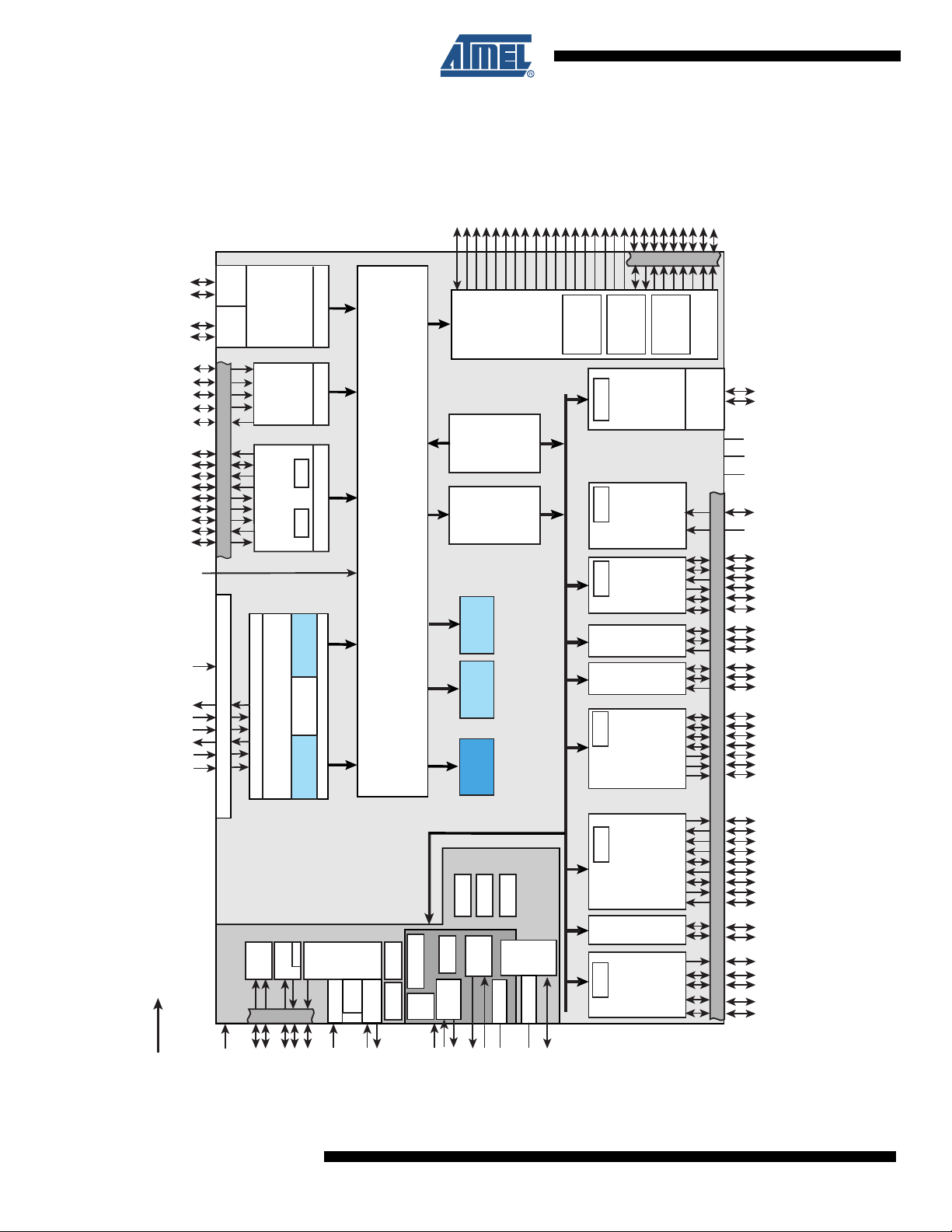
Figure 2-1. AT91SAM9260 Block Diagram
HDMB
HDPB
HDMA
HDPA
ISI_HSYNC
ISI_DO-ISI_D7
ISI_PCK
ISI_MCK
F100
MDIO
MDC
ETX0-ETX3
ERX0-ERX3
ERXER-ERXDV
ECRS-ECOL
ETXEN-ETXER
ETXCK-ERXCK
JTAGSEL
RTCK
TCK
TMS
TDO
TDI
NTRST
SLAVEMASTER
ISI_VSYNC
BMS
JTAG Selection and Boundary Scan
System
Transc.
Transc.
In-Circuit Emulator
AIC
Controller
USB
OHCI
Image
Sensor
MAC
10/100 Ethernet
ARM926EJ-S Processor
DBGU
DMA
DMA
Interface
FIFO
DMA
FIFO
6-layer Matrix
DCache
8 Kbytes
MMU
Bus Interface
ID
ICache
8 Kbytes
PDC
PMC
PLLA
PLLB
Filter
OSC
PITWDT
4GPREG
RC
A1/NBS2/NWR2
D0-D15
A0/NBS0
EBI
Fast SRAM
Fast SRAM
ROM
PIOA
RTT
OSC
A2-A15, A18-A20
A16/BA0
A17/BA1
NCS0
NCS1/SDCS
NAND Flash
CompactFlash
DMA
Peripheral
22-channel
Bridge
Peripheral
4 Kbytes
4 Kbytes
32 Kbytes
PIOC
PIOB
POR
RSTC
POR
SHDWC
NRD/CFOE
NWR0/NWE/CFWE
NWR1/NBS1/CFIOR
NWR3/NBS3/CFIOW
SDCK, SDCKE
RAS, CAS
SDWE, SDA10
SDRAM
Controller
APB
A21/NANDALE
A22/NANDCLE
NANDOE, NANDWE
Static
Memory
USB
DPRAM
PDC
4-channel
PDC
SSC
TC3
TC0
PDC
SPI0
PDC
USART0
PDC
MCI
A23-A24
NWAIT
D16-D31
Controller
Device
10-bit ADC
TC4
TC5
TC1
TC2
SPI1
USART1
USART2
USART3
TWI
NCS5/CFCS1
A25/CFRNW
NCS4/CFCS0
CFCE1-CFCE2
NCS2, NCS6, NCS7
ECC
Controller
Transceiver
USART4
USART5
NCS3/NANDCS
RK
RF
TD
TF
TK
VDDANA
ADVREF
RD
RI0
DDP
DDM
GNDANA
MISO
MOSI
SPCK
DTR0
DCD0
DSR0
TWD
ADTRIG
AD0-AD3
NPCS0
NPCS1
NPCS2
NPCS3
TWCK
MCCK
MCCDA
MCCDB
TIOB3-TIOB5
TIOA3-TIOA5
TCLK3-TCLK5
TIOB0-TIOB2
TIOA0-TIOA2
TCLK0-TCLK2
SPI0_, SPI1_
TXD0-TXD5
RXD0-RXD5
SCK0-SCK3
RTS0-RTS3
CTS0-CTS3
MCDA0-MCDA3
MCDB0-MCDB3
PLLRCA
XIN
XOUT
XIN32
XOUT32
OSCSEL
SHDN
WKUP
VDDBU
NRST
VDDCORE
FIQ
TST
4
AT91SAM9260
DTXD
DRXD
IRQ0-IRQ2
PCK0-PCK1
6221HS–ATARM–31-Jan-08

AT91SAM9260
3. Signal Description
Table 3-1. Signal Description List
Active
Signal Name Function Type
Power Supplies
VDDIOM EBI I/O Lines Power Supply Power 1.65V to 1.95V or 3.0V to3.6V
VDDIOP0 Peripherals I/O Lines Power Supply Power 3.0V to 3.6V
VDDIOP1 Peripherals I/O Lines Power Supply Power 1.65V to 3.6V
VDDBU Backup I/O Lines Power Supply Power 1.65V to 1.95V
VDDANA Analog Power Supply Power 3.0V to 3.6V
VDDPLL PLL Power Supply Power 1.65V to 1.95V
VDDCORE Core Chip Power Supply Power 1.65V to 1.95V
GND Ground Ground
GNDPLL PLL and Oscillator Ground Ground
GNDANA Analog Ground Ground
GNDBU Backup Ground Ground
Clocks, Oscillators and PLLs
XIN Main Oscillator Input Input
XOUT Main Oscillator Output Output
XIN32 Slow Clock Oscillator Input Input
XOUT32 Slow Clock Oscillator Output Output
OSCSEL Slow Clock Oscillator Selection Input
PLLRCA PLL A Filter Input
PCK0 - PCK1 Programmable Clock Output Output
Shutdown, Wakeup Logic
SHDN Shutdown Control Output
WKUP Wake-up Input Input
ICE and JTAG
NTRST Test Reset Signal Input Low Pull-up resistor
TCK Test Clock Input No pull-up resistor
TDI Test Data In Input No pull-up resistor
TDO Test Data Out Output
TMS Test Mode Select Input No pull-up resistor
JTAGSEL JTAG Selection Input
RTCK Return Test Clock Output
Level Comments
Accepts between 0V and
VDDBU.
Driven at 0V only. Do not tie
over VDDBU.
Accepts between 0V and
VDDBU.
Pull-down resistor. Accepts
between 0V and VDDBU.
6221HS–ATARM–31-Jan-08
5

Table 3-1. Signal Description List (Continued)
Active
Signal Name Function Type
Reset/Test
NRST Microcontroller Reset I/O Low Pull-up resistor
TST Test Mode Select Input
BMS Boot Mode Select Input
Debug Unit - DBGU
DRXD Debug Receive Data Input
DTXD Debug Transmit Data Output
Advanced Interrupt Controller - AIC
IRQ0 - IRQ2 External Interrupt Inputs Input
FIQ Fast Interrupt Input Input
PIO Controller - PIOA - PIOB - PIOC
PA0 - PA31 Parallel IO Controller A I/O Pulled-up input at reset
PB0 - PB31 Parallel IO Controller B I/O Pulled-up input at reset
PC0 - PC31 Parallel IO Controller C I/O Pulled-up input at reset
External Bus Interface - EBI
D0 - D31 Data Bus I/O Pulled-up input at reset
A0 - A25 Address Bus Output 0 at reset
NWAIT External Wait Signal Input Low
Static Memory Controller - SMC
NCS0 - NCS7 Chip Select Lines Output Low
NWR0 - NWR3 Write Signal Output Low
NRD Read Signal Output Low
NWE Write Enable Output Low
NBS0 - NBS3 Byte Mask Signal Output Low
CompactFlash Support
CFCE1 - CFCE2 CompactFlash Chip Enable Output Low
CFOE CompactFlash Output Enable Output Low
CFWE CompactFlash Write Enable Output Low
CFIOR CompactFlash IO Read Output Low
CFIOW CompactFlash IO Write Output Low
CFRNW CompactFlash Read Not Write Output
CFCS0 - CFCS1 CompactFlash Chip Select Lines Output Low
Level Comments
Pull-down resistor. Accepts
between 0V and VDDBU.
6
AT91SAM9260
6221HS–ATARM–31-Jan-08

Table 3-1. Signal Description List (Continued)
Active
Signal Name Function Type
NAND Flash Support
NANDCS NAND Flash Chip Select Output Low
NANDOE NAND Flash Output Enable Output Low
NANDWE NAND Flash Write Enable Output Low
NANDALE NAND Flash Address Latch Enable Output Low
NANDCLE NAND Flash Command Latch Enable Output Low
SDRAM Controller
SDCK SDRAM Clock Output
SDCKE SDRAM Clock Enable Output High
SDCS SDRAM Controller Chip Select Output Low
BA0 - BA1 Bank Select Output
SDWE SDRAM Write Enable Output Low
RAS - CAS Row and Column Signal Output Low
SDA10 SDRAM Address 10 Line Output
Multimedia Card Interface MCI
MCCK Multimedia Card Clock Output
MCCDA Multimedia Card Slot A Command I/O
MCDA0 - MCDA3 Multimedia Card Slot A Data I/O
MCCDB Multimedia Card Slot B Command I/O
MCDB0 - MCDB3 Multimedia Card Slot B Data I/O
Universal Synchronous Asynchronous Receiver Transmitter USARTx
SCKx USARTx Serial Clock I/O
TXDx USARTx Transmit Data I/O
RXDx USARTx Receive Data Input
RTSx USARTx Request To Send Output
CTSx USARTx Clear To Send Input
DTR0 USART0 Data Terminal Ready Output
DSR0 USART0 Data Set Ready Input
DCD0 USART0 Data Carrier Detect Input
RI0 USART0 Ring Indicator Input
Synchronous Serial Controller - SSC
TD SSC Transmit Data Output
RD SSC Receive Data Input
TK SSC Transmit Clock I/O
RK SSC Receive Clock I/O
TF SSC Transmit Frame Sync I/O
RF SSC Receive Frame Sync I/O
Level Comments
AT91SAM9260
6221HS–ATARM–31-Jan-08
7

Table 3-1. Signal Description List (Continued)
Active
Signal Name Function Type
Timer/Counter - TCx
TCLKx TC Channel x External Clock Input Input
TIOAx TC Channel x I/O Line A I/O
TIOBx TC Channel x I/O Line B I/O
Serial Peripheral Interface - SPIx_
SPIx_MISO Master In Slave Out I/O
SPIx_MOSI Master Out Slave In I/O
SPIx_SPCK SPI Serial Clock I/O
SPIx_NPCS0 SPI Peripheral Chip Select 0 I/O Low
SPIx_NPCS1-SPIx_NPCS3 SPI Peripheral Chip Select Output Low
Two-Wire Interface
TWD Two-wire Serial Data I/O
TWCK Two-wire Serial Clock I/O
USB Host Port
HDPA USB Host Port A Data + Analog
HDMA USB Host Port A Data - Analog
HDPB USB Host Port B Data + Analog
HDMB USB Host Port B Data + Analog
USB Device Port
DDM USB Device Port Data - Analog
DDP USB Device Port Data + Analog
Ethernet 10/100
ETXCK Transmit Clock or Reference Clock Input MII only, REFCK in RMII
ERXCK Receive Clock Input MII only
ETXEN Transmit Enable Output
ETX0-ETX3 Transmit Data Output ETX0-ETX1 only in RMII
ETXER Transmit Coding Error Output MII only
ERXDV Receive Data Valid Input RXDV in MII , CRSDV in RMII
ERX0-ERX3 Receive Data Input ERX0-ERX1 only in RMII
ERXER Receive Error Input
ECRS Carrier Sense and Data Valid Input MII only
ECOL Collision Detect Input MII only
EMDC Management Data Clock Output
EMDIO Management Data Input/Output I/O
EF100 Force 100Mbit/sec. Output High
Level Comments
8
AT91SAM9260
6221HS–ATARM–31-Jan-08
Table 3-1. Signal Description List (Continued)
Signal Name Function Type
Image Sensor Interface
ISI_D0-ISI_D11 Image Sensor Data Input
ISI_MCK Image Sensor Reference Clock Output
ISI_HSYNC Image Sensor Horizontal Synchro Input
ISI_VSYNC Image Sensor Vertical Synchro Input
ISI_PCK Image Sensor Data clock Input
Analog to Digital Converter
AD0-AD3 Analog Inputs Analog
ADVREF Analog Positive Reference Analog
ADTRG ADC Trigger Input
AT91SAM9260
Active
Level Comments
Digital pulled-up inputs at
reset
6221HS–ATARM–31-Jan-08
9

4. Package and Pinout
The AT91SAM9260 is available in two packages:
• 208-pin PQFP Green package (0.5mm pitch) (Figure 4-1)
• 217-ball LFBGA Green package (0.8 mm ball pitch) (Figure 4-2).
4.1 208-pin PQFP Package Outline
Figure 4-1 shows the orientation of the 208-pin PQFP package.
A detailed mechanical description is given in the section “AT91SAM9260 Mechanical Characteristics” of the product datasheet.
Figure 4-1. 208-pin PQFP Package
105156
157
208
104
53
152
10
AT91SAM9260
6221HS–ATARM–31-Jan-08

AT91SAM9260
4.2 208-pin PQFP Pinout
Table 4-1. Pinout for 208-pin PQFP Package
Pin Signal Name Pin Signal Name Pin Signal Name Pin Signal Name
1 PA24 53 GND 105 RAS 157 ADVREF
2 PA25 54 DDM 106 D0 158 PC0
3 PA26 55 DDP 107 D1 159 PC1
4 PA27 56 PC13 108 D2 160 VDDANA
5 VDDIOP0 57 PC11 109 D3 161 PB10
6 GND 58 PC10 110 D4 162 PB11
7 PA28 59 PC14 111 D5 163 PB20
8 PA29 60 PC9 112 D6 164 PB21
9 PB0 61 PC8 113 GND 165 PB22
10 PB1 62 PC4 114 VDDIOM 166 PB23
11 PB2 63 PC6 115 SDCK 167 PB24
12 PB3 64 PC7 116 SDWE 168 PB25
13 VDDIOP0 65 VDDIOM 117 SDCKE 169 VDDIOP1
14 GND 66 GND 118 D7 170 GND
15 PB4 67 PC5 119 D8 171 PB26
16 PB5 68 NCS0 120 D9 172 PB27
17 PB6 69 CFOE/NRD 121 D10 173 GND
18 PB7 70 CFWE/NWE/NWR0 122 D11 174 VDDCORE
19 PB8 71 NANDOE 123 D12 175 PB28
20 PB9 72 NANDWE 124 D13 176 PB29
21 PB14 73 A22 125 D14 177 PB30
22 PB15 74 A21 126 D15 178 PB31
23 PB16 75 A20 127 PC15 179 PA0
24 VDDIOP0 76 A19 128 PC16 180 PA1
25 GND 77 VDDCORE 129 PC17 181 PA2
26 PB17 78 GND 130 PC18 182 PA3
27 PB18 79 A18 131 PC19 183 PA4
28 PB19 80 BA1/A17 132 VDDIOM 184 PA5
29 TDO 81 BA0/A16 133 GND 185 PA6
30 TDI 82 A15 134 PC20 186 PA7
31 TMS 83 A14 135 PC21 187 VDDIOP0
32 VDDIOP0 84 A13 136 PC22 188 GND
33 GND 85 A12 137 PC23 189 PA8
34 TCK 86 A11 138 PC24 190 PA9
35 NTRST 87 A10 139 PC25 191 PA10
36 NRST 88 A9 140 PC26 192 PA11
37 RTCK 89 A8 141 PC27 193 PA12
38 VDDCORE 90 VDDIOM 142 PC28 194 PA13
39 GND 91 GND 143 PC29 195 PA14
40 BMS 92 A7 144 PC30 196 PA15
41 OSCSEL 93 A6 145 PC31 197 PA16
42 TST 94 A5 146 GND 198 PA17
43 JTAGSEL 95 A4 147 VDDCORE 199 VDDIOP0
44 GNDBU 96 A3 148 VDDPLL 200 GND
45 XOUT32 97 A2 149 XIN 201 PA18
46 XIN32 98 NWR2/NBS2/A1 150 XOUT 202 PA19
47 VDDBU 99 NBS0/A0 151 GNDPLL 203 VDDCORE
48 WKUP 100 SDA10 152 NC 204 GND
6221HS–ATARM–31-Jan-08
11
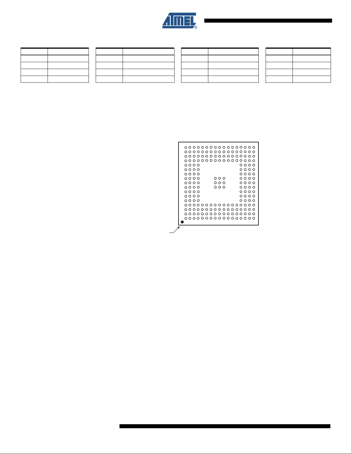
Table 4-1. Pinout for 208-pin PQFP Package (Continued)
Pin Signal Name Pin Signal Name Pin Signal Name Pin Signal Name
49 SHDN 101 CFIOW/NBS3/NWR3 153 GNDPLL 205 PA20
50 HDMA 102 CFIOR/NBS1/NWR1 154 PLLRCA 206 PA21
51 HDPA 103 SDCS/NCS1 155 VDDPLL 207 PA22
52 VDDIOP0 104 CAS 156 GNDANA 208 PA23
4.3 217-ball LFBGA Package Outline
Figure 4-2 shows the orientation of the 217-ball LFBGA package.
A detailed mechanical description is given in the section “AT91SAM9260 Mechanical Characteristics” of the product datasheet.
Figure 4-2.
217-ball LFBGA Package (Top View)
17
16
15
14
13
12
11
10
9
8
7
6
5
4
3
2
1
Ball A1
ABCDEFGHJ K LMNPRTU
12
AT91SAM9260
6221HS–ATARM–31-Jan-08
AT91SAM9260
4.4 217-ball LFBGA Pinout
Table 4-2. Pinout for 217-ball LFBGA Package
Pin Signal Name Pin Signal Name Pin Signal Name Pin Signal Name
A1 CFIOW/NBS3/NWR3 D5 A5 J14 TDO P17 PB5
A2 NBS0/A0 D6 GND J15 PB19 R1 NC
A3 NWR2/NBS2/A1 D7 A10 J16 TDI R2 GNDANA
A4 A6 D8 GND J17 PB16 R3 PC29
A5 A8 D9 VDDCORE K1 PC24 R4 VDDANA
A6 A11 D10 GND K2 PC20 R5 PB12
A7 A13 D11 VDDIOM K3 D15 R6 PB23
A8 BA0/A16 D12 GND K4 PC21 R7 GND
A9 A18 D13 DDM K8 GND R8 PB26
A10 A21 D14 HDPB K9 GND R9 PB28
A11 A22 D15 NC K10 GND R10 PA0
A12 CFWE/NWE/NWR0 D16 VDDBU K14 PB4 R11 PA4
A13 CFOE/NRD D17 XIN32 K15 PB17 R12 PA5
A14 NCS0 E1 D10 K16 GND R13 PA10
A15 PC5 E2 D5 K17 PB15 R14 PA21
A16 PC6 E3 D3 L1 GND R15 PA23
A17 PC4 E4 D4 L2 PC26 R16 PA24
B1 SDCK E14 HDPA L3 PC25 R17 PA29
B2 CFIOR/NBS1/NWR1 E15 HDMA L4 VDDIOP0 T1 PLLRCA
B3 SDCS/NCS1 E16 GNDBU L14 PA28 T2 GNDPLL
B4 SDA10 E17 XOUT32 L15 PB9 T3 PC0
B5 A3 F1 D13 L16 PB8 T4 PC1
B6 A7 F2 SDWE L17 PB14 T5 PB10
B7 A12 F3 D6 M1 VDDCORE T6 PB22
B8 A15 F4 GND M2 PC31 T7 GND
B9 A20 F14 OSCSEL M3 GND T8 PB29
B10 NANDWE F15 BMS M4 PC22 T9 PA2
B11 PC7 F16 JTAGSEL M14 PB1 T10 PA6
B12 PC10 F17 TST M15 PB2 T11 PA8
B13 PC13 G1 PC15 M16 PB3 T12 PA11
B14 PC11 G2 D7 M17 PB7 T13 VDDCORE
B15 PC14 G3 SDCKE N1 XIN T14 PA20
B16 PC8 G4 VDDIOM N2 VDDPLL T15 GND
B17 WKUP G14 GND N3 PC23 T16 PA22
C1 D8 G15 NRST N4 PC27 T17 PA27
C2 D1 G16 RTCK N14 PA31 U1 GNDPLL
C3 CAS G17 TMS N15 PA30 U2 ADVREF
C4 A2 H1 PC18 N16 PB0 U3 PC2
C5 A4 H2 D14 N17 PB6 U4 PC3
C6 A9 H3 D12 P1 XOUT U5 PB20
C7 A14 H4 D11 P2 VDDPLL U6 PB21
C8 BA1/A17 H8 GND P3 PC30 U7 PB25
C9 A19 H9 GND P4 PC28 U8 PB27
C10 NANDOE H10 GND P5 PB11 U9 PA12
C11 PC9 H14 VDDCORE P6 PB13 U10 PA13
C12 PC12 H15 TCK P7 PB24 U11 PA14
C13 DDP H16 NTRST P8 VDDIOP1 U12 PA15
C14 HDMB H17 PB18 P9 PB30 U13 PA19
C15 NC J1 PC19 P10 PB31 U14 PA17
6221HS–ATARM–31-Jan-08
13

Table 4-2. Pinout for 217-ball LFBGA Package (Continued)
Pin Signal Name Pin Signal Name Pin Signal Name Pin Signal Name
C16 VDDIOP0 J2 PC17 P11 PA1 U15 PA16
C17 SHDN J3 VDDIOM P12 PA3 U16 PA18
D1 D9 J4 PC16 P13 PA7 U17 VDDIOP0
D2 D2 J8 GND P14 PA9
D3 RAS J9 GND P15 PA26
D4 D0 J10 GND P16 PA25
5. Power Considerations
5.1 Power Supplies
The AT91SAM9260 has several types of power supply pins:
• VDDCORE pins: Power the core, including the processor, the embedded memories and the
peripherals; voltage ranges from 1.65V and 1.95V, 1.8V nominal.
• VDDIOM pins: Power the External Bus Interface I/O lines; voltage ranges between 1.65V and
1.95V (1.8V typical) or between 3.0V and 3.6V (3.3V nominal). The expected voltage range is
selectable by software.
• VDDIOP0 pins: Power the Peripheral I/O lines and the USB transceivers; voltage ranges from
3.0V and 3.6V, 3V or 3.3V nominal.
• VDDIOP1 pins: Power the Peripherals I/O lines involving the Image Sensor Interface; voltage
ranges from 1.65V and 3.6V, 1.8V, 2.5V, 3V or 3.3V nominal.
• VDDBU pin: Powers the Slow Clock oscillator and a part of the System Controller; voltage
ranges from 1.65V to 1.95V, 1.8V nominal.
• VDDPLL pin: Powers the Main Oscillator and PLL cells; voltage ranges from 1.65V and
1.95V, 1.8V nominal.
• VDDANA pin: Powers the Analog to Digital Converter; voltage ranges from 3.0V and 3.6V,
3.3V nominal.
The power supplies VDDIOM, VDDIOP0 and VDDIOP1 are identified in the pinout table and the
multiplexing tables. These supplies enable the user to power the device differently for interfacing
with memories and for interfacing with peripherals.
Ground pins GND are common to VDDCORE, VDDIOM, VDDIOP0 and VDDIOP1 pins power
supplies. Separated ground pins are provided for VDDBU, VDDPLL and VDDANA. These
ground pins are respectively GNDBU, GNDPLL and GNDANA.
5.2 Power Consumption
The AT91SAM9260 consumes about 500 µA of static current on VDDCORE at 25°C. This static
current rises up to 5 mA if the temperature increases to 85°C.
On VDDBU, the current does not exceed 10 µA in worst case conditions.
For dynamic power consumption, the AT91SAM9260 consumes a maximum of 100 mA on
VDDCORE at maximum conditions (1.8V, 25°C, processor running full-performance algorithm
out of high speed memories).
14
AT91SAM9260
6221HS–ATARM–31-Jan-08

5.3 Programmable I/O Lines Power Supplies
The power supplies pins VDDIOM accept two voltage ranges. This allows the device to reach its
maximum speed either out of 1.8V or 3.3V external memories.
The target maximum speed is 100 MHz on the pin SDCK (SDRAM Clock) loaded with 30 pF for
power supply at 1.8V and 50 pF for power supply at 3.3V. The other signals (control, address
and data signals) do not exceed 50 MHz.
The voltage ranges are determined by programming registers in the Chip Configuration registers
located in the Matrix User Interface.
At reset, the selected voltage defaults to 3.3V nominal, and power supply pins can accept either
1.8V or 3.3V. Obviously, the device cannot reach its maximum speed if the voltage supplied to
the pins is 1.8V only. The user must program the EBI voltage range before getting the device out
of its Slow Clock Mode.
6. I/O Line Considerations
6.1 JTAG Port Pins
TMS, TDI and TCK are Schmitt trigger inputs and have no pull-up resistors.
AT91SAM9260
6.2 Test Pin
6.3 Reset Pins
TDO and RTCK are outputs, driven at up to VDDIOP0, and have no pull-up resistors.
The JTAGSEL pin is used to select the JTAG boundary scan when asserted at a high level (tied
to VDDBU). It integrates a permanent pull-down resistor of about 15 kΩ to GNDBU, so that it
can be left unconnected for normal operations.
The NTRST signal is described in Section 6.3.
All the JTAG signals are supplied with VDDIOP0.
The TST pin is used for manufacturing test purposes when asserted high. It integrates a permanent pull-down resistor of about 15 kΩ to GNDBU, so that it can be left unconnected for normal
operations. Driving this line at a high level leads to unpredictable results.
This pin is supplied with VDDBU.
NRST is a bidirectional with an open-drain output integrating a non-programmable pull-up resistor. It can be driven with voltage at up to VDDIOP0.
NTRST is an input which allows reset of the JTAG Test Access port. It has no action on the
processor.
As the product integrates power-on reset cells, which manages the processor and the JTAG
reset, the NRST and NTRST pins can be left unconnected.
6221HS–ATARM–31-Jan-08
The NRST and NTRST pins both integrate a permanent pull-up resistor to VDDIOP0. Its value
can be found in the table “DC Characteristics” in the section “AT91SAM9260 Electrical Characteristics” in the product datasheet.
The NRST signal is inserted in the Boundary Scan.
15

6.4 PIO Controllers
All the I/O lines managed by the PIO Controllers integrate a programmable pull-up resistor.
Refer to the section on DC Characteristics in “AT91SAM9260 Electrical Characteristics” for
more information. Programming of this pull-up resistor is performed independently for each I/O
line through the PIO Controllers.
After reset, all the I/O lines default as inputs with pull-up resistors enabled, except those which
are multiplexed with the External Bus Interface signals and that must be enabled as Peripheral
at reset. This is explicitly indicated in the column “Reset State” of the PIO Controller multiplexing
tables.
6.5 I/O Line Drive Levels
The PIO lines are high-drive current capable. Each of these I/O lines can drive up to 16 mA permanently except PC4 to PC31 that are VDDIOM powered.
6.6 Shutdown Logic Pins
The SHDN pin is an output only, which is driven by the Shutdown Controller.
The pin WKUP is an input-only. It can accept voltages only between 0V and VDDBU.
6.7 Slow Clock Selection
The AT91SAM9260 slow clock can be generated either by an external 32,768 Hz crystal or the
on-chip RC oscillator.
Table 6-1 defines the states for OSCSEL signal.
Table 6-1. Slow Clock Selection
OSCSEL Slow Clock Startup Time
0 Internal RC 240 µs
1 External 32768 Hz 1200 ms
The startup counter delay for the slow clock oscillator depends on the OSCSEL signal. The
32,768 Hz startup delay is 1200 ms whereas it is 240 µs for the internal RC oscillator (refer to
Table 6-1). The pin OSCSEL must be tied either to GND or VDDBU for correct operation of the
device.
7. Processor and Architecture
7.1 ARM926EJ-S Processor
• RISC Processor Based on ARM v5TEJ Architecture with Jazelle technology for Java
acceleration
• Two Instruction Sets
– ARM High-performance 32-bit Instruction Set
– Thumb High Code Density 16-bit Instruction Set
• DSP Instruction Extensions
• 5-Stage Pipeline Architecture:
– Instruction Fetch (F)
16
AT91SAM9260
6221HS–ATARM–31-Jan-08

AT91SAM9260
– Instruction Decode (D)
– Execute (E)
– Data Memory (M)
– Register Write (W)
• 8-Kbyte Data Cache, 8-Kbyte Instruction Cache
– Virtually-addressed 4-way Associative Cache
– Eight words per line
– Write-through and Write-back Operation
– Pseudo-random or Round-robin Replacement
• Write Buffer
– Main Write Buffer with 16-word Data Buffer and 4-address Buffer
– DCache Write-back Buffer with 8-word Entries and a Single Address Entry
– Software Control Drain
• Standard ARM v4 and v5 Memory Management Unit (MMU)
– Access Permission for Sections
– Access Permission for large pages and small pages can be specified separately for
each quarter of the page
– 16 embedded domains
• Bus Interface Unit (BIU)
– Arbitrates and Schedules AHB Requests
– Separate Masters for both instruction and data access providing complete Matrix
system flexibility
– Separate Address and Data Buses for both the 32-bit instruction interface and the
32-bit data interface
– On Address and Data Buses, data can be 8-bit (Bytes), 16-bit (Half-words) or 32-bit
(Words)
7.2 Bus Matrix
6221HS–ATARM–31-Jan-08
• 6-layer Matrix, handling requests from 6 masters
• Programmable Arbitration strategy
– Fixed-priority Arbitration
– Round-Robin Arbitration, either with no default master, last accessed default master
or fixed default master
• Burst Management
– Breaking with Slot Cycle Limit Support
– Undefined Burst Length Support
• One Address Decoder provided per Master
– Three different slaves may be assigned to each decoded memory area: one for
internal boot, one for external boot, one after remap
• Boot Mode Select
– Non-volatile Boot Memory can be internal or external
– Selection is made by BMS pin sampled at reset
17

7.2.1 Matrix Masters
7.2.2 Matrix Slaves
• Remap Command
– Allows Remapping of an Internal SRAM in Place of the Boot Non-Volatile Memory
– Allows Handling of Dynamic Exception Vectors
The Bus Matrix of the AT91SAM9260 manages six Masters, which means that each master can
perform an access concurrently with others, according the slave it accesses is available.
Each Master has its own decoder that can be defined specifically for each master. In order to
simplify the addressing, all the masters have the same decodings.
Table 7-1. List of Bus Matrix Masters
Master 0 ARM926™ Instruction
Master 1 ARM926 Data
Master 2 PDC
Master 3 USB Host DMA
Master 4 ISI Controller
Master 5 Ethernet MAC
Each Slave has its own arbiter, thus allowing a different arbitration per Slave to be programmed.
Table 7-2. List of Bus Matrix Slaves
Slave 0 Internal SRAM0 4 KBytes
Slave 1 Internal SRAM1 4 KBytes
Slave 2
Slave 3 External Bus Interface
Slave 4 Internal Peripherals
7.2.3 Master to Slave Access
All the Masters can normally access all the Slaves. However, some paths do not make sense,
such as allowing access from the Ethernet MAC to the Internal Peripherals. Thus, these paths
are forbidden or simply not wired, and shown “-” in the following table.
Table 7-3. AT91SAM9260 Masters to Slaves Access
0
1
Internal ROM
USB Host User Interface
Master 0 & 12345
Slave
Internal SRAM
4 KBytes
Internal SRAM
4 KBytes
ARM926
Instruction &
Data
X XXXX
X XXXX
Peripheral
DMA
Controller
USB Host
Controller
ISI
Controller
Ethernet
MAC
18
AT91SAM9260
6221HS–ATARM–31-Jan-08

Table 7-3. AT91SAM9260 Masters to Slaves Access
AT91SAM9260
2
3External Bus InterfaceX XXXX
4 Internal Peripherals X X X - -
Internal ROM X X X - -
UHP User InterfaceX ----
7.3 Peripheral DMA Controller
• Acting as one Matrix Master
• Allows data transfers from/to peripheral to/from any memory space without any intervention
of the processor.
• Next Pointer Support, forbids strong real-time constraints on buffer management.
• Twenty-two channels
– Two for each USART
– Two for the Debug Unit
– Two for each Serial Synchronous Controller
– Two for each Serial Peripheral Interface
– One for Multimedia Card Interface
– One for Analog-to-Digital Converter
The Peripheral DMA Controller handles transfer requests from the channel according to the following priorities (Low to High priorities):
– DBGU Transmit Channel
– USART5 Transmit Channel
– USART4 Transmit Channel
– USART3 Transmit Channel
– USART2 Transmit Channel
– USART1 Transmit Channel
– USART0 Transmit Channel
– SPI1 Transmit Channel
– SPI0 Transmit Channel
– SSC Transmit Channel
– DBGU Receive Channel
– USART5 Receive Channel
– USART4 Receive Channel
– USART3 Receive Channel
– USART2 Receive Channel
– USART1 Receive Channel
– USART0 Receive Channel
– ADC Receive Channel
– SPI1 Receive Channel
– SPI0 Receive Channel
– SSC Receive Channel
6221HS–ATARM–31-Jan-08
19

– MCI Transmit/Receive Channel
7.4 Debug and Test Features
• ARM926 Real-time In-circuit Emulator
– Two real-time Watchpoint Units
– Two Independent Registers: Debug Control Register and Debug Status Register
– Test Access Port Accessible through JTAG Protocol
– Debug Communications Channel
• Debug Unit
–Two-pin UART
– Debug Communication Channel Interrupt Handling
– Chip ID Register
• IEEE1149.1 JTAG Boundary-scan on All Digital Pins
20
AT91SAM9260
6221HS–ATARM–31-Jan-08

8. Memories
Figure 8-1. AT91SAM9260 Memory Mapping
Address Memory Space
0x0000 0000
0x0FFF FFFF
0x1000 0000
0x1FFF FFFF
0x2000 0000
0x2FFF FFFF
0x3000 0000
0x3FFF FFFF
0x4000 0000
0x4FFF FFFF
0x5000 0000
0x5FFF FFFF
0x6000 0000
0x6FFF FFFF
0x7000 0000
0x7FFF FFFF
0x8000 0000
0x8FFF FFFF
0x9000 0000
0xEFFF FFFF
0xF000 0000
0xFFFF FFFF
Internal Memories
EBI
Chip Select 0
EBI
Chip Select 1/
SDRAMC
EBI
Chip Select 2
EBI
Chip Select 3/
NANDFlash
EBI
Chip Select 4/
Compact Flash
Slot 0
EBI
Chip Select 5/
Compact Flash
Slot 1
EBI
Chip Select 6
EBI
Chip Select 7
Undefined
(Abort)
Internal Peripherals
256M Bytes
256M Bytes
256M Bytes
256M Bytes
256M Bytes
256M Bytes
256M Bytes
256M Bytes
256M Bytes
1,518M Bytes
256M Bytes
0xF000 0000
0xFFFA 0000
0xFFFA 4000
0xFFFA 8000
0xFFFA C000
0xFFFB 0000
0xFFFB 4000
0xFFFB 8000
0xFFFB C000
0xFFFC 0000
0xFFFC 4000
0xFFFC 8000
0xFFFC C000
0xFFFD 0000
0xFFFD 4000
0xFFFD 8000
0xFFFD C000
0xFFFE 0000
0xFFFE 4000
0xFFFF C000
0xFFFF FFFF
0x0000 0000
0x10 0000
0x10 8000
0x20 0000
0x20 1000
0x30 0000
0x30 1000
0x50 0000
0x50 4000
0x0FFF FFFF
Internal Memory Mapping
Boot Memory (1)
ROM
Reserved
SRAM0
Reserved
SRAM1
Reserved
UHP
Reserved
Peripheral Mapping
Reserved
TCO, TC1, TC2
UDP
MCI
TWI
USART0
USART1
USART2
SSC
ISI
EMAC
SPI0
SPI1
USART3
USART4
USART5
TC3, TC4, TC5
ADC
Reserved
SYSC
16K Bytes
16K Bytes
16K Bytes
16K Bytes
16K Bytes
16K Bytes
16K Bytes
16K Bytes
16K Bytes
16K Bytes
16K Bytes
16K Bytes
16K Bytes
16K Bytes
16K Bytes
16K Bytes
16K Bytes
16K Bytes
32K Bytes
4K Bytes
4K Bytes
16K Bytes
AT91SAM9260
Notes :
(1) Can be ROM, EBI_NCS0 or SRAM
depending on BMS and REMAP
System Controller Mapping
0xFFFF C000
0xFFFF E800
0xFFFF EA00
0xFFFF EC00
0xFFFF EE00
0xFFFF EF10
0xFFFF F000
0xFFFF F200
0xFFFF F400
0xFFFF F600
0xFFFF F800
0xFFFF FA00
0xFFFF FC00
0xFFFF FD00
0xFFFF FD10
0xFFFF FD20
0xFFFF FD30
0xFFFF FD40
0xFFFF FD50
0xFFFF FD60
0xFFFF FFFF
Reserved
ECC 512 Bytes
512 BytesSDRAMC
512 BytesSMC
MATRIX
CCFG
AIC
DBGU
PIOA
PIOB
PIOC
Reserved
PMC
RSTC
SHDWC
RTTC
PITC
WDTC
GPBR
Reserved
512 Bytes
512 Bytes
512 Bytes
512 Bytes
512 bytes
512 bytes
256 Bytes
16 Bytes
16 Bytes
16 Bytes
16 Bytes
16 Bytes
16 Bytes
6221HS–ATARM–31-Jan-08
21
A first level of address decoding is performed by the Bus Matrix, i.e., the implementation of the
Advanced High Performance Bus (AHB) for its Master and Slave interfaces with additional
features.
Decoding breaks up the 4G bytes of address space into 16 banks of 256 Mbytes. The banks 1 to
7 are directed to the EBI that associates these banks to the external chip selects EBI_NCS0 to
EBI_NCS7. Bank 0 is reserved for the addressing of the internal memories, and a second level
of decoding provides 1 Mbyte of internal memory area. Bank 15 is reserved for the peripherals
and provides access to the Advanced Peripheral Bus (APB).
Other areas are unused and performing an access within them provides an abort to the master
requesting such an access.
Each Master has its own bus and its own decoder, thus allowing a different memory mapping
per Master. However, in order to simplify the mappings, all the masters have a similar address
decoding.
Regarding Master 0 and Master 1 (ARM926 Instruction and Data), three different Slaves are
assigned to the memory space decoded at address 0x0: one for internal boot, one for external
boot, one after remap. Refer to Table 8-1, “Internal Memory Mapping,” on page 22 for details.
A complete memory map is presented in Figure 8-1 on page 21.
8.1 Embedded Memories
• 32 KB ROM
– Single Cycle Access at full matrix speed
• Two 4 KB Fast SRAM
– Single Cycle Access at full matrix speed
8.1.1 Boot Strategies
Table 8-1 summarizes the Internal Memory Mapping for each Master, depending on the Remap
status and the BMS state at reset.
Table 8-1. Internal Memory Mapping
Address
0x0000 0000 ROM EBI_NCS0 SRAM0 4K
The system always boots at address 0x0. To ensure a maximum number of possibilities for boot,
the memory layout can be configured with two parameters.
REMAP allows the user to lay out the first internal SRAM bank to 0x0 to ease development. This
is done by software once the system has booted. Refer to the Bus Matrix Section for more
details.
When REMAP = 0, BMS allows the user to lay out to 0x0, at his convenience, the ROM or an
external memory. This is done via hardware at reset.
Note: Memory blocks not affected by these parameters can always be seen at their specified base
addresses. See the complete memory map presented in
REMAP = 0 REMAP = 1
BMS = 1 BMS = 0
Figure 8-1 on page 21.
22
AT91SAM9260
6221HS–ATARM–31-Jan-08

The AT91SAM9260 matrix manages a boot memory that depends on the level on the BMS pin
at reset. The internal memory area mapped between address 0x0 and 0x000F FFFF is reserved
for this purpose.
If BMS is detected at 1, the boot memory is the embedded ROM.
If BMS is detected at 0, the boot memory is the memory connected on the Chip Select 0 of the
External Bus Interface.
8.1.1.1 BMS = 1, Boot on Embedded ROM
The system boots using the Boot Program.
• Boot on slow clock (On-chip RC or 32,768 Hz)
• Auto baudrate detection
• Downloads and runs an application from external storage media into internal SRAM
• Downloaded code size depends on embedded SRAM size
• Automatic detection of valid application
• Bootloader on a non-volatile memory
– SPI DataFlash
– 8-bit and/or 16-bit NANDFlash
• SAM-BA
®
Boot in case no valid program is detected in external NVM, supporting
– Serial communication on a DBGU
– USB Device Port
®
connected on NPCS0 and NPCS1 of the SPI0
AT91SAM9260
8.1.1.2 BMS = 0, Boot on External Memory
• Boot on slow clock (On-chip RC or 32,768 Hz)
• Boot with the default configuration for the Static Memory Controller, byte select mode, 16-bit
data bus, Read/Write controlled by Chip Select, allows boot on 16-bit non-volatile memory.
The customer-programmed software must perform a complete configuration.
To speed up the boot sequence when booting at 32 kHz EBI CS0 (BMS=0), the user must take
the following steps:
1. Program the PMC (main oscillator enable or bypass mode).
2. Program and start the PLL.
3. Reprogram the SMC setup, cycle, hold, mode timings registers for CS0 to adapt them
to the new clock.
4. Switch the main clock to the new value.
8.2 External Memories
The external memories are accessed through the External Bus Interface. Each Chip Select line
has a 256-Mbyte memory area assigned.
Refer to the memory map in Figure 8-1 on page 21.
8.2.1 External Bus Interface
• Integrates three External Memory Controllers
– Static Memory Controller
– SDRAM Controller
6221HS–ATARM–31-Jan-08
23

– ECC Controller
• Additional logic for NANDFlash
• Full 32-bit External Data Bus
• Up to 26-bit Address Bus (up to 64MBytes linear)
• Up to 8 chip selects, Configurable Assignment:
– Static Memory Controller on NCS0
– SDRAM Controller or Static Memory Controller on NCS1
– Static Memory Controller on NCS2
– Static Memory Controller on NCS3, Optional NAND Flash support
– Static Memory Controller on NCS4 - NCS5, Optional CompactFlash support
– Static Memory Controller on NCS6-NCS7
8.2.2 Static Memory Controller
• 8-, 16- or 32-bit Data Bus
• Multiple Access Modes supported
– Byte Write or Byte Select Lines
– Asynchronous read in Page Mode supported (4- up to 32-byte page size)
• Multiple device adaptability
– Compliant with LCD Module
– Control signals programmable setup, pulse and hold time for each Memory Bank
• Multiple Wait State Management
– Programmable Wait State Generation
– External Wait Request
– Programmable Data Float Time
• Slow Clock mode supported
8.2.3 SDRAM Controller
• Supported devices
• Numerous configurations supported
• Programming facilities
• Energy-saving capabilities
24
AT91SAM9260
– Standard and Low-power SDRAM (Mobile SDRAM)
– 2K, 4K, 8K Row Address Memory Parts
– SDRAM with two or four Internal Banks
– SDRAM with 16- or 32-bit Datapath
– Word, half-word, byte access
– Automatic page break when Memory Boundary has been reached
– Multibank Ping-pong Access
– Timing parameters specified by software
– Automatic refresh operation, refresh rate is programmable
– Self-refresh, power down and deep power down modes supported
6221HS–ATARM–31-Jan-08

• Error detection
– Refresh Error Interrupt
• SDRAM Power-up Initialization by software
• CAS Latency of 1, 2 and 3 supported
• Auto Precharge Command not used
8.2.4 Error Corrected Code Controller
• Tracking the accesses to a NAND Flash device by trigging on the corresponding chip select
• Single bit error correction and 2-bit Random detection
• Automatic Hamming Code Calculation while writing
– ECC value available in a register
• Automatic Hamming Code Calculation while reading
– Error Report, including error flag, correctable error flag and word address being
detected erroneous
– Support 8- or 16-bit NAND Flash devices with 512-, 1024-, 2048- or 4096-bytes
pages
AT91SAM9260
6221HS–ATARM–31-Jan-08
25

9. System Controller
The System Controller is a set of peripherals that allows handling of key elements of the system,
such as power, resets, clocks, time, interrupts, watchdog, etc.
The System Controller User Interface also embeds the registers that configure the Matrix and a
set of registers for the chip configuration. The chip configuration registers configure EBI chip
select assignment and voltage range for external memories
The System Controller’s peripherals are all mapped within the highest 16 Kbytes of address
space, between addresses 0xFFFF E800 and 0xFFFF FFFF.
However, all the registers of System Controller are mapped on the top of the address space. All
the registers of the System Controller can be addressed from a single pointer by using the standard ARM instruction set, as the Load/Store instruction has an indexing mode of ±4 Kbytes.
Figure 9-1 on page 27 shows the System Controller block diagram.
Figure 8-1 on page 21 shows the mapping of the User Interfaces of the System Controller
peripherals.
26
AT91SAM9260
6221HS–ATARM–31-Jan-08

9.1 Block Diagram
Figure 9-1. AT91SAM9260 System Controller Block Diagram
AT91SAM9260
NRST
VDDBU
SHDN
WKUP
OSC_SEL
XIN32
XOUT32
XIN
XOUT
PLLRCA
periph_irq[2..24]
pit_irq
rtt_irq
wdt_irq
dbgu_irq
pmc_irq
rstc_irq
periph_nreset
dbgu_rxd
periph_nreset
proc_nreset
VDDCORE
POR
VDDBU
POR
backup_nreset
RC
OSC
SLOW
CLOCK
OSC
MAIN
OSC
PLLA
PLLB
irq0-irq2
fiq
MCK
MCK
debug
SLCK
debug
idle
SLCK
SLCK
SLCK
backup_nreset
rtt0_alarm
SLCK
int
por_ntrst
jtag_nreset
MAINCK
PLLACK
PLLBCK
System Controller
Advanced
Interrupt
Controller
Debug
Unit
Periodic
Interval
Timer
Watchdog
Timer
Reset
Controller
Real-time
Timer
Shutdown
Controller
Power
Management
Controller
wdt_fault
WDRPROC
VDDCORE Powered
int
dbgu_irq
dbgu_txd
pit_irq
wdt_irq
rstc_irq
periph_nreset
proc_nreset
backup_nreset
VDDBU Powered
rtt_irq
rtt_alarm
4 General-purpose
Backup Registers
periph_clk[2..27]
pck[0-1]
PCK
UDPCK
UHPCK
MCK
por_ntrst
nirq
nfiq
proc_nreset
PCK
debug
jtag_nreset
MCK
periph_nreset
UHPCK
periph_clk[20]
periph_nreset
periph_irq[20]
UDPCK
periph_clk[10]
periph_nreset
periph_irq[10]
ntrst
ARM926EJ-S
Boundary Scan
TAP Controller
Bus Matrix
USB Host
Por t
USB
Device
Por t
PA0-PA31
PB0-PB31
PC0-PC31
6221HS–ATARM–31-Jan-08
periph_nreset
periph_nreset
periph_clk[2..4]
dbgu_rxd
PIO
Controllers
pmc_irq
idle
periph_irq[2..4]
irq0-irq2
fiq
dbgu_txd
periph_clk[6..24]
periph_nreset
periph_irq[6..24]
in
out
enable
Embedded
Peripherals
27

9.2 Reset Controller
• Based on two Power-on-reset cells
– One on VDDBU and one on VDDCORE
• Status of the last reset
– Either general reset (VDDBU rising), wake-up reset (VDDCORE rising), software
• Controls the internal resets and the NRST pin output
– Allows shaping a reset signal for the external devices
9.3 Shutdown Controller
• Shutdown and Wake-up logic
– Software programmable assertion of the SHDN pin
– Deassertion Programmable on a WKUP pin level change or on alarm
9.4 Clock Generator
• Embeds a Low-power 32,768 Hz Slow Clock Oscillator and a Low-power RC oscillator
selectable with OSCSEL signal
– Provides the permanent Slow Clock SLCK to the system
• Embeds the Main Oscillator
– Oscillator bypass feature
– Supports 3 to 20 MHz crystals
• Embeds 2 PLLs
– PLLA outputs 80 to 240 MHz clock
– PLLB outputs 70 to 130 MHz clock
– Both integrate an input divider to increase output accuracy
– PLLB embeds its own filter
reset, user reset or watchdog reset
28
AT91SAM9260
6221HS–ATARM–31-Jan-08
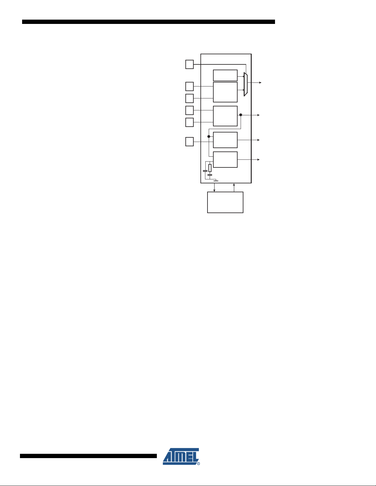
Figure 9-2. Clock Generator Block Diagram
AT91SAM9260
9.5 Power Management Controller
•Provides:
– the Processor Clock PCK
– the Master Clock MCK, in particular to the Matrix and the memory interfaces
– the USB Device Clock UDPCK
– independent peripheral clocks, typically at the frequency of MCK
– 2 programmable clock outputs: PCK0, PCK1
• Five flexible operating modes:
– Normal Mode, processor and peripherals running at a programmable frequency
– Idle Mode, processor stopped waiting for an interrupt
– Slow Clock Mode, processor and peripherals running at low frequency
– Standby Mode, mix of Idle and Backup Mode, peripheral running at low frequency,
processor stopped waiting for an interrupt
– Backup Mode, Main Power Supplies off, VDDBU powered by a battery
OSC_SEL
XIN32
XOUT32
XIN
XOUT
PLLRCA
Clock Generator
On Chip
RC OSC
Slow Clock
Oscillator
Main
Oscillator
PLL and
Divider A
PLL and
Divider B
ControlStatus
Power
Management
Controller
Slow Clock
SLCK
Main Clock
MAINCK
PLLA Clock
PLLACK
PLLB Clock
PLLBCK
6221HS–ATARM–31-Jan-08
29

Figure 9-3. AT91SAM9260 Power Management Controller Block Diagram
Processor
Clock
Controller
SLCK
MAINCK
PLLACK
PLLBCK
Master Clock Controller
Prescaler
/1,/2,/4,...,/64
Divider
/1,/2,/4
Programmable Clock Controller
Idle Mode
Peripherals
Clock Controller
ON/OFF
PCK
int
MCK
periph_clk[..]
9.6 Periodic Interval Timer
• Includes a 20-bit Periodic Counter, with less than 1 µs accuracy
• Includes a 12-bit Interval Overlay Counter
• Real Time OS or Linux
9.7 Watchdog Timer
• 16-bit key-protected only-once-Programmable Counter
• Windowed, prevents the processor being in a dead-lock on the watchdog access
9.8 Real-time Timer
– Real-time Timer 32-bit free-running back-up Counter
– Integrates a 16-bit programmable prescaler running on slow clock
– Alarm Register capable of generating a wake-up of the system through the
Shutdown Controller
SLCK
MAINCK
PLLACK
PLLBCK
PLLBCK
®
/Windows CE® compliant tick generator
Prescaler
/1,/2,/4,...,/64
USB Clock Controller
Divider
/1,/2,/4
ON/OFF
ON/OFF
pck[..]
UDPCK
UHPCK
9.9 General-purpose Back-up Registers
• Four 32-bit backup general-purpose registers
9.10 Advanced Interrupt Controller
• Controls the interrupt lines (nIRQ and nFIQ) of the ARM Processor
• Thirty-two individually maskable and vectored interrupt sources
– Source 0 is reserved for the Fast Interrupt Input (FIQ)
– Source 1 is reserved for system peripherals (PIT, RTT, PMC, DBGU, etc.)
30
AT91SAM9260
6221HS–ATARM–31-Jan-08

AT91SAM9260
– Programmable Edge-triggered or Level-sensitive Internal Sources
– Programmable Positive/Negative Edge-triggered or High/Low Level-sensitive
• Three External Sources plus the Fast Interrupt signal
• 8-level Priority Controller
– Drives the Normal Interrupt of the processor
– Handles priority of the interrupt sources 1 to 31
– Higher priority interrupts can be served during service of lower priority interrupt
• Vectoring
– Optimizes Interrupt Service Routine Branch and Execution
– One 32-bit Vector Register per interrupt source
– Interrupt Vector Register reads the corresponding current Interrupt Vector
•Protect Mode
– Easy debugging by preventing automatic operations when protect models are
enabled
•Fast Forcing
– Permits redirecting any normal interrupt source on the Fast Interrupt of the
processor
9.11 Debug Unit
• Composed of two functions:
•Two-pin UART
• Debug Communication Channel Support
9.12 Chip Identification
• Chip ID: 0x019803A2
• JTAG ID: 0x05B1303F
• ARM926 TAP ID: 0x0792603F
–Two-pin UART
– Debug Communication Channel (DCC) support
– Implemented features are 100% compatible with the standard Atmel
– Independent receiver and transmitter with a common programmable Baud Rate
Generator
– Even, Odd, Mark or Space Parity Generation
– Parity, Framing and Overrun Error Detection
– Automatic Echo, Local Loopback and Remote Loopback Channel Modes
– Support for two PDC channels with connection to receiver and transmitter
– Offers visibility of and interrupt trigger from COMMRX and COMMTX signals from
the ARM Processor’s ICE Interface
®
USART
6221HS–ATARM–31-Jan-08
31

10. Peripherals
10.1 User Interface
10.2 Identifiers
The peripherals are mapped in the upper 256 Mbytes of the address space between the
addresses 0xFFFA 0000 and 0xFFFC FFFF. Each User Peripheral is allocated 16 Kbytes of
address space. A complete memory map is presented in Figure 8-1 on page 21.
Table 10-1 defines the Peripheral Identifiers of the AT91SAM9260. A peripheral identifier is
required for the control of the peripheral interrupt with the Advanced Interrupt Controller and for
the control of the peripheral clock with the Power Management Controller.
Table 10-1. AT91SAM9260 Peripheral Identifiers
Peripheral ID Peripheral Mnemonic Peripheral Name External Interrupt
0 AIC Advanced Interrupt Controller FIQ
1 SYSC System Controller Interrupt
2 PIOA Parallel I/O Controller A
3 PIOB Parallel I/O Controller B
4 PIOC Parallel I/O Controller C
5 ADC Analog to Digital Converter
6 US0 USART 0
7 US1 USART 1
8 US2 USART 2
9 MCI Multimedia Card Interface
10 UDP USB Device Port
11 TWI Two-wire Interface
12 SPI0 Serial Peripheral Interface 0
13 SPI1 Serial Peripheral Interface 1
14 SSC Synchronous Serial Controller
15 - Reserved
16 - Reserved
17 TC0 Timer/Counter 0
18 TC1 Timer/Counter 1
19 TC2 Timer/Counter 2
20 UHP USB Host Port
21 EMAC Ethernet MAC
22 ISI Image Sensor Interface
23 US3 USART 3
24 US4 USART 4
25 US5 USART 5
26 TC3 Timer/Counter 3
27 TC4 Timer/Counter 4
28 TC5 Timer/Counter 5
32
AT91SAM9260
6221HS–ATARM–31-Jan-08

AT91SAM9260
Table 10-1. AT91SAM9260 Peripheral Identifiers (Continued)
Peripheral ID Peripheral Mnemonic Peripheral Name External Interrupt
29 AIC Advanced Interrupt Controller IRQ0
30 AIC Advanced Interrupt Controller IRQ1
31 AIC Advanced Interrupt Controller IRQ2
Note: Setting AIC, SYSC, UHP, ADC and IRQ0-2 bits in the clock set/clear registers of the PMC has no effect. The ADC clock is auto-
matically started for the first conversion. In Sleep Mode the ADC clock is automatically stopped after each conversion.
10.2.1 Peripheral Interrupts and Clock Control
10.2.1.1 System Interrupt
The System Interrupt in Source 1 is the wired-OR of the interrupt signals coming from:
• the SDRAM Controller
• the Debug Unit
• the Periodic Interval Timer
• the Real-time Timer
• the Watchdog Timer
• the Reset Controller
• the Power Management Controller
The clock of these peripherals cannot be deactivated and Peripheral ID 1 can only be used
within the Advanced Interrupt Controller.
10.2.1.2 External Interrupts
All external interrupt signals, i.e., the Fast Interrupt signal FIQ or the Interrupt signals IRQ0 to
IRQ2, use a dedicated Peripheral ID. However, there is no clock control associated with these
peripheral IDs.
10.3 Peripheral Signal Multiplexing on I/O Lines
The AT91SAM9260 features 3 PIO controllers (PIOA, PIOB, PIOC) that multiplex the I/O lines of
the peripheral set.
Each PIO Controller controls up to 32 lines. Each line can be assigned to one of two peripheral
functions, A or B. Table 10-2 on page 34, Table 10-3 on page 35 and Table 10-4 on page 36
define how the I/O lines of the peripherals A and B are multiplexed on the PIO Controllers. The
two columns “Function” and “Comments” have been inserted in this table for the user’s own
comments; they may be used to track how pins are defined in an application.
Note that some peripheral functions which are output only might be duplicated within both
tables.
The column “Reset State” indicates whether the PIO Line resets in I/O mode or in peripheral
mode. If I/O appears, the PIO Line resets in input with the pull-up enabled, so that the device is
maintained in a static state as soon as the reset is released. As a result, the bit corresponding to
the PIO Line in the register PIO_PSR (Peripheral Status Register) resets low.
If a signal name appears in the “Reset State” column, the PIO Line is assigned to this function
and the corresponding bit in PIO_PSR resets high. This is the case of pins controlling memories,
in particular the address lines, which require the pin to be driven as soon as the reset is
released. Note that the pull-up resistor is also enabled in this case.
6221HS–ATARM–31-Jan-08
33

10.3.1 PIO Controller A Multiplexing
Table 10-2. Multiplexing on PIO Controller A
PIO Controller A Application Usage
I/O Line Peripheral A Peripheral B Comments Reset State Power Supply Function Comments
PA0 SPI0_MISO MCDB0 I/O VDDIOP0
PA1 SPI0_MOSI MCCDB I/O VDDIOP0
PA2 SPI0_SPCK I/O VDDIOP0
PA3 SPI0_NPCS0 MCDB3 I/O VDDIOP0
PA4 RTS2 MCDB2 I/O VDDIOP0
PA5 CTS2 MCDB1 I/O VDDIOP0
PA6 MCDA0 I/O VDDIOP0
PA7 MCCDA I/O VDDIOP0
PA8 MCCK I/O VDDIOP0
PA9 MCDA1 I/O VDDIOP0
PA10 MCDA2 ETX2 I/O VDDIOP0
PA11 MCDA3 ETX3 I/O VDDIOP0
PA12 ETX0 I/O VDDIOP0
PA13 ETX1 I/O VDDIOP0
PA14 ERX0 I/O VDDIOP0
PA15 ERX1 I/O VDDIOP0
PA16 ETXEN I/O VDDIOP0
PA17 ERXDV I/O VDDIOP0
PA18 ERXER I/O VDDIOP0
PA19 ETXCK I/O VDDIOP0
PA20 EMDC I/O VDDIOP0
PA21 EMDIO I/O VDDIOP0
PA22 ADTRG ETXER I/O VDDIOP0
PA23 TWD ETX2 I/O VDDIOP0
PA24 TWCK ETX3 I/O VDDIOP0
PA25 TCLK0 ERX2 I/O VDDIOP0
PA26 TIOA0 ERX3 I/O VDDIOP0
PA27 TIOA1 ERXCK I/O VDDIOP0
PA28 TIOA2 ECRS I/O VDDIOP0
PA29 SCK1 ECOL I/O VDDIOP0
(1)
PA 30
(1)
PA 31
Note: 1. Not available in the 208-lead PQFP package.
SCK2 RXD4 I/O VDDIOP0
SCK0 TXD4 I/O VDDIOP0
34
AT91SAM9260
6221HS–ATARM–31-Jan-08

AT91SAM9260
10.3.2 PIO Controller B Multiplexing
Table 10-3. Multiplexing on PIO Controller B
PIO Controller B Application Usage
I/O Line Peripheral A Peripheral B Comments Reset State Power Supply Function Comments
PB0 SPI1_MISO TIOA3 I/O VDDIOP0
PB1 SPI1_MOSI TIOB3 I/O VDDIOP0
PB2 SPI1_SPCK TIOA4 I/O VDDIOP0
PB3 SPI1_NPCS0 TIOA5 I/O VDDIOP0
PB4 TXD0 I/O VDDIOP0
PB5 RXD0 I/O VDDIOP0
PB6 TXD1 TCLK1 I/O VDDIOP0
PB7 RXD1 TCLK2 I/O VDDIOP0
PB8 TXD2 I/O VDDIOP0
PB9 RXD2 I/O VDDIOP0
PB10 TXD3 ISI_D8 I/O VDDIOP1
PB11 RXD3 ISI_D9 I/O VDDIOP1
(1)
PB12
PB13
PB14 DRXD I/O VDDIOP0
PB15 DTXD I/O VDDIOP0
TXD5 ISI_D10 I/O VDDIOP1
(1)
RXD5 ISI_D11 I/O VDDIOP1
PB16 TK0 TCLK3 I/O VDDIOP0
PB17 TF0 TCLK4 I/O VDDIOP0
PB18 TD0 TIOB4 I/O VDDIOP0
PB19 RD0 TIOB5 I/O VDDIOP0
PB20 RK0 ISI_D0 I/O VDDIOP1
PB21 RF0 ISI_D1 I/O VDDIOP1
PB22 DSR0 ISI_D2 I/O VDDIOP1
PB23 DCD0 ISI_D3 I/O VDDIOP1
PB24 DTR0 ISI_D4 I/O VDDIOP1
PB25 RI0 ISI_D5 I/O VDDIOP1
PB26 RTS0 ISI_D6 I/O VDDIOP1
PB27 CTS0 ISI_D7 I/O VDDIOP1
PB28 RTS1 ISI_PCK I/O VDDIOP1
PB29 CTS1 ISI_VSYNC I/O VDDIOP1
PB30 PCK0 ISI_HSYNC I/O VDDIOP1
PB31 PCK1 ISI_MCK I/O VDDIOP1
Note: 1. Not available in the 208-lead PQFP package.
6221HS–ATARM–31-Jan-08
35

10.3.3 PIO Controller C Multiplexing
Table 10-4. Multiplexing on PIO Controller C
PIO Controller C Application Usage
I/O Line Peripheral A Peripheral B Comments Reset State Power Supply Function Comments
PC0 SCK3 AD0 I/O VDDANA
PC1 PCK0 AD1 I/O VDDANA
(1)
PC2
(1)
PC3
PC4 A23 SPI1_NPCS2 A23 VDDIOM
PC5 A24 SPI1_NPCS1 A24 VDDIOM
PC6 TIOB2 CFCE1 I/O VDDIOM
PC7 TIOB1 CFCE2 I/O VDDIOM
PC8 NCS4/CFCS0 RTS3 I/O VDDIOM
PC9 NCS5/CFCS1 TIOB0 I/O VDDIOM
PC10 A25/CFRNW CTS3 A25 VDDIOM
PC11 NCS2 SPI0_NPCS1 I/O VDDIOM
(1)
PC12
IRQ0 NCS7 I/O VDDIOM
PCK1 AD2 I/O VDDANA
SPI1_NPCS3 AD3 I/O VDDANA
PC13 FIQ NCS6 I/O VDDIOM
PC14 NCS3/NANDCS IRQ2 I/O VDDIOM
PC15 NWAIT IRQ1 I/O VDDIOM
PC16 D16 SPI0_NPCS2 I/O VDDIOM
PC17 D17 SPI0_NPCS3 I/O VDDIOM
PC18 D18 SPI1_NPCS1 I/O VDDIOM
PC19 D19 SPI1_NPCS2 I/O VDDIOM
PC20 D20 SPI1_NPCS3 I/O VDDIOM
PC21 D21 EF100 I/O VDDIOM
PC22 D22 TCLK5 I/O VDDIOM
PC23 D23 I/O VDDIOM
PC24 D24 I/O VDDIOM
PC25 D25 I/O VDDIOM
PC26 D26 I/O VDDIOM
PC27 D27 I/O VDDIOM
PC28 D28 I/O VDDIOM
PC29 D29 I/O VDDIOM
PC30 D30 I/O VDDIOM
PC31 D31 I/O VDDIOM
Note: 1. Not available in the 208-lead PQFP package.
36
AT91SAM9260
6221HS–ATARM–31-Jan-08

10.4 Embedded Peripherals
10.4.1 Serial Peripheral Interface
• Supports communication with serial external devices
– Four chip selects with external decoder support allow communication with up to 15
peripherals
– Serial memories, such as DataFlash and 3-wire EEPROMs
– Serial peripherals, such as ADCs, DACs, LCD Controllers, CAN Controllers and
Sensors
– External co-processors
• Master or slave serial peripheral bus interface
– 8- to 16-bit programmable data length per chip select
– Programmable phase and polarity per chip select
– Programmable transfer delays between consecutive transfers and between clock
and data per chip select
– Programmable delay between consecutive transfers
– Selectable mode fault detection
• Very fast transfers supported
– Transfers with baud rates up to MCK
– The chip select line may be left active to speed up transfers on the same device
AT91SAM9260
10.4.2 Two-wire Interface
• Master, MultiMaster and Slave modes supported
• General Call supported in Slave mode
10.4.3 USART
• Programmable Baud Rate Generator
• 5- to 9-bit full-duplex synchronous or asynchronous serial communications
• RS485 with driver control signal
• ISO7816, T = 0 or T = 1 Protocols for interfacing with smart cards
• IrDA modulation and demodulation
– 1, 1.5 or 2 stop bits in Asynchronous Mode or 1 or 2 stop bits in Synchronous Mode
– Parity generation and error detection
– Framing error detection, overrun error detection
– MSB- or LSB-first
– Optional break generation and detection
– By 8 or by-16 over-sampling receiver frequency
– Hardware handshaking RTS-CTS
– Optional modem signal management DTR-DSR-DCD-RI
– Receiver time-out and transmitter timeguard
– Optional Multi-drop Mode with address generation and detection
– NACK handling, error counter with repetition and iteration limit
6221HS–ATARM–31-Jan-08
37

– Communication at up to 115.2 Kbps
• Test Modes
– Remote Loopback, Local Loopback, Automatic Echo
The USART contains features allowing management of the Modem Signals DTR, DSR, DCD
and RI. In the AT91SAM9260, only the USART0 implements these signals, named DTR0,
DSR0, DCD0 and RI0.
The USART1 and USART2 do not implement all the modem signals. Only RTS and CTS (RTS1
and CTS1, RTS2 and CTS2, respectively) are implemented in these USARTs for other features.
Thus, programming the USART1, USART2 or the USART3 in Modem Mode may lead to unpredictable results. In these USARTs, the commands relating to the Modem Mode have no effect
and the status bits relating the status of the modem signals are never activated.
10.4.4 Serial Synchronous Controller
• Provides serial synchronous communication links used in audio and telecom applications
(with CODECs in Master or Slave Modes, I
• Contains an independent receiver and transmitter and a common clock divider
• Offers a configurable frame sync and data length
• Receiver and transmitter can be programmed to start automatically or on detection of
different event on the frame sync signal
• Receiver and transmitter include a data signal, a clock signal and a frame synchronization
signal
2
S, TDM Buses, Magnetic Card Reader, etc.)
10.4.5 Timer Counter
• Two blocks of three 16-bit Timer Counter channels
• Each channel can be individually programmed to perfom a wide range of functions including:
– Frequency Measurement
– Event Counting
– Interval Measurement
– Pulse Generation
–Delay Timing
– Pulse Width Modulation
– Up/down Capabilities
• Each channel is user-configurable and contains:
– Three external clock inputs
– Five internal clock inputs
– Two multi-purpose input/output signals
• Each block contains two global registers that act on all three TC Channels
Note: TC Block 0 (TC0, TC1, TC2) and TC Block 1 (TC3, TC4, TC5) have identical user interfaces. See
Figure 8-1, “AT91SAM9260 Memory Mapping,” on page 21 for TC Block 0 and TC Block 1
base addresses.
10.4.6 Multimedia Card Interface
• One double-channel MultiMedia Card Interface
• Compatibility with MultiMedia Card Specification Version 3.11
38
AT91SAM9260
6221HS–ATARM–31-Jan-08

10.4.7 USB Host Port
AT91SAM9260
• Compatibility with SD Memory Card Specification Version 1.1
• Compatibility with SDIO Specification Version V1.0.
• Card clock rate up to Master Clock divided by 2
• Embedded power management to slow down clock rate when not used
• MCI has two slots, each supporting
– One slot for one MultiMediaCard bus (up to 30 cards) or
– One SD Memory Card
• Support for stream, block and multi-block data read and write
• Compliance with Open HCI Rev 1.0 Specification
• Compliance with USB V2.0 Full-speed and Low-speed Specification
• Supports both Low-Speed 1.5 Mbps and Full-speed 12 Mbps devices
• Root hub integrated with two downstream USB ports in the 217-LFBGA package
• Two embedded USB transceivers
• Supports power management
• Operates as a master on the Matrix
10.4.8 USB Device Port
• USB V2.0 full-speed compliant, 12 MBits per second
• Embedded USB V2.0 full-speed transceiver
• Embedded 2,432-byte dual-port RAM for endpoints
• Suspend/Resume logic
• Ping-pong mode (two memory banks) for isochronous and bulk endpoints
• Six general-purpose endpoints
• Embedded pad pull-up
10.4.9 Ethernet 10/100 MAC
• Compatibility with IEEE Standard 802.3
• 10 and 100 MBits per second data throughput capability
• Full- and half-duplex operations
• MII or RMII interface to the physical layer
• Register Interface to address, data, status and control registers
• DMA Interface, operating as a master on the Memory Controller
• Interrupt generation to signal receive and transmit completion
• 28-byte transmit and 28-byte receive FIFOs
• Automatic pad and CRC generation on transmitted frames
• Address checking logic to recognize four 48-bit addresses
• Support promiscuous mode where all valid frames are copied to memory
– Endpoint 0 and 3: 64 bytes, no ping-pong mode
– Endpoint 1 and 2: 64 bytes, ping-pong mode
– Endpoint 4 and 5: 512 bytes, ping-pong mode
6221HS–ATARM–31-Jan-08
39

• Support physical layer management through MDIO interface
10.4.10 Image Sensor Interface
• ITU-R BT. 601/656 8-bit mode external interface support
• Support for ITU-R BT.656-4 SAV and EAV synchronization
• Vertical and horizontal resolutions up to 2048 x 2048
• Preview Path up to 640*480
• Support for packed data formatting for YCbCr 4:2:2 formats
• Preview scaler to generate smaller size image
• Programmable frame capture rate
10.4.11 Analog-to-Digital Converter
• 4-channel ADC
• 10-bit 312K samples/sec. Successive Approximation Register ADC
• -2/+2 LSB Integral Non Linearity, -1/+1 LSB Differential Non Linearity
• Individual enable and disable of each channel
• External voltage reference for better accuracy on low voltage inputs
• Multiple trigger source – Hardware or software trigger – External trigger pin – Timer Counter
0 to 2 outputs TIOA0 to TIOA2 trigger
• Sleep Mode and conversion sequencer – Automatic wakeup on trigger and back to sleep
mode after conversions of all enabled channels
• Four analog inputs shared with digital signals
40
AT91SAM9260
6221HS–ATARM–31-Jan-08

11. AT91SAM9260 Mechanical Characteristics
11.1 Package Drawings
Figure 11-1. 217-ball LFBGA Package Drawing
AT91SAM9260
Table 11-1. Soldering Informations
Ball Land 0.43 mm +/- 0.05
Soldering Mask Opening 0.30 mm +/- 0.05
Table 11-2. Device and 217-ball LFBGA Package Maximum Weight
450 mg
Table 11-3. 217-ball LFBGA Package Characteristics
Moisture Sensitivity Level 3
Table 11-4. Package Reference
JEDEC Drawing Reference MO-205
JESD97 Classification e1
6221HS–ATARM–31-Jan-08
41

Figure 11-2. 208-lead PQFP Package Drawing
Table 11-5. Device and 208-lead PQFP Package Maximum Weight
5.5 g
Table 11-6. 208-lead PQFP Package Characteristics
Moisture Sensitivity Level 3
Table 11-7. Package Reference
JEDEC Drawing Reference MS-022
JESD97 Classification e3
42
AT91SAM9260
6221HS–ATARM–31-Jan-08

11.2 Soldering Profile
Table 11-8 gives the recommended soldering profile from J-STD-20.
Table 11-8. Soldering Profile
Profile Feature PQFP208 Green Package
Average Ramp-up Rate (217°C to Peak) 3°C/sec. max. 3°C/sec. max.
Preheat Temperature 175°C ±25°C 180 sec. max. 180 sec. max.
Temperature Maintained Above 217°C 60 sec. to 150 sec. 60 sec. to 150 sec.
Time within 5°C of Actual Peak Temperature 20 sec. to 40 sec. 20 sec. to 40 sec.
Peak Temperature Range 260 +0 °C 260 +0 °C
Ramp-down Rate 6°C/sec. max. 6°C/sec. max.
Time 25°C to Peak Temperature 8 min. max. 8 min. max.
Note: It is recommended to apply a soldering temperature higher than 250°C
A maximum of three reflow passes is allowed per component.
AT91SAM9260
BGA217 Green
Package
6221HS–ATARM–31-Jan-08
43

12. AT91SAM9260 Ordering Information
Table 12-1. AT91SAM9260 Ordering Information
Ordering Code Package Package Type Temperature Operating Range
AT91SAM9260-QU PQFP208 Green
AT91SAM9260-CU BGA217 Green
Industrial
-40°C to 85°C
44
AT91SAM9260
6221HS–ATARM–31-Jan-08

AT91SAM9260
13. Revision History
Table 13-1. Revision History - current version appears first
Change Request
Revision Comments
6221HS
6221GS Updated all references to 217-ball LFBGA to Green package. Review
”Power Considerations”,in Section 5.1 ”Power Supplies”, VDDCORE and
VDDBU startup voltage restraints removed.
In Section 5.1 “Power Supplies” on page 14, VDDCORE and VDDBU, added
information on supply voltage during startup.
In Section 6.5 “I/O Line Drive Levels” on page 16, added information on PC4 to PC31. Review
In Section 6.7 “Slow Clock Selection” on page 16, corrected startup delay for internal
RC oscillator.
In Section 10.4.6 “Multimedia Card Interface” on page 38, corrected specification
version compatibility.
Ref.
5229
Review
Review
4944
6221FS
6221ES
In Section 8.1.1 “Boot Strategies” on page 22, removed sentence “When REMAP = 1,
BMS is ignored.”
Changed divider value for Master Clock Controller in Figure 9-3, ”AT91SAM9260
Power Management Controller Block Diagram” on page 30.
Corrected package reference to PQFP in
Drawing,” on page 42
Updated BGA ordering code in Section 43. ”AT91SAM9260 Ordering Information” on
page 780.
All new information in Section 7.2.1 ”Matrix Masters”, Table 7-1, “List of Bus Matrix
Masters,” on page 18 and Section 7.2.3 ”Master to Slave Access”, Table 7-3,
“AT91SAM9260 Masters to Slaves Access,” on page 18.
In Figure 2-1 ”AT91SAM9260 Block Diagram” on page 4, updated EBI signals NRD,
NWR0, NWR1, NWR3.
Added details on Timer/Counter blocks in Section 10.4.5 ”Timer Counter” on page 38.4369
Updated Chip ID in Section 9.12 ”Chip Identification” on page 32. 4582
Updated information on programmable pull-up resistor in
.
Figure 11-2, “208-lead PQFP Package
Section 6.4 ”PIO
Controllers” on page 16.
Updated
In
on clocking and corrected Peripheral Name for PID12, PID13 and PID14.
Placed comment on RDY/BUSY with PC13 in
Controller C,” on page 36
Section 6.7 ”Slow Clock Selection” on page 16.
Table 10-1, “AT91SAM9260 Peripheral Identifiers,” on page 32, added Note
Table 10-4, “Multiplexing on PIO
.
5026
4833
4740
4768
4457
4431
3972
3504 and 3543
3406
6221HS–ATARM–31-Jan-08
45

Table 13-1. Revision History - current version appears first
Revision Comments
Change Request
Ref.
6221DS
6221CS
Removed references to VDDOSC in
List”
, and in Section 5.1 ”Power Supplies” on page 14. Corrected VDDPLLA and
VDDPLLB with VDDPLL and GNDPLLA and GNDPLLB with GNDPLL in Table 4-1,
“Pinout for 208-pin PQFP Package,” on page 11
217-ball LFBGA Package,” on page 13
In
Figure 2-1 on page 4, corrected range for SCKx pins; label change on matrix
block.
Figure 2-1 on page 4 and Section 7.3 ”Peripheral DMA Controller” on page
In
19
, removed TWI PDC channels.
Section 6.3 ”Reset Pins” on page 15, added NRST as bidirectional. 3236
In
Figure 9-3 on page 30, added UHPCK as USB Clock Controller output. 3237
In
In
Section 10.4.3 ”USART” on page 37, added information on modem signals. 3245
For VDDIOP1, added supported voltage levels in
List,” on page 5
and corrected supported voltage levels in Section 5.2 ”Power
Consumption” on page 14
Removed package marking and updated package outline information in
”Package and Pinout” on page 10
Change to signal name for pin 147 in
Package” on page 11
Inserted new voltage information for JTAGSEL signal in
Description List”
In Table 3-1, “Signal Description List,” on page 5, added new voltage information for
OSCSEL and TST pins.
.
and in Section 6.1 ”JTAG Port Pins” on page 15.
“Features” , in Table 3-1, “Signal Description
and in Table 4-2, “Pinout for
.
Table 3-1, “Signal Description
.
Section 4.
.
Section 4-1 ”Pinout for 208-pin PQFP
Table 3-1, “Signal
3183
3235, 3071
3066
2874
2922
2907
2947
2979
In Section 6.3 ”Reset Pins” on page 15, new information on NRST and NRTST pins. 3003
Corrected ADC features in
page 40
Power consumption figures updated with current values in
6221BS
Consumption” on page 14.
Change to signal name for pin 47 in
Package” on page 11.
6221AS First issue.
Section 10.4.11 ”Analog-to-Digital Converter” on
.
2923
Section 5.2 ”Power
Section 4-1 ”Pinout for 208-pin PQFP
2843
46
AT91SAM9260
6221HS–ATARM–31-Jan-08
 Loading...