

NAND Flash Support in AT91SAM9
Microcontrollers
1. Scope
The purpose of this application note is to introduce the NAND Flash technology and to
describe how to interface NAND Flash memory to Atmel
based Microcontrollers that do not feature a NAND Flash Controller. The NAND Flash
logic is driven by the Static Memory Controller on the NCS3 address space.
Sample code is provided the associated zip file, Basic NAND Source Code.zip; the
source code is based on the product libV3.
2. NAND Flash Overview
2.1 General Overview
NAND Flash provides a cost effective alternative to hard drives, especially for portable
and handheld systems. The performance, pricing, and memory size options make it
optimal for storage applications
(pictures, audio files, etc.).
®
AT91SAM9 ARM® Thumb®-
AT91 ARM
Thumb
Microcontrollers
Application
Note
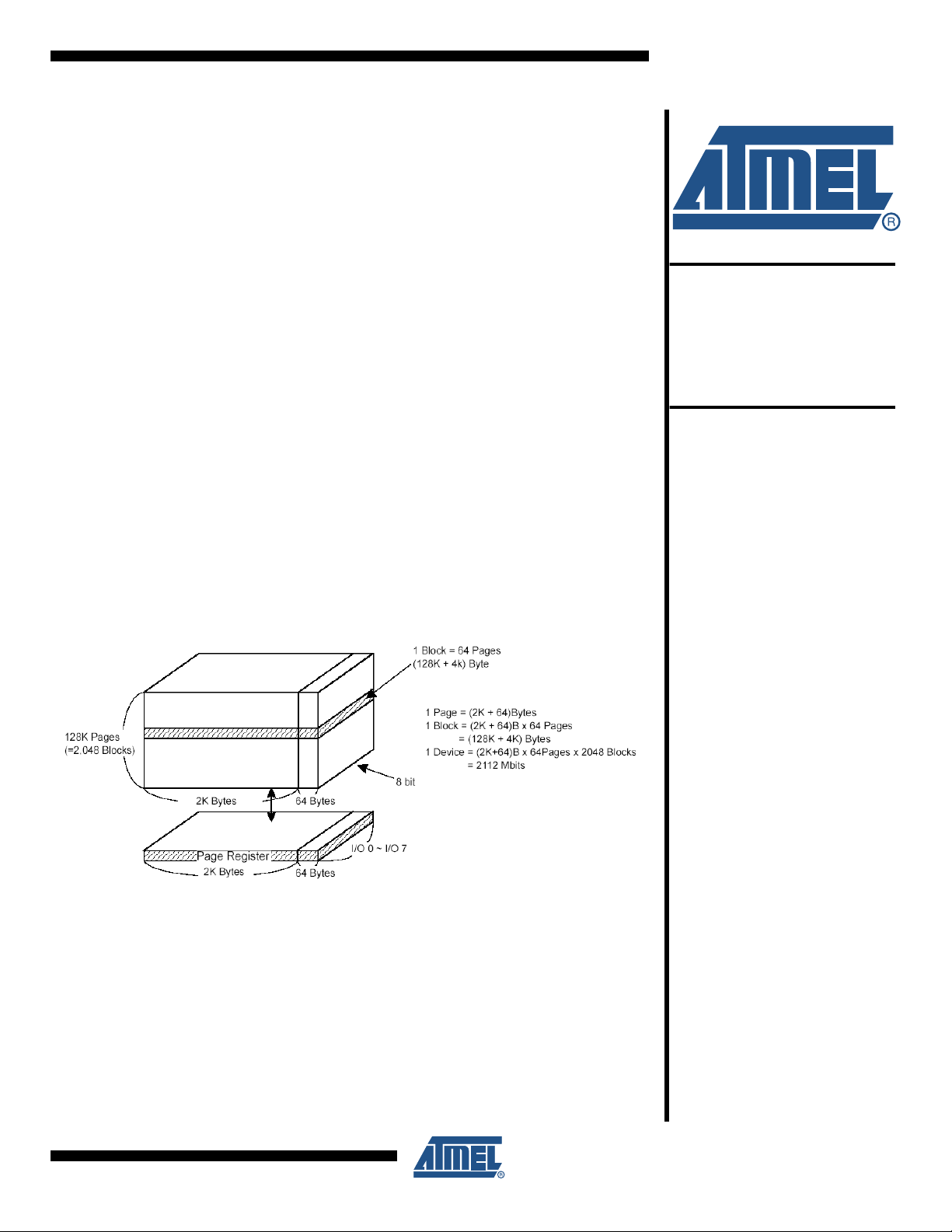
The NAND Flash used to illustrate this interface is the K9F2G08U0M, manufactured
by Samsung
Figure 2-1. K9F2G08U0M Organization
®
Electronics. Figure 2-1 shows the memory organization of this device.
6255B–ATARM–26-Jun-09

2.2 NAND Flash vs. NOR Flash
The most important item for memories is the cost per bit which depends on memory cell area per
bit. The cell area of NAND Flash is smaller than that of NOR Flash, making the NAND Flash
more cost effective than NOR Flash.
The first significant difference between NAND and NOR Flash is the hardware interface.
2.2.1 Hardware Interface
NOR Flash has a fully memory-mapped random access interface similar to a RAM, with dedicated address lines and data lines making it “bootable”.
NAND Flash uses a multiplexed I/O interface and additional control signals. It is controlled by
sending commands and addresses through an 8-bit or 16-bit bus to an internal command and
address register.
NOR Flash random-access interface typically composed of 41 pins:
– CE# - chip enable
– WE# - write enable
– OE# - output enable
– D[15:0] - data bus
– A[20:0] - address bus
– WP# - write protect
NAND Flash I/O device-type interface composed of up to 24 pins:
2.2.2 Array Architecture
NOR Flash is divided into blocks which typically contain many 16-bit wide words. Random
access to stored data words is achieved by placing the selected word address on the address
bus and then reading that data off the data bus. Erase operations are managed at the block level
and words can be programmed after a block has been erased.
NAND Flash is also divided into blocks which contain many pages instead of words (2K +64
bytes). Read and program operations take place on a per-page basis whereas erase operations
takes place on a block basis.
To read or write from NAND Flash, a command sequence is issued to select a block and a page.
After this selection, the entire page can be read or written.
– CE# - chip enable
– WE# - write enable
– RE# - read enable
– CLE - command latch enable
– ALE - address latch enable
– I/O[7:0] or I/O[15:0] - data bus
– WP# - write protect
– R/B# - ready / busy
– RE - Read enable
2
Application Note
6255B–ATARM–26-Jun-09
2.2.3 Performances
Application Note
NAND Flash typically contains blocks that contain errors and cannot be used. A check must be
done by software to list and maintain a table of bad blocks. Data integrity is achieved by using
hardware or software techniques, such as ECC, that check and correct bad data.
Further differences between NOR and NAND Flash can be found in read/write performances.
Table 2-1 shows random access time for NOR Flash specified at 0.09 µs, whereas NAND ran-
dom access is significantly slower — 25 µs — for the first byte. Once the initial access has been
made, however, the remaining 2,111 bytes are shifted out of NAND at only 30 ns per byte. This
results in a bandwidth of more than 23 Mb/s for 8-bit I/Os or 37 Mb/s for 16-bit I/Os.
The real benefits for NAND Flash can be found in the faster program and erase times, since
NAND provides over five megabytes per second of sustained write performance. The block
erase times are an impressive 2 ms for NAND versus 200 ms for NOR.
Table 2-1. Differences in Performance
2.2.4 Conclusion
NAND Flash
Characteristics
Random access read
Sustained read speed
(sector basis)
Random write speed 300 µs/2,112 bytes 20 µs / bytes
Sustained write speed (sector
basis)
Erase block size 128 Kbytes 64 Kbytes
Erase cycles 100,000 to 1,000,000 10,000 to 100,000
Erase time per block 2 ms 200 ms
K9F2G08U0M
25 µs (first byte)
30 ns each for remaining 2111
bytes
37 Mbytes/s 11 Mbytes/s
5 Mbytes/s 0.05 Mbytes/s
NOR Flash
AT49BV16x4-90
0.09 µs
Table 2-2 summarizes NAND/NOR advantages and disadvantages.
Table 2-2. NAND/NOR Comparison
NAND NOR
Fast writes
Advantages
Fast erases
Lower bit cost
Higher density
Random access
Byte writes possible
6255B–ATARM–26-Jun-09
Slow random access
Disadvantages
Applications
Byte writes difficult
Bad blocks management and ECC
required
File (disk) applications
Voice, data, video recorder
Any large sequential data
Slow writes
Slow erase
Execute directly from non volatile
memory
Clearly, NAND Flash has several significant positive attributes. The one negative attribute is that
it is not well-suited for direct random access.
3
NAND is available in large capacities and is the lowest cost Flash memory available today.
NAND is used in virtually all removable cards for cost/density reasons: USB Cards, Memory
Stick, MMC Multimedia Card, SD Secure Digital, CF Compact Flash.
3. Bad Block Management and Error Corrected Code (ECC)
3.1 Definition of “Bad Block”
By default, NAND devices contain invalid blocks which have one or more invalid bits.
Furthermore, since the first memory block (physical block address 00h) in NAND devices is
guaranteed to be free of defects (up to 1,000 PROGRAM/ERASE cycles), the first 8 Kb of Flash
memory can safely be used for system bootstrapping functions.
3.2 Software Considerations
To avoid writing to and reading from bad memory blocks, system software must create a map of
invalid memory blocks. If the application code executes from RAM rather than Flash memory,
system software bad-block mapping is only necessary at boot time and during Flash storage
updates.
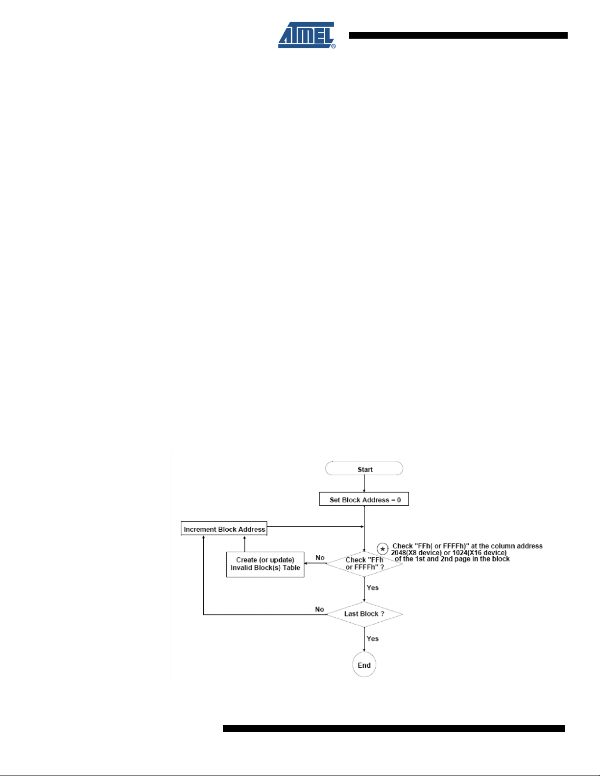
All device locations are erased (FFh for X8, FFFFh for X16) except locations where the invalid
block information is written prior to shipping. The invalid block status is defined by the 1st byte
(X8 device) or 1st word (X16 device) in the spare area.
The 1st or 2nd page of every invalid block has non-FFh(X8) or non-FFFFh(X16) data at the column address of 2048 (X8 device) or 1024 (X16 device). Since the invalid block information is
also erasable in most cases, it is impossible to recover the information once it has been erased.
Therefore, the system must be able to recognize the invalid block(s) based on the original invalid
block information and create the invalid block table via the flow chart in Figure 3-1.
Figure 3-1. Bad Block Recognition Flow Chart
4
Application Note
6255B–ATARM–26-Jun-09

Important Note: Any intentional erasure of the original invalid block information is prohibited.
3.3 ECC
NAND devices are subject to data failures that occur during device operation. To ensure data
read/write integrity, system error-checking and correction (ECC) algorithms must be implemented. Depending on the AT91 product, the ECC algorithm must be calculated by software or
can be generated by the embedded hardware ECC controller. The ECC controller is capable of
single bit error correction and 2-bit random detection. When NAND has more than 2 bits of
errors, the data cannot be corrected. This controller allows ECC management without CPU intervention and thus improves the total bandwidth of the system.
4. NAND Flash Signals
4.1 Bus Operation
The bus on NAND Flash devices is internally multiplexed. Data I/O, addresses, and commands
all share the same pins. I/O pins. I/O[15:8] are used only for data in the x16 configuration.
Addresses and commands are always supplied on I/O[7:0].
The command sequence normally consists of a command latch cycle, an ADDRESS LATCH
cycle, and a DATA cycle — either READ or WRITE.
Application Note
4.2 Control Signals
The signals CE#, WE#, RE#, CLE and ALE control Flash device READ and WRITE operations.
CE# is used to enable the device. When CE# is low and the device is not in the busy state, the
Flash memory accepts command, data, and address information.
When the device is not performing an operation, the CE# pin is typically driven HIGH and the
device enters standby mode. The memory enters standby if CE# goes HIGH while data is being
transferred and the device is not busy.
A subset of NAND Flash supports the CE# “Don’t Care” operation allowing the NAND Flash to
reside on the same asynchronous memory bus as other Flash or SRAM devices. Other devices
on the memory bus can then be accessed while the NAND Flash is busy with internal operations. This capability is important for designs that require multiple memory devices on the same
bus.
4.3 Commands (ALE = 0, CLE = 1)
All the NAND operations (except READ STATUS and RESET commands) consist of a command write cycle followed by address write cycle. The READ STATUS command does not have
an address write cycle. The command is transferred into the NAND command register followed
by the start address, for the read or program operation, latched into the address register.
Commands are written to the command register on the rising edge of WE# when:
• CE# and ALE are low
• CLE is high
Commands are input on I/O[7:0] only. For devices with a x16 interface, I/O[15:8] must be written
with zeros when issuing a command.
6255B–ATARM–26-Jun-09
5
4.4 Address (ALE = 1, CLE = 0)
Addresses are written to the address register on the rising edge of WE# when:
• CE# and CLE are low
• ALE is high
Addresses are input on I/O[7:0] only. For devices with a x16 interface, I/O[15:8] must be written
with zeros when issuing an address. Generally all five ADDRESS cycles are written to the
device.
4.5 Data (ALE = 0, CLE = 0)
Data is written to the data register on the rising edge of WE# when CE#, CLE, and ALE are low.
Data is input on I/O[7:0] for x8 devices, and I/O[15:0] on x16 devices.
4.6 Ready / Busy
The R/B# output provides a hardware method of indicating the completion of a PROGRAM/ERASE/READ operation. The signal is typically high, and transitions to low after the
appropriate command is written to the device. A dedicated PIO should be assigned to this signal
with a pull-up resistor for proper operation. Alternatively, the READ STATUS command can be
used by the software.
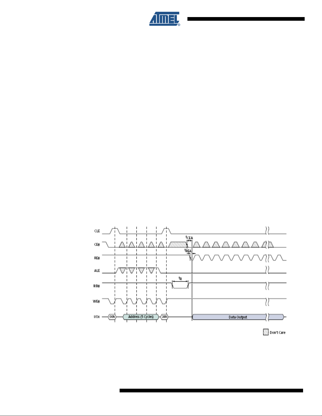
4.7 Example
The following waveforms shows the successive accesses: COMMAND Latch, ADDRESS Latch
and DATA Output with a “CE don’t Care” NAND. Notice that no command can be sent to the
NAND Flash during tR, because it is busy.
Figure 4-1. Page READ Operation
6
Application Note
6255B–ATARM–26-Jun-09
 Loading...