

Page 1

BDTIC www.bdtic.com/ATMEL
Features
• Incorporates the ARM7TDMI
– High-performance 32-bit RISC Architecture
– High-density 16-bit Instruction Set
– Leader in MIPS/Watt
– EmbeddedICE
• Internal High-speed Flash
– 512 Kbytes, Organized in Two Contiguous Banks of 1024 Pages of 256 Bytes Dual
Plane (AT91SAM7SE512)
– 256 Kbytes (AT91SAM7SE256) Organized in One Bank of 1024 Pages of 256 Bytes
Single Plane (AT91SAM7SE256)
– 32 Kbytes (AT91SAM7SE32) Organized in One Bank of 256 Pages of 128 Bytes
Single Plane (AT91SAM7SE32)
– Single Cycle Access at Up to 30 MHz in Worst Case Conditions
– Prefetch Buffer Optimizing Thumb Instruction Execution at Maximum Speed
– Page Programming Time: 6 ms, Including Page Auto-erase, Full Erase Time: 15 ms
– 10,000 Erase Cycles, 10-year Data Retention Capability, Sector Lock Capabilities,
Flash Security Bit
– Fast Flash Programming Interface for High Volume Production
• 32 Kbytes (AT91SAM7SE512/256) or 8 Kbytes (AT91SAM7SE32) of Internal
High-speed SRAM, Single-cycle Access at Maximum Speed
• One External Bus Interface (EBI)
– Supports SDRAM, Static Memory, Glueless Connection to CompactFlash® and
ECC-enabled NAND Flash
• Memory Controller (MC)
– Embedded Flash Controller
– Memory Protection Unit
– Abort Status and Misalignment Detection
• Reset Controller (RSTC)
– Based on Power-on Reset Cells and Low-power Factory-calibrated Brownout
Detector
– Provides External Reset Signal Shaping and Reset Source Status
• Clock Generator (CKGR)
– Low-power RC Oscillator, 3 to 20 MHz On-chip Oscillator and One PLL
• Power Management Controller (PMC)
– Power Optimization Capabilities, Including Slow Clock Mode (Down to 500 Hz) and
Idle Mode
– Three Programmable External Clock Signals
• Advanced Interrupt Controller (AIC)
– Individually Maskable, Eight-level Priority, Vectored Interrupt Sources
– Two External Interrupt Sources and One Fast Interrupt Source, Spurious Interrupt
Protected
• Debug Unit (DBGU)
– Two-wire UART and Support for Debug Communication Channel interrupt,
Programmable ICE Access Prevention
• Periodic Interval Timer (PIT)
– 20-bit Programmable Counter plus 12-bit Interval Counter
• Windowed Watchdog (WDT)
– 12-bit key-protected Programmable Counter
– Provides Reset or Interrupt Signals to the System
™
In-circuit Emulation, Debug Communication Channel Support
®
ARM® Thumb® Processor
Product
Description
AT91SAM7SE512
AT91SAM7SE256
AT91SAM7SE32
Summary
Preliminary
NOTE: This is a summary document.
The complete document is available on
the Atmel website at www.atmel.com.
6222ES–ATARM–04-Jan-08
Page 2

– Counter May Be Stopped While the Processor is in Debug State or in Idle Mode
• Real-time Timer (RTT)
– 32-bit Free-running Counter with Alarm
– Runs Off the Internal RC Oscillator
• Three Parallel Input/Output Controllers (PIO)
– Eighty-eight Programmable I/O Lines Multiplexed with up to Two Peripheral I/Os
– Input Change Interrupt Capability on Each I/O Line
– Individually Programmable Open-drain, Pull-up Resistor and Synchronous Output
– Schmitt Trigger on All inputs
• Eleven Peripheral DMA Controller (PDC) Channels
• One USB 2.0 Full Speed (12 Mbits per second) Device Port
– On-chip Transceiver, Eight Endpoints, 2688-byte Configurable Integrated FIFOs
• One Synchronous Serial Controller (SSC)
– Independent Clock and Frame Sync Signals for Each Receiver and Transmitter
– I²S Analog Interface Support, Time Division Multiplex Support
– High-speed Continuous Data Stream Capabilities with 32-bit Data Transfer
• Two Universal Synchronous/Asynchronous Receiver Transmitters (USART)
– Individual Baud Rate Generator, IrDA® Infrared Modulation/Demodulation
– Support for ISO7816 T0/T1 Smart Card, Hardware Handshaking, RS485 Support
– Full Modem Line Support on USART1
• One Master/Slave Serial Peripheral Interfaces (SPI)
– 8- to 16-bit Programmable Data Length, Four External Peripheral Chip Selects
• One Three-channel 16-bit Timer/Counter (TC)
– Three External Clock Inputs, Two Multi-purpose I/O Pins per Channel
– Double PWM Generation, Capture/Waveform Mode, Up/Down Capability
• One Four-channel 16-bit PWM Controller (PWMC)
• One Two-wire Interface (TWI)
– Master, Multi-Master and Slave Mode Support, All Two-wire Atmel EEPROMs Supported
– General Call Supported in Slave Mode
• One 8-channel 10-bit Analog-to-Digital Converter, Four Channels Multiplexed with Digital I/Os
• SAM-BA
• IEEE
®
– Default Boot program
– Interface with SAM-BA Graphic User Interface
®
1149.1 JTAG Boundary Scan on All Digital Pins
• Four High-current Drive I/O lines, Up to 16 mA Each
• Power Supplies
– Embedded 1.8V Regulator, Drawing up to 100 mA for the Core and External Components
– 1.8V or 3,3V VDDIO I/O Lines Power Supply, Independent 3.3V VDDFLASH Flash Power Supply
– 1.8V VDDCORE Core Power Supply with Brownout Detector
• Fully Static Operation:
– Up to 55 MHz at 1.8V and 85°C Worst Case Conditions
– Up to 48 MHz at 1.65V and 85°C Worst Case Conditions
• Available in a 128-lead LQFP Green Package, or a 144-ball LFBGA RoHS-compliant Package
2
AT91SAM7SE512/256/32 Preliminary
6222ES–ATARM–04-Jan-08
Page 3
1. Description
AT91SAM7SE512/256/32 Preliminary Summary
Atmel's AT91SAM7SE Series is a member of its Smart ARM Microcontroller family based on the
32-bit ARM7
• AT91SAM7SE512 features a 512 Kbyte high-speed Flash and a 32 Kbyte SRAM.
• AT91SAM7SE256 features a 256 Kbyte high-speed Flash and a 32 Kbyte SRAM.
• AT91SAM7SE32 features a 32 Kbyte high-speed Flash and an 8 Kbyte SRAM.
It also embeds a large set of peripherals, including a USB 2.0 device, an External Bus Interface
(EBI), and a complete set of system functions minimizing the number of external components.
The EBI incorporates controllers for synchronous DRAM (SDRAM) and Static memories and
features specific circuitry facilitating the interface for NAND Flash, SmartMedia and
CompactFlash.
The device is an ideal migration path for 8/16-bit microcontroller users looking for additional performance, extended memory and higher levels of system integration.
The embedded Flash memory can be programmed in-system via the JTAG-ICE interface or via
a parallel interface on a production programmer prior to mounting. Built-in lock bits and a security bit protect the firmware from accidental overwrite and preserve its confidentiality.
™
RISC processor and high-speed Flash memory.
The AT91SAM7SE Series system controller includes a reset controller capable of managing the
power-on sequence of the microcontroller and the complete system. Correct device operation
can be monitored by a built-in brownout detector and a watchdog running off an integrated RC
oscillator.
By combining the ARM7TDMI processor with on-chip Flash and SRAM, and a wide range of
peripheral functions, including USART, SPI, External Bus Interface, Timer Counter, RTT and
Analog-to-Digital Converters on a monolithic chip, the AT91SAM7SE512/256/32 is a powerful
device that provides a flexible, cost-effective solution to many embedded control applications.
1.1 Configuration Summary of the AT91SAM7SE512, AT91SAM7SE256 and AT91SAM7SE32
The AT91SAM7SE512, AT91SAM7SE256 and AT91SAM7SE32 differ in memory sizes and
organization. Table 1-1 below summarizes the configurations for the three devices.
Table 1-1. Configuration Summary
Device Flash Size Flash Organization RAM Size
AT91SAM7SE512 512K bytes dual plane 32K bytes
AT91SAM7SE256 256K bytes single plane 32K bytes
AT91SAM7SE32 32K bytes single plane 8K bytes
6222ES–ATARM–04-Jan-08
3
Page 4
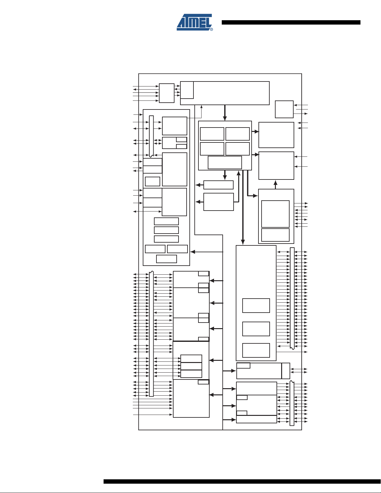
2. Block Diagram
Figure 2-1. AT91SAM7SE512/256/32 Block Diagram Signal Description
TDO
TMS
TCK
JTAGSEL
TST
IRQ0-IRQ1
DRXD
DTXD
PCK0-PCK2
PLLRC
XOUT
VDDFLASH
VDDCORE
VDDCORE
NRST
RXD0
TXD0
SCK0
RTS0
CTS0
RXD1
TXD1
SCK1
RTS1
CTS1
DCD1
DSR1
DTR1
NPCS0
NPCS1
NPCS2
NPCS3
MISO
MOSI
SPCK
TCLK0
TCLK1
TCLK2
TIOA0
TIOB0
TIOA1
TIOB1
TIOA2
TIOB2
ADTRG
AD0
AD1
AD2
AD3
AD4
AD5
AD6
AD7
ADVREF
TDI
FIQ
XIN
RI1
JTAG
SCAN
System Controller
PIO
DBGU
PLL
OSC
RCOSC
BOD
Controller
POR
PIT
WDT
RTT
PIOA
PIOB
PIO
AIC
PDC
PDC
PMC
Reset
PIOC
ICE
USART0
USART1
SPI
Timer Counter
TC0
TC1
TC2
ADC
ARM7TDMI
Processor
Memory Controller
Embedded
Flash
Controller
Abort
Status
Memory Protection
Peripheral Bridge
Peripheral DMA
Controller
11 Channels
APB
PDC
PDC
PDC
PDC
PDC
PDC
PDC
Address
Decoder
Misalignment
Detection
Unit
CompactFlash
NAND Flash
SDRAM
Controller
Static Memory
Controller
ECC
Controller
FIFO
USB Device
PWMC
PDC
PDC
SRAM
32 Kbytes (SE512/256)
8 Kbytes (SE32)
Flash
512 Kbytes (SE512)
256 Kbytes (SE256)
32 Kbytes (SE32)
ROM
Fast Flash
Programming
Interface
SAM-BA
EBI
SSC
TWI
1.8V
Voltage
Regulator
or
VDDIN
GND
VDDOUT
VDDCORE
VDDIO
VDDFLASH
ERASE
PGMRDY
PGMNVALID
PGMNOE
PGMCK
PGMM0-PGMM3
PGMD0-PGMD15
PGMNCMD
PGMEN0-PGMEN1
D[31:0]
A0/NBS0
A1/NBS2
A[15:2], A[20:18]
A21/NANDALE
A22/REG/NANDCLE
A16/BA0
A17/BA1
NCS0
NCS1/SDCS
NCS2/CFCS1
NCS3/NANDCS
NRD/CFOE
NWR0/NWE/CFWE
PIO
NWR1/NBS1/CFIOR
NBS3/CFIOW
SDCKE
RAS
CAS
SDWE
SDA10
CFRNW
NCS4/CFCS0
NCS5/CFCE1
NCS6/CFCE2
NCS7
NANDOE
NANDWE
NWAIT
SDCK
DDM
PIO
DDP
PWM0
PWM1
PWM2
PWM3
TF
TK
TD
RD
RK
RF
TWD
TWCK
Transciever
4
AT91SAM7SE512/256/32 Preliminary
6222ES–ATARM–04-Jan-08
Page 5

AT91SAM7SE512/256/32 Preliminary Summary
3. Signal Description
Table 3-1. Signal Description List
Active
Signal Name Function Type
Power
VDDIN
VDDOUT Voltage Regulator Output Power 1.85V
VDDFLASH Flash and USB Power Supply Power 3V to 3.6V
VDDIO I/O Lines Power Supply Power 3V to 3.6V or 1.65V to 1.95V
VDDCORE Core Power Supply Power 1.65V to 1.95V
VDDPLL PLL Power 1.65V to 1.95V
GND Ground Ground
XIN Main Oscillator Input Input
XOUT Main Oscillator Output Output
PLLRC PLL Filter Input
PCK0 - PCK2 Programmable Clock Output Output
TCK Test Clock Input No pull-up resistor
TDI Test Data In Input No pull-up resistor
TDO Test Data Out Output
TMS Test Mode Select Input No pull-up resistor.
JTAGSEL JTAG Selection Input Pull-down resistor
ERASE
NRST Microcontroller Reset I/O Low Open drain with pull-up resistor
TST Test Mode Select Input High Pull-down resistor
DRXD Debug Receive Data Input
DTXD Debug Transmit Data Output
IRQ0 - IRQ1 External Interrupt Inputs Input
FIQ Fast Interrupt Input Input
Voltage Regulator and ADC Power
Supply Input
Clocks, Oscillators and PLLs
ICE and JTAG
Flash Memory
Flash and NVM Configuration Bits Erase
Command
Reset/Test
Debug Unit
Power 3V to 3.6V
Input High Pull-down resistor
AIC
Level Comments
(1)
(1)
(1)
(1)
6222ES–ATARM–04-Jan-08
5
Page 6

Table 3-1. Signal Description List (Continued)
Active
Signal Name Function Type
PIO
PA0 - PA31 Parallel IO Controller A I/O Pulled-up input at reset
PB0 - PB31 Parallel IO Controller B I/O Pulled-up input at reset
PC0 - PC23 Parallel IO Controller C I/O Pulled-up input at reset
USB Device Port
DDM USB Device Port Data - Analog
DDP USB Device Port Data + Analog
USART
SCK0 - SCK1 Serial Clock I/O
TXD0 - TXD1 Transmit Data I/O
RXD0 - RXD1 Receive Data Input
RTS0 - RTS1 Request To Send Output
CTS0 - CTS1 Clear To Send Input
DCD1 Data Carrier Detect Input
DTR1 Data Terminal Ready Output
DSR1 Data Set Ready Input
RI1 Ring Indicator Input
Synchronous Serial Controller
TD Transmit Data Output
RD Receive Data Input
TK Transmit Clock I/O
RK Receive Clock I/O
TF Transmit Frame Sync I/O
RF Receive Frame Sync I/O
Timer/Counter
TCLK0 - TCLK2 External Clock Inputs Input
TIOA0 - TIOA2 Timer Counter I/O Line A I/O
TIOB0 - TIOB2 Timer Counter I/O Line B I/O
PWM Controller
PWM0 - PWM3 PWM Channels Output
Serial Peripheral Interface
MISO Master In Slave Out I/O
MOSI Master Out Slave In I/O
SPCK SPI Serial Clock I/O
NPCS0 SPI Peripheral Chip Select 0 I/O Low
NPCS1-NPCS3 SPI Peripheral Chip Select 1 to 3 Output Low
Level Comments
6
AT91SAM7SE512/256/32 Preliminary
6222ES–ATARM–04-Jan-08
Page 7

AT91SAM7SE512/256/32 Preliminary Summary
Table 3-1. Signal Description List (Continued)
Active
Signal Name Function Type
Two-Wire Interface
TWD Two-wire Serial Data I/O
TWCK Two-wire Serial Clock I/O
Analog-to-Digital Converter
AD0-AD3 Analog Inputs Analog Analog Inputs
AD4-AD7 Analog Inputs Analog Digital pulled-up inputs at reset
ADTRG ADC Trigger Input
ADVREF ADC Reference Analog
Fast Flash Programming Interface
PGMEN0-PGMEN2 Programming Enabling Input
PGMM0-PGMM3 Programming Mode Input
PGMD0-PGMD15 Programming Data I/O
PGMRDY Programming Ready Output High
PGMNVALID Data Direction Output Low
PGMNOE Programming Read Input Low
PGMCK Programming Clock Input
PGMNCMD Programming Command Input Low
External Bus Interface
D[31:0] Data Bus I/O
A[22:0] Address Bus Output
NWAIT External Wait Signal Input Low
Static Memory Controller
NCS[7:0] Chip Select Lines Output Low
NWR[1:0] Write Signals Output Low
NRD Read Signal Output Low
NWE Write Enable Output Low
NUB NUB: Upper Byte Select Output Low
NLB NLB: Lower Byte Select Output Low
EBI for CompactFlash Support
CFCE[2:1] CompactFlash Chip Enable Output Low
CFOE CompactFlash Output Enable Output Low
CFWE CompactFlash Write Enable Output Low
CFIOR CompactFlash I/O Read Signal Output Low
CFIOW CompactFlash I/O Write Signal Output Low
CFRNW CompactFlash Read Not Write Signal Output
CFCS[1:0] CompactFlash Chip Select Lines Output Low
Level Comments
6222ES–ATARM–04-Jan-08
7
Page 8

Table 3-1. Signal Description List (Continued)
Active
Signal Name Function Type
EBI for NAND Flash Support
NANDCS NAND Flash Chip Select Line Output Low
NANDOE NAND Flash Output Enable Output Low
NANDWE NAND Flash Write Enable Output Low
NANDCLE NAND Flash Command Line Enable Output Low
NANDALE NAND Flash Address Line Enable Output Low
SDRAM Controller
SDCK SDRAM Clock Output Tied low after reset
SDCKE SDRAM Clock Enable Output High
SDCS SDRAM Controller Chip Select Line Output Low
BA[1:0] Bank Select Output
SDWE SDRAM Write Enable Output Low
RAS - CAS Row and Column Signal Output Low
NBS[3:0] Byte Mask Signals Output Low
SDA10 SDRAM Address 10 Line Output
Note: 1. Refer to Section 6. “/O Lines Considerations” on page 15.
Level Comments
8
AT91SAM7SE512/256/32 Preliminary
6222ES–ATARM–04-Jan-08
Page 9
AT91SAM7SE512/256/32 Preliminary Summary
4. Package
The AT91SAM7SE512/256/32 is available in:
• 20 x 14 mm 128-lead LQFP package with a 0.5 mm lead pitch.
• 10x 10 x 1.4 mm 144-ball LFBGA package with a 0.8 mm lead pitch
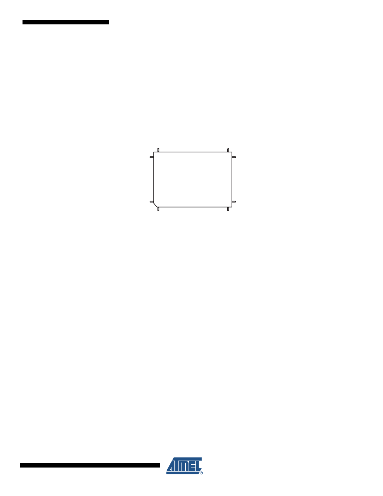
4.1 128-lead LQFP Package Outline
Figure 4-1 shows the orientation of the 128-lead LQFP package and a detailed mechanical
description is given in the Mechanical Characteristics section of the full datasheet.
Figure 4-1. 128-lead LQFP Package Outline (Top View)
103
128
102
1
65
64
39
38
6222ES–ATARM–04-Jan-08
9
Page 10

4.2 128-lead LQFP Pinout
Table 4-1. Pinout in 128-lead LQFP Package
1 ADVREF 33 PB31 65 TDI 97 SDCK
2 GND 34 PB30 66 TDO 98 PC8
3 AD7 35 PB29 67 PB2 99 PC7
4 AD6 36 PB28 68 PB1 100 PC6
5 AD5 37 PB27 69 PB0 101 PC5
6 AD4 38 PB26 70 GND 102 PC4
7 VDDOUT 39 PB25 71 VDDIO 103 PC3
8 VDDIN 40 PB24 72 VDDCORE 104 PC2
9 PA20/PGMD8/AD3 41 PB23 73 NRST 105 PC1
10 PA19/PGMD7/AD2 42 PB22 74 TST 106 PC0
11 PA18/PGMD6/AD1 43 PB21 75 ERASE 107 PA31
12 PA17/PGMD5/AD0 44 PB20 76 TCK 108 PA30
13 PA16/PGMD4 45 GND 77 TMS 109 PA29
14 PA15/PGMD3 46 VDDIO 78 JTAGSEL 110 PA28
15 PA14/PGMD2 47 VDDCORE 79 PC23 111 PA27/PGMD15
16 PA13/PGMD1 48 PB19 80 PC22 112 PA26/PGMD14
17 PA12/PGMD0 49 PB18 81 PC21 113 PA25/PGMD13
18 PA11/PGMM3 50 PB17 82 PC20 114 PA24/PGMD12
19 PA10/PGMM2 51 PB16 83 PC19 115 PA23/PGMD11
20 PA9/PGMM1 52 PB15 84 PC18 116 PA22/PGMD10
21 VDDIO 53 PB14 85 PC17 117 PA21/PGMD9
22 GND 54 PB13 86 PC16 118 VDDCORE
23 VDDCORE 55 PB12 87 PC15 119 GND
24 PA8/PGMM0 56 PB11 88 PC14 120 VDDIO
25 PA7/PGMNVALID 57 PB10 89 PC13 121 DM
26 PA6/PGMNOE 58 PB9 90 PC12 122 DP
27 PA5/PGMRDY 59 PB8 91 PC11 123 VDDFLASH
28 PA4/PGMNCMD 60 PB7 92 PC10 124 GND
29 PA3 61 PB6 93 PC9 125 XIN/PGMCK
30 PA2/PGMEN2 62 PB5 94 GND 126 XOUT
31 PA1/PGMEN1 63 PB4 95 VDDIO 127 PLLRC
32 PA0/PGMEN0 64 PB3 96 VDDCORE 128 VDDPLL
10
AT91SAM7SE512/256/32 Preliminary
6222ES–ATARM–04-Jan-08
Page 11
AT91SAM7SE512/256/32 Preliminary Summary
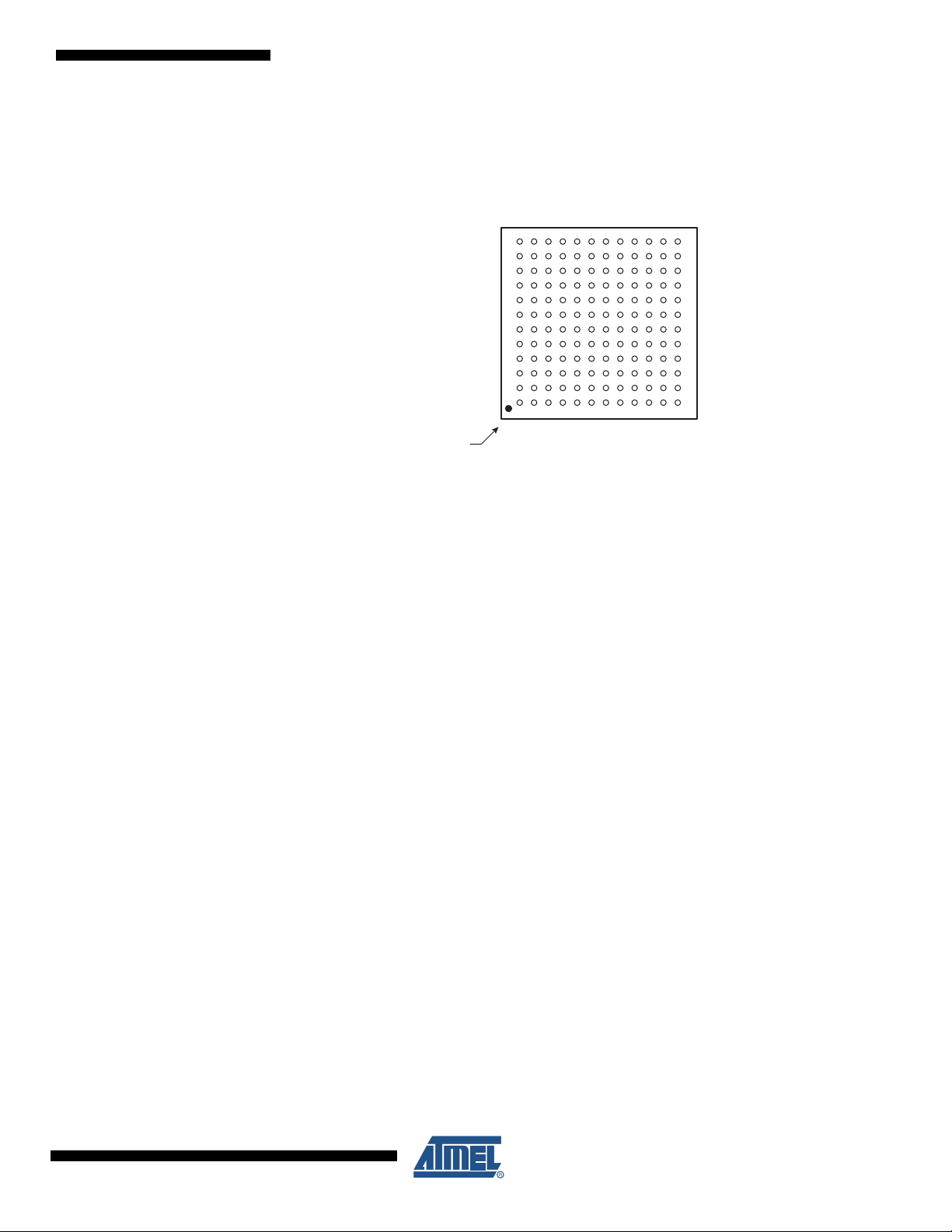
4.3 144-ball LFBGA Package Outline
Figure 4-2 shows the orientation of the 144-ball LFBGA package and a detailed mechanical
description is given in the Mechanical Characteristics section.
Figure 4-2. 144-ball LFBGA Package Outline (Top View)
Ball A1
12
11
10
9
8
7
6
5
4
3
2
1
ABCDEFGHJKLM
6222ES–ATARM–04-Jan-08
11
Page 12

4.4 144-ball LFBGA Pinout
Table 4-2. SAM7SE512/256/32 Pinout for 144-ball LFBGA Package
Pin Signal Name Pin Signal Name Pin Signal Name Pin Signal Name
A1 PB7 D1 VDDCORE G1 PC18 K1 PC11
A2 PB8 D2 VDDCORE G2 PC16 K2 PC6
A3 PB9 D3 PB2 G3 PC17 K3 PC2
A4 PB12 D4 TDO G4 PC9 K4 PC0
A5 PB13 D5 TDI G5 VDDIO K5 PA27/PGMD15
A6 PB16 D6 PB17 G6 GND K6 PA26/PGMD14
A7 PB22 D7 PB26 G7 GND K7 GND
A8 PB23 D8 PA14/PGMD2 G8 GND K8 VDDCORE
A9 PB25 D9 PA12/PGMD0 G9 GND K9 VDDFLASH
A10 PB29 D10 PA11/PGMM3 G10 AD4 K10 VDDIO
A11 PB30 D11 PA8/PGMM0 G11 VDDIN K11 VDDIO
A12 PB31 D12 PA7/PGMNVALID G12 VDDOUT K12 PA18/PGMD6/AD1
B1 PB6 E1 PC22 H1 PC15 L1 SDCK
B2 PB3 E2 PC23 H2 PC14 L2 PC7
B3 PB4 E3 NRST H3 PC13 L3 PC4
B4 PB10 E4 TCK H4 VDDCORE L4 PC1
B5 PB14 E5 ERASE H5 VDDCORE L5 PA29
B6 PB18 E6 TEST H6 GND L6 PA24/PGMD12
B7 PB20 E7 VDDCORE H7 GND L7 PA21/PGMD9
B8 PB24 E8 VDDCORE H8 GND L8 ADVREF
B9 PB28 E9 GND H9 GND L9 VDDFLASH
B10 PA4/PGMNCMD E10 PA9/PGMM1 H10 PA19/PGMD7/AD2 L10 VDDFLASH
B11 PA0/PGMEN0 E11 PA10/PGMM2 H11 PA20/PGMD8/AD3 L11 PA17/PGMD5/AD0
B12 PA1/PGMEN1 E12 PA13/PGMD1 H12 VDDIO L12 GND
C1 PB0 F1 PC21 J1 PC12 M1 PC8
C2 PB1 F2 PC20 J2 PC10 M2 PC5
C3 PB5 F3 PC19 J3 PA30 M3 PC3
C4 PB11 F4 JTAGSEL J4 PA28 M4 PA31
C5 PB15 F5 TMS J5 PA23/PGMD11 M5 PA25/PGMD13
C6 PB19 F6 VDDIO J6 PA22/PGMD10 M6 DM
C7 PB21 F7 GND J7 AD6 M7 DP
C8 PB27 F8 GND J8 AD7 M8 GND
C9 PA6/PGMNOE F9 GND J9 VDDCORE M9 XIN/PGMCK
C10 PA5/PGMRDY F10 AD5 J10 VDDCORE M10 XOUT
C11 PA2/PGMEN2 F11 PA15/PGMD3 J11 VDDCORE M11 PLLRC
C12 PA3 F12 PA16/PGMD4 J12 VDDIO M12 VDDPLL
12
AT91SAM7SE512/256/32 Preliminary
6222ES–ATARM–04-Jan-08
Page 13

AT91SAM7SE512/256/32 Preliminary Summary
5. Power Considerations
5.1 Power Supplies
The AT91SAM7SE512/256/32 has six types of power supply pins and integrates a voltage regulator, allowing the device to be supplied with only one voltage. The six power supply pin types
are:
• VDDIN pin. It powers the voltage regulator and the ADC; voltage ranges from 3.0V to 3.6V,
3.3V nominal.
• VDDOUT pin. It is the output of the 1.8V voltage regulator.
• VDDIO pin. It powers the I/O lines; two voltage ranges are supported:
– from 3.0V to 3.6V, 3.3V nominal
– or from 1.65V to 1.95V, 1.8V nominal.
• VDDFLASH pin. It powers the USB transceivers and a part of the Flash. It is required for the
Flash to operate correctly; voltage ranges from 3.0V to 3.6V, 3.3V nominal.
• VDDCORE pins. They power the logic of the device; voltage ranges from 1.65V to 1.95V,
1.8V typical. It can be connected to the VDDOUT pin with decoupling capacitor. VDDCORE
is required for the device, including its embedded Flash, to operate correctly.
• VDDPLL pin. It powers the oscillator and the PLL. It can be connected directly to the
VDDOUT pin.
In order to decrease current consumption, if the voltage regulator and the ADC are not used,
VDDIN, ADVREF, AD4, AD5, AD6 and AD7 should be connected to GND. In this case VDDOUT
should be left unconnected.
No separate ground pins are provided for the different power supplies. Only GND pins are provided and should be connected as shortly as possible to the system ground plane.
5.2 Power Consumption
The AT91SAM7SE512/256/32 has a static current of less than 60 µA on VDDCORE at 25°C,
including the RC oscillator, the voltage regulator and the power-on reset when the brownout
detector is deactivated. Activating the brownout detector adds 20 µA static current.
The dynamic power consumption on VDDCORE is less than 80 mA at full speed when running
out of the Flash. Under the same conditions, the power consumption on VDDFLASH does not
exceed 10 mA.
5.3 Voltage Regulator
The AT91SAM7SE512/256/32 embeds a voltage regulator that is managed by the System
Controller.
In Normal Mode, the voltage regulator consumes less than 100 µA static current and draws 100
mA of output current.
The voltage regulator also has a Low-power Mode. In this mode, it consumes less than 20 µA
static current and draws 1 mA of output current.
Adequate output supply decoupling is mandatory for VDDOUT to reduce ripple and avoid oscillations. The best way to achieve this is to use two capacitors in parallel:
6222ES–ATARM–04-Jan-08
13
Page 14
• One external 470 pF (or 1 nF) NPO capacitor should be connected between VDDOUT and
GND as close to the chip as possible.
• One external 2.2 µF (or 3.3 µF) X7R capacitor should be connected between VDDOUT and
GND.
Adequate input supply decoupling is mandatory for VDDIN in order to improve startup stability
and reduce source voltage drop. The input decoupling capacitor should be placed close to the
chip. For example, two capacitors can be used in parallel: 100 nF NPO and 4.7 µF X7R.
5.4 Typical Powering Schematics
The AT91SAM7SE512/256/32 supports a 3.3V single supply mode. The internal regulator input
connected to the 3.3V source and its output feeds VDDCORE and the VDDPLL. Figure 5-1
shows the power schematics to be used for USB bus-powered systems.
Figure 5-1. 3.3V System Single Power Supply Schematic
VDDFLASH
Power Source
ranges
from 4.5V (USB)
to 18V
DC/DC Converter
3.3V
VDDIO
VDDIN
VDDOUT
VDDCORE
VDDPLL
Voltage
Regulator
14
AT91SAM7SE512/256/32 Preliminary
6222ES–ATARM–04-Jan-08
Page 15

AT91SAM7SE512/256/32 Preliminary Summary
6. /O Lines Considerations
6.1 JTAG Port Pins
TMS, TDI and TCK are Schmitt trigger inputs. TMS, TDI and TCK do not integrate a pull-up
resistor.
TDO is an output, driven at up to VDDIO, and has no pull-up resistor.
The JTAGSEL pin is used to select the JTAG boundary scan when asserted at a high level. The
JTAGSEL pin integrates a permanent pull-down resistor of about 15 kΩ.
To eliminate any risk of spuriously entering the JTAG boundary scan mode due to noise on
JTAGSEL, it should be tied externally to GND if boundary scan is not used, or put in place an
external low value resistor (such as 1 kΩ).
6.2 Test Pin
The TST pin is used for manufacturing test or fast programming mode of the
AT91SAM7SE512/256/32 when asserted high. The TST pin integrates a permanent pull-down
resistor of about 15 kΩ to GND.
To eliminate any risk of entering the test mode due to noise on the TST pin, it should be tied to
GND if the FFPI is not used, or put in place an external low value resistor (such as 1 kΩ).
6.3 Reset Pin
6.4 ERASE Pin
To enter fast programming mode, the TST pin and the PA0 and PA1 pins should be tied high
and PA2 tied low.
Driving the TST pin at a high level while PA0 or PA1 is driven at 0 leads to unpredictable results.
The NRST pin is bidirectional with an open-drain output buffer. It is handled by the on-chip reset
controller and can be driven low to provide a reset signal to the external components or asserted
low externally to reset the microcontroller. There is no constraint on the length of the reset pulse,
and the reset controller can guarantee a minimum pulse length. This allows connection of a simple push-button on the NRST pin as system user reset, and the use of the NRST signal to reset
all the components of the system.
An external power-on reset can drive this pin during the start-up instead of using the internal
power-on reset circuit.
The NRST pin integrates a permanent pull-up of about 100 kΩ resistor to VDDIO.
This pin has Schmitt trigger input.
The ERASE pin is used to re-initialize the Flash content and some of its NVM bits. It integrates a
permanent pull-down resistor of about 15 kΩ to GND.
To eliminate any risk of erasing the Flash due to noise on the ERASE pin, it shoul be tied externally to GND, which prevents erasing the Flash from the applicatiion, or put in place an external
low value resistor (such as 1 kΩ).
6222ES–ATARM–04-Jan-08
This pin is debounced by the RC oscillator to improve the glitch tolerance. When the pin is tied to
high during less than 100 ms, ERASE pin is not taken into account. The pin must be tied high
during more than 220 ms to perform the re-initialization of the Flash.
15
Page 16

6.5 SDCK Pin
The SDCK pin is dedicated to the SDRAM Clock and is an output-only without pull-up. Maximum
Output Frequency of this pad is 48 MHz at 3.0V and 25 MHz at 1.65V with a maximum load of
30 pF.
6.6 PIO Controller lines
All the I/O lines PA0 to PA31, PB0 to PB31, PC0 to PC23 integrate a programmable pull-up
resistor. Programming of this pull-up resistor is performed independently for each I/O line
through the PIO controllers.
Typical pull-up value is 100 kΩ.
All the I/O lines have schmitt trigger inputs.
6.7 I/O Lines Current Drawing
The PIO lines PA0 to PA3 are high-drive current capable. Each of these I/O lines can drive up to
16 mA permanently.
The remaining I/O lines can draw only 8 mA.
However, the total current drawn by all the I/O lines cannot exceed 300 mA.
16
AT91SAM7SE512/256/32 Preliminary
6222ES–ATARM–04-Jan-08
Page 17

AT91SAM7SE512/256/32 Preliminary Summary
7. Processor and Architecture
7.1 ARM7TDMI Processor
• RISC processor based on ARMv4T Von Neumann architecture
– Runs at up to 55 MHz, providing 0.9 MIPS/MHz (core supplied with 1.8V)
• Two instruction sets
–ARM
–Thumb
• Three-stage pipeline architecture
– Instruction Fetch (F)
– Instruction
– Execute (E)
7.2 Debug and Test Features
• EmbeddedICE™ (Integrated embedded in-circuit emulator)
– Two watchpoint units
– Test access port accessible through a JTAG protocol
– Debug communication channel
• Debug Unit
–Two-pin UART
– Debug communication channel interrupt handling
– Chip ID Register
• IEEE1149.1 JTAG Boundary-scan on all digital pins
®
high-performance 32-bit instruction set
®
high code density 16-bit instruction set
Decode (D)
7.3 Memory Controller
• Programmable Bus Arbiter
• Address decoder provides selection signals for
• Abort Status Registers
• Misalignment Detector
• Remap Command
• 16-area Memory Protection Unit (Internal Memory and peripheral protection only)
– Handles requests from the ARM7TDMI and the Peripheral DMA Controller
– Four internal 1 Mbyte memory areas
– One 256-Mbyte embedded peripheral area
– Eight external 256-Mbyte memory areas
– Source, Type and all parameters of the access leading to an abort are saved
– Facilitates debug by detection of bad pointers
– Alignment checking of all data accesses
– Abort generation in case of misalignment
– Remaps the SRAM in place of the embedded non-volatile memory
– Allows handling of dynamic exception vectors
6222ES–ATARM–04-Jan-08
17
Page 18

– Individually programmable size between 1K Byte and 1M Byte
– Individually programmable protection against write and/or user access
– Peripheral protection against write and/or user access
• Embedded Flash Controller
– Embedded Flash interface, up to three programmable wait states
– Prefetch buffer, buffering and anticipating the 16-bit requests, reducing the required
wait states
– Key-protected program, erase and lock/unlock sequencer
– Single command for erasing, programming and locking operations
– Interrupt generation in case of forbidden operation
7.4 External Bus Interface
• Integrates Three External Memory Controllers:
– Static Memory Controller
– SDRAM Controller
– ECC Controller
• Additional Logic for NAND Flash and CompactFlash
– NAND Flash support: 8-bit as well as 16-bit devices are supported
– CompactFlash support: all modes (Attribute Memory, Common Memory, I/O, True
IDE) are supported but the signals _IOIS16 (I/O and True IDE modes) and -ATA SEL
(True IDE mode) are not handled.
• Optimized External Bus:
– 16- or 32-bit Data Bus (32-bit Data Bus for SDRAM only)
– Up to 23-bit Address Bus, Up to 8-Mbytes Addressable
– Up to 8 Chip Selects, each reserved to one of the eight Memory Areas
– Optimized pin multiplexing to reduce latencies on External Memories
• Configurable Chip Select Assignment:
– Static Memory Controller on NCS0
– SDRAM Controller or Static Memory Controller on NCS1
– Static Memory Controller on NCS2, Optional CompactFlash Support
– Static Memory Controller on NCS3, NCS5 - NCS6, Optional NAND Flash Support
– Static Memory Controller on NCS4, Optional CompactFlash Support
– Static Memory Controller on NCS7
®
Support
7.5 Static Memory Controller
• External memory mapping, 512-Mbyte address space
• 8-, or 16-bit Data Bus
• Up to 8 Chip Select Lines
• Multiple Access Modes supported
– Byte Write or Byte Select Lines
– Two different Read Protocols for each Memory Bank
18
AT91SAM7SE512/256/32 Preliminary
6222ES–ATARM–04-Jan-08
Page 19

• Multiple device adaptability
• Multiple Wait State Management
7.6 SDRAM Controller
• Numerous configurations supported
• Programming facilities
• Energy-saving capabilities
• Error detection
• SDRAM Power-up Initialization by software
• Latency is set to two clocks (CAS Latency of 1, 3 Not Supported)
• Auto Precharge Command not used
• Mobile SDRAM supported (except for low-power extended mode and deep power-down
mode)
AT91SAM7SE512/256/32 Preliminary Summary
– Compliant with LCD Module
– Compliant with PSRAM in synchronous operations
– Programmable Setup Time Read/Write
– Programmable Hold Time Read/Write
– Programmable Wait State Generation
– External Wait Request
– Programmable Data Float Time
– 2K, 4K, 8K Row Address Memory Parts
– SDRAM with two or four Internal Banks
– SDRAM with 16- or 32-bit Data Path
– Word, half-word, byte access
– Automatic page break when Memory Boundary has been reached
– Multibank Ping-pong Access
– Timing parameters specified by software
– Automatic refresh operation, refresh rate is programmable
– Self-refresh, and Low-power Modes supported
– Refresh Error Interrupt
7.7 Error Corrected Code Controller
• Tracking the accesses to a NAND Flash device by triggering on the corresponding chip select
• Single bit error correction and 2-bit Random detection.
• Automatic Hamming Code Calculation while writing
– ECC value available in a register
• Automatic Hamming Code Calculation while reading
– Error Report, including error flag, correctable error flag and word address being
detected erroneous
– Supports 8- or 16-bit NAND Flash devices with 512-, 1024-, 2048- or 4096-byte
pages
6222ES–ATARM–04-Jan-08
19
Page 20

7.8 Peripheral DMA Controller
• Handles data transfer between peripherals and memories
• Eleven channels
– Two for each USART
– Two for the Debug Unit
– Two for the Serial Synchronous Controller
– Two for the Serial Peripheral Interface
– One for the Analog-to-digital Converter
• Low bus arbitration overhead
– One Master Clock cycle needed for a transfer from memory to peripheral
– Two Master Clock cycles needed for a transfer from peripheral to memory
• Next Pointer management for reducing interrupt latency requirements
• Peripheral DMA Controller (PDC) priority is as follows (from the highest priority to the lowest):
Receive DBGU
Receive USART0
Receive USART1
Receive SSC
Receive ADC
Receive SPI
Tr an s m it D B GU
Transmit USART0
Transmit USART1
Transmit SSC
Transmit SPI
20
AT91SAM7SE512/256/32 Preliminary
6222ES–ATARM–04-Jan-08
Page 21

8. Memories
AT91SAM7SE512/256/32 Preliminary Summary
• 512 Kbytes of Flash Memory (AT91SAM7SE512)
– dual plane
– two contiguous banks of 1024 pages of 256 bytes
– Fast access time, 30 MHz single-cycle access in Worst Case conditions
– Page programming time: 6 ms, including page auto-erase
– Page programming without auto-erase: 3 ms
– Full chip erase time: 15 ms
– 10,000 write cycles, 10-year data retention capability
– 32 lock bits, each protecting 32 lock regions of 64 pages
– Protection Mode to secure contents of the Flash
• 256 Kbytes of Flash Memory (AT91SAM7SE256)
– single plane
– one bank of 1024 pages of 256 bytes
– Fast access time, 30 MHz single-cycle access in Worst Case conditions
– Page programming time: 6 ms, including page auto-erase
– Page programming without auto-erase: 3 ms
– Full chip erase time: 15 ms
– 10,000 cycles, 10-year data retention capability
– 16 lock bits, each protecting 16 lock regions of 64 pages
– Protection Mode to secure contents of the Flash
• 32 Kbytes of Flash Memory (AT91SAM7SE32)
– single plane
– one bank of 256 pages of 128 bytes
– Fast access time, 30 MHz single-cycle access in Worst Case conditions
– Page programming time: 6 ms, including page auto-erase
– Page programming without auto-erase: 3 ms
– Full chip erase time: 15 ms
– 10,000 cycles, 10-year data retention capability
– 8 lock bits, each protecting 8 lock regions of 32 pages
– Protection Mode to secure contents of the Flash
• 32 Kbytes of Fast SRAM (AT91SAM7SE512/256)
– Single-cycle access at full speed
• 8 Kbytes of Fast SRAM (AT91SAM7SE32)
– Single-cycle access at full speed
6222ES–ATARM–04-Jan-08
21
Page 22

Figure 8-1. AT91SAM7SE Memory Mapping
Address Memory Space Internal Memory Mapping
0x0000 0000
0x0FFF FFFF
0x1000 0000
0x1FFF FFFF
0x2000 0000
0x2FFF FFFF
0x3000 0000
0x3FFF FFFF
0x4000 0000
0x4FFF FFFF
0x5000 0000
0x5FFF FFFF
0x6000 0000
0x6FFF FFFF
0x7000 0000
0x7FFF FFFF
0x8000 0000
0x8FFF FFFF
0x9000 0000
0xEFFF FFFF
0xF000 0000
0xFFFF FFFF
Internal Memories
EBI
Chip Select 0
SMC
EBI
Chip Select 1
SMC or SDRAMC
EBI
Chip Select 2
SMC
Compact Flash
EBI
Chip Select 3
SMC/NANDFlash/
SmartMedia
EBI
Chip Select 4
SMC
Compact Flash
EBI
Chip Select 5
SMC
EBI
Chip Select 6
EBI
Chip Select 7
Undefined
(Abort)
Internal Peripherals
256 MBytes
256 MBytes
256 MBytes
256 MBytes
256 MBytes
256 MBytes
256 MBytes
256 MBytes
256 MBytes
6 x 256 MBytes
1,536 MBytes
256 MBytes
0xF000 0000
0xFFF9 FFFF
0xFFFA 0000
0xFFFA 3FFF
0xFFFA 4000
0xFFFA FFFF
0xFFFB 0000
0xFFFB 3FFF
0xFFFB 4000
0xFFFB 7FFF
0xFFFB 8000
0xFFFB BFFF
0xFFFB C000
0xFFFB FFFF
0xFFFC 0000
0xFFFC 3FFF
0xFFFC 4000
0xFFFC 7FFF
0xFFFC 8000
0xFFFC BFFF
0xFFFC C000
0xFFFC FFFF
0xFFFD 0000
0xFFFD 3FFF
0xFFFD 4000
0xFFFD 7FFF
0xFFFD 8000
0xFFFD BFFF
0xFFFD C000
0xFFFD FFFF
0xFFFE 0000
0xFFFE 3FFF
0xFFFE 4000
0xFFFF EFFF
0xFFFF F000
0xFFFF FFFF
0x0000 0000
0x000F FFFF
0x0010 0000
0x001F FFFF
0x0020 0000
0x002F FFFF
0x0030 0000
0x003F FFFF
0x0040 0000
0x0FFF FFFF
Peripheral Mapping
TC0, TC1, TC2
Boot Memory (1)
Flash before Remap
SRAM after Remap
Internal Flash
Internal SRAM
Internal ROM
Reserved
ReservedReserved
Reserved
UDP
Reserved
TWI
Reserved
USART0
USART1
ReservedReserved
PWMC
ReservedReserved
SSC
ADC
ReservedReserved
SPI
Reserved
SYSC
16 Kbytes
16 Kbytes
16 Kbytes
16 Kbytes
16 Kbytes
16 Kbytes
16 Kbytes
16 Kbytes
16 Kbytes
1 MBytes
1 MBytes
1 MBytes
1 MBytes
252 MBytes
Note:
(1) Can be ROM, Flash or SRAM
depending on GPNVM2 and REMAP
System Controller Mapping
0xFFFF F000
0xFFFF F1FF
0xFFFF F200
DBGU
0xFFFF F3FF
0xFFFF F400
PIOA
0xFFFF F5FF
0xFFFF F600
PIOB
0xFFFF F7FF
0xFFFF F800
PIOC
0xFFFF F9FF
0xFFFF FA00
Reserved
0xFFFF FBFF
0xFFFF FC00
0xFFFF FCFF
0xFFFF FD00
0xFFFF FD0F
0xFFFF FD20
0xFFFF FC2F
0xFFFF FD30
0xFFFF FC3F
0xFFFF FD40
0xFFFF FD4F
0xFFFF FD60
0xFFFF FC6F
0xFFFF FD70
0xFFFF FEFF
0xFFFF FF00
0xFFFF FFFF
PMC
RSTC
Reserved
WDT
Reserved
VREG
Reserved
AIC
RTT
PIT
MC
512 Bytes/128 registers
512 Bytes/128 registers
512 Bytes/128 registers
512 Bytes/128 registers
512 Bytes/128 registers
256 Bytes/64 registers
16 Bytes/4 registers
16 Bytes/4 registers
16 Bytes/4 registers
16 Bytes/4 registers
4 Bytes/1 register
256 Bytes/64 registers
22
AT91SAM7SE512/256/32 Preliminary
6222ES–ATARM–04-Jan-08
Page 23

AT91SAM7SE512/256/32 Preliminary Summary
A first level of address decoding is performed by the Memory Controller, i.e., by the implementation of the Advanced System Bus (ASB) with additional features.
Decoding splits the 4G bytes of address space into 16 areas of 256M bytes. The areas 1 to 8 are
directed to the EBI that associates these areas to the external chip selects NC0 to NCS7. The
area 0 is reserved for the addressing of the internal memories, and a second level of decoding
provides 1M byte of internal memory area. The area 15 is reserved for the peripherals and provides access to the Advanced Peripheral Bus (APB).
Other areas are unused and performing an access within them provides an abort to the master
requesting such an access.
8.1 Embedded Memories
8.1.1 Internal Memories
8.1.1.1 Internal SRAM
The AT91SAM7SE512/256 embeds a high-speed 32-Kbyte SRAM bank. The AT91SAM7SE32
embeds a high-speed 8-Kbyte SRAM bank. After reset and until the Remap Command is performed, the SRAM is only accessible at address 0x0020 0000. After Remap, the SRAM also
becomes available at address 0x0.
8.1.1.2 Internal ROM
8.1.1.3 Internal Flash
The AT91SAM7SE512/256/32 embeds an Internal ROM. At any time, the ROM is mapped at
address 0x30 0000. The ROM contains the FFPI and the SAM-BA boot program.
• The AT91SAM7SE512 features two banks of 256 Kbytes of Flash.
• The AT91SAM7SE256 features one bank of 256 Kbytes of Flash.
• The AT91SAM7SE32 features one bank of 32 Kbytes of Flash.
At any time, the Flash is mapped to address 0x0010 0000.
A general purpose NVM (GPNVM) bit is used to boot either on the ROM (default) or from the
Flash.
This GPNVM bit can be cleared or set respectively through the commands “Clear General-purpose NVM Bit” and “Set General-purpose NVM Bit” of the EFC User Interface.
Setting the GPNVM bit 2 selects the boot from the Flash, clearing it selects the boot from the
ROM. Asserting ERASE clears the GPNVM bit 2 and thus selects the boot from the ROM by
default.
6222ES–ATARM–04-Jan-08
23
Page 24

Figure 8-2. Internal Memory Mapping with GPNVM Bit 2 = 0 (default)
256M Bytes
0x0000 0000
0x000F FFFF
0x0010 0000
0x001F FFFF
0x0020 0000
0x002F FFFF
0x0030 0000
0x003F FFFF
0x0040 0000
0x0FFF FFFF
ROM Before Remap
SRAM After Remap
Internal FLASH
Internal SRAM
Internal ROM
Undefined Areas
(Abort)
Figure 8-3. Internal Memory Mapping with GPNVM Bit 2 = 1
256M Bytes
0x0000 0000
0x000F FFFF
0x0010 0000
0x001F FFFF
0x0020 0000
0x002F FFFF
0x0030 0000
0x003F FFFF
0x0040 0000
Flash Before Remap
SRAM After Remap
Internal FLASH
Internal SRAM
Internal ROM
Undefined Areas
(Abort)
1 M Bytes
1 M Bytes
1 M Bytes
1 M Bytes
252 M Bytes
1 M Bytes
1 M Bytes
1 M Bytes
1 M Bytes
252 M Bytes
8.1.2 Embedded Flash
8.1.2.1 Flash Overview
The Flash of the AT91SAM7SE512 is organized in two banks (dual plane) of 1024 pages of 256
bytes. It reads as 131,072 32-bit words.
The Flash of the AT91SAM7SE256 is organized in 1024 pages (single plane) of 256 bytes. It
reads as 65,536 32-bit words.
The Flash of the AT91SAM7SE32 is organized in 256 pages (single plane) of 128 bytes. It reads
as 8192 32-bit words.
The Flash of the AT91SAM7SE32 contains a 128-byte write buffer, accessible through a 32-bit
interface.
The Flash of the AT91SAM7SE512/256 contains a 256-byte write buffer, accessible through a
32-bit interface.
24
AT91SAM7SE512/256/32 Preliminary
0x0FFF FFFF
6222ES–ATARM–04-Jan-08
Page 25

AT91SAM7SE512/256/32 Preliminary Summary
The Flash benefits from the integration of a power reset cell and from the brownout detector.
This prevents code corruption during power supply changes, even in the worst conditions.
8.1.2.2 Embedded Flash Controller
The Embedded Flash Controller (EFC) manages accesses performed by the masters of the system. It enables reading the Flash and writing the write buffer. It also contains a User Interface,
mapped within the Memory Controller on the APB. The User Interface allows:
• programming of the access parameters of the Flash (number of wait states, timings, etc.)
• starting commands such as full erase, page erase, page program, NVM bit set, NVM bit
clear, etc.
• getting the end status of the last command
• getting error status
• programming interrupts on the end of the last commands or on errors
The Embedded Flash Controller also provides a dual 32-bit Prefetch Buffer that optimizes 16-bit
access to the Flash. This is particularly efficient when the processor is running in Thumb mode.
• Two EFCs (EFC0 and EFC1) are embedded in the SAM7SE512 to control each plane of 256
KBytes. Dual plane organization allows concurrent Read and Program.
• One EFC (EFC0) is embedded in the SAM7SE256 to control the single plane 256 KBytes.
• One EFC (EFC0) is embedded in the SAM7SE32 to control the single plane 32 KBytes.
8.1.2.3 Lock Regions
The AT91SAM7SE512 Embedded Flash Controller manages 32 lock bits to protect 32 regions
of the flash against inadvertent flash erasing or programming commands. The
AT91SAM7SE512 contains 32 lock regions and each lock region contains 64 pages of 256
bytes. Each lock region has a size of 16 Kbytes.
The AT91SAM7SE256 Embedded Flash Controller manages 16 lock bits to protect 16 regions
of the flash against inadvertent flash erasing or programming commands. The
AT91SAM7SE256 contains 16 lock regions and each lock region contains 64 pages of 256
bytes. Each lock region has a size of 16 Kbytes.
The AT91SAM7SE32 Embedded Flash Controller manages 8 lock bits to protect 8 regions of
the flash against inadvertent flash erasing or programming commands. The AT91SAM7SE32
contains 8 lock regions and each lock region contains 32 pages of 128 bytes. Each lock region
has a size of 4 Kbytes.
If a locked-region’s erase or program command occurs, the command is aborted and the EFC
trigs an interrupt.
The 32 (AT91SAM7SE512), 16 (AT91SAM7SE256) or 8 (AT91SAM7SE32) NVM bits are software programmable through the EFC User Interface. The command “Set Lock Bit” enables the
protection. The command “Clear Lock Bit” unlocks the lock region.
Asserting the ERASE pin clears the lock bits, thus unlocking the entire Flash.
8.1.2.4 Security Bit Feature
The AT91SAM7SE512/256/32 features a security bit, based on a specific NVM-bit. When the
security is enabled, any access to the Flash, either through the ICE interface or through the Fast
Flash Programming Interface, is forbidden.
6222ES–ATARM–04-Jan-08
25
Page 26

The security bit can only be enabled through the Command “Set Security Bit” of the EFC User
Interface. Disabling the security bit can only be achieved by asserting the ERASE pin at 1 and
after a full flash erase is performed. When the security bit is deactivated, all accesses to the
flash are permitted.
It is important to note that the assertion of the ERASE pin should always be longer than 200 ms.
As the ERASE pin integrates a permanent pull-down, it can be left unconnected during normal
operation. However, it is safer to connect it directly to GND for the final application.
8.1.2.5 Non-volatile Brownout Detector Control
Two general purpose NVM (GPNVM) bits are used for controlling the brownout detector (BOD),
so that even after a power loss, the brownout detector operations remain in their state.
These two GPNVM bits can be cleared or set respectively through the commands “Clear General-purpose NVM Bit” and “Set General-purpose NVM Bit” of the EFC User Interface.
• GPNVM bit 0 is used as a brownout detector enable bit. Setting the GPNVM bit 0 enables the
BOD, clearing it disables the BOD. Asserting ERASE clears the GPNVM bit 0 and thus
disables the brownout detector by default.
• GPNVM bit 1 is used as a brownout reset enable signal for the reset controller. Setting the
GPNVM bit 1 enables the brownout reset when a brownout is detected, Clearing the GPNVM
bit 1 disables the brownout reset. Asserting ERASE disables the brownout reset by default.
8.1.2.6 Calibration Bits
Sixteen NVM bits are used to calibrate the brownout detector and the voltage regulator. These
bits are factory configured and cannot be changed by the user. The ERASE pin has no effect on
the calibration bits.
8.1.3 Fast Flash Programming Interface
The Fast Flash Programming Interface allows programming the device through either a serial
JTAG interface or through a multiplexed fully-handshaked parallel port. It allows gang-programming with market-standard industrial programmers.
The FFPI supports read, page program, page erase, full erase, lock, unlock and protect
commands.
The Fast Flash Programming Interface is enabled and the Fast Programming Mode is entered
when the TST pin and the PA0 and PA1 pins are all tied high and PA2 tied to low.
• The Flash of the AT91SAM7SE512 is organized in 2048 pages of 256 bytes (dual plane). It
reads as 131,072 32-bit words.
• The Flash of the AT91SAM7SE256 is organized in 1024 pages of 256 bytes (single plane). It
reads as 65,536 32-bit words.
• The Flash of the AT91SAM7SE32 is organized in 256 pages of 128 bytes (single plane). It
reads as 32,768 32-bit words.
• The Flash of the AT91SAM7SE512/256 contains a 256-byte write buffer, accessible through
a 32-bit interface.
• The Flash of the AT91SAM7SE32 contains a 128-byte write buffer, accessible through a 32-
bit interface.
26
AT91SAM7SE512/256/32 Preliminary
6222ES–ATARM–04-Jan-08
Page 27

8.1.4 SAM-BA® Boot
The SAM-BA Boot is a default Boot Program which provides an easy way to program in-situ the
on-chip Flash memory.
The SAM-BA Boot Assistant supports serial communication via the DBGU or the USB Device
Port.
• Communication via the DBGU supports a wide range of crystals from 3 to 20 MHz via
software auto-detection.
• Communication via the USB Device Port is limited to an 18.432 MHz crystal.
The SAM-BA Boot provides an interface with SAM-BA Graphic User Interface (GUI).
The SAM-BA Boot is in ROM and is mapped in Flash at address 0x0 when GPNVM bit 2 is set to
0.
8.2 External Memories
The external memories are accessed through the External Bus Interface.
Refer to the memory map in Figure 8-1 on page 22.
AT91SAM7SE512/256/32 Preliminary Summary
6222ES–ATARM–04-Jan-08
27
Page 28

9. System Controller
The System Controller manages all vital blocks of the microcontroller: interrupts, clocks, power,
time, debug and reset.
The System Controller peripherals are all mapped to the highest 4 Kbytes of address space,
between addresses 0xFFFF F000 and 0xFFFF FFFF.
Figure 9-1 on page 29 shows the System Controller Block Diagram.
Figure 8-1 on page 22 shows the mapping of the User Interface of the System Controller periph-
erals. Note that the Memory Controller configuration user interface is also mapped within this
address space.
28
AT91SAM7SE512/256/32 Preliminary
6222ES–ATARM–04-Jan-08
Page 29

AT91SAM7SE512/256/32 Preliminary Summary
Figure 9-1. System Controller Block Diagram
NRST
irq0-irq1
periph_irq[2..18]
pit_irq
rtt_irq
wdt_irq
dbgu_irq
pmc_irq
rstc_irq
periph_nreset
dbgu_rxd
debug
periph_nreset
SLCK
periph_nreset
SLCK
debug
proc_nreset
cal
gpnvm[0]
en
BOD
POR
SLCK
fiq
MCK
MCK
idle
flash_wrdis
power_on_reset
jtag_nreset
flash_poe
System Controller
Advanced
Interrupt
Controller
Debug
Unit
Periodic
Interval
Timer
Real-Time
Timer
Watchdog
Timer
gpnvm[1]
bod_rst_en
Reset
Controller
wdt_fault
WDRPROC
int
dbgu_irq
force_ntrst
dbgu_txd
pit_irq
rtt_irq
wdt_irq
periph_nreset
proc_nreset
rstc_irq
Voltage
Regulator
Mode
Controller
jtag_nreset
nirq
nfiq
proc_nreset
PCK
debug
power_on_reset
force_ntrst
security_bit
flash_poe
flash_wrdis
cal
gpnvm[0..2]
MCK
proc_nreset
standby
cal
Boundary Scan
TAP Controller
ARM7TDMI
Embedded
Flash
Memory
Controller
Voltage
Regulator
XIN
XOUT
PLLRC
PA0-PA31
PB0-PB31
PC0-PC29
RCOSC
OSC
PLL
periph_nreset
usb_suspend
periph_clk[2-3]
MAINCK
PLLCK
dbgu_rxd
SLCK
int
Power
Management
Controller
PIO
Controller
periph_clk[2..18]
pck[0-3]
PCK
UDPCK
MCK
pmc_irq
idle
periph_irq{2-3]periph_nreset
irq0-irq1
fiq
dbgu_txd
UDPCK
periph_clk[11]
periph_nreset
periph_irq[11]
usb_suspend
periph_clk[4..18]
periph_nreset
periph_irq[4..18]
in
out
enable
USB Device
Por t
Embedded
Peripherals
6222ES–ATARM–04-Jan-08
29
Page 30

9.1 Reset Controller
• Based on one power-on reset cell and a double brownout detector
• Status of the last reset, either Power-up Reset, Software Reset, User Reset, Watchdog
Reset, Brownout Reset
• Controls the internal resets and the NRST pin output
• Allows to shape a signal on the NRST line, guaranteeing that the length of the pulse meets
any requirement.
9.1.1 Brownout Detector and Power On Reset
The AT91SAM7SE512/256/32 embeds one brownout detection circuit and a power-on reset
cell. The power-on reset is supplied with and monitors VDDCORE.
Both signals are provided to the Flash to prevent any code corruption during power-up or powerdown sequences or if brownouts occur on the VDDCORE power supply.
The power-on reset cell has a limited-accuracy threshold at around 1.5V. Its output remains low
during power-up until VDDCORE goes over this voltage level. This signal goes to the reset controller and allows a full re-initialization of the device.
The brownout detector monitors the VDDCORE and VDDFLASH levels during operation by
comparing it to a fixed trigger level. It secures system operations in the most difficult environments and prevents code corruption in case of brownout on the VDDCORE or VDDFLASH.
When the brownout detector is enabled and VDDCORE decreases to a value below the trigger
level (Vbot18-, defined as Vbot18 - hyst/2), the brownout output is immediately activated.
When VDDCORE increases above the trigger level (Vbot18+, defined as Vbot18 + hyst/2), the
reset is released. The brownout detector only detects a drop if the voltage on VDDCORE stays
below the threshold voltage for longer than about 1µs.
The VDDCORE threshold voltage has a hysteresis of about 50 mV, to ensure spike free brownout detection. The typical value of the brownout detector threshold is 1.68V with an accuracy of
± 2% and is factory calibrated.
When the brownout detector is enabled and VDDFLASH decreases to a value below the trigger
level (Vbot33-, defined as Vbot33 - hyst/2), the brownout output is immediately activated.
When VDDFLASH increases above the trigger level (Vbot33+, defined as Vbot33 + hyst/2), the
reset is released. The brownout detector only detects a drop if the voltage on VDDCORE stays
below the threshold voltage for longer than about 1µs.
The VDDFLASH threshold voltage has a hysteresis of about 50 mV, to ensure spike free brownout detection. The typical value of the brownout detector threshold is 2.80V with an accuracy of
± 3.5% and is factory calibrated.
The brownout detector is low-power, as it consumes less than 20 µA static current. However, it
can be deactivated to save its static current. In this case, it consumes less than 1µA. The deactivation is configured through the GPNVM bit 0 of the Flash.
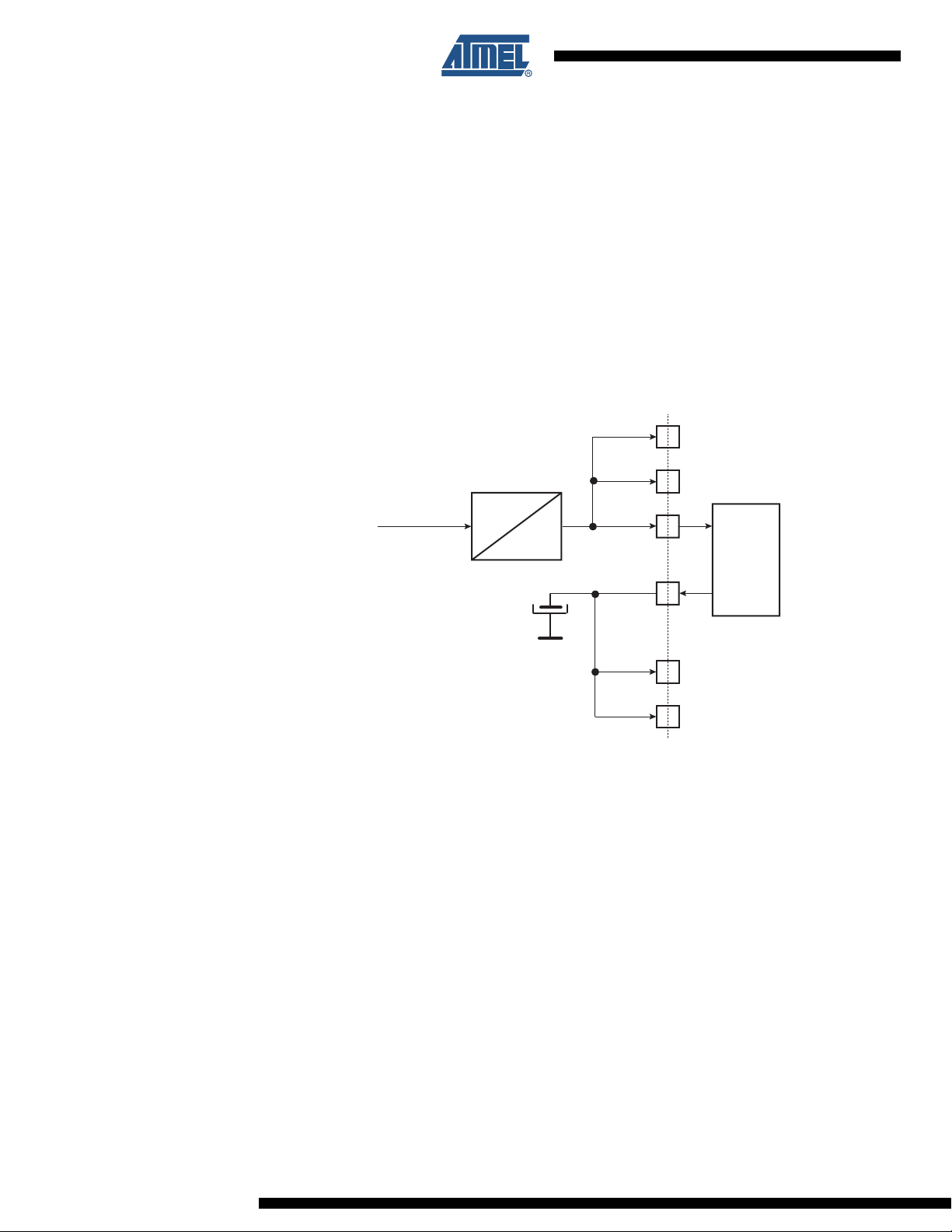
9.2 Clock Generator
The Clock Generator embeds one low-power RC Oscillator, one Main Oscillator and one PLL
with the following characteristics:
30
• RC Oscillator ranges between 22 KHz and 42 KHz
AT91SAM7SE512/256/32 Preliminary
6222ES–ATARM–04-Jan-08
Page 31

AT91SAM7SE512/256/32 Preliminary Summary
• Main Oscillator frequency ranges between 3 and 20 MHz
• Main Oscillator can be bypassed
• PLL output ranges between 80 and 220 MHz
It provides SLCK, MAINCK and PLLCK.
Figure 9-2. Clock Generator Block Diagram
Clock Generator
9.3 Power Management Controller
The Power Management Controller uses the Clock Generator outputs to provide:
• the Processor Clock PCK
• the Master Clock MCK
• the USB Clock UDPCK
• all the peripheral clocks, independently controllable
• three programmable clock outputs
The Master Clock (MCK) is programmable from a few hundred Hz to the maximum operating frequency of the device.
XIN
XOUT
PLLRC
Embedded
RC
Oscillator
Main
Oscillator
PLL and
Divider
Status
Power
Management
Controller
Control
Slow Clock
SLCK
Main Clock
MAINCK
PLL Clock
PLLCK
6222ES–ATARM–04-Jan-08
The Processor Clock (PCK) switches off when entering processor idle mode, thus allowing
reduced power consumption while waiting for an interrupt.
31
Page 32

Figure 9-3. Power Management Controller Block Diagram
9.4 Advanced Interrupt Controller
• Controls the interrupt lines (nIRQ and nFIQ) of an ARM Processor
• Individually maskable and vectored interrupt sources
– Source 0 is reserved for the Fast Interrupt Input (FIQ)
– Source 1 is reserved for system peripherals (RTT, PIT, EFC, PMC, DBGU, etc.)
– Other sources control the peripheral interrupts or external interrupts
– Programmable edge-triggered or level-sensitive internal sources
– Programmable positive/negative edge-triggered or high/low level-sensitive external
sources
• 8-level Priority Controller
– Drives the normal interrupt nIRQ of the processor
– Handles priority of the interrupt sources
– Higher priority interrupts can be served during service of lower priority interrupt
• Vectoring
– Optimizes interrupt service routine branch and execution
– One 32-bit vector register per interrupt source
– Interrupt vector register reads the corresponding current interrupt vector
•Protect Mode
– Easy debugging by preventing automatic operations
•Fast Forcing
– Permits redirecting any interrupt source on the fast interrupt
• General Interrupt Mask
– Provides processor synchronization on events without triggering an interrupt
SLCK
MAINCK
PLLCK
SLCK
MAINCK
PLLCK
Master Clock Controller
Programmable Clock Controller
PLLCK
Prescaler
/1,/2,/4,...,/64
Prescaler
/1,/2,/4,...,/64
USB Clock Controller
ON/OFF
Divider
/1,/2,/4
Processor
Clock
Controller
Idle Mode
Peripherals
Clock Controller
ON/OFF
PCK
int
MCK
periph_clk[2..14]
pck[0..2]
usb_suspend
UDPCK
32
AT91SAM7SE512/256/32 Preliminary
6222ES–ATARM–04-Jan-08
Page 33

9.5 Debug Unit
AT91SAM7SE512/256/32 Preliminary Summary
• Comprises:
– One two-pin UART
– One Interface for the Debug Communication Channel (DCC) support
– One set of Chip ID Registers
– One Interface providing ICE Access Prevention
•Two-pin UART
– USART-compatible User Interface
– Programmable Baud Rate Generator
– Parity, Framing and Overrun Error
– Automatic Echo, Local Loopback and Remote Loopback Channel Modes
• Debug Communication Channel Support
– Offers visibility of COMMRX and COMMTX signals from the ARM Processor
• Chip ID Registers
– Identification of the device revision, sizes of the embedded memories, set of
peripherals
– Chip ID is 0x272A 0A40 (VERSION 0) for AT91SAM7SE512
– Chip ID is 0x272A 0940 (VERSION 0) for AT91SAM7SE256
– Chip ID is 0x2728 0340 (VERSION 0) for AT91SAM7SE32
9.6 Periodic Interval Timer
• 20-bit programmable counter plus 12-bit interval counter
9.7 Watchdog Timer
• 12-bit key-protected Programmable Counter running on prescaled SLCK
• Provides reset or interrupt signals to the system
• Counter may be stopped while the processor is in debug state or in idle mode
9.8 Real-time Timer
• 32-bit free-running counter with alarm running on prescaled SLCK
• Programmable 16-bit prescaler for SLCK accuracy compensation
9.9 PIO Controllers
• Three PIO Controllers. PIO A and B each control 32 I/O lines and PIO C controls 24 I/O lines.
• Fully programmable through set/clear registers
• Multiplexing of two peripheral functions per I/O line
• For each I/O line (whether assigned to a peripheral or used as general-purpose I/O)
– Input change interrupt
– Half a clock period glitch filter
– Multi-drive option enables driving in open drain
– Programmable pull-up on each I/O line
– Pin data status register, supplies visibility of the level on the pin at any time
6222ES–ATARM–04-Jan-08
33
Page 34

• Synchronous output, provides Set and Clear of several I/O lines in a single write
9.10 Voltage Regulator Controller
The purpose of this controller is to select the Power Mode of the Voltage Regulator between
Normal Mode (bit 0 is cleared) or Standby Mode (bit 0 is set).
34
AT91SAM7SE512/256/32 Preliminary
6222ES–ATARM–04-Jan-08
Page 35

AT91SAM7SE512/256/32 Preliminary Summary
10. Peripherals
10.1 User Interface
The User Peripherals are mapped in the 256 MBytes of the address space between
0xF000 0000 and 0xFFFF EFFF. Each peripheral is allocated 16 Kbytes of address space.
A complete memory map is presented in Figure 8-1 on page 22.
10.2 Peripheral Identifiers
The AT91SAM7SE512/256/32 embeds a wide range of peripherals. Table 10-1 defines the
Peripheral Identifiers of the AT91SAM7SE512/256/32. Unique peripheral identifiers are defined
for both the Advanced Interrupt Controller and the Power Management Controller.
Table 10-1. Peripheral Identifiers
Peripheral
ID
0 AIC Advanced Interrupt Controller FIQ
1 SYSC
2 PIOA Parallel I/O Controller A
3 PIOB Parallel I/O Controller B
4 PIOC Parallel I/O Controller C
5 SPI Serial Peripheral Interface 0
6 US0 USART 0
7 US1 USART 1
8 SSC Synchronous Serial Controller
9 TWI Two-wire Interface
10 PWMC PWM Controller
11 UDP USB Device Port
12 TC0 Timer/Counter 0
13 TC1 Timer/Counter 1
14 TC2 Timer/Counter 2
15 ADC
16-28 reserved
29 AIC Advanced Interrupt Controller IRQ0
30 AIC Advanced Interrupt Controller IRQ1
Peripheral
Mnemonic
(1)
(1)
Peripheral
Name
Analog-to Digital Converter
External
Interrupt
6222ES–ATARM–04-Jan-08
Note: 1. Setting SYSC and ADC bits in the clock set/clear registers of the PMC has no effect. The Sys-
tem Controller is continuously clocked. The ADC clock is automatically started for the first
conversion. In Sleep Mode the ADC clock is automatically stopped after each conversion.
35
Page 36

10.3 Peripheral Multiplexing on PIO Lines
The AT91SAM7SE512/256/32 features three PIO controllers, PIOA, PIOB and PIOC, that multiplex the I/O lines of the peripheral set.
PIO Controller A and B control 32 lines; PIO Controller C controls 24 lines. Each line can be
assigned to one of two peripheral functions, A or B. Some of them can also be multiplexed with
the analog inputs of the ADC Controller.
Table 10-2 on page 37 defines how the I/O lines of the peripherals A and B or the analog inputs
are multiplexed on the PIO Controller A, B and C. The two columns “Function” and “Comments”
have been inserted for the user’s own comments; they may be used to track how pins are
defined in an application.
Note that some peripheral functions that are output only may be duplicated in the table.
At reset, all I/O lines are automatically configured as input with the programmable pull-up
enabled, so that the device is maintained in a static state as soon as a reset is detected.
36
AT91SAM7SE512/256/32 Preliminary
6222ES–ATARM–04-Jan-08
Page 37

AT91SAM7SE512/256/32 Preliminary Summary
10.4 PIO Controller A Multiplexing
Table 10-2. Multiplexing on PIO Controller A
PIO Controller A Application Usage
I/O Line Peripheral A Peripheral B Comments Function Comments
PA0 PWM0 A0/NBS0 High-Drive
PA1 PWM1 A1/NBS2 High-Drive
PA2 PWM2 A2 High-Drive
PA3 TWD A3 High-Drive
PA 4 T WC K A 4
PA 5 R XD 0 A 5
PA 6 T XD 0 A 6
PA 7 RT S 0 A 7
PA 8 C TS 0 A 8
PA9 DRXD A9
PA 10 D TX D A 1 0
PA11 NPCS0 A11
PA12 MISO A12
PA13 MOSI A13
PA14 SPCK A14
PA 15 T F A 1 5
PA16 TK A16/BA0
PA17 TD A17/BA1 AD0
PA18 RD NBS3/CFIOW AD1
PA 19
PA 20
PA21 RXD1 NCS6/CFCE2
PA22 TXD1 NCS5/CFCE1
PA23 SCK1 NWR1/NBS1/CFIOR
PA24 RTS1 SDA10
PA25 CTS1 SDCKE
PA26 DCD1 NCS1/SDCS
PA27 DTR1 SDWE
PA28 DSR1 CAS
RK NCS4/CFCS0 AD2
RF NCS2/CFCS1 AD3
PA 29 R I1 R A S
PA30 IRQ1 D30
PA31 NPCS1 D31
6222ES–ATARM–04-Jan-08
37
Page 38

10.5 PIO Controller B Multiplexing
Table 10-3. Multiplexing on PIO Controller B
PIO Controller B Application Usage
I/O Line Peripheral A Peripheral B Comments Function Comments
PB0 TIOA0 A0/NBS0
PB1 TIOB0 A1/NBS2
PB2 SCK0 A2
PB3 NPCS3 A3
PB4 TCLK0 A4
PB5 NPCS3 A5
PB6 PCK0 A6
PB7 PWM3 A7
PB8 ADTRG A8
PB9 NPCS1 A9
PB10 NPCS2 A10
PB11 PWM0 A11
PB12 PWM1 A12
PB13 PWM2 A13
PB14 PWM3 A14
PB15 TIOA1 A15
PB16 TIOB1 A16/BA0
PB17 PCK1 A17/BA1
PB18 PCK2 D16
PB19 FIQ D17
PB20 IRQ0 D18
PB21 PCK1 D19
PB22 NPCS3 D20
PB23 PWM0 D21
PB24 PWM1 D22
PB25 PWM2 D23
PB26 TIOA2 D24
PB27 TIOB2 D25
PB28 TCLK1 D26
PB29 TCLK2 D27
PB30 NPCS2 D28
PB31 PCK2 D29
38
AT91SAM7SE512/256/32 Preliminary
6222ES–ATARM–04-Jan-08
Page 39

AT91SAM7SE512/256/32 Preliminary Summary
10.6 PIO Controller C Multiplexing
Multiplexing on PIO Controller C
PIO Controller C Application Usage
I/O Line Peripheral A Peripheral B Comments Function Comments
PC0 D0
PC1 D1
PC2 D2
PC3 D3
PC4 D4
PC5 D5
PC6 D6
PC7 D7
PC8 D8 RTS1
PC9 D9 DTR1
PC10 D10 PCK0
PC11 D11 PCK1
PC12 D12 PCK2
PC13 D13
PC14 D14 NPCS1
PC15 D15 NCS3/NANDCS
PC16 A18 NWAIT
PC17 A19 NANDOE
PC18 A20 NANDWE
PC19 A21/NANDALE
PC20 A22/REG/NANDCLE NCS7
PC21 NWR0/NWE/CFWE
PC22 NRD/CFOE
PC23 CFRNW NCS0
10.7 Serial Peripheral Interface
• Supports communication with external serial devices
– Four chip selects with external decoder allow communication with up to 15
peripherals
– Serial memories, such as DataFlash
– Serial peripherals, such as ADCs, DACs, LCD Controllers, CAN Controllers and
Sensors
– External co-processors
• Master or slave serial peripheral bus interface
®
and 3-wire EEPROMs
6222ES–ATARM–04-Jan-08
39
Page 40

10.8 Two Wire Interface
• Master, Multi-Master and Slave Mode Operation
• Compatibility with standard two-wire serial memories
• One, two or three bytes for slave address
• Sequential read/write operations
• Bit Rate: Up to 400 Kbit/s
• General Call Supported in Slave Mode
10.9 USART
• Programmable Baud Rate Generator
• 5- to 9-bit full-duplex synchronous or asynchronous serial communications
• RS485 with driver control signal
• ISO7816, T = 0 or T = 1 Protocols for interfacing with smart cards
•IrDA
• Test Modes
– 8- to 16-bit programmable data length per chip select
– Programmable phase and polarity per chip select
– Programmable transfer delays per chip select, between consecutive transfers and
between clock and data
– Programmable delay between consecutive transfers
– Selectable mode fault detection
– Maximum frequency at up to Master Clock
– 1, 1.5 or 2 stop bits in Asynchronous Mode
– 1 or 2 stop bits in Synchronous Mode
– Parity generation and error detection
– Framing error detection, overrun error detection
– MSB or LSB first
– Optional break generation and detection
– By 8 or by 16 over-sampling receiver frequency
– Hardware handshaking RTS - CTS
– Modem Signals Management DTR-DSR-DCD-RI on USART1
– Receiver time-out and transmitter timeguard
– Multi-drop Mode with address generation and detection
– NACK handling, error counter with repetition and iteration limit
®
modulation and demodulation
– Communication at up to 115.2 Kbps
– Remote Loopback, Local Loopback, Automatic Echo
10.10 Serial Synchronous Controller
• Provides serial synchronous communication links used in audio and telecom applications
• Contains an independent receiver and transmitter and a common clock divider
40
AT91SAM7SE512/256/32 Preliminary
6222ES–ATARM–04-Jan-08
Page 41

10.11 Timer Counter
AT91SAM7SE512/256/32 Preliminary Summary
• Offers a configurable frame sync and data length
• Receiver and transmitter can be programmed to start automatically or on detection of
different event on the frame sync signal
• Receiver and transmitter include a data signal, a clock signal and a frame synchronization
signal
• Three 16-bit Timer Counter Channels
– Two output compare or one input capture per channel
• Wide range of functions including:
– Frequency measurement
– Event counting
– Interval measurement
– Pulse generation
– Delay timing
– Pulse Width Modulation
– Up/down capabilities
• Each channel is user-configurable and contains:
– Three external clock inputs
– Five internal clock inputs, as defined in Table 10-4
Table 10-4. Timer Counter Clocks Assignment
10.12 PWM Controller
TC Clock input Clock
TIMER_CLOCK1 MCK/2
TIMER_CLOCK2 MCK/8
TIMER_CLOCK3 MCK/32
TIMER_CLOCK4 MCK/128
TIMER_CLOCK5 MCK/1024
– Two multi-purpose input/output signals
– Two global registers that act on all three TC channels
• Four channels, one 16-bit counter per channel
• Common clock generator, providing thirteen different clocks
– One Modulo n counter providing eleven clocks
– Two independent linear dividers working on modulo n counter outputs
• Independent channel programming
– Independent enable/disable commands
– Independent clock selection
– Independent period and duty cycle, with double buffering
– Programmable selection of the output waveform polarity
– Programmable center or left aligned output waveform
6222ES–ATARM–04-Jan-08
41
Page 42

10.13 USB Device Port
• USB V2.0 full-speed compliant,12 Mbits per second.
• Embedded USB V2.0 full-speed transceiver
• Embedded 2688-byte dual-port RAM for endpoints
• Eight endpoints
– Endpoint 0: 64bytes
– Endpoint 1 and 2: 64 bytes ping-pong
– Endpoint 3: 64 bytes
– Endpoint 4 and 5: 512 bytes ping-pong
– Endpoint 6 and 7: 64 bytes ping-pong
– Ping-pong Mode (two memory banks) for Isochronous and bulk endpoints
• Suspend/resume logic
• Integrated Pull-up on DDP
10.14 Analog-to-Digital Converter
• 8-channel ADC
• 10-bit 384 Ksamples/sec. or 8-bit 583 Ksamples/sec. Successive Approximation Register
ADC
• ±2 LSB Integral Non Linearity, ±1 LSB Differential Non Linearity
• Integrated 8-to-1 multiplexer, offering eight independent 3.3V analog inputs
• External voltage reference for better accuracy on low voltage inputs
• Individual enable and disable of each channel
• Multiple trigger sources
– Hardware or software trigger
– External trigger pin
– Timer Counter 0 to 2 outputs TIOA0 to TIOA2 trigger
• Sleep Mode and conversion sequencer
– Automatic wakeup on trigger and back to sleep mode after conversions of all
enabled channels
• Each analog input shared with digital signals
42
AT91SAM7SE512/256/32 Preliminary
6222ES–ATARM–04-Jan-08
Page 43

AT91SAM7SE512/256/32 Preliminary Summary
11. Package Drawings
Figure 11-1. 128-lead LQFP Package Drawing
6222ES–ATARM–04-Jan-08
43
Page 44

Figure 11-2. 144-ball LFBGA Package Drawing
All dimensions are in mm
44
AT91SAM7SE512/256/32 Preliminary
6222ES–ATARM–04-Jan-08
Page 45

AT91SAM7SE512/256/32 Preliminary Summary
12. Ordering Information
Table 12-1. Ordering Information
Ordering Code Package Package Type
Temperature
Operating Range
AT91SAM7SE512-AU LQFP128 Green
AT91SAM7SE256-AU LQFP128 Green
AT91SAM7SE32-AU LQFP128 Green
AT91SAM7SE512-CU LFBGA144 Green
AT91SAM7SE256-CU LFBGA144 Green
AT91SAM7SE32-CU LFBGA144 Green
Industrial
(-40°C to 85°C)
Industrial
(-40°C to 85°C)
Industrial
(-40°C to 85°C)
Industrial
(-40°C to 85°C)
Industrial
(-40°C to 85°C)
Industrial
(-40°C to 85°C)
6222ES–ATARM–04-Jan-08
45
Page 46

Revision History
Change
Request
Doc. Rev Comments
First issue
6222AS
6222BS Section 12. “Ordering Information” on page 45 ordering information code reference changed #3699
6222CS
Revised Memories with condensed mapping.
Added Package Outlines and 144-ball LFBGA pin and ordering information.
Section 6.1 ”JTAG Port Pins”, Section 6.3 ”Reset Pin”, Section 6.5 ”SDCK Pin”, removed statement: “not 5V
tolerant”
Section 7.6 ”SDRAM Controller”, Mobile SDRAM controller added to SDRAMC features
INL and DNL updated in Section 10.14 ”Analog-to-Digital Converter”
“Features” on page 2, Fully Static Operation; added, up to 55 MHz at 1.8V and 85°C worst case conditions
Section 7.1 ”ARM7TDMI Processor”, Runs at up to 55 MHz, providing 0.9 MIPS/MHz (core supplied with 1.8V)
Section 7.8 ”Peripheral DMA Controller” PDC priority list added
Section 7.5 ”Static Memory Controller”, Multiple device adaptability includes: compliant w/PSRAM in
synchronous operations.
Ref.
#2709
#3826
#4005
#3924
#3833
review
Figure 8-1 ”AT91SAM7SE Memory Mapping” Compact Flash not shown w/EBI Chip Select 5. Compact Flash is
shown with EBI Chip Select 2.
6222DS
6222ES Section 10.11 ”Timer Counter”, .....the TC has two ouput compare and one input capture per channel. 4209
Section 8.1.2.1 ”Flash Overview”, updated AT91SAM7SE32 ...”reads as 8192 32-bit words.”
Section 6. ”/O Lines Considerations”, “JTAG Port Pins”, “Test Pin”, “Reset Pin”, “ERASE Pin” descriptions
updated
4804
4512
5062
46
AT91SAM7SE512/256/32 Preliminary
6222ES–ATARM–04-Jan-08
 Loading...