

Datasheet AT91SAM7S512, AT91SAM7S256, AT91SAM7S128, AT91SAM7S64, AT91SAM7S321 Datasheet (ATMEL)
...Page 1

Features
• Incorporates the ARM7TDMI
– High-performance 32-bit RISC Architecture
– High-density 16-bit Instruction Set
– Leader in MIPS/Watt
– EmbeddedICE
• Internal High-speed Flash
– 512 Kbytes (AT91SAM7S512) Organized in Two Contiguous Banks of 1024 Pages
of 256 Bytes (Dual Plane)
– 256 kbytes(AT91SAM7S256) Organized in 1024 Pages of 256 Bytes (Single Plane)
– 128 Kbytes (AT91SAM7S128) Organized in 512 Pages of 256 Bytes (Single Plane)
– 64 Kbytes (AT91SAM7S64) Organized in 512 Pages of 128 Bytes (Single Plane)
– 32 Kbytes (AT91SAM7S321/32) Organized in 256 Pages of 128 Bytes (Single Plane)
– Single Cycle Access at Up to 30 MHz in Worst Case Conditions
– Prefetch Buffer Optimizing Thumb Instruction Execution at Maximum Speed
– Page Programming Time: 6 ms, Including Page Auto-erase, Full Erase Time: 15 ms
– 10,000 Write Cycles, 10-year Data Retention Capability, Sector Lock Capabilities,
Flash Security Bit
– Fast Flash Programming Interface for High Volume Production
• Internal High-speed SRAM, Single-cycle Access at Maximum Speed
– 64 kbytes (AT91SAM7S512/256)
– 32 kbytes (AT91SAM7S128)
– 16 kbytes (AT91SAM7S64)
– 8 kbytes (AT91SAM7S321/32)
• Memory Controller (MC)
– Embedded Flash Controller, Abort Status and Misalignment Detection
• Reset Controller (RSTC)
– Based on Power-on Reset and Low-power Factory-calibrated Brown-out Detector
– Provides External Reset Signal Shaping and Reset Source Status
• Clock Generator (CKGR)
– Low-power RC Oscillator, 3 to 20 MHz On-chip Oscillator and one PLL
• Power Management Controller (PMC)
– Software Power Optimization Capabilities, Including Slow Clock Mode (Down to
500 Hz) and Idle Mode
– Three Programmable External Clock Signals
• Advanced Interrupt Controller (AIC)
– Individually Maskable, Eight-level Priority, Vectored Interrupt Sources
– Two (AT91SAM7S512/256/128/64/321) or One (AT91SAM7S32) External Interrupt
Source(s) and One Fast Interrupt Source, Spurious Interrupt Protected
• Debug Unit (DBGU)
– 2-wire UART and Support for Debug Communication Channel interrupt,
Programmable ICE Access Prevention
• Periodic Interval Timer (PIT)
– 20-bit Programmable Counter plus 12-bit Interval Counter
• Windowed Watchdog (WDT)
– 12-bit key-protected Programmable Counter
– Provides Reset or Interrupt Signals to the System
– Counter May Be Stopped While the Processor is in Debug State or in Idle Mode
™
In-circuit Emulation, Debug Communication Channel Support
®
ARM® Thumb® Processor
AT91 ARM
Thumb-based
Microcontrollers
AT91SAM7S512
AT91SAM7S256
AT91SAM7S128
AT91SAM7S64
AT91SAM7S321
AT91SAM7S32
Preliminary
6175G–ATARM–22-Nov-06
Page 2

• Real-time Timer (RTT)
– 32-bit Free-running Counter with Alarm
– Runs Off the Internal RC Oscillator
• One Parallel Input/Output Controller (PIOA)
– Thirty-two (AT91SAM7S512/256/128/64/321) or twenty-one (AT91SAM7S32) Programmable I/O Lines Multiplexed with up
to Two Peripheral I/Os
– Input Change Interrupt Capability on Each I/O Line
– Individually Programmable Open-drain, Pull-up resistor and Synchronous Output
• Eleven (AT91SAM7S512/256/128/64/321) or Nine (AT91SAM7S32) Peripheral DMA Controller (PDC) Channels
• One USB 2.0 Full Speed (12 Mbits per Second) Device Port (Except for the AT91SAM7S32).
– On-chip Transceiver, 328-byte Configurable Integrated FIFOs
• One Synchronous Serial Controller (SSC)
– Independent Clock and Frame Sync Signals for Each Receiver and Transmitter
– I²S Analog Interface Support, Time Division Multiplex Support
– High-speed Continuous Data Stream Capabilities with 32-bit Data Transfer
• Two (AT91SAM7S512/256/128/64/321) or One (AT91SAM7S32) Universal Synchronous/Asynchronous Receiver Transmitters
(USART)
– Individual Baud Rate Generator, IrDA
– Support for ISO7816 T0/T1 Smart Card, Hardware Handshaking, RS485 Support
– Full Modem Line Support on USART1 (AT91SAM7S512/256/128/64/321)
®
Infrared Modulation/Demodulation
• One Master/Slave Serial Peripheral Interface (SPI)
– 8- to 16-bit Programmable Data Length, Four External Peripheral Chip Selects
• One Three (AT91SAM7S512/256/128/64/321)-channel or Two (AT91SAM7S32)-channel 16-bit Timer/Counter (TC)
– Three (AT91SAM7S512/256/128/64/321) or One (AT91SAM7S32) External Clock Input(s), Two Multi-purpose I/O Pins per
Channel
– Double PWM Generation, Capture/Waveform Mode, Up/Down Capability
• One Four-channel 16-bit PWM Controller (PWMC)
• One Two-wire Interface (TWI)
– Master Mode Support Only, All Two-wire Atmel EEPROMs Supported
• One 8-channel 10-bit Analog-to-Digital Converter, Four Channels Multiplexed with Digital I/Os
• SAM-BA
• IEEE
™
Boot Assistant
– Default Boot program
– Interface with SAM-BA Graphic User Interface
®
1149.1 JTAG Boundary Scan on All Digital Pins
• 5V-tolerant I/Os, including Four High-current Drive I/O lines, Up to 16 mA Each
• Power Supplies
– Embedded 1.8V Regulator, Drawing up to 100 mA for the Core and External Components
– 3.3V or 1.8V VDDIO I/O Lines Power Supply, Independent 3.3V VDDFLASH Flash Power Supply
– 1.8V VDDCORE Core Power Supply with Brown-out Detector
• Fully Static Operation: Up to 55 MHz at 1.65V and 85°C Worst Case Conditions
• Available in 64-lead LQFP Green or 64-pad QFN Green Package (AT91SAM7S512/256/128/64/321) and 48-lead LQFP Green or
48-pad QFN Green Package (AT91SAM7S32)
2
AT91SAM7S Series Preliminary
6175G–ATARM–22-Nov-06
Page 3

1. Description
AT91SAM7S Series Preliminary
Atmel’s AT91SAM7S is a series of low pincount Flash microcontrollers based on the 32-bit
ARM RISC processor. It features a high-speed Flash and an SRAM, a large set of peripherals,
including a USB 2.0 device (except for the AT91SAM7S32), and a complete set of system
functions minimizing the number of external components. The device is an ideal migration
path for 8-bit microcontroller users looking for additional performance and extended memory.
The embedded Flash memory can be programmed in-system via the JTAG-ICE interface or
via a parallel interface on a production programmer prior to mounting. Built-in lock bits and a
security bit protect the firmware from accidental overwrite and preserves its confidentiality.
The AT91SAM7S Series system controller includes a reset controller capable of managing the
power-on sequence of the microcontroller and the complete system. Correct device operation
can be monitored by a built-in brownout detector and a watchdog running off an integrated RC
oscillator.
The AT91SAM7S Series are general-purpose microcontrollers. Their integrated USB Device
port makes them ideal devices for peripheral applications requiring connectivity to a PC or cellular phone. Their aggressive price point and high level of integration pushes their scope of
use far into the cost-sensitive, high-volume consumer market.
Note: References to the AT91SAM7S512 in this document concern a future product under
development.
1.1 Configuration Summary of the AT91SAM7S512, AT91SAM7S256, AT91SAM7S128, AT91SAM7S64, AT91SAM7S321 and AT91SAM7S32
The AT91SAM7S512, AT91SAM7S256, AT91SAM7S128, AT91SAM7S64, AT91SAM7S321
and AT91SAM7S32 differ in memory size, peripheral set and package. Table 1-1 summarizes
the configuration of the six devices.
Except for the AT91SAM7S32, all other AT91SAM7S devices are package and pinout
compatible.
Table 1-1. Configuration Summary
USB
Flash
Device Flash
AT91SAM7S512 512K byte dual plane 64K byte 1 2
AT91SAM7S256 256K byte single plane 64K byte 1 2
AT91SAM7S128 128K byte single plane 32K byte 1 2
AT91SAM7S64 64K byte single plane 16K byte 1 2
AT91SAM7S321 32K byte single plane 8K byte 1 2
AT91SAM7S32 32K byte single plane 8K byte
Notes: 1. Fractional Baud Rate.
2. Full modem line support on USART1.
Organization SRAM
Device
Port USART
not
present
(1) (2)
(1) (2)
(1) (2)
(2)
(2)
11 9 2 21
External
Interrupt
Source
211332
211332
211332
211332
211332
PDC
Channels
TC
Channels
I/O
Lines Package
LQFP/
QFN 64
LQFP/
QFN 64
LQFP/
QFN 64
LQFP/
QFN 64
LQFP/
QFN 64
LQFP/
QFN 48
6175G–ATARM–22-Nov-06
3
Page 4
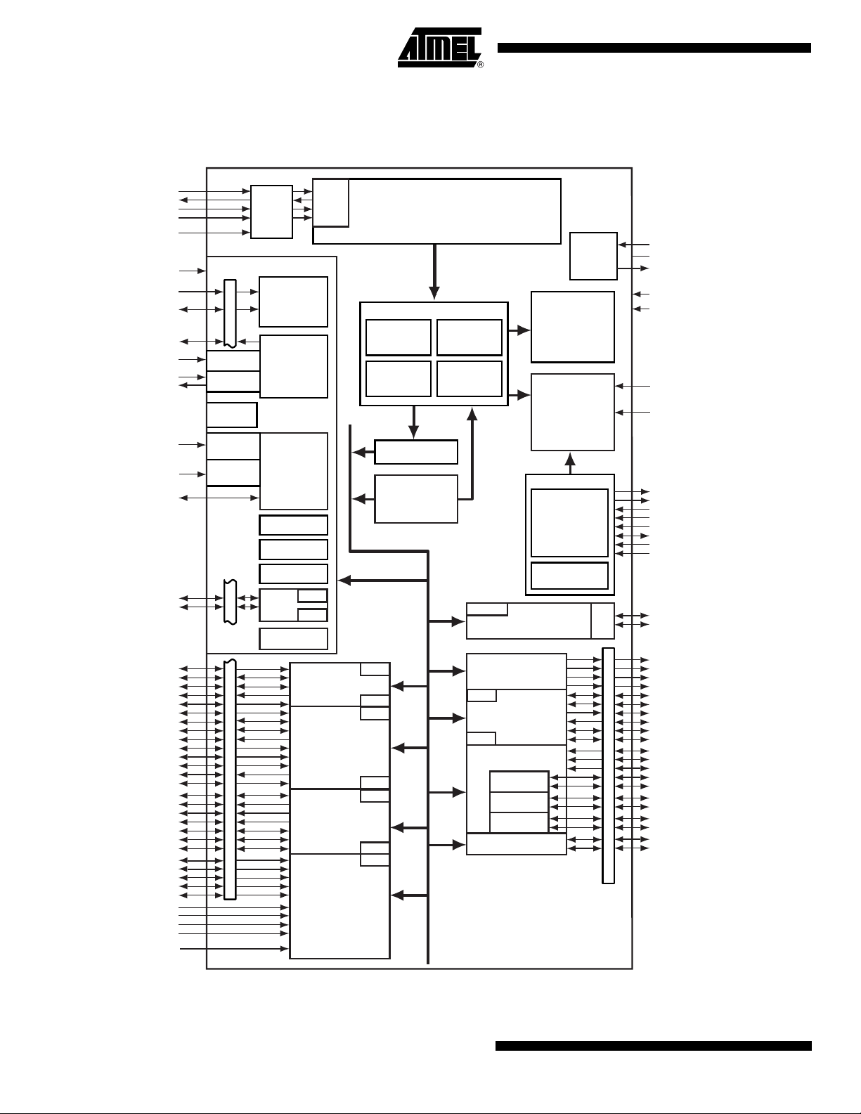
2. Block Diagram
Figure 2-1. AT91SAM7S512/256/128/64/321 Block Diagram
TDI
TDO
TMS
TCK
JTAGSEL
TST
FIQ
IRQ0-IRQ1
PCK0-PCK2
PLLRC
XIN
XOUT
VDDCORE
VDDCORE
NRST
DRXD
DTXD
RXD0
TXD0
SCK0
RTS0
CTS0
RXD1
TXD1
SCK1
RTS1
CTS1
DCD1
DSR1
DTR1
RI1
NPCS0
NPCS1
NPCS2
NPCS3
MISO
MOSI
SPCK
ADTRG
AD0
AD1
AD2
AD3
AD4
AD5
AD6
AD7
ADVREF
SCAN
System Controller
PIO
PLL
OSC
RCOSC
BOD
POR
PIO
PIO
JTAG
Controller
DBGU
AIC
PMC
Reset
PIT
WDT
RTT
PIOA
PDC
PDC
USART0
USART1
ICE
SPI
ADC
ARM7TDMI
Processor
Memory Controller
Embedded
Flash
Controller
Abort
Status
Peripheral Bridge
Peripheral Data
Controller
11 Channels
APB
PDC
PDC
PDC
PDC
PDC
PDC
PDC
Address
Decoder
Misalignment
Detection
FIFO
PDC
PDC
64/32/16/8 Kbytes
USB Device
PWMC
SSC
Timer Counter
TC0
TC1
TC2
TWI
1.8 V
Voltage
Regulator
SRAM
Flash
512/256/
128/64/32 Kbytes
ROM
Fast Flash
Programming
Interface
SAM-BA
VDDIN
GND
VDDOUT
VDDCORE
VDDIO
VDDFLASH
ERASE
PGMRDY
PGMNVALID
PGMNOE
PGMCK
PGMM0-PGMM3
PGMD0-PGMD15
PGMNCMD
PGMEN0-PGMEN2
DDM
Transceiver
PIO
DDP
PWM0
PWM1
PWM2
PWM3
TF
TK
TD
RD
RK
RF
TCLK0
TCLK1
TCLK2
TIOA0
TIOB0
TIOA1
TIOB1
TIOA2
TIOB2
TWD
TWCK
4
AT91SAM7S Series Preliminary
6175G–ATARM–22-Nov-06
Page 5
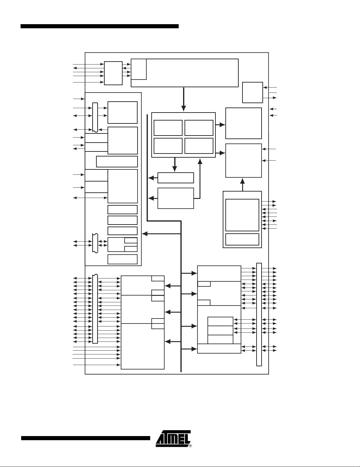
Figure 2-2. AT91SAM7S32 Block Diagram
TDI
TDO
TMS
TCK
JTAGSEL
TST
FIQ
IRQ0
PCK0-PCK2
PLLRC
XIN
XOUT
System Controller
PIO
PLL
OSC
JTAG
SCAN
RCOSC
ICE
AIC
PMC
ARM7TDMI
Processor
Memory Controller
Embedded
Flash
Controller
Abort
Status
AT91SAM7S Series Preliminary
VDDIN
GND
VDDOUT
VDDCORE
VDDIO
VDDFLASH
ERASE
Address
Decoder
Misalignment
Detection
1.8 V
Voltage
Regulator
SRAM
8 Kbytes
Flash
32 Kbytes
VDDCORE
VDDCORE
NRST
DRXD
DTXD
RXD0
TXD0
SCK0
RTS0
CTS0
NPCS0
NPCS1
NPCS2
NPCS3
MISO
MOSI
SPCK
ADTRG
AD0
AD1
AD2
AD3
AD4
AD5
AD6
AD7
ADVREF
BOD
POR
PIO
PIO
Reset
Controller
DBGU
PIT
WDT
RTT
PIOA
PDC
PDC
USART0
SPI
ADC
Peripheral Bridge
Peripheral DMA
Controller
9 Channels
APB
PDC
PDC
PDC
PDC
PDC
PDC
PDC
PWMC
SSC
Timer Counter
TC0
TC1
TC2
TWI
ROM
Fast Flash
Programming
Interface
SAM-BA
PIO
PGMRDY
PGMNVALID
PGMNOE
PGMCK
PGMM0-PGMM3
PGMD0-PGMD7
PGMNCMD
PGMEN0-PGMEN2
PWM0
PWM1
PWM2
PWM3
TF
TK
TD
RD
RK
RF
TCLK0
TIOA0
TIOB0
TIOA1
TIOB1
TWD
TWCK
6175G–ATARM–22-Nov-06
5
Page 6

3. Signal Description
Table 3-1. Signal Description List
Active
Signal Name Function Type
Power
VDDIN Voltage and ADC Regulator Power Supply Input Power 3.0 to 3.6V
VDDOUT Voltage Regulator Output Power 1.85V nominal
VDDFLASH Flash Power Supply Power 3.0V to 3.6V
VDDIO I/O Lines Power Supply Power 3.0V to 3.6V or 1.65V to 1.95V
VDDCORE Core Power Supply Power 1.65V to 1.95V
VDDPLL PLL Power 1.65V to 1.95V
GND Ground Ground
Clocks, Oscillators and PLLs
XIN Main Oscillator Input Input
XOUT Main Oscillator Output Output
PLLRC PLL Filter Input
PCK0 - PCK2 Programmable Clock Output Output
ICE and JTAG
TCK Test Clock Input No pull-up resistor
TDI Test Data In Input No pull-up resistor
TDO Test Data Out Output
TMS Test Mode Select Input No pull-up resistor
JTAGSEL JTAG Selection Input Pull-down resistor
Flash Memory
ERASE
NRST Microcontroller Reset I/O Low Open-drain with pull-Up resistor
TST Test Mode Select Input High Pull-down resistor
DRXD Debug Receive Data Input
DTXD Debug Transmit Data Output
IRQ0 - IRQ1 External Interrupt Inputs Input IRQ1 not present on AT91SAM7S32
FIQ Fast Interrupt Input Input
PA0 - PA31 Parallel IO Controller A I/O
Flash and NVM Configuration Bits Erase
Command
Reset/Test
Debug Unit
Input High Pull-down resistor
AIC
PIO
Level Comments
Pulled-up input at reset
PA0 - PA20 only on AT91SAM7S32
6
AT91SAM7S Series Preliminary
6175G–ATARM–22-Nov-06
Page 7

AT91SAM7S Series Preliminary
Table 3-1. Signal Description List (Continued)
Active
Signal Name Function Type
USB Device Port
DDM USB Device Port Data - Analog not present on AT91SAM7S32
DDP USB Device Port Data + Analog not present on AT91SAM7S32
USART
SCK0 - SCK1 Serial Clock I/O SCK1 not present on AT91SAM7S32
TXD0 - TXD1 Transmit Data I/O TXD1 not present on AT91SAM7S32
RXD0 - RXD1 Receive Data Input RXD1 not present on AT91SAM7S32
RTS0 - RTS1 Request To Send Output RTS1 not present on AT91SAM7S32
CTS0 - CTS1 Clear To Send Input CTS1 not present on AT91SAM7S32
DCD1 Data Carrier Detect Input not present on AT91SAM7S32
DTR1 Data Terminal Ready Output not present on AT91SAM7S32
DSR1 Data Set Ready Input not present on AT91SAM7S32
RI1 Ring Indicator Input not present on AT91SAM7S32
Synchronous Serial Controller
TD Transmit Data Output
RD Receive Data Input
TK Transmit Clock I/O
RK Receive Clock I/O
TF Transmit Frame Sync I/O
RF Receive Frame Sync I/O
Timer/Counter
TCLK0 - TCLK2 External Clock Inputs Input
TIOA0 - TIOA2 I/O Line A I/O TIOA2 not present on AT91SAM7S32
TIOB0 - TIOB2 I/O Line B I/O TIOB2 not present on AT91SAM7S32
PWM Controller
PWM0 - PWM3 PWM Channels Output
SPI
MISO Master In Slave Out I/O
MOSI Master Out Slave In I/O
SPCK SPI Serial Clock I/O
NPCS0 SPI Peripheral Chip Select 0 I/O Low
NPCS1-NPCS3 SPI Peripheral Chip Select 1 to 3 Output Low
Level Comments
TCLK1 and TCLK2 not present on
AT91SAM7S32
6175G–ATARM–22-Nov-06
7
Page 8

Table 3-1. Signal Description List (Continued)
Active
Signal Name Function Type
Two-Wire Interface
TWD Two-wire Serial Data I/O
TWCK Two-wire Serial Clock I/O
Analog-to-Digital Converter
AD0-AD3 Analog Inputs Analog Digital pulled-up inputs at reset
AD4-AD7 Analog Inputs Analog Analog Inputs
ADTRG ADC Trigger Input
ADVREF ADC Reference Analog
Fast Flash Programming Interface
PGMEN0-PGMEN2 Programming Enabling Input
PGMM0-PGMM3 Programming Mode Input
PGMD0-PGMD15 Programming Data I/O
PGMRDY Programming Ready Output High
PGMNVALID Data Direction Output Low
PGMNOE Programming Read Input Low
PGMCK Programming Clock Input
PGMNCMD Programming Command Input Low
Level Comments
PGMD0-PGMD7 only on
AT 91 S AM 7 S 32
8
AT91SAM7S Series Preliminary
6175G–ATARM–22-Nov-06
Page 9
AT91SAM7S Series Preliminary
4. Package and Pinout
The AT91SAM7S512/256/128/64/321 are available in a 64-lead LQFP or 64-pad QFN
package.
The AT91SAM7S32 is available in a 48-lead LQFP or 48-pad QFN package.
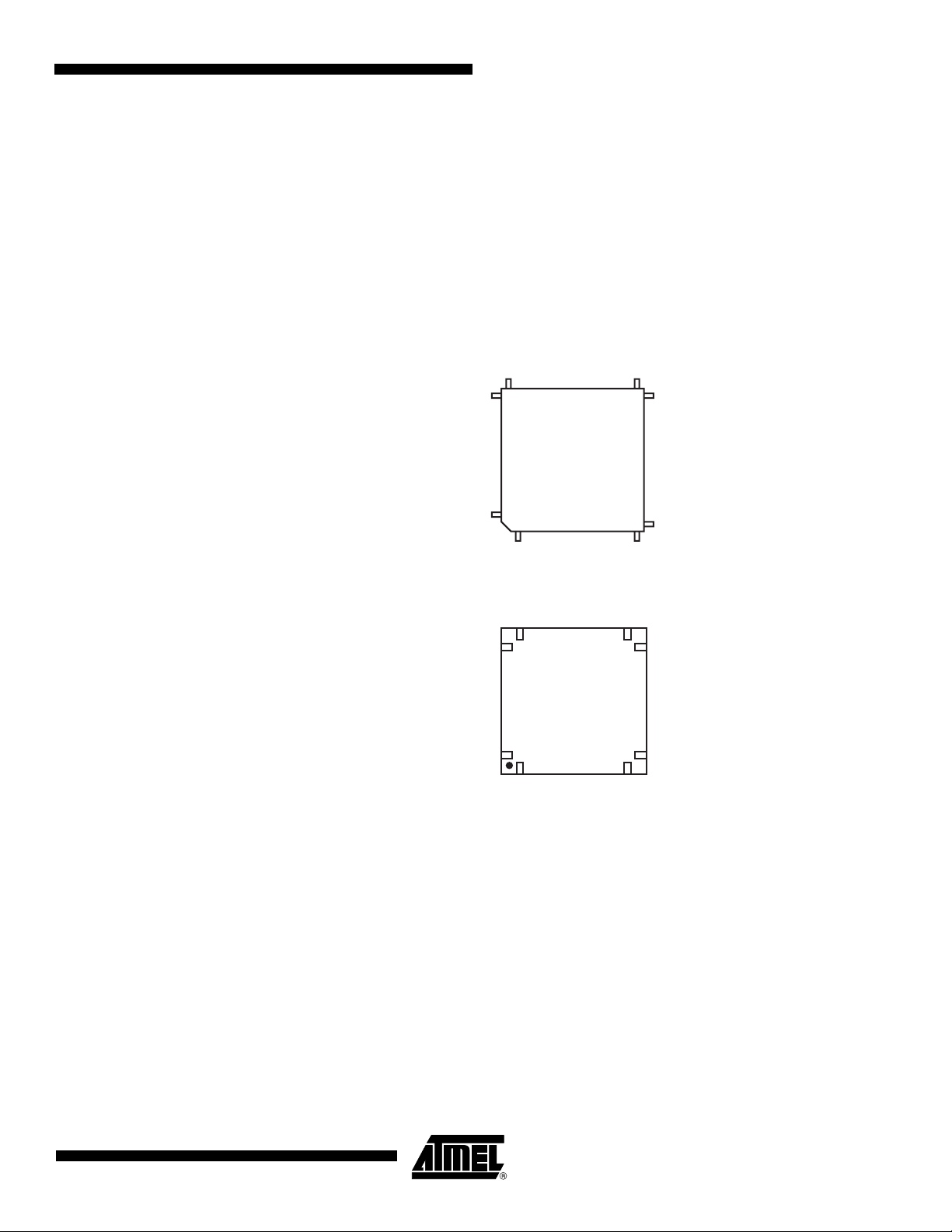
4.1 64-lead LQFP and 64-pad QFN Package Outlines
Figure 4-1 and Figure 4-2 show the orientation of the 64-lead LQFP and the 64-pad QFN
package. A detailed mechanical description is given in the section Mechanical Characteristics
of the full datasheet.
Figure 4-1. 64-lead LQFP Package (Top View)
49
3348
32
64
116
Figure 4-2. 64-pad QFN Package (Top View)
49
64
17
3348
32
17
161
6175G–ATARM–22-Nov-06
9
Page 10

4.2 64-lead LQFP and 64-pad QFN Pinout
Table 4-1. AT91SAM7S512/256/128/64/321 Pinout
1 ADVREF 17 GND 33 TDI 49 TDO
2 GND 18 VDDIO 34 PA6/PGMNOE 50 JTAGSEL
3 AD4 19 PA16/PGMD4 35 PA5/PGMRDY 51 TMS
4 AD5 20 PA15/PGMD3 36 PA4/PGMNCMD 52 PA31
5 AD6 21 PA14/PGMD2 37 PA27/PGMD15 53 TCK
6 AD7 22 PA13/PGMD1 38 PA28 54 VDDCORE
7 VDDIN 23 PA24/PGMD12 39 NRST 55 ERASE
8 VDDOUT 24 VDDCORE 40 TST 56 DDM
9 PA17/PGMD5/AD0 25 PA25/PGMD13 41 PA29 57 DDP
10 PA18/PGMD6/AD1 26 PA26/PGMD14 42 PA30 58 VDDIO
11 PA21/PGMD9 27 PA12/PGMD0 43 PA3 59 VDDFLASH
12 VDDCORE 28 PA11/PGMM3 44 PA2/PGMEN2 60 GND
13 PA19/PGMD7/AD2 29 PA10/PGMM2 45 VDDIO 61 XOUT
14 PA22/PGMD10 30 PA9/PGMM1 46 GND 62 XIN/PGMCK
15 PA23/PGMD11 31 PA8/PGMM0 47 PA1/PGMEN1 63 PLLRC
16 PA20/PGMD8/AD3 32 PA7/PGMNVALID 48 PA0/PGMEN0 64 VDDPLL
Note: 1. The bottom pad of the QFN package must be connected to ground.
(1)
10
AT91SAM7S Series Preliminary
6175G–ATARM–22-Nov-06
Page 11
AT91SAM7S Series Preliminary
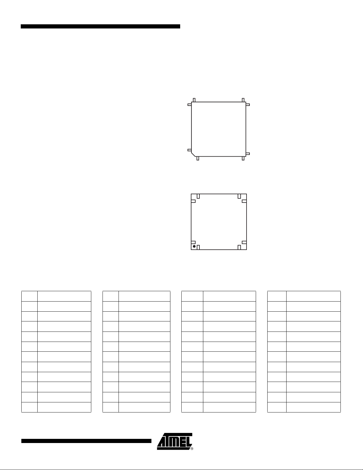
4.3 48-lead LQFP and 48-pad QFN Package Outlines
Figure 4-3 and Figure 4-4 show the orientation of the 48-lead LQFP and the 48-pad QFN
package. A detailed mechanical description is given in the section Mechanical Characteristics
of the full datasheet.
Figure 4-3. 48-lead LQFP Package (Top View)
37
2536
24
48
112
13
Figure 4-4. 48-pad QFN Package (Top View)
2536
37
48
24
13
121
4.4 48-lead LQFP and 48-pad QFN Pinout
Table 4-2. AT91SAM7S32 Pinout
1 ADVREF 13 VDDIO 25 TDI 37 TDO
2 GND 14 PA16/PGMD4 26 PA6/PGMNOE 38 JTAGSEL
3 AD4 15 PA15/PGMD3 27 PA5/PGMRDY 39 TMS
4 AD5 16 PA14/PGMD2 28 PA4/PGMNCMD 40 TCK
(1)
5 AD6 17 PA13/PGMD1 29 NRST 41 VDDCORE
6 AD7 18 VDDCORE 30 TST 42 ERASE
7 VDDIN 19 PA12/PGMD0 31 PA3 43 VDDFLASH
8 VDDOUT 20 PA11/PGMM3 32 PA2/PGMEN2 44 GND
9 PA17/PGMD5/AD0 21 PA10/PGMM2 33 VDDIO 45 XOUT
10 PA18/PGMD6/AD1 22 PA9/PGMM1 34 GND 46 XIN/PGMCK
11 PA19/PGMD7/AD2 23 PA8/PGMM0 35 PA1/PGMEN1 47 PLLRC
12 PA20/AD3 24 PA7/PGMNVALID 36 PA0/PGMEN0 48 VDDPLL
Note: 1. The bottom pad of the QFN package must be connected to ground.
6175G–ATARM–22-Nov-06
11
Page 12

5. Power Considerations
5.1 Power Supplies
The AT91SAM7S Series has six types of power supply pins and integrates a voltage regulator,
allowing the device to be supplied with only one voltage. The six power supply pin types are:
• VDDIN pin. It powers the voltage regulator and the ADC; voltage ranges from 3.0V to 3.6V,
3.3V nominal.
• VDDOUT pin. It is the output of the 1.8V voltage regulator.
• VDDIO pin. It powers the I/O lines and the USB transceivers; dual voltage range is
supported. Ranges from 3.0V to 3.6V, 3.3V nominal or from 1.65V to 1.95V, 1.8V nominal.
Note that supplying less than 3.0V to VDDIO prevents any use of the USB transceivers.
• VDDFLASH pin. It powers a part of the Flash and is required for the Flash to operate
correctly; voltage ranges from 3.0V to 3.6V, 3.3V nominal.
• VDDCORE pins. They power the logic of the device; voltage ranges from 1.65V to 1.95V,
1.8V typical. It can be connected to the VDDOUT pin with decoupling capacitor.
VDDCORE is required for the device, including its embedded Flash, to operate correctly.
During startup, core supply voltage (VDDCORE) slope must be superior or equal to
6V/ms.
• VDDPLL pin. It powers the oscillator and the PLL. It can be connected directly to the
VDDOUT pin.
No separate ground pins are provided for the different power supplies. Only GND pins are provided and should be connected as shortly as possible to the system ground plane.
In order to decrease current consumption, if the voltage regulator and the ADC are not used,
VDDIN, ADVREF, AD4, AD5, AD6 and AD7 should be connected to GND. In this case
VDDOUT should be left unconnected.
5.2 Power Consumption
The AT91SAM7S Series has a static current of less than 60 µA on VDDCORE at 25°C, including the RC oscillator, the voltage regulator and the power-on reset. When the brown-out
detector is activated, 20 µA static current is added.
The dynamic power consumption on VDDCORE is less than 50 mA at full speed when running
out of the Flash. Under the same conditions, the power consumption on VDDFLASH does not
exceed 10 mA.
5.3 Voltage Regulator
The AT91SAM7S Series embeds a voltage regulator that is managed by the System
Controller.
In Normal Mode, the voltage regulator consumes less than 100 µA static current and draws
100 mA of output current.
The voltage regulator also has a Low-power Mode. In this mode, it consumes less than 25 µA
static current and draws 1 mA of output current.
Adequate output supply decoupling is mandatory for VDDOUT to reduce ripple and avoid
oscillations. The best way to achieve this is to use two capacitors in parallel: one external 470
pF (or 1 nF) NPO capacitor must be connected between VDDOUT and GND as close to the
12
AT91SAM7S Series Preliminary
6175G–ATARM–22-Nov-06
Page 13
chip as possible. One external 2.2 µF (or 3.3 µF) X7R capacitor must be connected between
VDDOUT and GND.
Adequate input supply decoupling is mandatory for VDDIN in order to improve startup stability
and reduce source voltage drop. The input decoupling capacitor should be placed close to the
chip. For example, two capacitors can be used in parallel: 100 nF NPO and 4.7 µF X7R.
5.4 Typical Powering Schematics
The AT91SAM7S Series supports a 3.3V single supply mode. The internal regulator is connected to the 3.3V source and its output feeds VDDCORE and the VDDPLL. Figure 5-1 shows
the power schematics to be used for USB bus-powered systems.
Figure 5-1. 3.3V System Single Power Supply Schematic
AT91SAM7S Series Preliminary
VDDFLASH
Power Source
ranges
from 4.5V (USB)
to 18V
DC/DC Converter
3.3V
VDDIO
VDDIN
Voltage
Regulator
VDDOUT
VDDCORE
VDDPLL
6175G–ATARM–22-Nov-06
13
Page 14

6. I/O Lines Considerations
6.1 JTAG Port Pins
TMS, TDI and TCK are schmitt trigger inputs. TMS and TCK are 5-V tolerant, TDI is not. TMS,
TDI and TCK do not integrate a pull-up resistor.
TDO is an output, driven at up to VDDIO, and has no pull-up resistor.
The JTAGSEL pin is used to select the JTAG boundary scan when asserted at a high level.
The JTAGSEL pin integrates a permanent pull-down resistor of about 15 kΩ to GND, so that it
can be left unconnected for normal operations.
6.2 Test Pin
The TST pin is used for manufacturing test, fast programming mode or SAM-BA Boot Recovery of the AT91SAM7S Series when asserted high. The TST pin integrates a permanent pulldown resistor of about 15 kΩ to GND, so that it can be left unconnected for normal operations.
To enter fast programming mode, the TST pin and the PA0 and PA1 pins should be tied high
and PA2 tied to low.
To enter SAM-BA Boot Recovery, the TST pin and the PA0, PA1 and PA2 pins should be tied
high.
Driving the TST pin at a high level while PA0 or PA1 is driven at 0 leads to unpredictable
results.
6.3 Reset Pin
The NRST pin is bidirectional with an open drain output buffer. It is handled by the on-chip
reset controller and can be driven low to provide a reset signal to the external components or
asserted low externally to reset the microcontroller. There is no constraint on the length of the
reset pulse, and the reset controller can guarantee a minimum pulse length. This allows connection of a simple push-button on the pin NRST as system user reset, and the use of the
signal NRST to reset all the components of the system.
The NRST pin integrates a permanent pull-up resistor to VDDIO.
6.4 ERASE Pin
The ERASE pin is used to re-initialize the Flash content and some of its NVM bits. It integrates
a permanent pull-down resistor of about 15 kΩ to GND, so that it can be left unconnected for
normal operations.
6.5 PIO Controller A Lines
All the I/O lines PA0 to PA31 (PA0 to PA20 on AT91SAM7S32) are 5V-tolerant and all integrate a programmable pull-up resistor. Programming of this pull-up resistor is performed
independently for each I/O line through the PIO controllers.
5V-tolerant means that the I/O lines can drive voltage level according to VDDIO, but can be
driven with a voltage of up to 5.5V. However, driving an I/O line with a voltage over VDDIO
while the programmable pull-up resistor is enabled will create a current path through the pullup resistor from the I/O line to VDDIO. Care should be taken, in particular at reset, as all the
I/O lines default to input with pull-up resistor enabled at reset.
14
AT91SAM7S Series Preliminary
6175G–ATARM–22-Nov-06
Page 15

6.6 I/O Line Drive Levels
The PIO lines PA0 to PA3 are high-drive current capable. Each of these I/O lines can drive up
to 16 mA permanently.
The remaining I/O lines can draw only 8 mA.
However, the total current drawn by all the I/O lines cannot exceed 150 mA (100mA for
AT91SAM7S32).
AT91SAM7S Series Preliminary
6175G–ATARM–22-Nov-06
15
Page 16

7. Processor and Architecture
7.1 ARM7TDMI Processor
• RISC processor based on ARMv4T Von Neumann architecture
– Runs at up to 55 MHz, providing 0.9 MIPS/MHz
• Two instruction sets
–ARM
–Thumb
• Three-stage pipeline architecture
– Instruction Fetch (F)
– Instruction
– Execute (E)
7.2 Debug and Test Features
• Integrated EmbeddedICE™ (embedded in-circuit emulator)
– Two watchpoint units
– Test access port accessible through a JTAG protocol
– Debug communication channel
• Debug Unit
–Two-pin UART
– Debug communication channel interrupt handling
– Chip ID Register
• IEEE1149.1 JTAG Boundary-scan on all digital pins
®
high-performance 32-bit instruction set
®
high code density 16-bit instruction set
Decode (D)
7.3 Memory Controller
• Bus Arbiter
• Address decoder provides selection signals for
• Abort Status Registers
• Misalignment Detector
• Remap Command
• Embedded Flash Controller
– Handles requests from the ARM7TDMI and the Peripheral DMA Controller
– Three internal 1 Mbyte memory areas
– One 256 Mbyte embedded peripheral area
– Source, Type and all parameters of the access leading to an abort are saved
– Facilitates debug by detection of bad pointers
– Alignment checking of all data accesses
– Abort generation in case of misalignment
– Remaps the SRAM in place of the embedded non-volatile memory
– Allows handling of dynamic exception vectors
– Embedded Flash interface, up to three programmable wait states
16
AT91SAM7S Series Preliminary
6175G–ATARM–22-Nov-06
Page 17

– Prefetch buffer, buffering and anticipating the 16-bit requests, reducing the
required wait states
– Key-protected program, erase and lock/unlock sequencer
– Single command for erasing, programming and locking operations
– Interrupt generation in case of forbidden operation
7.4 Peripheral DMA Controller
• Handles data transfer between peripherals and memories
• Eleven channels: AT91SAM7S512/256/128/64/321
• Nine channels: AT91SAM7S32
– Two for each USART
– Two for the Debug Unit
– Two for the Serial Synchronous Controller
– Two for the Serial Peripheral Interface
– One for the Analog-to-digital Converter
• Low bus arbitration overhead
– One Master Clock cycle needed for a transfer from memory to peripheral
– Two Master Clock cycles needed for a transfer from peripheral to memory
• Next Pointer management for reducing interrupt latency requirements
AT91SAM7S Series Preliminary
6175G–ATARM–22-Nov-06
17
Page 18

8. Memories
8.1 AT91SAM7S512
8.2 AT91SAM7S256
• 512 Kbytes of Flash Memory, dual plane
– 2 contiguous banks of 1024 pages of 256 bytes
– Fast access time, 30 MHz single-cycle access in Worst Case conditions
– Page programming time: 6 ms, including page auto-erase
– Page programming without auto-erase: 3 ms
– Full chip erase time: 15 ms
– 10,000 write cycles, 10-year data retention capability
– 32 lock bits, protecting 32 sectors of 64 pages
– Protection Mode to secure contents of the Flash
• 64 Kbytes of Fast SRAM
– Single-cycle access at full speed
• 256 Kbytes of Flash Memory, single plane
– 1024 pages of 256 bytes
– Fast access time, 30 MHz single-cycle access in Worst Case conditions
– Page programming time: 6 ms, including page auto-erase
– Page programming without auto-erase: 3 ms
– Full chip erase time: 15 ms
– 10,000 write cycles, 10-year data retention capability
– 16 lock bits, protecting 16 sectors of 64 pages
– Protection Mode to secure contents of the Flash
• 64 Kbytes of Fast SRAM
– Single-cycle access at full speed
8.3 AT91SAM7S128
18
AT91SAM7S Series Preliminary
• 128 Kbytes of Flash Memory, single plane
– 512 pages of 256 bytes
– Fast access time, 30 MHz single-cycle access in Worst Case conditions
– Page programming time: 6 ms, including page auto-erase
– Page programming without auto-erase: 3 ms
– Full chip erase time: 15 ms
– 10,000 write cycles, 10-year data retention capability
– 8 lock bits, protecting 8 sectors of 64 pages
– Protection Mode to secure contents of the Flash
• 32 Kbytes of Fast SRAM
– Single-cycle access at full speed
6175G–ATARM–22-Nov-06
Page 19

8.4 AT91SAM7S64
• 64 Kbytes of Flash Memory, single plane
• 16 Kbytes of Fast SRAM
8.5 AT91SAM7S321/32
• 32 Kbytes of Flash Memory, single plane
• 8 Kbytes of Fast SRAM
AT91SAM7S Series Preliminary
– 512 pages of 128 bytes
– Fast access time, 30 MHz single-cycle access in Worst Case conditions
– Page programming time: 6 ms, including page auto-erase
– Page programming without auto-erase: 3 ms
– Full chip erase time: 15 ms
– 10,000 write cycles, 10-year data retention capability
– 16 lock bits, protecting 16 sectors of 32 pages
– Protection Mode to secure contents of the Flash
– Single-cycle access at full speed
– 256 pages of 128 bytes
– Fast access time, 30 MHz single-cycle access in Worst Case conditions
– Page programming time: 6 ms, including page auto-erase
– Page programming without auto-erase: 3 ms
– Full chip erase time: 15 ms
– 10,000 write cycles, 10-year data retention capability
– 8 lock bits, protecting 8 sectors of 32 pages
– Protection Mode to secure contents of the Flash
– Single-cycle access at full speed
6175G–ATARM–22-Nov-06
19
Page 20
Figure 8-1. AT91SAM7S512/256/128/64/321/32 Memory Mapping
Internal Memory Mapping Note:
0x0000 0000
Flash before Remap
SRAM after Remap
0x000F FFF
0x0000 0000
Address Memory Space
Internal Memories
256 MBytes
0x0010 0000
0x001F FFF
0x0020 0000
0x002F FFF
0x0030 0000
Internal Flash
Internal SRAM
Reserved
(1)
1 MBytes
1 MBytes
1 MBytes
253 MBytes
(1) Can be Flash or SRAM
depending on REMAP.
0x0FFF FFFF
0x1000 0000
0xEFFF FFFF
0xF000 0000
0xFFFF FFFF
Undefined
(Abort)
Internal Peripherals
14 x 256 MBytes
3,584 MBytes
256M Bytes
0x0FFF FFFF
0xF000 0000
0xFFF9 FFFF
0xFFFA 0000
0xFFFA 3FFF
0xFFFA 4000
0xFFFA FFFF
0xFFFB 0000
0xFFFB 3FFF
0xFFFB 4000
0xFFFB 7FFF
0xFFFB 8000
0xFFFB BFFF
0xFFFB C000
0xFFFB FFFF
0xFFFC 0000
0xFFFC 3FFF
0xFFFC 4000
0xFFFC 7FFF
0xFFFC 8000
0xFFFC BFFF
0xFFFC C000
0xFFFC FFFF
0xFFFD 0000
0xFFFD 3FFF
0xFFFD 4000
0xFFFD 7FFF
0xFFFD 8000
0xFFFD BFFF
0xFFFD C000
0xFFFD FFFF
0xFFFE 0000
0xFFFE 3FFF
0xFFFE 4000
0xFFFF EFFF
0xFFFF F000
0xFFFF FFFF
Peripheral Mapping
Reserved
TC0, TC1, TC2
Reserved
UDP
Reserved
TWI
Reserved
USART0
USART1
Reserved
PWMC
Reserved
SSC
ADC
Reserved
SPI
Reserved
SYSC
16 Kbytes
16 Kbytes
(Reserved on
AT91SAM7S32)
16 Kbytes
16 Kbytes
16 Kbytes
(Reserved on
AT91SAM7S32
16 Kbytes
16 Kbytes
16 Kbytes
16 Kbytes
System Controller Mapping
0xFFFF F000
AIC
0xFFFF F1FF
0xFFFF F200
DBGU
0xFFFF F3FF
0xFFFF F400
PIOA
0xFFFF F5FF
0xFFFF F600
Reserved
0xFFFF FBFF
0xFFFF FC00
0xFFFF FCFF
0xFFFF FD00
0xFFFF FD0F
0xFFFF FD20
0xFFFF FC2F
0xFFFF FD30
0xFFFF FC3F
0xFFFF FD40
0xFFFF FD4F
0xFFFF FD60
0xFFFF FC6F
0xFFFF FD70
0xFFFF FEFF
0xFFFF FF00
0xFFFF FFFF
PMC
RSTC
Reserved
RTT
PIT
WDT
Reserved
VREG
Reserved
MC
512 Bytes/
128 registers
512 Bytes/
128 registers
512 Bytes/
128 registers
256 Bytes/
64 registers
16 Bytes/
4 registers
16 Bytes/
4 registers
16 Bytes/
4 registers
16 Bytes/
4 registers
4 Bytes/
1 register
256 Bytes/
64 registers
20
AT91SAM7S Series Preliminary
6175G–ATARM–22-Nov-06
Page 21

8.6 Memory Mapping
8.6.1 Internal SRAM
After reset and until the Remap Command is performed, the SRAM is only accessible at
address 0x0020 0000. After Remap, the SRAM also becomes available at address 0x0.
8.6.2 Internal ROM
The AT91SAM7S Series embeds an Internal ROM. The ROM contains the FFPI and the
SAM-BA program.
The internal ROM is not mapped by default.
8.6.3 Internal Flash
At any time, the Flash is mapped to address 0x0010 0000. It is also accessible at address 0x0
after the reset and before the Remap Command.
AT91SAM7S Series Preliminary
• The AT91SAM7S512 embeds a high-speed 64 Kbyte SRAM bank.
• The AT91SAM7S256 embeds a high-speed 64 Kbyte SRAM bank.
• The AT91SAM7S128 embeds a high-speed 32 Kbyte SRAM bank.
• The AT91SAM7S64 embeds a high-speed 16 Kbyte SRAM bank.
• The AT91SAM7S321 embeds a high-speed 8 Kbyte SRAM bank.
• The AT91SAM7S32 embeds a high-speed 8 Kbyte SRAM bank.
• The AT91SAM7S512 features two contiguous banks (dual plane) of 256 Kbytes of Flash.
• The AT91SAM7S256 features one bank (single plane) of 256 Kbytes of Flash.
• The AT91SAM7S128 features one bank (single plane) of 128 Kbytes of Flash.
• The AT91SAM7S64 features one bank (single plane) of 64 Kbytes of Flash.
• The AT91SAM7S321/32 features one bank (single plane) of 32 Kbytes of Flash.
6175G–ATARM–22-Nov-06
Figure 8-2. Internal Memory Mapping
256 MBytes
0x0000 0000
0x000F FFFF
0x0010 0000
0x001F FFFF
0x0020 0000
0x002F FFFF
0x0030 0000
0x0FFF FFFF
Flash Before Remap
Undefined Areas
SRAM After Remap
Internal Flash
Internal SRAM
(Abort)
1 MBytes
1 MBytes
1 MBytes
253 MBytes
21
Page 22

8.7 Embedded Flash
8.7.1 Flash Overview
The Flash benefits from the integration of a power reset cell and from the brownout detector.
This prevents code corruption during power supply changes, even in the worst conditions.
When Flash is not used (read or write access), it is automatically placed into standby mode.
• The Flash of the AT91SAM7S512 is organized in two banks (dual plane) of 1024 pages of
256 bytes. The 524,288 bytes are organized in 32-bit words.
• The Flash of the AT91SAM7S256 is organized in 1024 pages (single plane) of 256 bytes.
The 262,144 bytes are organized in 32-bit words.
• The Flash of the AT91SAM7S128 is organized in 512 pages (single plane) of 256 bytes.
The 131,072 bytes are organized in 32-bit words.
• The Flash of the AT91SAM7S64 is organized in 512 pages (single plane) of 128 bytes. The
65,536 bytes are organized in 32-bit words.
• The Flash of the AT91SAM7S321/32 is organized in 256 pages (single plane) of 128 bytes.
The 32,768 bytes are organized in 32-bit words.
• The Flash of the AT91SAM7S512/256/128 contains a 256-byte write buffer, accessible
through a 32-bit interface..
• The Flash of the AT91SAM7S64/321/32 contains a 128-byte write buffer, accessible
through a 32-bit interface.
8.7.2 Embedded Flash Controller
The Embedded Flash Controller (EFC) manages accesses performed by the masters of the
system. It enables reading the Flash and writing the write buffer. It also contains a User Interface, mapped within the Memory Controller on the APB. The User Interface allows:
• programming of the access parameters of the Flash (number of wait states, timings, etc.)
• starting commands such as full erase, page erase, page program, NVM bit set, NVM bit
clear, etc.
• getting the end status of the last command
• getting error status
• programming interrupts on the end of the last commands or on errors
The Embedded Flash Controller also provides a dual 32-bit prefetch buffer that optimizes 16bit access to the Flash. This is particularly efficient when the processor is running in Thumb
mode.
Two EFCs are embedded in the SAM7S512 to control each bank of 256 KBytes. Dual plane
organization allows concurrent Read and Program. Read from one memory plane may be performed even while program or erase functions are being executed in the other memory plane.
One EFC is embedded in the SAM7S256/128/64/32/321 to control the single plane
256/128/64/32 KBytes.
22
AT91SAM7S Series Preliminary
6175G–ATARM–22-Nov-06
Page 23

8.7.3 Lock Regions
8.7.3.1 AT91SAM7S512
Two Embedded Flash Controllers each manage 16 lock bits to protect 16 regions of the flash
against inadvertent flash erasing or programming commands. The AT91SAM7S512 contains
32 lock regions and each lock region contains 64 pages of 256 bytes. Each lock region has a
size of 16 Kbytes.
If a locked-region’s erase or program command occurs, the command is aborted and the EFC
trigs an interrupt.
The 16 NVM bits (or 32 NVM bits) are software programmable through the corresponding EFC
User Interface. The command “Set Lock Bit” enables the protection. The command “Clear
Lock Bit” unlocks the lock region.
Asserting the ERASE pin clears the lock bits, thus unlocking the entire Flash.
8.7.3.2 AT91SAM7S256
The Embedded Flash Controller manages 16 lock bits to protect 16 regions of the flash
against inadvertent flash erasing or programming commands. The AT91SAM7S256 contains
16 lock regions and each lock region contains 64 pages of 256 bytes. Each lock region has a
size of 16 Kbytes.
AT91SAM7S Series Preliminary
8.7.3.3 AT91SAM7S128
8.7.3.4 AT91SAM7S64
If a locked-region’s erase or program command occurs, the command is aborted and the EFC
trigs an interrupt.
The 16 NVM bits are software programmable through the EFC User Interface. The command
“Set Lock Bit” enables the protection. The command “Clear Lock Bit” unlocks the lock region.
Asserting the ERASE pin clears the lock bits, thus unlocking the entire Flash.
The Embedded Flash Controller manages 8 lock bits to protect 8 regions of the flash against
inadvertent flash erasing or programming commands. The AT91SAM7S128 contains 8 lock
regions and each lock region contains 64 pages of 256 bytes. Each lock region has a size of
16 Kbytes.
If a locked-region’s erase or program command occurs, the command is aborted and the EFC
trigs an interrupt.
The 8 NVM bits are software programmable through the EFC User Interface. The command
“Set Lock Bit” enables the protection. The command “Clear Lock Bit” unlocks the lock region.
Asserting the ERASE pin clears the lock bits, thus unlocking the entire Flash.
The Embedded Flash Controller manages 16 lock bits to protect 16 regions of the flash
against inadvertent flash erasing or programming commands. The AT91SAM7S64 contains
16 lock regions and each lock region contains 32 pages of 128 bytes. Each lock region has a
size of 4 Kbytes.
6175G–ATARM–22-Nov-06
If a locked-region’s erase or program command occurs, the command is aborted and the EFC
trigs an interrupt.
The 16 NVM bits are software programmable through the EFC User Interface. The command
“Set Lock Bit” enables the protection. The command “Clear Lock Bit” unlocks the lock region.
23
Page 24

Asserting the ERASE pin clears the lock bits, thus unlocking the entire Flash.
8.7.3.5 AT91SAM7S321/32
The Embedded Flash Controller manages 8 lock bits to protect 8 regions of the flash against
inadvertent flash erasing or programming commands. The AT91SAM7S321/32 contains 8 lock
regions and each lock region contains 32 pages of 128 bytes. Each lock region has a size of 4
Kbytes.
If a locked-region’s erase or program command occurs, the command is aborted and the EFC
trigs an interrupt.
The 8 NVM bits are software programmable through the EFC User Interface. The command
“Set Lock Bit” enables the protection. The command “Clear Lock Bit” unlocks the lock region.
Asserting the ERASE pin clears the lock bits, thus unlocking the entire Flash.
Table 8-1 summarizes the configuration of the six devices.
Table 8-1. Flash Configuration Summary
Device Number of Lock Bits Number of Pages in the Lock Region Page Size
AT91SAM7S512 32 64 256 bytes
AT91SAM7S256 16 64 256 bytes
AT91SAM7S128 8 64 256 bytes
AT91SAM7S64 16 32 128 bytes
AT91SAM7S321/32 8 32 128 bytes
8.7.4 Security Bit Feature
The AT91SAM7S Series features a security bit, based on a specific NVM Bit. When the security is enabled, any access to the Flash, either through the ICE interface or through the Fast
Flash Programming Interface, is forbidden. This ensures the confidentiality of the code programmed in the Flash.
This security bit can only be enabled, through the Command “Set Security Bit” of the EFC
User Interface. Disabling the security bit can only be achieved by asserting the ERASE pin at
1, and after a full flash erase is performed. When the security bit is deactivated, all accesses to
the flash are permitted.
It is important to note that the assertion of the ERASE pin should always be longer than
50 ms.
As the ERASE pin integrates a permanent pull-down, it can be left unconnected during normal
operation. However, it is safer to connect it directly to GND for the final application.
8.7.5 Non-volatile Brownout Detector Control
Two general purpose NVM (GPNVM) bits are used for controlling the brownout detector
(BOD), so that even after a power loss, the brownout detector operations remain in their state.
These two GPNVM bits can be cleared or set respectively through the commands “Clear General-purpose NVM Bit” and “Set General-purpose NVM Bit” of the EFC User Interface.
• GPNVM Bit 0 is used as a brownout detector enable bit. Setting the GPNVM Bit 0 enables
the BOD, clearing it disables the BOD. Asserting ERASE clears the GPNVM Bit 0 and thus
disables the brownout detector by default.
24
AT91SAM7S Series Preliminary
6175G–ATARM–22-Nov-06
Page 25

• The GPNVM Bit 1 is used as a brownout reset enable signal for the reset controller. Setting
the GPNVM Bit 1 enables the brownout reset when a brownout is detected, Clearing the
GPNVM Bit 1 disables the brownout reset. Asserting ERASE disables the brownout reset
by default.
8.7.6 Calibration Bits
Eight NVM bits are used to calibrate the brownout detector and the voltage regulator. These
bits are factory configured and cannot be changed by the user. The ERASE pin has no effect
on the calibration bits.
8.8 Fast Flash Programming Interface
The Fast Flash Programming Interface allows programming the device through either a serial
JTAG interface or through a multiplexed fully-handshaked parallel port. It allows gang-programming with market-standard industrial programmers.
The FFPI supports read, page program, page erase, full erase, lock, unlock and protect
commands.
The Fast Flash Programming Interface is enabled and the Fast Programming Mode is entered
when the TST pin and the PA0 and PA1 pins are all tied high and PA2 is tied low.
AT91SAM7S Series Preliminary
8.9 SAM-BA Boot Assistant
The SAM-BA™ Boot Recovery restores the SAM-BA Boot in the first two sectors of the on-chip
Flash memory. The SAM-BA Boot recovery is performed when the TST pin and the PA0, PA1
and PA2 pins are all tied high.
The SAM-BA Boot Assistant is a default Boot Program that provides an easy way to program
in situ the on-chip Flash memory.
The SAM-BA Boot Assistant supports serial communication through the DBGU or through the
USB Device Port. (The AT91SAM7S32 has no USB Device Port.)
• Communication through the DBGU supports a wide range of crystals from 3 to 20 MHz via
software auto-detection.
• Communication through the USB Device Port is limited to an 18.432 MHz crystal. (
The SAM-BA Boot provides an interface with SAM-BA Graphic User Interface (GUI).
6175G–ATARM–22-Nov-06
25
Page 26

9. System Controller
The System Controller manages all vital blocks of the microcontroller: interrupts, clocks,
power, time, debug and reset.
The System Controller peripherals are all mapped to the highest 4 Kbytes of address space,
between addresses 0xFFFF F000 and 0xFFFF FFFF.
Figure 9-1 on page 27 and Figure 9-2 on page 28 show the product specific System Controller
Block Diagrams.
Figure 8-1 on page 20 shows the mapping of the of the User Interface of the System Controller
peripherals. Note that the memory controller configuration user interface is also mapped within
this address space.
26
AT91SAM7S Series Preliminary
6175G–ATARM–22-Nov-06
Page 27
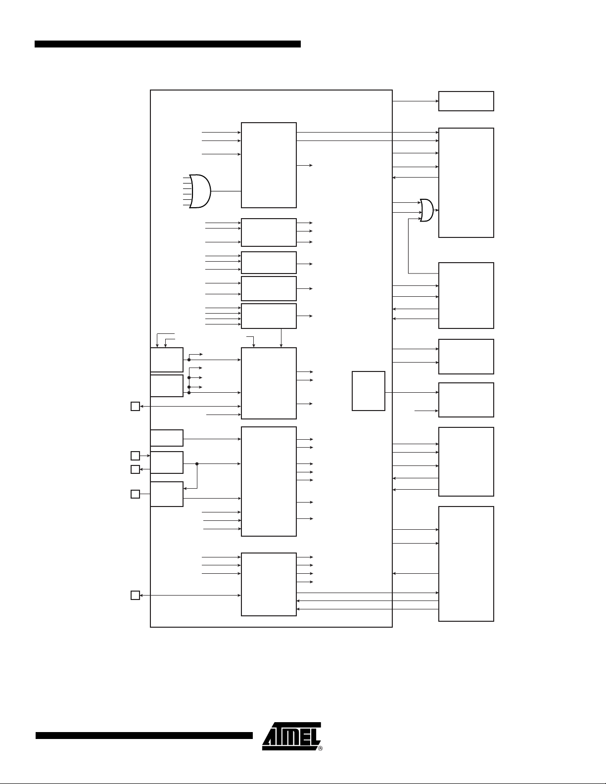
AT91SAM7S Series Preliminary
Figure 9-1. System Controller Block Diagram (AT91SAM7S512/256/128/64/321)
NRST
irq0-irq1
periph_irq[2..14]
pit_irq
rtt_irq
wdt_irq
dbgu_irq
pmc_irq
rstc_irq
periph_nreset
dbgu_rxd
debug
periph_nreset
periph_nreset
SLCK
debug
proc_nreset
cal
gpnvm[0]
en
BOD
POR
SLCK
fiq
MCK
MCK
SLCK
idle
flash_wrdis
power_on_reset
jtag_nreset
flash_poe
System Controller
Advanced
Interrupt
Controller
Debug
Unit
Periodic
Interval
Timer
Real-Time
Timer
Watchdog
Timer
gpnvm[1]
bod_rst_en
Reset
Controller
wdt_fault
WDRPROC
int
dbgu_irq
force_ntrst
dbgu_txd
pit_irq
rtt_irq
wdt_irq
periph_nreset
proc_nreset
rstc_irq
Voltage
Regulator
Mode
Controller
jtag_nreset
nirq
nfiq
proc_nreset
PCK
debug
power_on_reset
force_ntrst
security_bit
flash_poe
flash_wrdis
cal
gpnvm[0..1]
MCK
proc_nreset
standby
cal
Boundary Scan
TAP Controller
ARM7TDMI
Embedded
Flash
Memory
Controller
Voltage
Regulator
XIN
XOUT
PLLRC
PA0-PA31
RCOSC
OSC
PLL
periph_nreset
usb_suspend
periph_nreset
SLCK
MAINCK
PLLCK
periph_clk[2]
dbgu_rxd
periph_clk[2..14]
Power
Management
Controller
int
PIO
Controller
pck[0-2]
PCK
UDPCK
MCK
pmc_irq
idle
periph_irq{2]
irq0-irq1
fiq
dbgu_txd
UDPCK
periph_clk[11]
periph_nreset
periph_irq[11]
usb_suspend
periph_clk[4..14]
periph_nreset
periph_irq[4..14]
in
out
enable
USB Device
Por t
Embedded
Peripherals
6175G–ATARM–22-Nov-06
27
Page 28
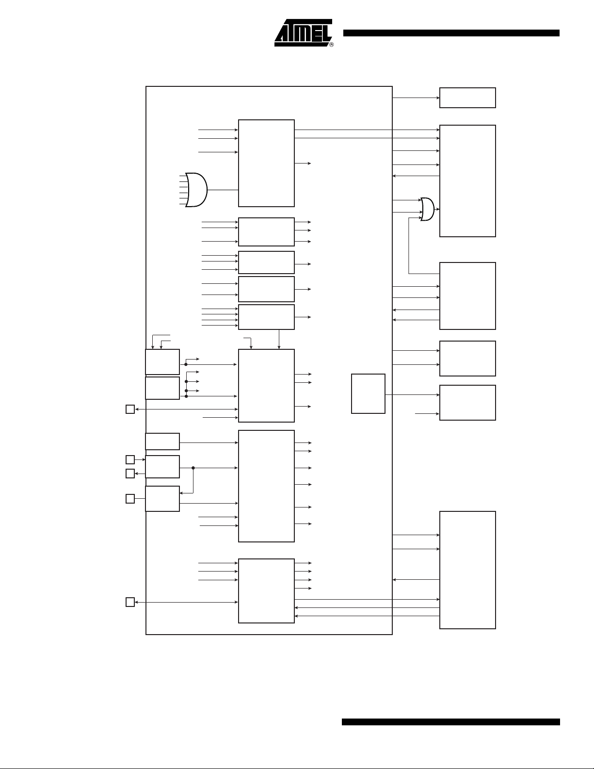
Figure 9-2. System Controller Block Diagram (AT91SAM7S32)
NRST
periph_irq[2..14]
pit_irq
rtt_irq
wdt_irq
dbgu_irq
pmc_irq
rstc_irq
periph_nreset
dbgu_rxd
periph_nreset
periph_nreset
proc_nreset
cal
gpnvm[0]
en
BOD
POR
SLCK
irq0
fiq
MCK
MCK
debug
SLCK
SLCK
debug
idle
gpnvm[1]
flash_wrdis
power_on_reset
jtag_nreset
flash_poe
System Controller
Advanced
Interrupt
Controller
Debug
Unit
Periodic
Interval
Timer
Real-Time
Timer
Watchdog
Timer
wdt_fault
WDRPROC
bod_rst_en
Reset
Controller
int
dbgu_irq
force_ntrst
dbgu_txd
pit_irq
rtt_irq
wdt_irq
periph_nreset
proc_nreset
rstc_irq
Voltage
Regulator
Mode
Controller
jtag_nreset
nirq
nfiq
proc_nreset
PCK
debug
power_on_reset
force_ntrst
security_bit
flash_poe
flash_wrdis
cal
gpnvm[0..1]
MCK
proc_nreset
standby
cal
Boundary Scan
TAP Controller
ARM7TDMI
Embedded
Flash
Memory
Controller
Voltage
Regulator
XIN
XOUT
PLLRC
PA0-PA20
RCOSC
OSC
PLL
periph_nreset
periph_nreset
periph_clk[2]
MAINCK
PLLCK
dbgu_rxd
SLCK
int
Power
Management
Controller
PIO
Controller
periph_clk[2..14]
pck[0-2]
PCK
MCK
pmc_irq
idle
periph_irq{2]
irq0
fiq
dbgu_txd
periph_clk[4..14]
periph_nreset
periph_irq[4..14]
in
out
enable
Embedded
Peripherals
28
AT91SAM7S Series Preliminary
6175G–ATARM–22-Nov-06
Page 29

9.1 Reset Controller
The Reset Controller is based on a power-on reset cell and one brownout detector. It gives the
status of the last reset, indicating whether it is a power-up reset, a software reset, a user reset,
a watchdog reset or a brownout reset. In addition, it controls the internal resets and the NRST
pin open-drain output. It allows to shape a signal on the NRST line, guaranteeing that the
length of the pulse meets any requirement.
Note that if NRST is used as a reset output signal for external devices during power-off, the
brownout detector must be activated.
9.1.1 Brownout Detector and Power-on Reset
The AT91SAM7S Series embeds a brownout detection circuit and a power-on reset cell. Both
are supplied with and monitor VDDCORE. Both signals are provided to the Flash to prevent
any code corruption during power-up or power-down sequences or if brownouts occur on the
VDDCORE power supply.
The power-on reset cell has a limited-accuracy threshold at around 1.5V. Its output remains
low during power-up until VDDCORE goes over this voltage level. This signal goes to the reset
controller and allows a full re-initialization of the device.
The brownout detector monitors the VDDCORE level during operation by comparing it to a
fixed trigger level. It secures system operations in the most difficult environments and prevents
code corruption in case of brownout on the VDDCORE.
AT91SAM7S Series Preliminary
Only VDDCORE is monitored, as a voltage drop on VDDFLASH or any other power supply of
the device cannot affect the Flash.
When the brownout detector is enabled and VDDCORE decreases to a value below the trigger
level (Vbot-, defined as Vbot - hyst/2), the brownout output is immediately activated.
When VDDCORE increases above the trigger level (Vbot+, defined as Vbot + hyst/2), the
reset is released. The brownout detector only detects a drop if the voltage on VDDCORE
stays below the threshold voltage for longer than about 1µs.
The threshold voltage has a hysteresis of about 50 mV, to ensure spike free brownout detection. The typical value of the brownout detector threshold is 1.68V with an accuracy of ± 2%
and is factory calibrated.
The brownout detector is low-power, as it consumes less than 20 µA static current. However, it
can be deactivated to save its static current. In this case, it consumes less than 1µA. The
deactivation is configured through the GPNVM bit 0 of the Flash.
6175G–ATARM–22-Nov-06
29
Page 30
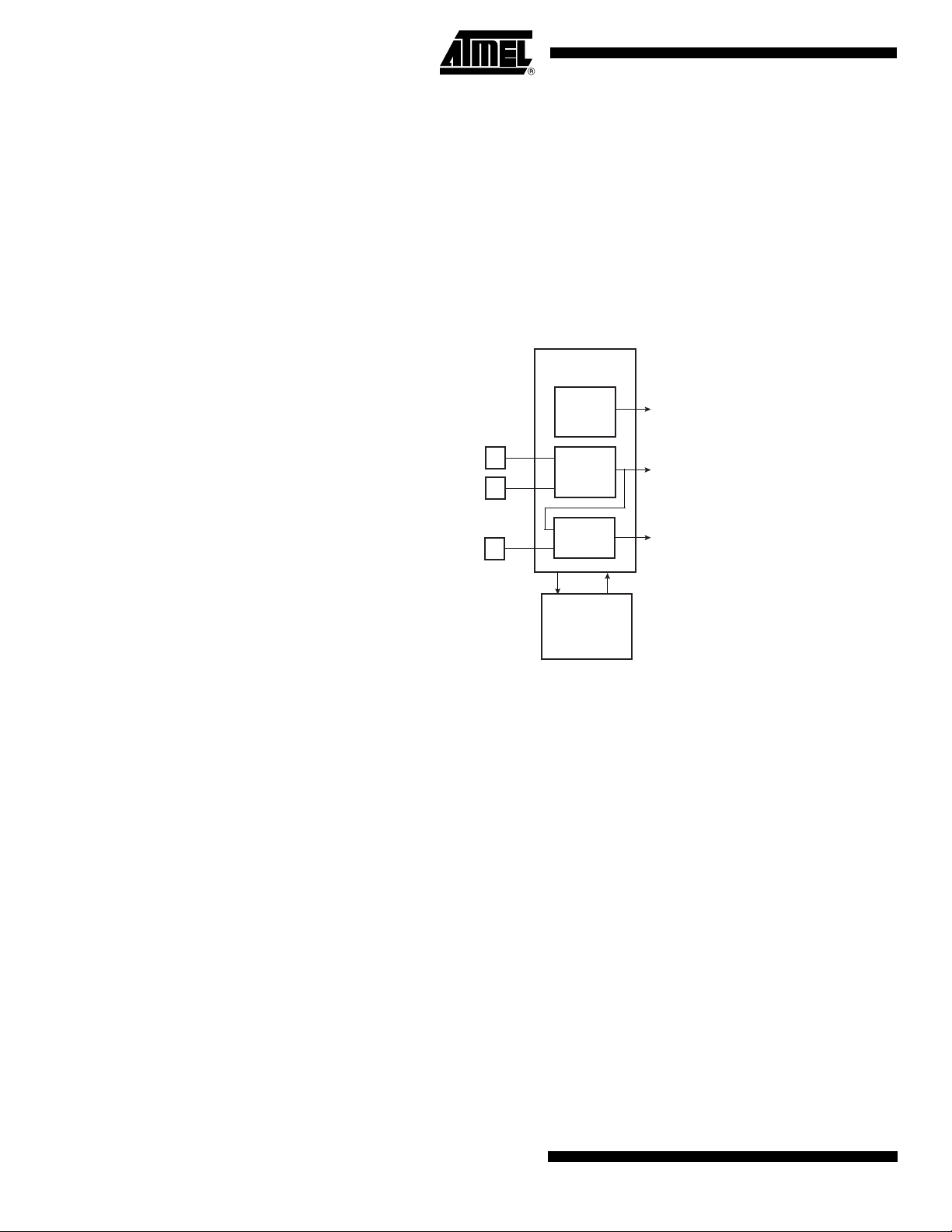
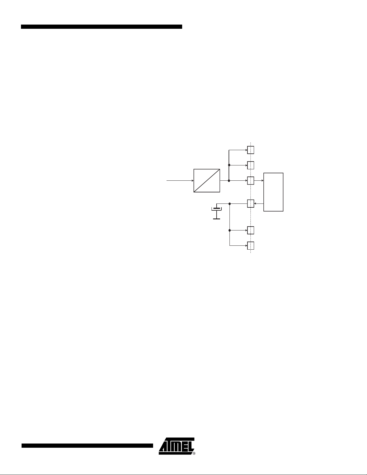
9.2 Clock Generator
The Clock Generator embeds one low-power RC Oscillator, one Main Oscillator and one PLL
with the following characteristics:
• RC Oscillator ranges between 22 kHz and 42 kHz
• Main Oscillator frequency ranges between 3 and 20 MHz
• Main Oscillator can be bypassed
• PLL output ranges between 80 and 220 MHz
It provides SLCK, MAINCK and PLLCK.
Figure 9-3. Clock Generator Block Diagram
Clock Generator
9.3 Power Management Controller
The Power Management Controller uses the Clock Generator outputs to provide:
• the Processor Clock PCK
• the Master Clock MCK
• the USB Clock UDPCK (not present on AT91SAM7S32)
• all the peripheral clocks, independently controllable
• three programmable clock outputs
The Master Clock (MCK) is programmable from a few hundred Hz to the maximum operating
frequency of the device.
XIN
XOUT
PLLRC
Embedded
RC
Oscillator
Main
Oscillator
PLL and
Divider
Status
Power
Management
Controller
Control
Slow Clock
SLCK
Main Clock
MAINCK
PLL Clock
PLLCK
30
The Processor Clock (PCK) switches off when entering processor idle mode, thus allowing
reduced power consumption while waiting for an interrupt.
AT91SAM7S Series Preliminary
6175G–ATARM–22-Nov-06
Page 31

AT91SAM7S Series Preliminary
Figure 9-4. Power Management Controller Block Diagram
9.4 Advanced Interrupt Controller
• Controls the interrupt lines (nIRQ and nFIQ) of an ARM Processor
• Individually maskable and vectored interrupt sources
– Source 0 is reserved for the Fast Interrupt Input (FIQ)
– Source 1 is reserved for system peripherals RTT, PIT, EFC, PMC, DBGU, etc.)
– Other sources control the peripheral interrupts or external interrupts
– Programmable edge-triggered or level-sensitive internal sources
– Programmable positive/negative edge-triggered or high/low level-sensitive
external sources
• 8-level Priority Controller
– Drives the normal interrupt of the processor
– Handles priority of the interrupt sources
– Higher priority interrupts can be served during service of lower priority interrupt
• Vectoring
– Optimizes interrupt service routine branch and execution
– One 32-bit vector register per interrupt source
– Interrupt vector register reads the corresponding current interrupt vector
• Protect Mode
– Easy debugging by preventing automatic operations
•Fast Forcing
– Permits redirecting any interrupt source on the fast interrupt
• General Interrupt Mask
– Provides processor synchronization on events without triggering an interrupt
SLCK
MAINCK
PLLCK
SLCK
MAINCK
PLLCK
Master Clock Controller
PLLCK
Processor
Controller
Idle Mode
Prescaler
/1,/2,/4,...,/64
Clock Controller
Programmable Clock Controller
Prescaler
/1,/2,/4,...,/64
USB Clock Controller
ON/OFF
Divider
/1,/2,/4
Clock
Peripherals
ON/OFF
PCK
int
MCK
periph_clk[2..14]
pck[0..2]
usb_suspend
UDPCK
6175G–ATARM–22-Nov-06
31
Page 32

9.5 Debug Unit
• Comprises:
– One two-pin UART
– One Interface for the Debug Communication Channel (DCC) support
– One set of Chip ID Registers
– One Interface providing ICE Access Prevention
•Two-pin UART
– Implemented features are compatible with the USART
– Programmable Baud Rate Generator
– Parity, Framing and Overrun Error
– Automatic Echo, Local Loopback and Remote Loopback Channel Modes
• Debug Communication Channel Support
– Offers visibility of COMMRX and COMMTX signals from the ARM Processor
• Chip ID Registers
– Identification of the device revision, sizes of the embedded memories, set of
peripherals
– Chip ID is 0x270B0A40 for AT91SAM7S512 (VERSION 0)
– Chip ID is 0x270B0940 for AT91SAM7S256 (VERSION 0)
– Chip ID is 0x270A0740 for AT91SAM7S128 (VERSION 0)
– Chip ID is 0x27090540 for AT91SAM7S64 (VERSION 0)
– Chip ID is 0x27080342 for AT91SAM7S321 (VERSION 0)
– Chip ID is 0x27080340 for AT91SAM7S32 (VERSION 0)
9.6 Periodic Interval Timer
• 20-bit programmable counter plus 12-bit interval counter
9.7 Watchdog Timer
• 12-bit key-protected Programmable Counter running on prescaled SCLK
• Provides reset or interrupt signals to the system
• Counter may be stopped while the processor is in debug state or in idle mode
9.8 Real-time Timer
• 32-bit free-running counter with alarm running on prescaled SCLK
• Programmable 16-bit prescaler for SLCK accuracy compensation
9.9 PIO Controller
• One PIO Controller, controlling 32 I/O lines (21 for AT91SAM7S32)
• Fully programmable through set/clear registers
• Multiplexing of two peripheral functions per I/O line
• For each I/O line (whether assigned to a peripheral or used as general-purpose I/O)
– Input change interrupt
– Half a clock period glitch filter
32
AT91SAM7S Series Preliminary
6175G–ATARM–22-Nov-06
Page 33

– Multi-drive option enables driving in open drain
– Programmable pull-up on each I/O line
– Pin data status register, supplies visibility of the level on the pin at any time
• Synchronous output, provides Set and Clear of several I/O lines in a single write
9.10 Voltage Regulator Controller
The aim of this controller is to select the Power Mode of the Voltage Regulator between Normal Mode (bit 0 is cleared) or Standby Mode (bit 0 is set).
AT91SAM7S Series Preliminary
6175G–ATARM–22-Nov-06
33
Page 34

10. Peripherals
10.1 User Interface
The User Peripherals are mapped in the 256 MBytes of address space between 0xF000 0000
and 0xFFFF EFFF. Each peripheral is allocated 16 Kbytes of address space.
A complete memory map is provided in Figure 8-1 on page 20.
10.2 Peripheral Identifiers
The AT91SAM7S Series embeds a wide range of peripherals. Table 10-1 defines the Peripheral Identifiers of the AT91SAM7S512/256/128/64/321. Table 10-2 defines the Peripheral
Identifiers of the AT91SAM7S32. A peripheral identifier is required for the control of the peripheral interrupt with the Advanced Interrupt Controller and for the control of the peripheral clock
with the Power Management Controller.
Table 10-1. Peripheral Identifiers (AT91SAM7S512/256/128/64/321)
Peripheral
ID
0 AIC Advanced Interrupt Controller FIQ
1 SYSC
2 PIOA Parallel I/O Controller A
3 Reserved
4ADC
5 SPI Serial Peripheral Interface
6 US0 USART 0
7 US1 USART 1
8 SSC Synchronous Serial Controller
9 TWI Two-wire Interface
10 PWMC PWM Controller
11 UDP USB Device Port
12 TC0 Timer/Counter 0
13 TC1 Timer/Counter 1
14 TC2 Timer/Counter 2
15 - 29 Reserved
Peripheral
Mnemonic
(1)
(1)
Peripheral
Name
System
Analog-to Digital Converter
External
Interrupt
34
30 AIC Advanced Interrupt Controller IRQ0
31 AIC Advanced Interrupt Controller IRQ1
Note: 1. Setting SYSC and ADC bits in the clock set/clear registers of the PMC has no effect. The
System Controller is continuously clocked. The ADC clock is automatically started for the
first conversion. In Sleep Mode the ADC clock is automatically stopped after each
conversion.
AT91SAM7S Series Preliminary
6175G–ATARM–22-Nov-06
Page 35

AT91SAM7S Series Preliminary
Table 10-2. Peripheral Identifiers (AT91SAM7S32)
Peripheral
ID
0 AIC Advanced Interrupt Controller FIQ
1 SYSC
2 PIOA Parallel I/O Controller A
3 Reserved
4ADC
5 SPI Serial Peripheral Interface
6 US USART
7 Reserved
8 SSC Synchronous Serial Controller
9 TWI Two-wire Interface
10 PWMC PWM Controller
11 Reserved
12 TC0 Timer/Counter 0
13 TC1 Timer/Counter 1
14 TC2 Timer/Counter 2
15 - 29 Reserved
30 AIC Advanced Interrupt Controller IRQ0
31 Reserved
Peripheral
Mnemonic
(1)
(1)
Peripheral
Name
System
Analog-to Digital Converter
External
Interrupt
Note: 1. Setting SYSC and ADC bits in the clock set/clear registers of the PMC has no effect. The
System Controller is continuously clocked. The ADC clock is automatically started for the
first conversion. In Sleep Mode the ADC clock is automatically stopped after each
conversion.
10.3 Peripheral Multiplexing on PIO Lines
The AT91SAM7S Series features one PIO controller, PIOA, that multiplexes the I/O lines of
the peripheral set.
PIO Controller A controls 32 lines (21 lines for AT91SAM7S32). Each line can be assigned to
one of two peripheral functions, A or B. Some of them can also be multiplexed with the analog
inputs of the ADC Controller.
Table 10-3, “Multiplexing on PIO Controller A (AT91SAM7S512/256/128/64/321),” on
page 36 and Table 10-4, “Multiplexing on PIO Controller A (SAM7S32),” on page 37 define
how the I/O lines of the peripherals A, B or the analog inputs are multiplexed on the PIO Controller A. The two columns “Function” and “Comments” have been inserted for the user’s own
comments; they may be used to track how pins are defined in an application.
Note that some peripheral functions that are output only may be duplicated in the table.
All pins reset in their Parallel I/O lines function are configured as input with the programmable
pull-up enabled, so that the device is maintained in a static state as soon as a reset is
detected.
6175G–ATARM–22-Nov-06
35
Page 36

10.4 PIO Controller A Multiplexing
Table 10-3. Multiplexing on PIO Controller A (AT91SAM7S512/256/128/64/321)
PIO Controller A Application Usage
I/O Line Peripheral A Peripheral B Comments Function Comments
PA0 PWM0 TIOA0 High-Drive
PA1 PWM1 TIOB0 High-Drive
PA2 PWM2 SCK0 High-Drive
PA3 TWD NPCS3 High-Drive
PA 4 T W C K T C LK 0
PA5 RXD0 NPCS3
PA 6 T X D 0 P CK 0
PA 7 R T S0 P W M3
PA8 CTS0 ADTRG
PA9 DRXD NPCS1
PA10 DTXD NPCS2
PA11 NPCS0 PWM0
PA12 MISO PWM1
PA13 MOSI PWM2
PA14 SPCK PWM3
PA15 TF TIOA1
PA16 TK TIOB1
PA17 TD PCK1 AD0
PA18 RD PCK2 AD1
PA 19 RK FIQ AD2
PA 20
PA21 RXD1 PCK1
PA22 TXD1 NPCS3
PA23 SCK1 PWM0
PA24 RTS1 PWM1
PA 25 C T S 1 P WM 2
PA26 DCD1 TIOA2
PA27 DTR1 TIOB2
PA28 DSR1 TCLK1
PA29 RI1 TCLK2
PA30 IRQ1 NPCS2
PA31 NPCS1 PCK2
RF IRQ0 AD3
36
AT91SAM7S Series Preliminary
6175G–ATARM–22-Nov-06
Page 37

AT91SAM7S Series Preliminary
Table 10-4. Multiplexing on PIO Controller A (SAM7S32)
PIO Controller A Application Usage
I/O Line Peripheral A Peripheral B Comments Function Comments
PA0 PWM0 TIOA0 High-Drive
PA1 PWM1 TIOB0 High-Drive
PA2 PWM2 SCK0 High-Drive
PA3 TWD NPCS3 High-Drive
PA 4 T W C K T C LK 0
PA5 RXD0 NPCS3
PA 6 T X D 0 P CK 0
PA 7 R T S0 P W M3
PA8 CTS0 ADTRG
PA9 DRXD NPCS1
PA10 DTXD NPCS2
PA11 NPCS0 PWM0
PA12 MISO PWM1
PA13 MOSI PWM2
PA14 SPCK PWM3
PA15 TF TIOA1
PA16 TK TIOB1
PA17 TD PCK1 AD0
PA18 RD PCK2 AD1
PA 19 RK FIQ AD2
PA 20
RF IRQ0 AD3
6175G–ATARM–22-Nov-06
37
Page 38

10.5 Serial Peripheral Interface
• Supports communication with external serial devices
– Four chip selects with external decoder allow communication with up to 15
peripherals
– Serial memories, such as DataFlash
– Serial peripherals, such as ADCs, DACs, LCD Controllers, CAN Controllers and
Sensors
– External co-processors
• Master or slave serial peripheral bus interface
– 8- to 16-bit programmable data length per chip select
– Programmable phase and polarity per chip select
– Programmable transfer delays between consecutive transfers and between clock
and data per chip select
– Programmable delay between consecutive transfers
– Selectable mode fault detection
– Maximum frequency at up to Master Clock
10.6 Two-wire Interface
• Master Mode only
• Compatibility with standard two-wire serial memories
• One, two or three bytes for slave address
• Sequential read/write operations
®
and 3-wire EEPROMs
10.7 USART
• Programmable Baud Rate Generator
• 5- to 9-bit full-duplex synchronous or asynchronous serial communications
– 1, 1.5 or 2 stop bits in Asynchronous Mode
– 1 or 2 stop bits in Synchronous Mode
– Parity generation and error detection
– Framing error detection, overrun error detection
– MSB or LSB first
– Optional break generation and detection
– By 8 or by 16 over-sampling receiver frequency
– Hardware handshaking RTS - CTS
– Modem Signals Management DTR-DSR-DCD-RI on USART1 (not present on
AT91SAM7S32)
– Receiver time-out and transmitter timeguard
– Multi-drop Mode with address generation and detection
• RS485 with driver control signal
• ISO7816, T = 0 or T = 1 Protocols for interfacing with smart cards
– NACK handling, error counter with repetition and iteration limit
• IrDA modulation and demodulation
38
AT91SAM7S Series Preliminary
6175G–ATARM–22-Nov-06
Page 39

– Communication at up to 115.2 Kbps
• Test Modes
– Remote Loopback, Local Loopback, Automatic Echo
10.8 Serial Synchronous Controller
• Provides serial synchronous communication links used in audio and telecom applications
• Contains an independent receiver and transmitter and a common clock divider
• Offers a configurable frame sync and data length
• Receiver and transmitter can be programmed to start automatically or on detection of
different event on the frame sync signal
• Receiver and transmitter include a data signal, a clock signal and a frame synchronization
signal
10.9 Timer Counter
• Three 16-bit Timer Counter Channels (The AT91SAM7S32 has two)
– Three output compare or two input capture
• Wide range of functions including:
– Frequency measurement
– Event counting
– Interval measurement
– Pulse generation
– Delay timing
– Pulse Width Modulation
– Up/down capabilities
• Each channel is user-configurable and contains:
– Three external clock inputs (The AT91SAM7S32 has one)
– Five internal clock inputs, as defined in Table 10-5
AT91SAM7S Series Preliminary
10.10 PWM Controller
6175G–ATARM–22-Nov-06
Table 10-5. Timer Counter Clocks Assignment
TC Clock Input Clock
TIMER_CLOCK1 MCK/2
TIMER_CLOCK2 MCK/8
TIMER_CLOCK3 MCK/32
TIMER_CLOCK4 MCK/128
TIMER_CLOCK5 MCK/1024
– Two multi-purpose input/output signals
– Two global registers that act on all three TC channels
• Four channels, one 16-bit counter per channel
• Common clock generator, providing thirteen different clocks
39
Page 40

– One Modulo n counter providing eleven clocks
– Two independent linear dividers working on modulo n counter outputs
• Independent channel programming
– Independent enable/disable commands
– Independent clock selection
– Independent period and duty cycle, with double buffering
– Programmable selection of the output waveform polarity
– Programmable center or left aligned output waveform
10.11 USB Device Port (Does not pertain to AT91SAM7S32)
• USB V2.0 full-speed compliant, 12 Mbits per second.
• Embedded USB V2.0 full-speed transceiver
• Embedded 328-byte dual-port RAM for endpoints
• Four endpoints
– Endpoint 0: 8 bytes
– Endpoint 1 and 2: 64 bytes ping-pong
– Endpoint 3: 64 bytes
– Ping-pong Mode (two memory banks) for isochronous and bulk endpoints
• Suspend/resume logic
10.12 Analog-to-digital Converter
• 8-channel ADC
• 10-bit 384 Ksamples/sec. Successive Approximation Register ADC
• -3/+3 LSB Integral Non Linearity, -2/+2 LSB Differential Non Linearity
• Integrated 8-to-1 multiplexer, offering eight independent 3.3V analog inputs
• External voltage reference for better accuracy on low voltage inputs
• Individual enable and disable of each channel
• Multiple trigger source
– Hardware or software trigger
– External trigger pin
– Timer Counter 0 to 2 outputs TIOA0 to TIOA2 trigger
• Sleep Mode and conversion sequencer
– Automatic wakeup on trigger and back to sleep mode after conversions of all
enabled channels
• Four of eight analog inputs shared with digital signals
40
AT91SAM7S Series Preliminary
6175G–ATARM–22-Nov-06
Page 41

11. ARM7TDMI Processor Overview
11.1 Overview
The ARM7TDMI core executes both the 32-bit ARM® and 16-bit Thumb® instruction sets, allowing the user to trade off between high performance and high code density.The ARM7TDMI
processor implements Von Neuman architecture, using a three-stage pipeline consisting of
Fetch, Decode, and Execute stages.
The main features of the ARM7TDMI processor are:
• ARM7TDMI Based on ARMv4T Architecture
• Two Instruction Sets
–ARM
–Thumb
• Three-Stage Pipeline Architecture
– Instruction Fetch (F)
– Instruction
– Execute (E)
®
High-performance 32-bit Instruction Set
®
High Code Density 16-bit Instruction Set
Decode (D)
AT91SAM7S Series Preliminary
6175G–ATARM–22-Nov-06
41
Page 42

11.2 ARM7TDMI Processor
For further details on ARM7TDMI, refer to the following ARM documents:
ARM Architecture Reference Manual (DDI 0100E)
ARM7TDMI Technical Reference Manual (DDI 0210B)
11.2.1 Instruction Type
Instructions are either 32 bits long (in ARM state) or 16 bits long (in THUMB state).
11.2.2 Data Type
ARM7TDMI supports byte (8-bit), half-word (16-bit) and word (32-bit) data types. Words must be
aligned to four-byte boundaries and half words to two-byte boundaries.
Unaligned data access behavior depends on which instruction is used where.
11.2.3 ARM7TDMI Operating Mode
The ARM7TDMI, based on ARM architecture v4T, supports seven processor modes:
User: The normal ARM program execution state
FIQ: Designed to support high-speed data transfer or channel process
IRQ: Used for general-purpose interrupt handling
Mode changes may be made under software control, or may be brought about by external interrupts or exception processing. Most application programs execute in User mode. The non-user
modes, or privileged modes, are entered in order to service interrupts or exceptions, or to
access protected resources.
11.2.4 ARM7TDMI Registers
The ARM7TDMI processor has a total of 37registers:
• 31 general-purpose 32-bit registers
• 6 status registers
These registers are not accessible at the same time. The processor state and operating mode
determine which registers are available to the programmer.
At any one time 16 registers are visible to the user. The remainder are synonyms used to speed
up exception processing.
Register 15 is the Program Counter (PC) and can be used in all instructions to reference data
relative to the current instruction.
Supervisor: Protected mode for the operating system
Abort mode: Implements virtual memory and/or memory protection
System: A privileged user mode for the operating system
Undefined: Supports software emulation of hardware coprocessors
42
R14 holds the return address after a subroutine call.
R13 is used (by software convention) as a stack pointer.
AT91SAM7S Series Preliminary
6175G–ATARM–22-Nov-06
Page 43

AT91SAM7S Series Preliminary
Table 11-1. ARM7TDMI ARM Modes and Registers Layout
User and
System Mode
R0 R0 R0 R0 R0 R0
R1 R1 R1 R1 R1 R1
R2 R2 R2 R2 R2 R2
R3 R3 R3 R3 R3 R3
R4 R4 R4 R4 R4 R4
R5 R5 R5 R5 R5 R5
R6 R6 R6 R6 R6 R6
R7 R7 R7 R7 R7 R7
R8 R8 R8 R8 R8
R9 R9 R9 R9 R9 R9_FIQ
R10 R10 R10 R10 R10
R11 R11 R11 R11 R11
R12 R12 R12 R12 R12
R13 R13_SVC R13_ABORT R13_UNDEF R13_IRQ R13_FIQ
R14 R14_SVC R14_ABORT R14_UNDEF R14_IRQ R14_FIQ
PC PC PC PC PC PC
Supervisor
Mode Abort Mode
Undefined
Mode
Interrupt
Mode
Fast Interrupt
Mode
R8_FIQ
R10_FIQ
R11_FIQ
R12_FIQ
CPSR CPSR CPSR CPSR CPSR CPSR
Registers R0 to R7 are unbanked registers. This means that each of them refers to the same 32bit physical register in all processor modes. They are general-purpose registers, with no special
uses managed by the architecture, and can be used wherever an instruction allows a generalpurpose register to be specified.
Registers R8 to R14 are banked registers. This means that each of them depends on the current
mode of the processor.
11.2.4.1 Modes and Exception Handling
All exceptions have banked registers for R14 and R13.
After an exception, R14 holds the return address for exception processing. This address is used
to return after the exception is processed, as well as to address the instruction that caused the
exception.
R13 is banked across exception modes to provide each exception handler with a private stack
pointer.
The fast interrupt mode also banks registers 8 to 12 so that interrupt processing can begin without having to save these registers.
SPSR_SVC SPSR_ABORT SPSR_UNDEF SPSR_IRQ SPSR_FIQ
Mode-specific banked registers
6175G–ATARM–22-Nov-06
43
Page 44

A seventh processing mode, System Mode, does not have any banked registers. It uses the
User Mode registers. System Mode runs tasks that require a privileged processor mode and
allows them to invoke all classes of exceptions.
11.2.4.2 Status Registers
All other processor states are held in status registers. The current operating processor status is
in the Current Program Status Register (CPSR). The CPSR holds:
• four ALU flags (Negative, Zero, Carry, and Overflow)
• two interrupt disable bits (one for each type of interrupt)
• one bit to indicate ARM or Thumb execution
• five bits to encode the current processor mode
All five exception modes also have a Saved Program Status Register (SPSR) that holds the
CPSR of the task immediately preceding the exception.
11.2.4.3 Exception Types
The ARM7TDMI supports five types of exception and a privileged processing mode for each type.
The types of exceptions are:
• fast interrupt (FIQ)
• normal interrupt (IRQ)
• memory aborts (used to implement memory protection or virtual memory)
• attempted execution of an undefined instruction
• software interrupts (SWIs)
Exceptions are generated by internal and external sources.
More than one exception can occur in the same time.
When an exception occurs, the banked version of R14 and the SPSR for the exception mode
are used to save state.
To return after handling the exception, the SPSR is moved to the CPSR, and R14 is moved to
the PC. This can be done in two ways:
• by using a data-processing instruction with the S-bit set, and the PC as the destination
• by using the Load Multiple with Restore CPSR instruction (LDM)
11.2.5 ARM Instruction Set Overview
The ARM instruction set is divided into:
• Branch instructions
• Data processing instructions
• Status register transfer instructions
• Load and Store instructions
• Coprocessor instructions
• Exception-generating instructions
ARM instructions can be executed conditionally. Every instruction contains a 4-bit condition
code field (bit[31:28]).
44
Table 11-2 gives the ARM instruction mnemonic list.
AT91SAM7S Series Preliminary
6175G–ATARM–22-Nov-06
Page 45

AT91SAM7S Series Preliminary
Table 11-2. ARM Instruction Mnemonic List
Mnemonic Operation Mnemonic Operation
MOV Move CDP Coprocessor Data Processing
ADD Add MVN Move Not
SUB Subtract ADC Add with Carry
RSB Reverse Subtract SBC Subtract with Carry
CMP Compare RSC Reverse Subtract with Carry
TST Test CMN Compare Negated
AND Logical AND TEQ Test Equivalence
EOR Logical Exclusive OR BIC Bit Clear
MUL Multiply ORR Logical (inclusive) OR
SMULL Sign Long Multiply MLA Multiply Accumulate
SMLAL Signed Long Multiply Accumulate UMULL Unsigned Long Multiply
MSR Move to Status Register UMLAL Unsigned Long Multiply Accumulate
B Branch MRS Move From Status Register
BX Branch and Exchange BL Branch and Link
LDR Load Word SWI Software Interrupt
LDRSH Load Signed Halfword STR Store Word
LDRSB Load Signed Byte STRH Store Half Word
LDRH Load Half Word STRB Store Byte
LDRB Load Byte STRBT Store Register Byte with Translation
LDRBT Load Register Byte with Translation STRT Store Register with Translation
LDRT Load Register with Translation STM Store Multiple
LDM Load Multiple SWPB Swap Byte
SWP Swap Word MRC Move From Coprocessor
MCR Move To Coprocessor STC Store From Coprocessor
LDC Load To Coprocessor
11.2.6 Thumb Instruction Set Overview
The Thumb instruction set is a re-encoded subset of the ARM instruction set.
The Thumb instruction set is divided into:
• Branch instructions
• Data processing instructions
• Load and Store instructions
• Load and Store Multiple instructions
• Exception-generating instruction
6175G–ATARM–22-Nov-06
In Thumb mode, eight general-purpose registers, R0 to R7, are available that are the same
physical registers as R0 to R7 when executing ARM instructions. Some Thumb instructions also
access to the Program Counter (ARM Register 15), the Link Register (ARM Register 14) and the
45
Page 46

Stack Pointer (ARM Register 13). Further instructions allow limited access to the ARM registers
8 to 15.
Table 11-3 gives the Thumb instruction mnemonic list.
Table 11-3. Thumb Instruction Mnemonic List
Mnemonic Operation Mnemonic Operation
MOV Move MVN Move Not
ADD Add ADC Add with Carry
SUB Subtract SBC Subtract with Carry
CMP Compare CMN Compare Negated
TST Test NEG Negate
AND Logical AND BIC Bit Clear
EOR Logical Exclusive OR ORR Logical (inclusive) OR
LSL Logical Shift Left LSR Logical Shift Right
ASR Arithmetic Shift Right ROR Rotate Right
MUL Multiply
B Branch BL Branch and Link
BX Branch and Exchange SWI Software Interrupt
LDR Load Word STR Store Word
LDRH Load Half Word STRH Store Half Word
LDRB Load Byte STRB Store Byte
LDRSH Load Signed Halfword LDRSB Load Signed Byte
LDMIA Load Multiple STMIA Store Multiple
PUSH Push Register to stack POP Pop Register from stack
46
AT91SAM7S Series Preliminary
6175G–ATARM–22-Nov-06
Page 47
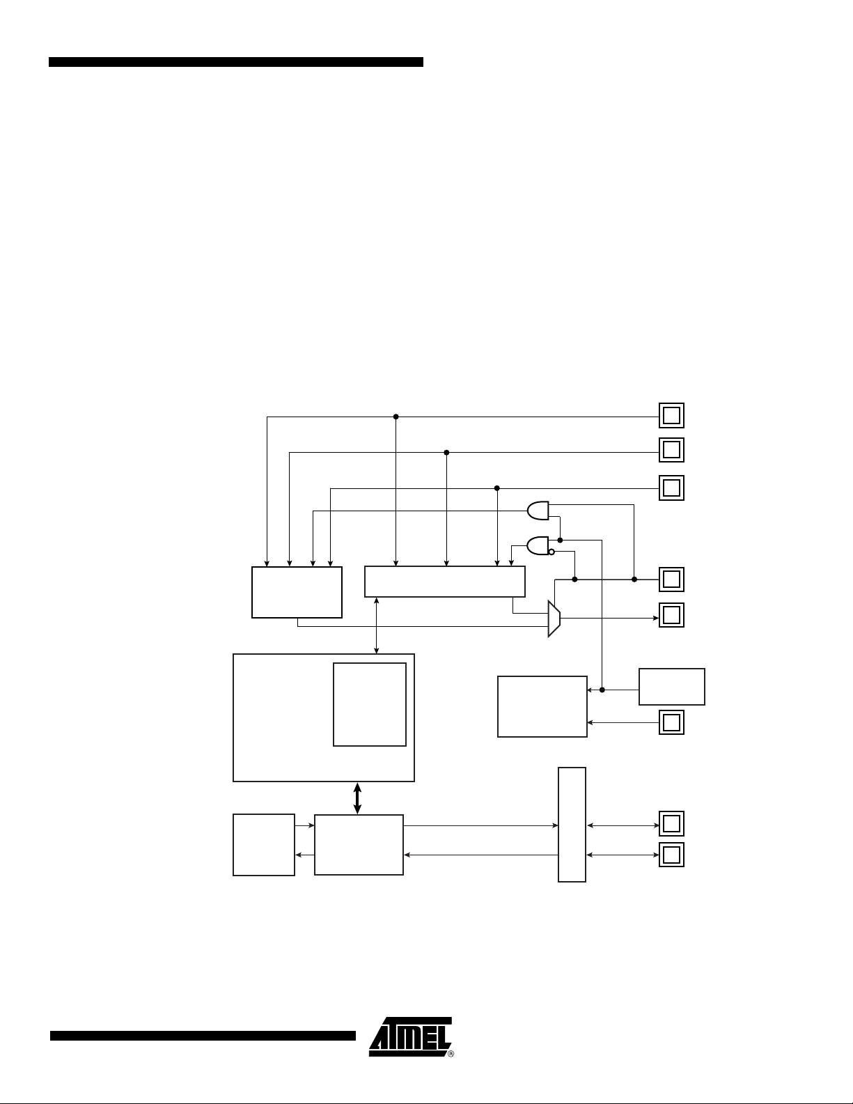
12. Debug and Test Features
12.1 Description
The AT91SAM7S Series Microcontrollers feature a number of complementary debug and test
capabilities. A common JTAG/ICE (EmbeddedICE) port is used for standard debugging functions, such as downloading code and single-stepping through programs. The Debug Unit
provides a two-pin UART that can be used to upload an application into internal SRAM. It manages the interrupt handling of the internal COMMTX and COMMRX signals that trace the activity
of the Debug Communication Channel.
A set of dedicated debug and test input/output pins gives direct access to these capabilities from
a PC-based test environment.
12.2 Block Diagram
Figure 12-1. Debug and Test Block Diagram
AT91SAM7S Series Preliminary
TMS
TCK
PDC
Boundary
TA P
ARM7TDMI
ICE
DBGU
ICE/JTAG
TA P
Reset
and
Test
PIO
TDI
JTAGSEL
TDO
POR
TST
DTXD
DRXD
6175G–ATARM–22-Nov-06
47
Page 48

12.3 Application Examples
12.3.1 Debug Environment
Figure 12-2 on page 48 shows a complete debug environment example. The ICE/JTAG inter-
face is used for standard debugging functions, such as downloading code and single-stepping
through the program.
Figure 12-2. Application Debug Environment Example
Host Debugger
ICE/JTAG
Interface
ICE/JTAG
Connector
AT91SAMS
AT91SAM7S-based Application Board
RS232
Connector
Terminal
48
AT91SAM7S Series Preliminary
6175G–ATARM–22-Nov-06
Page 49

12.3.2 Test Environment
Figure 12-3 on page 49 shows a test environment example. Test vectors are sent and inter-
preted by the tester. In this example, the “board in test” is designed using a number of JTAGcompliant devices. These devices can be connected to form a single scan chain.
Figure 12-3. Application Test Environment Example
AT91SAM7S Series Preliminary
Test Adaptor
JTAG
Interface
ICE/JTAG
Connector
AT91SAM7S
AT91SAM7S-based Application Board In Test
Chip 2Chip n
Chip 1
Tester
6175G–ATARM–22-Nov-06
49
Page 50

12.4 Debug and Test Pin Description
Table 12-1. Debug and Test Pin List
Pin Name Function Type Active Level
NRST Microcontroller Reset Input/Output Low
TST Test Mode Select Input High
TCK Test Clock Input
TDI Test Data In Input
TDO Test Data Out Output
TMS Test Mode Select Input
JTAGSEL JTAG Selection Input
DRXD Debug Receive Data Input
DTXD Debug Transmit Data Output
Reset/Test
ICE and JTAG
Debug Unit
50
AT91SAM7S Series Preliminary
6175G–ATARM–22-Nov-06
Page 51

12.5 Functional Description
12.5.1 Test Pin
One dedicated pin, TST, is used to define the device operating mode. The user must make sure
that this pin is tied at low level to ensure normal operating conditions. Other values associated
with this pin are reserved for manufacturing test.
AT91SAM7S Series Preliminary
12.5.2 EmbeddedICE
12.5.3 Debug Unit
™
(Embedded In-circuit Emulator)
The ARM7TDMI EmbeddedICE is supported via the ICE/JTAG port.The internal state of the
ARM7TDMI is examined through an ICE/JTAG port.
The ARM7TDMI processor contains hardware extensions for advanced debugging features:
• In halt mode, a store-multiple (STM) can be inserted into the instruction pipeline. This exports
the contents of the ARM7TDMI registers. This data can be serially shifted out without
affecting the rest of the system.
• In monitor mode, the JTAG interface is used to transfer data between the debugger and a
simple monitor program running on the ARM7TDMI processor.
There are three scan chains inside the ARM7TDMI processor that support testing, debugging,
and programming of the Embedded ICE. The scan chains are controlled by the ICE/JTAG port.
EmbeddedICE mode is selected when JTAGSEL is low. It is not possible to switch directly
between ICE and JTAG operations. A chip reset must be performed after JTAGSEL is changed.
For further details on the EmbeddedICE, see the ARM7TDMI (Rev4) Technical Reference Manual (DDI0210B).
The Debug Unit provides a two-pin (DXRD and TXRD) USART that can be used for several
debug and trace purposes and offers an ideal means for in-situ programming solutions and
debug monitor communication. Moreover, the association with two peripheral data controller
channels permits packet handling of these tasks with processor time reduced to a minimum.
6175G–ATARM–22-Nov-06
The Debug Unit also manages the interrupt handling of the COMMTX and COMMRX signals
that come from the ICE and that trace the activity of the Debug Communication Channel.The
Debug Unit allows blockage of access to the system through the ICE interface.
A specific register, the Debug Unit Chip ID Register, gives information about the product version
and its internal configuration.
Table 12-2. AT91SAM7S Series Debug Unit Chip ID
Chip Name Chip ID
AT91SAM7S32 0x27080340
AT91SAM7S321 0x27080342
AT91SAM7S64 0x27090540
AT91SAM7S128 0x270A0740
AT91SAM7S256 0x270B0940
AT91SAM7S512 0x270B0A40
51
Page 52

For further details on the Debug Unit, see the Debug Unit section.
12.5.4 IEEE 1149.1 JTAG Boundary Scan
IEEE 1149.1 JTAG Boundary Scan allows pin-level access independent of the device packaging
technology.
IEEE 1149.1 JTAG Boundary Scan is enabled when JTAGSEL is high. The SAMPLE, EXTEST
and BYPASS functions are implemented. In ICE debug mode, the ARM processor responds
with a non-JTAG chip ID that identifies the processor to the ICE system. This is not IEEE 1149.1
JTAG-compliant.
It is not possible to switch directly between JTAG and ICE operations. A chip reset must be performed after JTAGSEL is changed.
A Boundary-scan Descriptor Language (BSDL) file is provided to set up testing.
12.5.4.1 JTAG Boundary-scan Register
The Boundary-scan Register (BSR) contains 96 bits that correspond to active pins and associated control signals.
Each AT91SAM7Sxx input/output pin corresponds to a 3-bit register in the BSR. The OUTPUT
bit contains data that can be forced on the pad. The INPUT bit facilitates the observability of data
applied to the pad. The CONTROL bit selects the direction of the pad.
52
AT91SAM7S Series Preliminary
6175G–ATARM–22-Nov-06
Page 53

AT91SAM7S Series Preliminary
Table 12-3. AT91SAM7Sxx JTAG Boundary Scan Register
Bit Number Pin Name Pin Type
96
Associated BSR
Cells
INPUT
95 OUTPUT
PA17/PGMD5/AD0 IN/OUT
94 CONTROL
93
92 OUTPUT
PA18/PGMD6/AD1 IN/OUT
INPUT
91 CONTROL
90
89 OUTPUT
PA21/PGMD9* IN/OUT*
INPUT
(1)
88 CONTROL
87
86 OUTPUT
PA19/PGMD7/AD2 IN/OUT
INPUT
85 CONTROL
84
83 OUTPUT
PA20/PGMD8/AD3 IN/OUT
INPUT
82 CONTROL
81
80 OUTPUT
PA16/PGMD4 IN/OUT
INPUT
79 CONTROL
78
77 OUTPUT
PA15/PGM3 IN/OUT
INPUT
76 CONTROL
(1)
(1)
6175G–ATARM–22-Nov-06
75
74 OUTPUT
PA14/PGMD2 IN/OUT
INPUT
73 CONTROL
72
71 OUTPUT
PA13/PGMD1 IN/OUT
INPUT
70 CONTROL
69
68 OUTPUT
PA22/PGMD10* IN/OUT*
INPUT
(1)
67 CONTROL
66
65 OUTPUT
PA23/PGMD11* IN/OUT*
INPUT
(1)
64 CONTROL
(1)
(1)
(1)
(1)
53
Page 54

Table 12-3. AT91SAM7Sxx JTAG Boundary Scan Register (Continued)
Bit Number Pin Name Pin Type
63
62 OUTPUT
61 CONTROL
PA24/PGMD12* IN/OUT*
Associated BSR
Cells
(1)
INPUT
(1)
(1)
60
59 OUTPUT
PA12/PGMD0 IN/OUT
INPUT
58 CONTROL
57
56 OUTPUT
PA11/PGMM3 IN/OUT
INPUT
55 CONTROL
54
53 OUTPUT
PA10/PGMM2 IN/OUT
INPUT
52 CONTROL
51
50 OUTPUT
PA9/PGMM1 IN/OUT
INPUT
49 CONTROL
48
47 OUTPUT
PA8/PGMM0 IN/OUT
INPUT
46 CONTROL
45
44 OUTPUT
PA7/PGMNVALID IN/OUT
INPUT
43 CONTROL
54
42
41 OUTPUT
PA6/PGMNOE IN/OUT
40 CONTROL
39
38 OUTPUT
PA5/PGMRDY IN/OUT
37 CONTROL
36
35 OUTPUT
PA4/PGMNCMD IN/OUT
34 CONTROL
33
32 OUTPUT
PA25/PGMD13 IN/OUT
31 CONTROL
AT91SAM7S Series Preliminary
INPUT
INPUT
INPUT
(1)
INPUT
(1)
(1)
6175G–ATARM–22-Nov-06
Page 55

AT91SAM7S Series Preliminary
Table 12-3. AT91SAM7Sxx JTAG Boundary Scan Register (Continued)
Bit Number Pin Name Pin Type
30
29 OUTPUT
28 CONTROL
27
26 OUTPUT
25 CONTROL
24
23 OUTPUT
22 CONTROL
PA26/PGMD14 IN/OUT
PA27/PGMD15 IN/OUT
PA28 IN/OUT
Associated BSR
Cells
(1)
INPUT
(1)
(1)
(1)
INPUT
(1)
(1)
(1)
INPUT
(1)
(1)
21
20 OUTPUT
PA 3 I N/ O UT
INPUT
19 CONTROL
18
17 OUTPUT
PA 2 I N/ O UT
INPUT
16 CONTROL
15
14 OUTPUT
PA1/PGMEN1 IN/OUT
INPUT
13 CONTROL
12
11 OUTPUT
PA0/PGMEN0 IN/OUT
INPUT
10 CONTROL
9
8 OUTPUT
PA29 IN/OUT
INPUT
(1)
7 CONTROL
6
5 OUTPUT
PA30 IN/OUT
INPUT
(1)
4 CONTROL
3
2 OUTPUT
PA31 IN/OUT
INPUT
(1)
1 CONTROL
(1)
(1)
(1)
(1)
(1)
(1)
6175G–ATARM–22-Nov-06
0 ERASE IN INPUT
Note: 1. Does not pertain to AT91SAM7S32.
55
Page 56

12.5.5 ID Code Register
Access: Read-only
31 30 29 28 27 26 25 24
VERSION PART NUMBER
23 22 21 20 19 18 17 16
PART NUMBER
15 14 13 12 11 10 9 8
PART NUMBER MANUFACTURER IDENTITY
76543210
MANUFACTURER IDENTITY 1
• VERSION[31:28]: Product Version Number
Set to 0x0.
• PART NUMBER[27:12]: Product Part Number
Chip Name Chip ID
AT91SAM7S32 0x5B07
AT91SAM7S321 0x5B12
AT91SAM7S64 0x5B06
AT91SAM7S128 0x5B0A
AT91SAM7S256 0x5B09
AT91SAM7S512 0x5B1A
• MANUFACTURER IDENTITY[11:1]
Set to 0x01F.
• Bit[0] Required by IEEE Std. 1149.1.
Set to 0x1.
Chip Name JTAG ID Code
AT91SAM7S32 05B0_703F
AT91SAM7S321 05B1_203F
AT91SAM7S64 05B0_603F
AT91SAM7S128 05B0_A03F
AT91SAM7S256 05B0_903F
AT91SAM7S512 05B1_A03F
56
AT91SAM7S Series Preliminary
6175G–ATARM–22-Nov-06
Page 57

13. Reset Controller (RSTC)
13.1 Overview
The Reset Controller (RSTC), based on power-on reset cells, handles all the resets of the system without any external components. It reports which reset occurred last.
The Reset Controller also drives independently or simultaneously the external reset and the
peripheral and processor resets.
A brownout detection is also available to prevent the processor from falling into an unpredictable
state.
13.2 Block Diagram
Figure 13-1. Reset Controller Block Diagram
AT91SAM7S Series Preliminary
Reset Controller
bod_rst_en
brown_out
Main Supply
POR
NRST
WDRPROC
wd_fault
nrst_out
Brownout
Manager
Startup
Counter
NRST
Manager
bod_reset
user_reset
exter_nreset
Reset
State
Manager
SLCK
rstc_irq
proc_nreset
periph_nreset
6175G–ATARM–22-Nov-06
57
Page 58

13.3 Functional Description
13.3.1 Reset Controller Overview
The Reset Controller is made up of an NRST Manager, a Brownout Manager, a Startup Counter
and a Reset State Manager. It runs at Slow Clock and generates the following reset signals:
• proc_nreset: Processor reset line. It also resets the Watchdog Timer.
• periph_nreset: Affects the whole set of embedded peripherals.
• nrst_out: Drives the NRST pin.
These reset signals are asserted by the Reset Controller, either on external events or on software action. The Reset State Manager controls the generation of reset signals and provides a
signal to the NRST Manager when an assertion of the NRST pin is required.
The NRST Manager shapes the NRST assertion during a programmable time, thus controlling
external device resets.
The startup counter waits for the complete crystal oscillator startup. The wait delay is given by
the crystal oscillator startup time maximum value that can be found in the section Crystal Oscillator Characteristics in the Electrical Characteristics section of the product documentation.
13.3.2 NRST Manager
The NRST Manager samples the NRST input pin and drives this pin low when required by the
Reset State Manager. Figure 13-2 shows the block diagram of the NRST Manager.
Figure 13-2. NRST Manager
13.3.2.1 NRST Signal or Interrupt
The NRST Manager samples the NRST pin at Slow Clock speed. When the line is detected low,
a User Reset is reported to the Reset State Manager.
However, the NRST Manager can be programmed to not trigger a reset when an assertion of
NRST occurs. Writing the bit URSTEN at 0 in RSTC_MR disables the User Reset trigger.
The level of the pin NRST can be read at any time in the bit NRSTL (NRST level) in RSTC_SR.
As soon as the pin NRST is asserted, the bit URSTS in RSTC_SR is set. This bit clears only
when RSTC_SR is read.
NRST
RSTC_SR
URSTS
NRSTL
nrst_out
RSTC_MR
RSTC_MR
URSTEN
RSTC_MR
ERSTL
External Reset Timer
URSTIEN
rstc_irq
Other
interrupt
sources
user_reset
exter_nreset
58
The Reset Controller can also be programmed to generate an interrupt instead of generating a
reset. To do so, the bit URSTIEN in RSTC_MR must be written at 1.
AT91SAM7S Series Preliminary
6175G–ATARM–22-Nov-06
Page 59

13.3.2.2 NRST External Reset Control
The Reset State Manager asserts the signal ext_nreset to assert the NRST pin. When this
occurs, the “nrst_out” signal is driven low by the NRST Manager for a time programmed by the
field ERSTL in RSTC_MR. This assertion duration, named EXTERNAL_RESET_LENGTH, lasts
(ERSTL+1)
2
Slow Clock cycles. This gives the approximate duration of an assertion between 60 µs
and 2 seconds. Note that ERSTL at 0 defines a two-cycle duration for the NRST pulse.
This feature allows the Reset Controller to shape the NRST pin level, and thus to guarantee that
the NRST line is driven low for a time compliant with potential external devices connected on the
system reset.
13.3.3 Brownout Manager
Brownout detection prevents the processor from falling into an unpredictable state if the power
supply drops below a certain level. When VDDCORE drops below the brownout threshold, the
brownout manager requests a brownout reset by asserting the bod_reset signal.
The programmer can disable the brownout reset by setting low the bod_rst_en input signal, i.e.;
by locking the corresponding general-purpose NVM bit in the Flash. When the brownout reset is
disabled, no reset is performed. Instead, the brownout detection is reported in the bit BODSTS
of RSTC_SR. BODSTS is set and clears only when RSTC_SR is read.
AT91SAM7S Series Preliminary
The bit BODSTS can trigger an interrupt if the bit BODIEN is set in the RSTC_MR.
At factory, the brownout reset is disabled.
Figure 13-3. Brownout Manager
bod_rst_en
brown_out
RSTC_SR
BODSTS
RSTC_MR
BODIEN
Other
interrupt
sources
bod_reset
rstc_irq
6175G–ATARM–22-Nov-06
59
Page 60

13.3.4 Reset States
The Reset State Manager handles the different reset sources and generates the internal reset
signals. It reports the reset status in the field RSTTYP of the Status Register (RSTC_SR). The
update of the field RSTTYP is performed when the processor reset is released.
13.3.4.1 Power-up Reset
When VDDCORE is powered on, the Main Supply POR cell output is filtered with a start-up
counter that operates at Slow Clock. The purpose of this counter is to ensure that the Slow
Clock oscillator is stable before starting up the device.
The startup time, as shown in Figure 13-4, is hardcoded to comply with the Slow Clock Oscillator
startup time. After the startup time, the reset signals are released and the field RSTTYP in
RSTC_SR reports a Power-up Reset.
When VDDCORE is detected low by the Main Supply POR Cell, all reset signals are asserted
immediately.
Figure 13-4. Power-up Reset
SLCK
MCK
Main Supply
POR output
proc_nreset
periph_nreset
NRST
(nrst_out)
Startup Time
Processor Startup
= 3 cycles
EXTERNAL RESET LENGTH
= 2 cycles
Any
Freq.
60
AT91SAM7S Series Preliminary
6175G–ATARM–22-Nov-06
Page 61

13.3.4.2 User Reset
The User Reset is entered when a low level is detected on the NRST pin and the bit URSTEN in
RSTC_MR is at 1. The NRST input signal is resynchronized with SLCK to insure proper behavior of the system.
The User Reset is entered as soon as a low level is detected on NRST. The Processor Reset
and the Peripheral Reset are asserted.
The User Reset is left when NRST rises, after a two-cycle resynchronization time and a threecycle processor startup. The processor clock is re-enabled as soon as NRST is confirmed high.
When the processor reset signal is released, the RSTTYP field of the Status Register
(RSTC_SR) is loaded with the value 0x4, indicating a User Reset.
The NRST Manager guarantees that the NRST line is asserted for
EXTERNAL_RESET_LENGTH Slow Clock cycles, as programmed in the field ERSTL. However, if NRST does not rise after EXTERNAL_RESET_LENGTH because it is driven low
externally, the internal reset lines remain asserted until NRST actually rises.
Figure 13-5. User Reset State
AT91SAM7S Series Preliminary
SLCK
MCK
NRST
proc_nreset
RSTTYP
periph_nreset
NRST
(nrst_out)
Any
Freq.
Resynch.
2 cycles
Any XXX
>= EXTERNAL RESET LENGTH
Resynch.
2 cycles
Processor Startup
= 3 cycles
0x4 = User Reset
6175G–ATARM–22-Nov-06
61
Page 62

13.3.4.3 Brownout Reset
When the brown_out/bod_reset signal is asserted, the Reset State Manager immediately enters
the Brownout Reset. In this state, the processor, the peripheral and the external reset lines are
asserted.
The Brownout Reset is left 3 Slow Clock cycles after the rising edge of brown_out/bod_reset
after a two-cycle resynchronization. An external reset is also triggered.
When the processor reset is released, the field RSTTYP in RSTC_SR is loaded with the value
0x5, thus indicating that the last reset is a Brownout Reset.
Figure 13-6. Brownout Reset State
SLCK
MCK
brown_out
or bod_reset
proc_nreset
RSTTYP
periph_nreset
NRST
(nrst_out)
Any
Freq.
Any
Resynch.
2 cycles
XXX
Processor Startup
= 3 cycles
0x5 = Brownout Reset
EXTERNAL RESET LENGTH
8 cycles (ERSTL=2)
62
AT91SAM7S Series Preliminary
6175G–ATARM–22-Nov-06
Page 63

13.3.4.4 Software Reset
The Reset Controller offers several commands used to assert the different reset signals. These
commands are performed by writing the Control Register (RSTC_CR) with the following bits at
1:
The software reset is entered if at least one of these bits is set by the software. All these commands can be performed independently or simultaneously. The software reset lasts 3 Slow
Clock cycles.
The internal reset signals are asserted as soon as the register write is performed. This is
detected on the Master Clock (MCK). They are released when the software reset is left, i.e.; synchronously to SLCK.
If EXTRST is set, the nrst_out signal is asserted depending on the programming of the field
ERSTL. However, the resulting falling edge on NRST does not lead to a User Reset.
AT91SAM7S Series Preliminary
• PROCRST: Writing PROCRST at 1 resets the processor and the watchdog timer.
• PERRST: Writing PERRST at 1 resets all the embedded peripherals, including the memory
system, and, in particular, the Remap Command. The Peripheral Reset is generally used for
debug purposes.
• EXTRST: Writing EXTRST at 1 asserts low the NRST pin during a time defined by the field
ERSTL in the Mode Register (RSTC_MR).
If and only if the PROCRST bit is set, the Reset Controller reports the software status in the field
RSTTYP of the Status Register (RSTC_SR). Other Software Resets are not reported in
RSTTYP.
As soon as a software operation is detected, the bit SRCMP (Software Reset Command in
Progress) is set in the Status Register (RSTC_SR). It is cleared as soon as the software reset is
left. No other software reset can be performed while the SRCMP bit is set, and writing any value
in RSTC_CR has no effect.
Figure 13-7. Software Reset
SLCK
MCK
Write RSTC_CR
proc_nreset
if PROCRST=1
RSTTYP
periph_nreset
if PERRST=1
Any
Freq.
Any
Resynch.
1 cycle
Processor Startup
= 3 cycles
XXX
0x3 = Software Reset
6175G–ATARM–22-Nov-06
NRST
(nrst_out)
if EXTRST=1
SRCMP in RSTC_SR
EXTERNAL RESET LENGTH
8 cycles (ERSTL=2)
63
Page 64

13.3.4.5 Watchdog Reset
The Watchdog Reset is entered when a watchdog fault occurs. This state lasts 3 Slow Clock
cycles.
When in Watchdog Reset, assertion of the reset signals depends on the WDRPROC bit in
WDT_MR:
• If WDRPROC is 0, the Processor Reset and the Peripheral Reset are asserted. The NRST
• If WDRPROC = 1, only the processor reset is asserted.
The Watchdog Timer is reset by the proc_nreset signal. As the watchdog fault always causes a
processor reset if WDRSTEN is set, the Watchdog Timer is always reset after a Watchdog
Reset, and the Watchdog is enabled by default and with a period set to a maximum.
When the WDRSTEN in WDT_MR bit is reset, the watchdog fault has no impact on the reset
controller.
Figure 13-8. Watchdog Reset
line is also asserted, depending on the programming of the field ERSTL. However, the
resulting low level on NRST does not result in a User Reset state.
SLCK
Only if
WDRPROC = 0
MCK
wd_fault
proc_nreset
RSTTYP
periph_nreset
NRST
(nrst_out)
Any
Freq.
Any
Processor Startup
= 3 cycles
XXX
EXTERNAL RESET LENGTH
0x2 = Watchdog Reset
8 cycles (ERSTL=2)
64
AT91SAM7S Series Preliminary
6175G–ATARM–22-Nov-06
Page 65

13.3.5 Reset State Priorities
The Reset State Manager manages the following priorities between the different reset sources,
given in descending order:
• Power-up Reset
•Brownout Reset
• Watchdog Reset
• Software Reset
• User Reset
Particular cases are listed below:
• When in User Reset:
• When in Software Reset:
• When in Watchdog Reset:
AT91SAM7S Series Preliminary
– A watchdog event is impossible because the Watchdog Timer is being reset by the
proc_nreset signal.
– A software reset is impossible, since the processor reset is being activated.
– A watchdog event has priority over the current state.
– The NRST has no effect.
– The processor reset is active and so a Software Reset cannot be programmed.
– A User Reset cannot be entered.
13.3.6 Reset Controller Status Register
The Reset Controller status register (RSTC_SR) provides several status fields:
• RSTTYP field: This field gives the type of the last reset, as explained in previous sections.
• SRCMP bit: This field indicates that a Software Reset Command is in progress and that no
further software reset should be performed until the end of the current one. This bit is
automatically cleared at the end of the current software reset.
• NRSTL bit: The NRSTL bit of the Status Register gives the level of the NRST pin sampled on
each MCK rising edge.
• URSTS bit: A high-to-low transition of the NRST pin sets the URSTS bit of the RSTC_SR
register. This transition is also detected on the Master Clock (MCK) rising edge (see Figure
13-9). If the User Reset is disabled (URSTEN = 0) and if the interruption is enabled by the
URSTIEN bit in the RSTC_MR register, the URSTS bit triggers an interrupt. Reading the
RSTC_SR status register resets the URSTS bit and clears the interrupt.
• BODSTS bit: This bit indicates a brownout detection when the brownout reset is disabled
(bod_rst_en = 0). It triggers an interrupt if the bit BODIEN in the RSTC_MR register enables
the interrupt. Reading the RSTC_SR register resets the BODSTS bit and clears the interrupt.
6175G–ATARM–22-Nov-06
65
Page 66

Figure 13-9. Reset Controller Status and Interrupt
MCK
Peripheral Access
NRST
NRSTL
URSTS
rstc_irq
if (URSTEN = 0) and
(URSTIEN = 1)
2 cycle
resynchronization
read
RSTC_SR
2 cycle
resynchronization
66
AT91SAM7S Series Preliminary
6175G–ATARM–22-Nov-06
Page 67

AT91SAM7S Series Preliminary
13.4 Reset Controller (RSTC) User Interface
Table 13-1. Reset Controller (RSTC) Register Mapping
Offset Register Name Access Reset Value
0x00 Control Register RSTC_CR Write-only -
0x04 Status Register RSTC_SR Read-only 0x0000_0000
0x08 Mode Register RSTC_MR Read/Write 0x0000_0000
6175G–ATARM–22-Nov-06
67
Page 68

13.4.1 Reset Controller Control Register Register Name: RSTC_CR Access Type: Write-only
31 30 29 28 27 26 25 24
KEY
23 22 21 20 19 18 17 16
––––––––
15 14 13 12 11 10 9 8
––––––––
76543210
––––EXTRSTPERRST–PROCRST
• PROCRST: Processor Reset
0 = No effect.
1 = If KEY is correct, resets the processor.
• PERRST: Peripheral Reset
0 = No effect.
1 = If KEY is correct, resets the peripherals.
• EXTRST: External Reset
0 = No effect.
1 = If KEY is correct, asserts the NRST pin.
•KEY: Password
Should be written at value 0xA5. Writing any other value in this field aborts the write operation.
68
AT91SAM7S Series Preliminary
6175G–ATARM–22-Nov-06
Page 69

AT91SAM7S Series Preliminary
13.4.2 Reset Controller Status Register Register Name: RSTC_SR Access Type: Read-only
31 30 29 28 27 26 25 24
––––––––
23 22 21 20 19 18 17 16
––––––SRCMPNRSTL
15 14 13 12 11 10 9 8
––––– RSTTYP
76543210
––––––BODSTSURSTS
• URSTS: User Reset Status
0 = No high-to-low edge on NRST happened since the last read of RSTC_SR.
1 = At least one high-to-low transition of NRST has been detected since the last read of RSTC_SR.
• BODSTS: Brownout Detection Status
0 = No brownout high-to-low transition happened since the last read of RSTC_SR.
1 = A brownout high-to-low transition has been detected since the last read of RSTC_SR.
• RSTTYP: Reset Type
Reports the cause of the last processor reset. Reading this RSTC_SR does not reset this field.
RSTTYP Reset Type Comments
0 0 0 Power-up Reset VDDCORE rising
0 1 0 Watchdog Reset Watchdog fault occurred
0 1 1 Software Reset Processor reset required by the software
1 0 0 User Reset NRST pin detected low
1 0 1 Brownout Reset BrownOut reset occurred
• NRSTL: NRST Pin Level
Registers the NRST Pin Level at Master Clock (MCK).
• SRCMP: Software Reset Command in Progress
0 = No software command is being performed by the reset controller. The reset controller is ready for a software command.
1 = A software reset command is being performed by the reset controller. The reset controller is busy.
69
6175G–ATARM–22-Nov-06
Page 70

13.4.3 Reset Controller Mode Register Register Name: RSTC_MR Access Type: Read/Write
31 30 29 28 27 26 25 24
KEY
23 22 21 20 19 18 17 16
–––––––BODIEN
15 14 13 12 11 10 9 8
–––– ERSTL
76543210
–––URSTIEN–––URSTEN
• URSTEN: User Reset Enable
0 = The detection of a low level on the pin NRST does not generate a User Reset.
1 = The detection of a low level on the pin NRST triggers a User Reset.
• URSTIEN: User Reset Interrupt Enable
0 = USRTS bit in RSTC_SR at 1 has no effect on rstc_irq.
1 = USRTS bit in RSTC_SR at 1 asserts rstc_irq if URSTEN = 0.
• BODIEN: Brownout Detection Interrupt Enable
0 = BODSTS bit in RSTC_SR at 1 has no effect on rstc_irq.
1 = BODSTS bit in RSTC_SR at 1 asserts rstc_irq.
• ERSTL: External Reset Length
This field defines the external reset length. The external reset is asserted during a time of 2
(ERSTL+1)
allows assertion duration to be programmed between 60 µs and 2 seconds.
•KEY: Password
Should be written at value 0xA5. Writing any other value in this field aborts the write operation.
Slow Clock cycles. This
70
AT91SAM7S Series Preliminary
6175G–ATARM–22-Nov-06
Page 71

AT91SAM7S Series Preliminary
6175G–ATARM–22-Nov-06
71
Page 72

72
AT91SAM7S Series Preliminary
6175G–ATARM–22-Nov-06
Page 73

14. Real-time Timer (RTT)
14.1 Overview
The Real-time Timer is built around a 32-bit counter and used to count elapsed seconds. It generates a periodic interrupt or/and triggers an alarm on a programmed value.
14.2 Block Diagram
Figure 14-1. Real-time Timer
AT91SAM7S Series Preliminary
SLCK
RTT_MR
RTTRST
reload
16-bit
Divider
RTT_MR
RTPRES
RTT_MR
RTTRST
RTT_VR
RTT_AR
0
10
32-bit
Counter
CRTV
ALMV
RTT_SR
RTT_SR
RTT_SR
=
read
set
reset
reset
set
RTT_MR
RTTINCIEN
RTTINC
rtt_int
RTT_MR
ALMIEN
ALMS
rtt_alarm
14.3 Functional Description
The Real-time Timer is used to count elapsed seconds. It is built around a 32-bit counter fed by
Slow Clock divided by a programmable 16-bit value. The value can be programmed in the field
RTPRES of the Real-time Mode Register (RTT_MR).
Programming RTPRES at 0x00008000 corresponds to feeding the real-time counter with a 1 Hz
signal (if the Slow Clock is 32.768 Hz). The 32-bit counter can count up to 2
sponding to more than 136 years, then roll over to 0.
The Real-time Timer can also be used as a free-running timer with a lower time-base. The best
accuracy is achieved by writing RTPRES to 3. Programming RTPRES to 1 or 2 is possible, but
may result in losing status events because the status register is cleared two Slow Clock cycles
after read. Thus if the RTT is configured to trigger an interrupt, the interrupt occurs during 2 Slow
Clock cycles after reading RTT_SR. To prevent several executions of the interrupt handler, the
interrupt must be disabled in the interrupt handler and re-enabled when the status register is
clear.
6175G–ATARM–22-Nov-06
32
seconds, corre-
73
Page 74

The Real-time Timer value (CRTV) can be read at any time in the register RTT_VR (Real-time
Value Register). As this value can be updated asynchronously from the Master Clock, it is advisable to read this register twice at the same value to improve accuracy of the returned value.
The current value of the counter is compared with the value written in the alarm register
RTT_AR (Real-time Alarm Register). If the counter value matches the alarm, the bit ALMS in
RTT_SR is set. The alarm register is set to its maximum value, corresponding to 0xFFFF_FFFF,
after a reset.
The bit RTTINC in RTT_SR is set each time the Real-time Timer counter is incremented. This bit
can be used to start a periodic interrupt, the period being one second when the RTPRES is programmed with 0x8000 and Slow Clock equal to 32.768 Hz.
Reading the RTT_SR status register resets the RTTINC and ALMS fields.
Writing the bit RTTRST in RTT_MR immediately reloads and restarts the clock divider with the
new programmed value. This also resets the 32-bit counter.
Note: Because of the asynchronism between the Slow Clock (SCLK) and the System Clock (MCK):
1) The restart of the counter and the reset of the RTT_VR current value register is effective only 2
slow clock cycles after the write of the RTTRST bit in the RTT_MR register.
2) The status register flags reset is taken into account only 2 slow clock cycles after the read of the
RTT_SR (Status Register).
Figure 14-2. RTT Counting
MCK
RTPRES - 1
Prescaler
RTT
RTTINC (RTT_SR)
ALMS (RTT_SR)
APB Interface
APB cycle
0
...
ALMVALMV-10 ALMV+1
read RTT_SR
ALMV+2 ALMV+3
APB cycle
74
AT91SAM7S Series Preliminary
6175G–ATARM–22-Nov-06
Page 75

AT91SAM7S Series Preliminary
14.4 Real-time Timer (RTT) User Interface
Table 14-1. Real-time Timer (RTT) Register Mapping
Offset Register Name Access Reset Value
0x00 Mode Register RTT_MR Read/Write 0x0000_8000
0x04 Alarm Register RTT_AR Read/Write 0xFFFF_FFFF
0x08 Value Register RTT_VR Read-only 0x0000_0000
0x0C Status Register RTT_SR Read-only 0x0000_0000
6175G–ATARM–22-Nov-06
75
Page 76

14.4.1 Real-time Timer Mode Register Register Name: RTT_MR Access Type: Read/Write
31 30 29 28 27 26 25 24
––––––––
23 22 21 20 19 18 17 16
–––––RTTRSTRTTINCIENALMIEN
15 14 13 12 11 10 9 8
RTPRES
76543210
RTPRES
• RTPRES: Real-time Timer Prescaler Value
Defines the number of SLCK periods required to increment the real-time timer. RTPRES is defined as follows:
RTPRES = 0: The Prescaler Period is equal to 2
16
RTPRES ≠ 0: The Prescaler Period is equal to RTPRES.
• ALMIEN: Alarm Interrupt Enable
0 = The bit ALMS in RTT_SR has no effect on interrupt.
1 = The bit ALMS in RTT_SR asserts interrupt.
• RTTINCIEN: Real-time Timer Increment Interrupt Enable
0 = The bit RTTINC in RTT_SR has no effect on interrupt.
1 = The bit RTTINC in RTT_SR asserts interrupt.
• RTTRST: Real-time Timer Restart
1 = Reloads and restarts the clock divider with the new programmed value. This also resets the 32-bit counter.
76
AT91SAM7S Series Preliminary
6175G–ATARM–22-Nov-06
Page 77

AT91SAM7S Series Preliminary
14.4.2 Real-time Timer Alarm Register Register Name: RTT_AR Access Type: Read/Write
31 30 29 28 27 26 25 24
ALMV
23 22 21 20 19 18 17 16
ALMV
15 14 13 12 11 10 9 8
ALMV
76543210
ALMV
• ALMV: Alarm Value
Defines the alarm value (ALMV+1) compared with the Real-time Timer.
14.4.3 Real-time Timer Value Register Register Name: RTT_VR Access Type: Read-only
31 30 29 28 27 26 25 24
CRTV
23 22 21 20 19 18 17 16
CRTV
15 14 13 12 11 10 9 8
CRTV
76543210
CRTV
• CRTV: Current Real-time Value
Returns the current value of the Real-time Timer.
6175G–ATARM–22-Nov-06
77
Page 78

14.4.4 Real-time Timer Status Register Register Name: RTT_SR Access Type: Read-only
31 30 29 28 27 26 25 24
––––––––
23 22 21 20 19 18 17 16
––––––––
15 14 13 12 11 10 9 8
––––––––
76543210
––––––RTTINCALMS
• ALMS: Real-time Alarm Status
0 = The Real-time Alarm has not occurred since the last read of RTT_SR.
1 = The Real-time Alarm occurred since the last read of RTT_SR.
• RTTINC: Real-time Timer Increment
0 = The Real-time Timer has not been incremented since the last read of the RTT_SR.
1 = The Real-time Timer has been incremented since the last read of the RTT_SR.
78
AT91SAM7S Series Preliminary
6175G–ATARM–22-Nov-06
Page 79

15. Parallel Input Output Controller (PIO)
15.1 Overview
The Parallel Input/Output Controller (PIO) manages up to 32 fully programmable input/output
lines. Each I/O line may be dedicated as a general-purpose I/O or be assigned to a function of
an embedded peripheral. This assures effective optimization of the pins of a product.
Each I/O line is associated with a bit number in all of the 32-bit registers of the 32-bit wide User
Interface.
Each I/O line of the PIO Controller features:
• An input change interrupt enabling level change detection on any I/O line.
• A glitch filter providing rejection of pulses lower than one-half of clock cycle.
• Multi-drive capability similar to an open drain I/O line.
• Control of the pull-up of the I/O line.
• Input visibility and output control.
The PIO Controller also features a synchronous output providing up to 32 bits of data output in a
single write operation.
AT91SAM7S Series Preliminary
6175G–ATARM–22-Nov-06
79
Page 80

15.2 Block Diagram
Figure 15-1. Block Diagram
PIO Controller
AIC
PMC
Embedded
Peripheral
Embedded
Peripheral
PIO Interrupt
PIO Clock
Data, Enable
Data, Enable
Up to 32
peripheral IOs
Up to 32
peripheral IOs
PIN 0
PIN 1
PIN 31
Up to 32 pins
Figure 15-2. Application Block Diagram
Keyboard Driver
Keyboard Driver General Purpose I/Os External Devices
80
AT91SAM7S Series Preliminary
Control & Command
Driver
PIO Controller
APB
On-Chip Peripheral Drivers
On-Chip Peripherals
6175G–ATARM–22-Nov-06
Page 81

15.3 Product Dependencies
15.3.1 Pin Multiplexing
Each pin is configurable, according to product definition as either a general-purpose I/O line
only, or as an I/O line multiplexed with one or two peripheral I/Os. As the multiplexing is hardware-defined and thus product-dependent, the hardware designer and programmer must
carefully determine the configuration of the PIO controllers required by their application. When
an I/O line is general-purpose only, i.e. not multiplexed with any peripheral I/O, programming of
the PIO Controller regarding the assignment to a peripheral has no effect and only the PIO Controller can control how the pin is driven by the product.
15.3.2 External Interrupt Lines
The interrupt signals FIQ and IRQ0 to IRQn are most generally multiplexed through the PIO
Controllers. However, it is not necessary to assign the I/O line to the interrupt function as the
PIO Controller has no effect on inputs and the interrupt lines (FIQ or IRQs) are used only as
inputs.
15.3.3 Power Management
The Power Management Controller controls the PIO Controller clock in order to save power.
Writing any of the registers of the user interface does not require the PIO Controller clock to be
enabled. This means that the configuration of the I/O lines does not require the PIO Controller
clock to be enabled.
AT91SAM7S Series Preliminary
However, when the clock is disabled, not all of the features of the PIO Controller are available.
Note that the Input Change Interrupt and the read of the pin level require the clock to be
validated.
After a hardware reset, the PIO clock is disabled by default.
The user must configure the Power Management Controller before any access to the input line
information.
15.3.4 Interrupt Generation
For interrupt handling, the PIO Controllers are considered as user peripherals. This means that
the PIO Controller interrupt lines are connected among the interrupt sources 2 to 31. Refer to the
PIO Controller peripheral identifier in the product description to identify the interrupt sources
dedicated to the PIO Controllers.
The PIO Controller interrupt can be generated only if the PIO Controller clock is enabled.
6175G–ATARM–22-Nov-06
81
Page 82

15.4 Functional Description
The PIO Controller features up to 32 fully-programmable I/O lines. Most of the control logic associated to each I/O is represented in Figure 15-3. In this description each signal shown
represents but one of up to 32 possible indexes.
Figure 15-3. I/O Line Control Logic
PIO_OER[0]
PIO_OSR[0]
PIO_ODR[0]
Peripheral A
Output Enable
Peripheral B
Output Enable
PIO_ASR[0]
PIO_ABSR[0]
PIO_BSR[0]
Peripheral A
Output
Peripheral B
Output
0
1
0
1
PIO_PER[0]
PIO_PSR[0]
PIO_PDR[0]
PIO_SODR[0]
PIO_ODSR[0]
PIO_CODR[0]
PIO_PUER[0]
PIO_PUSR[0]
1
0
PIO_MDER[0]
PIO_MDSR[0]
0
1
PIO_MDDR[0]
PIO_PUDR[0]
0
1
0
Pad
1
PIO_IFER[0]
PIO_IFSR[0]
PIO_IFDR[0]
Glitch
Filter
PIO_PDSR[0] PIO_ISR[0]
0
Edge
Detector
1
PIO_IER[0]
PIO_IMR[0]
PIO_IDR[0]
PIO_ISR[31]
PIO_IER[31]
PIO_IMR[31]
PIO_IDR[31]
Peripheral A
Input
Peripheral B
Input
(Up to 32 possible inputs)
PIO Interrupt
82
AT91SAM7S Series Preliminary
6175G–ATARM–22-Nov-06
Page 83

15.4.1 Pull-up Resistor Control
Each I/O line is designed with an embedded pull-up resistor. The pull-up resistor can be enabled
or disabled by writing respectively PIO_PUER (Pull-up Enable Register) and PIO_PUDR (Pullup Disable Resistor). Writing in these registers results in setting or clearing the corresponding bit
in PIO_PUSR (Pull-up Status Register). Reading a 1 in PIO_PUSR means the pull-up is disabled and reading a 0 means the pull-up is enabled.
Control of the pull-up resistor is possible regardless of the configuration of the I/O line.
After reset, all of the pull-ups are enabled, i.e. PIO_PUSR resets at the value 0x0.
15.4.2 I/O Line or Peripheral Function Selection
When a pin is multiplexed with one or two peripheral functions, the selection is controlled with
the registers PIO_PER (PIO Enable Register) and PIO_PDR (PIO Disable Register). The register PIO_PSR (PIO Status Register) is the result of the set and clear registers and indicates
whether the pin is controlled by the corresponding peripheral or by the PIO Controller. A value of
0 indicates that the pin is controlled by the corresponding on-chip peripheral selected in the
PIO_ABSR (AB Select Status Register). A value of 1 indicates the pin is controlled by the PIO
controller.
If a pin is used as a general purpose I/O line (not multiplexed with an on-chip peripheral),
PIO_PER and PIO_PDR have no effect and PIO_PSR returns 1 for the corresponding bit.
AT91SAM7S Series Preliminary
After reset, most generally, the I/O lines are controlled by the PIO controller, i.e. PIO_PSR
resets at 1. However, in some events, it is important that PIO lines are controlled by the peripheral (as in the case of memory chip select lines that must be driven inactive after reset or for
address lines that must be driven low for booting out of an external memory). Thus, the reset
value of PIO_PSR is defined at the product level, depending on the multiplexing of the device.
15.4.3 Peripheral A or B Selection
The PIO Controller provides multiplexing of up to two peripheral functions on a single pin. The
selection is performed by writing PIO_ASR (A Select Register) and PIO_BSR (Select B Register). PIO_ABSR (AB Select Status Register) indicates which peripheral line is currently selected.
For each pin, the corresponding bit at level 0 means peripheral A is selected whereas the corresponding bit at level 1 indicates that peripheral B is selected.
Note that multiplexing of peripheral lines A and B only affects the output line. The peripheral
input lines are always connected to the pin input.
After reset, PIO_ABSR is 0, thus indicating that all the PIO lines are configured on peripheral A.
However, peripheral A generally does not drive the pin as the PIO Controller resets in I/O line
mode.
Writing in PIO_ASR and PIO_BSR manages PIO_ABSR regardless of the configuration of the
pin. However, assignment of a pin to a peripheral function requires a write in the corresponding
peripheral selection register (PIO_ASR or PIO_BSR) in addition to a write in PIO_PDR.
15.4.4 Output Control
6175G–ATARM–22-Nov-06
When the I/0 line is assigned to a peripheral function, i.e. the corresponding bit in PIO_PSR is at
0, the drive of the I/O line is controlled by the peripheral. Peripheral A or B, depending on the
value in PIO_ABSR, determines whether the pin is driven or not.
83
Page 84

When the I/O line is controlled by the PIO controller, the pin can be configured to be driven. This
is done by writing PIO_OER (Output Enable Register) and PIO_ODR (Output Disable Register).
The results of these write operations are detected in PIO_OSR (Output Status Register). When
a bit in this register is at 0, the corresponding I/O line is used as an input only. When the bit is at
1, the corresponding I/O line is driven by the PIO controller.
The level driven on an I/O line can be determined by writing in PIO_SODR (Set Output Data
Register) and PIO_CODR (Clear Output Data Register). These write operations respectively set
and clear PIO_ODSR (Output Data Status Register), which represents the data driven on the I/O
lines. Writing in PIO_OER and PIO_ODR manages PIO_OSR whether the pin is configured to
be controlled by the PIO controller or assigned to a peripheral function. This enables configuration of the I/O line prior to setting it to be managed by the PIO Controller.
Similarly, writing in PIO_SODR and PIO_CODR effects PIO_ODSR. This is important as it
defines the first level driven on the I/O line.
15.4.5 Synchronous Data Output
Controlling all parallel busses using several PIOs requires two successive write operations in the
PIO_SODR and PIO_CODR registers. This may lead to unexpected transient values. The PIO
controller offers a direct control of PIO outputs by single write access to PIO_ODSR (Output
Data Status Register). Only bits unmasked by PIO_OSWSR (Output Write Status Register) are
written. The mask bits in the PIO_OWSR are set by writing to PIO_OWER (Output Write Enable
Register) and cleared by writing to PIO_OWDR (Output Write Disable Register).
After reset, the synchronous data output is disabled on all the I/O lines as PIO_OWSR resets at
0x0.
15.4.6 Multi Drive Control (Open Drain)
Each I/O can be independently programmed in Open Drain by using the Multi Drive feature. This
feature permits several drivers to be connected on the I/O line which is driven low only by each
device. An external pull-up resistor (or enabling of the internal one) is generally required to guarantee a high level on the line.
The Multi Drive feature is controlled by PIO_MDER (Multi-driver Enable Register) and
PIO_MDDR (Multi-driver Disable Register). The Multi Drive can be selected whether the I/O line
is controlled by the PIO controller or assigned to a peripheral function. PIO_MDSR (Multi-driver
Status Register) indicates the pins that are configured to support external drivers.
After reset, the Multi Drive feature is disabled on all pins, i.e. PIO_MDSR resets at value 0x0.
15.4.7 Output Line Timings
Figure 15-4 shows how the outputs are driven either by writing PIO_SODR or PIO_CODR, or by
directly writing PIO_ODSR. This last case is valid only if the corresponding bit in PIO_OWSR is
set. Figure 15-4 also shows when the feedback in PIO_PDSR is available.
84
AT91SAM7S Series Preliminary
6175G–ATARM–22-Nov-06
Page 85

Figure 15-4. Output Line Timings
MCK
AT91SAM7S Series Preliminary
Write PIO_SODR
Write PIO_ODSR at 1
Write PIO_CODR
Write PIO_ODSR at 0
PIO_ODSR
PIO_PDSR
15.4.8 Inputs
The level on each I/O line can be read through PIO_PDSR (Pin Data Status Register). This register indicates the level of the I/O lines regardless of their configuration, whether uniquely as an
input or driven by the PIO controller or driven by a peripheral.
Reading the I/O line levels requires the clock of the PIO controller to be enabled, otherwise
PIO_PDSR reads the levels present on the I/O line at the time the clock was disabled.
15.4.9 Input Glitch Filtering
Optional input glitch filters are independently programmable on each I/O line. When the glitch filter is enabled, a glitch with a duration of less than 1/2 Master Clock (MCK) cycle is automatically
rejected, while a pulse with a duration of 1 Master Clock cycle or more is accepted. For pulse
durations between 1/2 Master Clock cycle and 1 Master Clock cycle the pulse may or may not
be taken into account, depending on the precise timing of its occurrence. Thus for a pulse to be
visible it must exceed 1 Master Clock cycle, whereas for a glitch to be reliably filtered out, its
duration must not exceed 1/2 Master Clock cycle. The filter introduces one Master Clock cycle
latency if the pin level change occurs before a rising edge. However, this latency does not
appear if the pin level change occurs before a falling edge. This is illustrated in Figure 15-5.
APB Access
2 cycles
APB Access
2 cycles
6175G–ATARM–22-Nov-06
The glitch filters are controlled by the register set; PIO_IFER (Input Filter Enable Register),
PIO_IFDR (Input Filter Disable Register) and PIO_IFSR (Input Filter Status Register). Writing
PIO_IFER and PIO_IFDR respectively sets and clears bits in PIO_IFSR. This last register
enables the glitch filter on the I/O lines.
When the glitch filter is enabled, it does not modify the behavior of the inputs on the peripherals.
It acts only on the value read in PIO_PDSR and on the input change interrupt detection. The
glitch filters require that the PIO Controller clock is enabled.
85
Page 86

Figure 15-5. Input Glitch Filter Timing
MCK
Pin Level
1 cycle 1 cycle 1 cycle
PIO_PDSR
if PIO_IFSR = 0
up to 1.5 cycles
2 cycles
1 cycle
1 cycle
PIO_PDSR
if PIO_IFSR = 1
15.4.10 Input Change Interrupt
The PIO Controller can be programmed to generate an interrupt when it detects an input change
on an I/O line. The Input Change Interrupt is controlled by writing PIO_IER (Interrupt Enable
Register) and PIO_IDR (Interrupt Disable Register), which respectively enable and disable the
input change interrupt by setting and clearing the corresponding bit in PIO_IMR (Interrupt Mask
Register). As Input change detection is possible only by comparing two successive samplings of
the input of the I/O line, the PIO Controller clock must be enabled. The Input Change Interrupt is
available, regardless of the configuration of the I/O line, i.e. configured as an input only, controlled by the PIO Controller or assigned to a peripheral function.
When an input change is detected on an I/O line, the corresponding bit in PIO_ISR (Interrupt
Status Register) is set. If the corresponding bit in PIO_IMR is set, the PIO Controller interrupt
line is asserted. The interrupt signals of the thirty-two channels are ORed-wired together to generate a single interrupt signal to the Advanced Interrupt Controller.
When the software reads PIO_ISR, all the interrupts are automatically cleared. This signifies that
all the interrupts that are pending when PIO_ISR is read must be handled.
Figure 15-6. Input Change Interrupt Timings
up to 2.5 cycles up to 2 cycles
Read PIO_ISR
86
MCK
Pin Level
PIO_ISR
APB Access
AT91SAM7S Series Preliminary
APB Access
6175G–ATARM–22-Nov-06
Page 87

15.5 I/O Lines Programming Example
The programing example as shown in Table 15-1 below is used to define the following
configuration.
• 4-bit output port on I/O lines 0 to 3, (should be written in a single write operation), open-drain,
with pull-up resistor
• Four output signals on I/O lines 4 to 7 (to drive LEDs for example), driven high and low, no
pull-up resistor
• Four input signals on I/O lines 8 to 11 (to read push-button states for example), with pull-up
resistors, glitch filters and input change interrupts
• Four input signals on I/O line 12 to 15 to read an external device status (polled, thus no input
change interrupt), no pull-up resistor, no glitch filter
• I/O lines 16 to 19 assigned to peripheral A functions with pull-up resistor
• I/O lines 20 to 23 assigned to peripheral B functions, no pull-up resistor
• I/O line 24 to 27 assigned to peripheral A with Input Change Interrupt and pull-up resistor
Table 15-1. Programming Example
Register Value to be Written
PIO_PER 0x0000 FFFF
AT91SAM7S Series Preliminary
PIO_PDR 0x0FFF 0000
PIO_OER 0x0000 00FF
PIO_ODR 0x0FFF FF00
PIO_IFER 0x0000 0F00
PIO_IFDR 0x0FFF F0FF
PIO_SODR 0x0000 0000
PIO_CODR 0x0FFF FFFF
PIO_IER 0x0F00 0F00
PIO_IDR 0x00FF F0FF
PIO_MDER 0x0000 000F
PIO_MDDR 0x0FFF FFF0
PIO_PUDR 0x00F0 00F0
PIO_PUER 0x0F0F FF0F
PIO_ASR 0x0F0F 0000
PIO_BSR 0x00F0 0000
PIO_OWER 0x0000 000F
PIO_OWDR 0x0FFF FFF0
6175G–ATARM–22-Nov-06
87
Page 88

15.6 User Interface
Each I/O line controlled by the PIO Controller is associated with a bit in each of the PIO Controller User Interface registers. Each register is 32 bits wide. If a parallel I/O line is not defined,
writing to the corresponding bits has no effect. Undefined bits read zero. If the I/O line is not multiplexed with any peripheral, the I/O line is controlled by the PIO Controller and PIO_PSR returns
1 systematically.
Table 15-2. Register Mapping
Offset Register Name Access Reset Value
0x0000 PIO Enable Register PIO_PER Write-only –
0x0004 PIO Disable Register PIO_PDR Write-only –
0x0008 PIO Status Register
0x000C Reserved
0x0010 Output Enable Register PIO_OER Write-only –
0x0014 Output Disable Register PIO_ODR Write-only –
0x0018 Output Status Register PIO_OSR Read-only 0x0000 0000
0x001C Reserved
0x0020 Glitch Input Filter Enable Register PIO_IFER Write-only –
(1)
PIO_PSR Read-only 0x0000 0000
0x0024 Glitch Input Filter Disable Register PIO_IFDR Write-only –
0x0028 Glitch Input Filter Status Register PIO_IFSR Read-only 0x0000 0000
0x002C Reserved
0x0030 Set Output Data Register PIO_SODR Write-only –
0x0034 Clear Output Data Register PIO_CODR Write-only –
0x0038 Output Data Status Register
0x003C Pin Data Status Register
0x0040 Interrupt Enable Register PIO_IER Write-only –
0x0044 Interrupt Disable Register PIO_IDR Write-only –
0x0048 Interrupt Mask Register PIO_IMR Read-only 0x00000000
0x004C Interrupt Status Register
0x0050 Multi-driver Enable Register PIO_MDER Write-only –
0x0054 Multi-driver Disable Register PIO_MDDR Write-only –
0x0058 Multi-driver Status Register PIO_MDSR Read-only 0x00000000
0x005C Reserved
0x0060 Pull-up Disable Register PIO_PUDR Write-only –
0x0064 Pull-up Enable Register PIO_PUER Write-only –
0x0068 Pad Pull-up Status Register PIO_PUSR Read-only 0x00000000
0x006C Reserved
(2)
(3)
(4)
PIO_ODSR Read-only 0x0000 0000
PIO_PDSR Read-only
PIO_ISR Read-only 0x00000000
88
AT91SAM7S Series Preliminary
6175G–ATARM–22-Nov-06
Page 89

AT91SAM7S Series Preliminary
Table 15-2. Register Mapping (Continued)
Offset Register Name Access Reset Value
0x0070 Peripheral A Select Register
0x0074 Peripheral B Select Register
0x0078 AB Status Register
0x007C
to
0x009C
0x00A0 Output Write Enable PIO_OWER Write-only –
0x00A4 Output Write Disable PIO_OWDR Write-only –
0x00A8 Output Write Status Register PIO_OWSR Read-only 0x00000000
0x00AC Reserved
Notes: 1. Reset value of PIO_PSR depends on the product implementation.
2. PIO_ODSR is Read-only or Read/Write depending on PIO_OWSR I/O lines.
3. Reset value of PIO_PDSR depends on the level of the I/O lines.
4. PIO_ISR is reset at 0x0. However, the first read of the register may read a different value as input changes may have
occurred.
5. Only this set of registers clears the status by writing 1 in the first register and sets the status by writing 1 in the second
register.
Reserved
(5)
(5)
(5)
PIO_ASR Write-only –
PIO_BSR Write-only –
PIO_ABSR Read-only 0x00000000
6175G–ATARM–22-Nov-06
89
Page 90

15.6.1 PIO Controller PIO Enable Register Name: PIO_PER Access Type: Write-only
31 30 29 28 27 26 25 24
P31 P30 P29 P28 P27 P26 P25 P24
23 22 21 20 19 18 17 16
P23 P22 P21 P20 P19 P18 P17 P16
15 14 13 12 11 10 9 8
P15 P14 P13 P12 P11 P10 P9 P8
76543210
P7 P6 P5 P4 P3 P2 P1 P0
• P0-P31: PIO Enable
0 = No effect.
1 = Enables the PIO to control the corresponding pin (disables peripheral control of the pin).
15.6.2 PIO Controller PIO Disable Register Name: PIO_PDR Access Type: Write-only
31 30 29 28 27 26 25 24
P31 P30 P29 P28 P27 P26 P25 P24
23 22 21 20 19 18 17 16
P23 P22 P21 P20 P19 P18 P17 P16
15 14 13 12 11 10 9 8
P15 P14 P13 P12 P11 P10 P9 P8
76543210
P7 P6 P5 P4 P3 P2 P1 P0
• P0-P31: PIO Disable
0 = No effect.
1 = Disables the PIO from controlling the corresponding pin (enables peripheral control of the pin).
90
AT91SAM7S Series Preliminary
6175G–ATARM–22-Nov-06
Page 91

AT91SAM7S Series Preliminary
15.6.3 PIO Controller PIO Status Register Name: PIO_PSR Access Type: Read-only
31 30 29 28 27 26 25 24
P31 P30 P29 P28 P27 P26 P25 P24
23 22 21 20 19 18 17 16
P23 P22 P21 P20 P19 P18 P17 P16
15 14 13 12 11 10 9 8
P15 P14 P13 P12 P11 P10 P9 P8
76543210
P7 P6 P5 P4 P3 P2 P1 P0
• P0-P31: PIO Status
0 = PIO is inactive on the corresponding I/O line (peripheral is active).
1 = PIO is active on the corresponding I/O line (peripheral is inactive).
15.6.4 PIO Controller Output Enable Register Name: PIO_OER Access Type: Write-only
31 30 29 28 27 26 25 24
P31 P30 P29 P28 P27 P26 P25 P24
23 22 21 20 19 18 17 16
P23 P22 P21 P20 P19 P18 P17 P16
15 14 13 12 11 10 9 8
P15 P14 P13 P12 P11 P10 P9 P8
76543210
P7 P6 P5 P4 P3 P2 P1 P0
• P0-P31: Output Enable
0 = No effect.
1 = Enables the output on the I/O line.
6175G–ATARM–22-Nov-06
91
Page 92

15.6.5 PIO Controller Output Disable Register Name: PIO_ODR Access Type: Write-only
31 30 29 28 27 26 25 24
P31 P30 P29 P28 P27 P26 P25 P24
23 22 21 20 19 18 17 16
P23 P22 P21 P20 P19 P18 P17 P16
15 14 13 12 11 10 9 8
P15 P14 P13 P12 P11 P10 P9 P8
76543210
P7 P6 P5 P4 P3 P2 P1 P0
• P0-P31: Output Disable
0 = No effect.
1 = Disables the output on the I/O line.
15.6.6 PIO Controller Output Status Register Name: PIO_OSR Access Type: Read-only
31 30 29 28 27 26 25 24
P31 P30 P29 P28 P27 P26 P25 P24
23 22 21 20 19 18 17 16
P23 P22 P21 P20 P19 P18 P17 P16
15 14 13 12 11 10 9 8
P15 P14 P13 P12 P11 P10 P9 P8
76543210
P7 P6 P5 P4 P3 P2 P1 P0
• P0-P31: Output Status
0 = The I/O line is a pure input.
1 = The I/O line is enabled in output.
92
AT91SAM7S Series Preliminary
6175G–ATARM–22-Nov-06
Page 93

AT91SAM7S Series Preliminary
15.6.7 PIO Controller Input Filter Enable Register Name: PIO_IFER Access Type: Write-only
31 30 29 28 27 26 25 24
P31 P30 P29 P28 P27 P26 P25 P24
23 22 21 20 19 18 17 16
P23 P22 P21 P20 P19 P18 P17 P16
15 14 13 12 11 10 9 8
P15 P14 P13 P12 P11 P10 P9 P8
76543210
P7 P6 P5 P4 P3 P2 P1 P0
• P0-P31: Input Filter Enable
0 = No effect.
1 = Enables the input glitch filter on the I/O line.
15.6.8 PIO Controller Input Filter Disable Register Name: PIO_IFDR Access Type: Write-only
31 30 29 28 27 26 25 24
P31 P30 P29 P28 P27 P26 P25 P24
23 22 21 20 19 18 17 16
P23 P22 P21 P20 P19 P18 P17 P16
15 14 13 12 11 10 9 8
P15 P14 P13 P12 P11 P10 P9 P8
76543210
P7 P6 P5 P4 P3 P2 P1 P0
• P0-P31: Input Filter Disable
0 = No effect.
1 = Disables the input glitch filter on the I/O line.
6175G–ATARM–22-Nov-06
93
Page 94

15.6.9 PIO Controller Input Filter Status Register Name: PIO_IFSR Access Type: Read-only
31 30 29 28 27 26 25 24
P31 P30 P29 P28 P27 P26 P25 P24
23 22 21 20 19 18 17 16
P23 P22 P21 P20 P19 P18 P17 P16
15 14 13 12 11 10 9 8
P15 P14 P13 P12 P11 P10 P9 P8
76543210
P7 P6 P5 P4 P3 P2 P1 P0
• P0-P31: Input Filer Status
0 = The input glitch filter is disabled on the I/O line.
1 = The input glitch filter is enabled on the I/O line.
15.6.10 PIO Controller Set Output Data Register Name: PIO_SODR Access Type: Write-only
31 30 29 28 27 26 25 24
P31 P30 P29 P28 P27 P26 P25 P24
23 22 21 20 19 18 17 16
P23 P22 P21 P20 P19 P18 P17 P16
15 14 13 12 11 10 9 8
P15 P14 P13 P12 P11 P10 P9 P8
76543210
P7 P6 P5 P4 P3 P2 P1 P0
• P0-P31: Set Output Data
0 = No effect.
1 = Sets the data to be driven on the I/O line.
94
AT91SAM7S Series Preliminary
6175G–ATARM–22-Nov-06
Page 95

AT91SAM7S Series Preliminary
15.6.11 PIO Controller Clear Output Data Register Name: PIO_CODR Access Type: Write-only
31 30 29 28 27 26 25 24
P31 P30 P29 P28 P27 P26 P25 P24
23 22 21 20 19 18 17 16
P23 P22 P21 P20 P19 P18 P17 P16
15 14 13 12 11 10 9 8
P15 P14 P13 P12 P11 P10 P9 P8
76543210
P7 P6 P5 P4 P3 P2 P1 P0
• P0-P31: Set Output Data
0 = No effect.
1 = Clears the data to be driven on the I/O line.
15.6.12 PIO Controller Output Data Status Register Name: PIO_ODSR Access Type: Read-only or Read/Write
31 30 29 28 27 26 25 24
P31 P30 P29 P28 P27 P26 P25 P24
23 22 21 20 19 18 17 16
P23 P22 P21 P20 P19 P18 P17 P16
15 14 13 12 11 10 9 8
P15 P14 P13 P12 P11 P10 P9 P8
76543210
P7 P6 P5 P4 P3 P2 P1 P0
• P0-P31: Output Data Status
0 = The data to be driven on the I/O line is 0.
1 = The data to be driven on the I/O line is 1.
6175G–ATARM–22-Nov-06
95
Page 96

15.6.13 PIO Controller Pin Data Status Register Name: PIO_PDSR Access Type: Read-only
31 30 29 28 27 26 25 24
P31 P30 P29 P28 P27 P26 P25 P24
23 22 21 20 19 18 17 16
P23 P22 P21 P20 P19 P18 P17 P16
15 14 13 12 11 10 9 8
P15 P14 P13 P12 P11 P10 P9 P8
76543210
P7 P6 P5 P4 P3 P2 P1 P0
• P0-P31: Output Data Status
0 = The I/O line is at level 0.
1 = The I/O line is at level 1.
15.6.14 PIO Controller Interrupt Enable Register Name: PIO_IER Access Type: Write-only
31 30 29 28 27 26 25 24
P31 P30 P29 P28 P27 P26 P25 P24
23 22 21 20 19 18 17 16
P23 P22 P21 P20 P19 P18 P17 P16
15 14 13 12 11 10 9 8
P15 P14 P13 P12 P11 P10 P9 P8
76543210
P7 P6 P5 P4 P3 P2 P1 P0
• P0-P31: Input Change Interrupt Enable
0 = No effect.
1 = Enables the Input Change Interrupt on the I/O line.
96
AT91SAM7S Series Preliminary
6175G–ATARM–22-Nov-06
Page 97

AT91SAM7S Series Preliminary
15.6.15 PIO Controller Interrupt Disable Register Name: PIO_IDR Access Type: Write-only
31 30 29 28 27 26 25 24
P31 P30 P29 P28 P27 P26 P25 P24
23 22 21 20 19 18 17 16
P23 P22 P21 P20 P19 P18 P17 P16
15 14 13 12 11 10 9 8
P15 P14 P13 P12 P11 P10 P9 P8
76543210
P7 P6 P5 P4 P3 P2 P1 P0
• P0-P31: Input Change Interrupt Disable
0 = No effect.
1 = Disables the Input Change Interrupt on the I/O line.
15.6.16 PIO Controller Interrupt Mask Register Name: PIO_IMR Access Type: Read-only
31 30 29 28 27 26 25 24
P31 P30 P29 P28 P27 P26 P25 P24
23 22 21 20 19 18 17 16
P23 P22 P21 P20 P19 P18 P17 P16
15 14 13 12 11 10 9 8
P15 P14 P13 P12 P11 P10 P9 P8
76543210
P7 P6 P5 P4 P3 P2 P1 P0
• P0-P31: Input Change Interrupt Mask
0 = Input Change Interrupt is disabled on the I/O line.
1 = Input Change Interrupt is enabled on the I/O line.
6175G–ATARM–22-Nov-06
97
Page 98

15.6.17 PIO Controller Interrupt Status Register Name: PIO_ISR Access Type: Read-only
31 30 29 28 27 26 25 24
P31 P30 P29 P28 P27 P26 P25 P24
23 22 21 20 19 18 17 16
P23 P22 P21 P20 P19 P18 P17 P16
15 14 13 12 11 10 9 8
P15 P14 P13 P12 P11 P10 P9 P8
76543210
P7 P6 P5 P4 P3 P2 P1 P0
• P0-P31: Input Change Interrupt Status
0 = No Input Change has been detected on the I/O line since PIO_ISR was last read or since reset.
1 = At least one Input Change has been detected on the I/O line since PIO_ISR was last read or since reset.
15.6.18 PIO Multi-driver Enable Register Name: PIO_MDER Access Type: Write-only
31 30 29 28 27 26 25 24
P31 P30 P29 P28 P27 P26 P25 P24
23 22 21 20 19 18 17 16
P23 P22 P21 P20 P19 P18 P17 P16
15 14 13 12 11 10 9 8
P15 P14 P13 P12 P11 P10 P9 P8
76543210
P7 P6 P5 P4 P3 P2 P1 P0
• P0-P31: Multi Drive Enable.
0 = No effect.
1 = Enables Multi Drive on the I/O line.
98
AT91SAM7S Series Preliminary
6175G–ATARM–22-Nov-06
Page 99

AT91SAM7S Series Preliminary
15.6.19 PIO Multi-driver Disable Register Name: PIO_MDDR Access Type: Write-only
31 30 29 28 27 26 25 24
P31 P30 P29 P28 P27 P26 P25 P24
23 22 21 20 19 18 17 16
P23 P22 P21 P20 P19 P18 P17 P16
15 14 13 12 11 10 9 8
P15 P14 P13 P12 P11 P10 P9 P8
76543210
P7 P6 P5 P4 P3 P2 P1 P0
• P0-P31: Multi Drive Disable.
0 = No effect.
1 = Disables Multi Drive on the I/O line.
15.6.20 PIO Multi-driver Status Register Name: PIO_MDSR Access Type: Read-only
31 30 29 28 27 26 25 24
P31 P30 P29 P28 P27 P26 P25 P24
23 22 21 20 19 18 17 16
P23 P22 P21 P20 P19 P18 P17 P16
15 14 13 12 11 10 9 8
P15 P14 P13 P12 P11 P10 P9 P8
76543210
P7 P6 P5 P4 P3 P2 P1 P0
• P0-P31: Multi Drive Status.
0 = The Multi Drive is disabled on the I/O line. The pin is driven at high and low level.
1 = The Multi Drive is enabled on the I/O line. The pin is driven at low level only.
6175G–ATARM–22-Nov-06
99
Page 100

15.6.21 PIO Pull Up Disable Register Name: PIO_PUDR Access Type: Write-only
31 30 29 28 27 26 25 24
P31 P30 P29 P28 P27 P26 P25 P24
23 22 21 20 19 18 17 16
P23 P22 P21 P20 P19 P18 P17 P16
15 14 13 12 11 10 9 8
P15 P14 P13 P12 P11 P10 P9 P8
76543210
P7 P6 P5 P4 P3 P2 P1 P0
• P0-P31: Pull Up Disable.
0 = No effect.
1 = Disables the pull up resistor on the I/O line.
15.6.22 PIO Pull Up Enable Register Name: PIO_PUER Access Type: Write-only
31 30 29 28 27 26 25 24
P31 P30 P29 P28 P27 P26 P25 P24
23 22 21 20 19 18 17 16
P23 P22 P21 P20 P19 P18 P17 P16
15 14 13 12 11 10 9 8
P15 P14 P13 P12 P11 P10 P9 P8
76543210
P7 P6 P5 P4 P3 P2 P1 P0
• P0-P31: Pull Up Enable.
0 = No effect.
1 = Enables the pull up resistor on the I/O line.
100
AT91SAM7S Series Preliminary
6175G–ATARM–22-Nov-06
 Loading...