

Page 1

AT91SAM7L-STK Rev. A Starter Kit
....................................................................................................................
User Guide
6409A–ATARM–30-Jun-08
Page 2

1-2 AT91SAM7L-STK Rev. A Starter Kit User Guide
6409A–ATARM–30-Jun-08
Page 3

Table of Contents
Section 1
Overview .................................................................................................................... 1-1
1.1 Scope................................................................................................................................. 1-1
1.2 Deliverables ...................................................................................................................... 1-1
1.3 The AT91SAM7L-STK Rev. A Starter Board ..................................................................... 1-1
Section 2
Setting Up the AT91SAM7L-STK Rev. A Board......................................................... 2-1
2.1 Electrostatic Warning ......................................................................................................... 2-1
2.2 Requirements..................................................................................................................... 2-1
2.3 Layout ................................................................................................................................ 2-2
2.4 Powering Up the Board...................................................................................................... 2-2
2.5 Getting Started................................................................................................................... 2-2
2.6 AT91SAM7L-STK Rev. A Block Diagram .......................................................................... 2-3
Section 3
Board Description.......................................................................................................3-1
3.1 AT91SAM7L64/128 Microcontroller ................................................................................... 3-1
3.2 AT91SAM7L64/128 Block Diagram ................................................................................... 3-3
3.3 Memory.............................................................................................................................. 3-4
3.4 Clock Circuitry.................................................................................................................... 3-4
3.5 Reset Circuitry ................................................................................................................... 3-4
3.6 Shut Down controller.......................................................................................................... 3-4
3.7 Power Supply Circuitry.......................................................................................................3-4
3.8 User Interface .................................................................................................................... 3-4
3.9 Debug Interface ................................................................................................................. 3-4
3.10 Expansion Slot................................................................................................................... 3-4
3.11 PIO Usage ......................................................................................................................... 3-5
Section 4
Configuration..............................................................................................................4-1
4.1 Configuration Straps .......................................................................................................... 4-1
Section 5
Schematics.................................................................................................................5-1
Section 6
Errata..........................................................................................................................6-1
AT91SAM7L-STK Rev. A Starter Kit User Guide i
6409A–ATARM–30-Jun-08
Page 4

Table of Contents (Continued)
6.1 Q1 Footprint Incorrect ........................................................................................................ 6-1
6.2 MAX3318 Control Pull-ups................................................................................................. 6-2
Section 7
Revision History .........................................................................................................7-1
ii AT91SAM7L-STK Rev. A Starter Kit User Guide
6409A–ATARM–30-Jun-08
Page 5

1.1 Scope
The AT91SAM7L-STK rev.A starter kit enables evaluation capabilities and code development of applications running on an AT91SAM7L64/128.
This guide focuses on the AT91SAM7L-STK rev.A board as an evaluation platform.
1.2 Deliverables
The AT91SAM7L-STK rev.A package contains the following items:
An AT91SAM7L-STK rev.A board
Two AAA batteries
1.3 The AT91SAM7L-STK Rev. A Starter Board
The board is equipped with an AT91SAM7L128 (128-lead LQFP package) together with the following:
Section 1
Overview
One DBGU serial communication port
One ZIGBEE extension connector
One JTAG/ICE debug interface
Five user- input push buttons
One WakeUP input push button
One Reset Push Button
One Battery Socket for two AAA batteries
One 400 segments dot matrix LCD
AT91SAM7L-STK Rev. A Starter Kit User Guide 1-1
6409A–ATARM–30-Jun-08
Page 6

2.1 Electrostatic Warning
The AT91SAM7L-STK rev.A starter board is shipped in a protective anti-static package. The board must
not be subjected to high electrostatic potentials. A grounding strap or similar protective device should be
worn when handling the board. Avoid touching the component pins or any other metallic element.
2.2 Requirements
In order to set up the AT91SAM7L-STK rev.A starter board, the following items are needed:
The AT91SAM7L-STK rev.A starter board
Two AAA batteries
Section 2
Setting Up the AT91SAM7L-STK Rev. A Board
AT91SAM7L-STK Rev. A Starter Kit User Guide 2-1
6409A–ATARM–30-Jun-08
Page 7
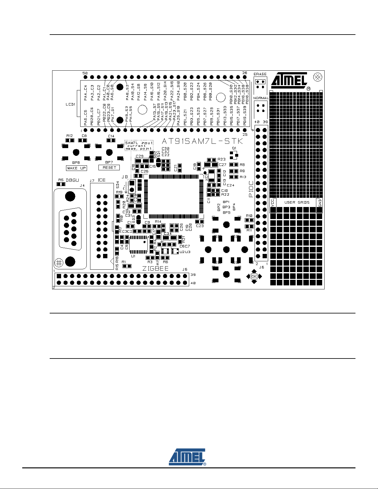
Setting Up the AT91SAM7L-STK Rev. A Board
2.3 Layout
Figure 2-1. AT91SAM7L-STK Rev. A Board Layout
2.4 Powering Up the Board
The AT91SAM7L-STK rev.A requires 3.0V (2.2V-3.6V) DC input. The power is supplied to the board via
2 AAA batteries or 3.0V VCC pads.
2.5 Getting Started
Please refer to the AT91SAM product pages on the Atmel web site, for the most up-to-date information
on getting started with the AT91SAM7L-STK rev.A.
2-2 AT91SAM7L-STK Rev. A Starter Kit User Guide
6409A–ATARM–30-Jun-08
Page 8
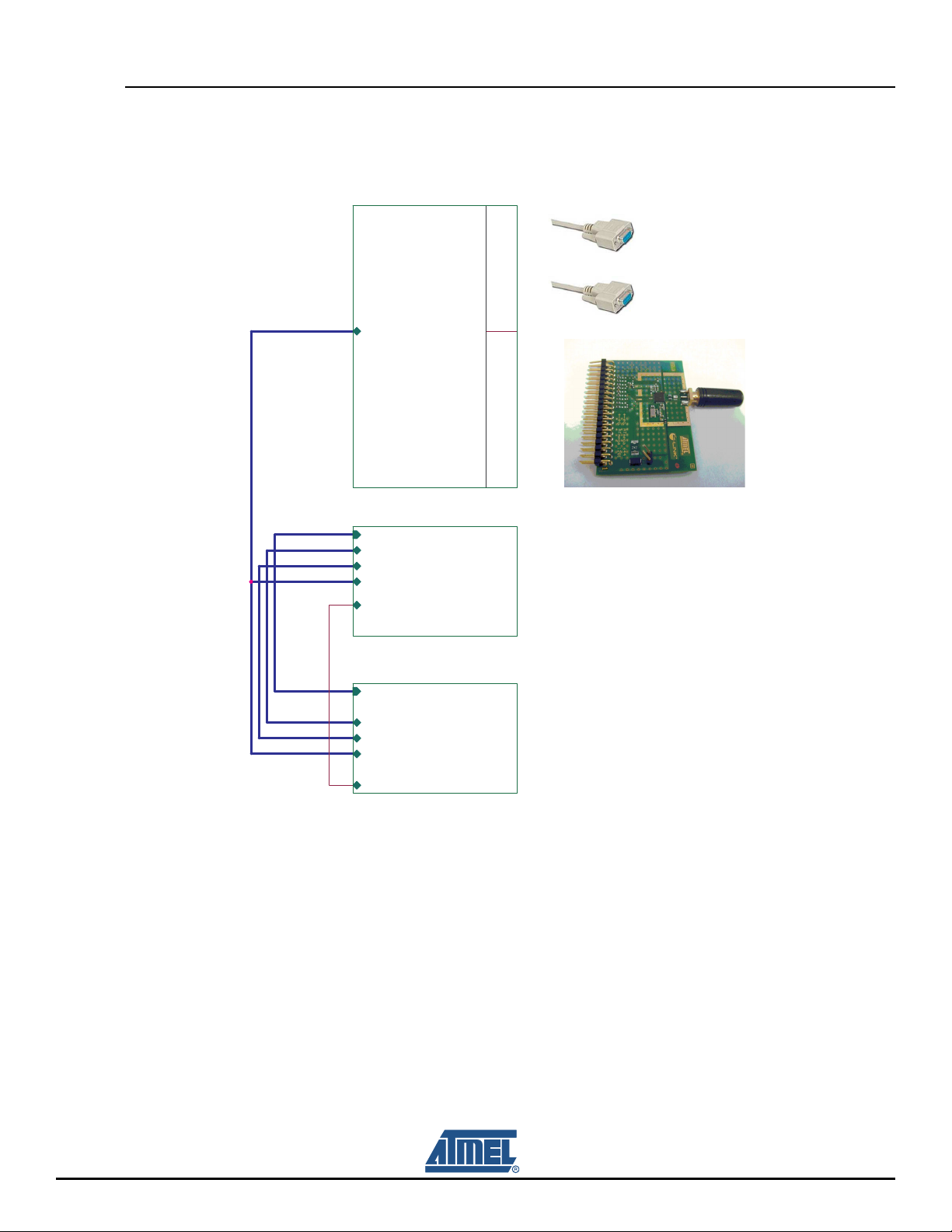
2.6 AT91SAM7L-STK Rev. A Block Diagram
Figure 2-2. AT91SAM7L-STK Block Diagram
Setting Up the AT91SAM7L-STK Rev. A Board
PC[0..29]
AD[0..3]
PA[0..25]
PB[0..23]
PC[0..29]
Interfaces
PC[0..29]
Interfaces
Processor
AD[0..3]
PA[0..25]
PB[0..23]
PC[0..29]
ERASE
Processor
SHEET 2
'%*8
56=,*%((
SHEET 4
AD[0..3]
PA[0..25]
PB[0..23]
PC[0..29]
LCD, KBD
AD[0..3]
PA[0..25]
PB[0..23]
PC[0..29]
ERASE
LCD, KBD
SHEET 3
AT91SAM7L-STK Rev. A Starter Kit User Guide 2-3
6409A–ATARM–30-Jun-08
Page 9

3.1 AT91SAM7L64/128 Microcontroller
• Incorporates the ARM7TDMI
– High-performance 32-bit RISC Architecture
– High-density 16-bit Instruction Set
– Leader in MIPS/Watt
– EmbeddedICE
™
In-circuit Emulation, Debug Communication Channel Support
• Internal High-speed Flash
– 128 Kbytes (AT91SAM7L128), Organized in 512 Pages of 256 Bytes Single Plane
– 64 Kbytes (AT91SAM7L64), Organized In 256 Pages of 256 Bytes Single Plane
– Single Cycle Access at Up to 15 MHz in Worst Case Conditions
– 128-bit Read Access
– Page Programming Time: 4.6 ms, Including Page Auto Erase, Full Erase Time: 10 ms
– 10,000 Write Cycles, 10-year Data Retention Capability, Sector Lock Capabilities, Flash Security Bit
– Fast Flash Programming Interface for High Volume Production
• Enhanced Embedded Flash Controller (EEFC)
– Interface of the Flash Block with the 32-bit Internal Bus
– Increases Performance in ARM and Thumb Mode with 128-bit Wide Memory Interface
• Internal High-speed SRAM, Single-cycle Access at Maximum Speed
– 6 kbytes
• 2 Kbytes Directly on Main Supply that Can Be Used as Backup SRAM
• 4 Kbytes in the Core
• Memory Controller (MC)
– Enhanced Embedded Flash Controller, Abort Status and Misalignment Detection
• Reset Controller (RSTC)
– Based on Brownout Reset and Low-power Factory-calibrated Brownout Detector
– Provides External Reset Signal Shaping and Reset Source Status
• Clock Generator (CKGR)
– Low-power 32 kHz RC Oscillator, 32 kHz On-chip Oscillator, 2 MHz Fast RC Oscillator and one PLL
• Supply Controller (SUPC)
– Minimizes Device Power Consumption
– Manages the Different Supplies On Chip
– Supports Multiple Wake-up Sources
• Power Management Controller (PMC)
– Software Power Optimization Capabilities, Including Slow Clock Mode (Down to 500 Hz) and Idle Mode
– Three Programmable External Clock Signals
– Handles Fast Start Up
• Advanced Interrupt Controller (AIC)
– Individually Maskable, Eight-level Priority, Vectored Interrupt Sources
– Two External Interrupt Sources and One Fast Interrupt Source, Spurious Interrupt Protected
®
ARM® Thumb® Processor
Section 3
Board Description
AT91SAM7L-STK Rev. A Starter Kit User Guide 3-1
6409A–ATARM–30-Jun-08
Page 10

Board Description
• Debug Unit (DBGU)
– Two-wire UART and Support for Debug Communication Channel interrupt, Programmable ICE Access
Prevention
• Periodic Interval Timer (PIT)
– 20-bit Programmable Counter plus 12-bit Interval Counter
• Windowed Watchdog (WDT)
– 12-bit Key-protected Programmable Counter
– Provides Reset or Interrupt Signals to the System
– Counter may be Stopped While the Processor is in Debug State or in Idle Mode
• Real-time Clock (RTC)
– Two Hundred Year Calendar with Alarm
– Runs Off the Internal RC or Crystal Oscillator
• Three Parallel Input/Output Controllers (PIOA, PIOB, PIOC)
– Eighty Programmable I/O Lines Multiplexed with up to Two Peripheral I/Os
– Input Change Interrupt Capability on Each I/O Line
– Individually Programmable Open-drain, Pull-up resistor and Synchronous Output
• Eleven Peripheral DMA Controller (PDC) Channels
• One Segmented LCD Controller
– Display Capacity of Forty Segments and Ten Common Terminals
– Software Selectable LCD Output Voltage (Contrast)
• Two Universal Synchronous/Asynchronous Receiver Transmitters (USART)
®
– Individual Baud Rate Generator, IrDA
– Support for ISO7816 T0/T1 Smart Card, Hardware Handshaking, RS485 Support
– Manchester Encoder/Decoder
– Full Modem Line Support on USART1
Infrared Modulation/Demodulation
• One Master/Slave Serial Peripheral Interface (SPI)
– 8- to 16-bit Programmable Data Length, Four External Peripheral Chip Selects
• One Three-channel 16-bit Timer/Counter (TC)
– Three External Clock Inputs, Two Multi-purpose I/O Pins per Channel
– Double PWM Generation, Capture/Waveform Mode, Up/Down Capability
• One Four-channel 16-bit PWM Controller (PWMC)
• One Two-wire Interface (TWI)
– Master, Multi-Master and Slave Mode Support, All Atmel® Two-wire EEPROMs and I2C compatible
Devices Supported
– General Call Supported in Slave Mode
• One 4-channel 10-bit Analog-to-Digital Converter, Four Channels Multiplexed with Digital I/Os
• SAM-BA
• IEEE
®
Boot Assistant
– Default Boot Program
– Interface with SAM-BA Graphic User Interface
– In Application Programming Function (IAP)
®
1149.1 JTAG Boundary Scan on All Digital Pins
• I/Os, including Four High-current Drive I/O lines, Up to 4 mA Each
• Power Supplies
– Embedded 1.8V Regulator, Drawing up to 60 mA for the Core with Programmable Output Voltage
– Single Supply 1.8V - 3.6V
– Zero-power Power-on Reset and Brownout Detector, Fully Programmable
• Fully Static Operation: Up to 36 MHz at 85°C
• Available in a 128-lead LQFP Green and a 144-ball LFBGA Green Package
3-2 AT91SAM7L-STK Rev. A Starter Kit User Guide
6409A–ATARM–30-Jun-08
Page 11

3.2 AT91SAM7L64/128 Block Diagram
Figure 3-1. AT91SAM7L64/128 Block Diagram
Board Description
TDO
TMS
TCK
JTAGSEL
TST
IRQ0-IRQ1
PCK0-PCK2
CLKIN
PLLRC
XOUT
VDDIO1
VDDIO1
NRST
RSTB
FWUP
TDI
FIQ
XIN
System Controller
PIO
PLL
OSC
32k RCOSC
BOD
POR
VDDIO1
JTAG
SCAN
2 MHz RCOSC
AIC
PMC
Supply
Controller
RTC
ICE
ARM7TDMI
Processor
Memory Controller
Embedded
Flash
Controller
Abort
Status
Peripheral Bridge
Peripheral Data
Controller
11 Channels
APB
Address
Decoder
Misalignment
Detection
Charge
Pump
LCD
Voltage
Regulator
1.8 V
Voltage
Regulator
SRAM
2 Kbytes( Back-up)
4 Kbytes (Core)
Flash
64/128 Kbytes
ROM (12 Kbytes)
Fast Flash
Programming
Interface
SAM-BA
CAPP1
CAPM1
CAPP2
CAPM2
VDDINLCD
VDD3V6
VDDLCD
VDDIO2
VDDIO1
GND
VDDOUT
VDDCORE
VDDIO2
VDDCORE
ERASE
PGMRDY
PGMNVALID
PGMNOE
PGMCK
PGMM0-PGMM3
PGMD0-PGMD15
PGMNCMD
PGMEN0-PGMEN2
DRXD
DTXD
SEG00-SEG39
COM0-COM9
RXD0
TXD0
SCK0
RTS0
CTS0
RXD1
TXD1
SCK1
RTS1
CTS1
DCD1
DSR1
DTR1
RI1
PIO
PIO
PIT
WDT
PDC
DBGU
PDC
PIOA (26 IOs)
PIOB (24 IOs)
PIOC (30 IOs)
LCD Controller
USART0
USART1
PDC
PDC
PDC
PDC
Timer Counter
PDC
PDC
PDC
PDC
PDC
PWMC
TC0
TC1
TC2
TWI
SPI
ADC
PIO
PWM0
PWM1
PWM2
PWM3
TCLK0
TCLK1
TCLK2
TIOA0
TIOB0
TIOA1
TIOB1
TIOA2
TIOB2
TWD
TWCK
NPCS0
NPCS1
NPCS2
NPCS3
MISO
MOSI
SPCK
ADTRG
AD0
AD1
AD2
AD3
ADVREF
AT91SAM7L-STK Rev. A Starter Kit User Guide 3-3
6409A–ATARM–30-Jun-08
Page 12

Board Description
3.3 Memory
6 Kbytes of Internal single-cycle access High-speed SRAM
64/128 Kbytes of Internal single-cycle access High-speed Flash
3.4 Clock Circuitry
32.768 KHz standard crystal for the oscillator
3.5 Reset Circuitry
Internal reset controller with a bi-directional reset pin
External reset push button
3.6 Shut Down controller
Programmable shutdown and Wake-Up
Wake-up push button.
3.7 Power Supply Circuitry
For dynamic power consumption, the AT91SAM7L64/128 consumes a maximum of 30 mA on VCC at
full speed 36MHz
On board 2 AAA batteries or 3V DC input power pad directly supplied to VCC
3.8 User Interface
Five user- input push buttons, four direction buttons and one ok button
3.9 Debug Interface
20-pin JTAG/ICE interface connector
One Serial interface (DBGU COM Port) via RS-232 DB9 male socket
3.10 Expansion Slot
One ZIGBEE expansion connector for Atmel AT86RF230 adaptor
All PIOC signals of the AT91SAM7L64/128 are routed to peripheral extension connector (J6). This
allows the developer to add external hardware components or boards.
3-4 AT91SAM7L-STK Rev. A Starter Kit User Guide
6409A–ATARM–30-Jun-08
Page 13

Board Description
3.11 PIO Usage
Table 3-1. PIO Controller A
I/O Line Peripheral A Peripheral B Peripheral Usage Powered by
PA0 Segment LCD PANEL COM0 VDDIO2
PA1 Segment LCD PANEL COM1 VDDIO2
PA2 Segment LCD PANEL COM2 VDDIO2
PA3 Segment LCD PANEL COM3 VDDIO2
PA4 Segment LCD PANEL COM4 VDDIO2
PA5 Segment LCD PANEL COM5 VDDIO2
PA6 Segment LCD PANEL SEG0 VDDIO2
PA7 Segment LCD PANEL SEG1 VDDIO2
PA8 Segment LCD PANEL SEG2 VDDIO2
PA9 Segment LCD PANEL SEG3 VDDIO2
PA10 Segment LCD PANEL SEG4 VDDIO2
PA11 Segment LCD PANEL SEG5 VDDIO2
PA12 Segment LCD PANEL SEG6 VDDIO2
PA13 Segment LCD PANEL SEG7 VDDIO2
PA14 Segment LCD PANEL SEG8 VDDIO2
PA15 Segment LCD PANEL SEG9 VDDIO2
PA16 Segment LCD PANEL SEG10 VDDIO2
PA17 Segment LCD PANEL SEG11 VDDIO2
PA18 Segment LCD PANEL SEG12 VDDIO2
PA19 Segment LCD PANEL SEG13 VDDIO2
PA20 Segment LCD PANEL SEG14 VDDIO2
PA21 Segment LCD PANEL SEG15 VDDIO2
PA22 Segment LCD PANEL SEG16 VDDIO2
PA23 Segment LCD PANEL SEG17 VDDIO2
PA24 Segment LCD PANEL SEG18 VDDIO2
PA25 Segment LCD PANEL SEG19 VDDIO2
AT91SAM7L-STK Rev. A Starter Kit User Guide 3-5
6409A–ATARM–30-Jun-08
Page 14

Board Description
Table 3-2. PIO Controller B
I/O Line Peripheral A Peripheral B Peripheral Usage Powered by
PB0 Segment LCD PANEL SEG20 VDDIO2
PB1 Segment LCD PANEL SEG21 VDDIO2
PB2 Segment LCD PANEL SEG22 VDDIO2
PB3 Segment LCD PANEL SEG23 VDDIO2
PB4 Segment LCD PANEL SEG24 VDDIO2
PB5 Segment LCD PANEL SEG25 VDDIO2
PB6 Segment LCD PANEL SEG26 VDDIO2
PB7 Segment LCD PANEL SEG27 VDDIO2
PB8 Segment LCD PANEL SEG28 VDDIO2
PB9 Segment LCD PANEL SEG29 VDDIO2
PB10 Segment LCD PANEL SEG30 VDDIO2
PB11 Segment LCD PANEL SEG31 VDDIO2
PB12 NPCS3 Segment LCD PANEL SEG32 VDDIO2
PB13 NPCS2 Segment LCD PANEL SEG33 VDDIO2
PB14 NPCS1 Segment LCD PANEL SEG34 VDDIO2
PB15 RTS1 Segment LCD PANEL SEG35 VDDIO2
PB16 RTS0 Segment LCD PANEL SEG36 VDDIO2
PB17 DTR1 Segment LCD PANEL SEG37 VDDIO2
PB18 PWM0 Segment LCD PANEL SEG38 VDDIO2
PB19 PWM1 Segment LCD PANEL SEG39 VDDIO2
PB20 PWM2 Segment LCD PANEL COM6 VDDIO2
PB21 PWM3 Segment LCD PANEL COM7 VDDIO2
PB22 NPCS1 PCK1 Segment LCD PANEL COM8 VDDIO2
PB23 PCK0 NPCS3 Segment LCD PANEL COM9 VDDIO2
3-6 AT91SAM7L-STK Rev. A Starter Kit User Guide
6409A–ATARM–30-Jun-08
Page 15

Board Description
Table 3-3. PIO Controller C
I/O Line Peripheral A Peripheral B Peripheral Usage Powered by
PC0 CTS1 PWM2 User’s Input Buttons OK VDDIO1
PC1 DCD1 TIOA2 User’s Input Buttons UP VDDIO1
PC2 DTR1 TIOB2 User’s Input Buttons RIGHT VDDIO1
PC3 DSR1 TCLK1 User’s Input Buttons DOWN VDDIO1
PC4 RI1 TCLK2 User’s Input Buttons LEFT VDDIO1
PC5 IRQ1 NPCS2 ZIGBEE IRQ1 VDDIO1
PC6 NPCS1 PCK2 ZIGBEE NPCS1 VDDIO1
PC7 PWM0 TIOA0 MAX3318E FORCEOFF VDDIO1
PC8 PWM1 TIOB0 ZIGBEE RSIN VDDIO1
PC9 PWM2 SCK0 ZIGBEE SLP_IR VDDIO1
PC10 TWD NPCS3 VDDIO1
PC11 TWCK TCLK0 VDDIO1
PC12 RXD0 NPCS3 MAX3318E FORCEON VDDIO1
PC13 TXD0 PCK0 MAX3318E INVALID VDDIO1
PC14 RTS0 ADTRG MAX3318E READY VDDIO1
PC15 CTS0 PWM3 VCC/VBAT MONITOR ENABLE VDDIO1
PC16 DRXD NPCS1 MAX3318E DRXD VDDIO1
PC17 DTXD NPCS2 MAX3318E DTXD VDDIO1
PC18 NPCS0 PWM0 VDDIO1
PC19 MISO PWM1 ZIGBEE MISO VDDIO1
PC20 MOSI PWM2 ZIGBEE MOSI VDDIO1
PC21 SPCK PWM3 ZIGBEE SPCK VDDIO1
PC22 NPCS3 TIOA1 VDDIO1
PC23 PCK0 TIOB1 VDDIO1
PC24 RXD1 PCK1 VDDIO1
PC25 TXD1 PCK2 VDDIO1
PC26 RTS0 FIQ VDDIO1
PC27 NPCS2 IRQ0 VDDIO1
PC28 SCK1 PWM0 VDDIO1
PC29 RTS1 PWM1 VDDIO1
AT91SAM7L-STK Rev. A Starter Kit User Guide 3-7
6409A–ATARM–30-Jun-08
Page 16

4.1 Configuration Straps
Table 4-1 gives details of configuration straps on the AT91SAM7L-STK rev. A starter board and their
default settings.
Table 4-1.
Designation Default Setting Feature
J6 pins 39-40 Opened Closed for internal flash erase
J8 Closed VCC jumper
SD1 Opened Disables VDDIO2 to VDDLCD connection
SD2 2-3 Selects VCC or VDD3V6 to VDDLCD
SD3 Closed Enables VDDOUT applying to VDDCORE
SD4 2-3 Selects VDDINLCD input
R20 IN Enables the ICE NRST input
TP1 N.A RX
TP2 N.A TX
Section 4
Configuration
(1)
(2)
TP3 N.A CLKIN
TP4 N.A FWUP
TP5 N.A ADREF
TP6 N.A XOUT
TP7 N.A NRSTB
TP8 N.A VDDIO2
TP9 N.A VDD3V6
TP10 N.A VDDOUT
Notes: 1. This jumper is used to erase and reinitialize the internal flash content and some of the NVM bits.
2. This jumper is provided for power consumption measurement. By default, it is closed. To use this feature, the user has to open the strap and insert an ammeter.
AT91SAM7L-STK Rev. A Starter Kit User Guide 4-1
6409A–ATARM–30-Jun-08
Page 17

This section contains the following schematics:
Top Level
Interfaces
LCD, KBD
Processor
Section 5
Schematics
AT91SAM7L-STK Rev. A Starter Kit User Guide 5-1
6409A–ATARM–30-Jun-08
Page 18

5
4
3
2
1
Interfaces
SHEET 2
D D
PC[0..29]
PC[0..29]
C C
Interfaces
AD[0..3]
PA[0..25]
PB[0..23]
PC[0..29]
Processor
AD[0..3]
PA[0..25]
PB[0..23]
PC[0..29]
ERASE
Processor
SHEET 4
B B
AD[0..3]
PA[0..25]
PB[0..23]
PC[0..29]
LCD, KBD
AD[0..3]
PA[0..25]
PB[0..23]
PC[0..29]
ERASE
LCD, KBD
SHEET 3
A A
INIT EDIT
INIT EDIT
INIT EDIT
A
A
A
REV
REV
REV
SCALE
SCALE
AT91SAM7L-STK
AT91SAM7L-STK
AT91SAM7L-STK
Top level
Top level
Top level
This agreement is our property. Reproduction and publication without our written authorization shall expose offender to legal proceedings.
This agreement is our property. Reproduction and publication without our written authorization shall expose offender to legal proceedings.
This agreement is our property. Reproduction and publication without our written authorization shall expose offender to legal proceedings.
SCALE
1/1
1/1
1/1
DES.
DES.
DES.
17MAR08
17MAR08
17MAR08
DATE
DATE
DATE
XX-XXX-XXPP XXX
XX-XXX-XXPP XXX
XX-XXX-XXPP XXX
DATEMODIF.
VER.
DATEMODIF.
VER.
DATEMODIF.
VER.
REV. SHEET
REV. SHEET
REV. SHEET
1
1
1
A
A
A
4
4
4
Page 19

5
4
3
2
1
J1
J1
J2
C1+
C2+
INVALID
READY
FORCEON
D1IN
D2IN
R1OUT
R2OUT
1
1
PadJ2Pad
J3
1
1
PadJ3Pad
2
C2
100NFC2100NF
4
C1-
5
C3
100NFC3100NF
6
C2-
PC13
11
PC14 PC12
1
20
14
13
12
GND
15
10
R1
100KR1100K
R2
100KR2100K
R4
R4
NOT POPULATED
NOT POPULATED
GND
DTXD
DRXD
R3
100KR3100K
PC7
PC17
PC16
AAA
AAA
AAA
AAA
GND
D D
VCC
VCC VCC
U1
U1
19
GND
VCC
18
GND
3
V+
7
V-
FORCEOFF
17
D1OUT
8
D2OUT
16
R1IN
9
R2IN
C1
100NFC1100NF
SERIAL DEBUG PORT
GND
C5
100NFC5100NF
TX
RX
C4
J4
C C
J4
10
11
1
6
2
7
3
8
4
9
5
D09P24A4GX00
D09P24A4GX00
TP1
TP1
TESTPOINT
TESTPOINT
TP2
TP2
TESTPOINT
TESTPOINT
R5 0RR5 0R
100NFC4100NF
PC0
PC1
PC2
PC3
PC4
PC5
PC6
PC7
PC8
PC9
PC10
PC11
PC12
PC13
PC14
PC15
PC16
PC17
PC18
PC19
PC20
PC21
PC22
PC23
PC24
PC25
PC26
PC27
PC28
PC29
PC[0..29]
MAX3318E
GND
B B
Note: Pin 1 on Zigbee board RZ502 matches pin 2 on this connector
VCC VCC
SLP_TR
PC9
MOSI
PC20
PC6
IRQ1
PC5
J5J5
1 2
3 4
5 6
7 8
9 10
11 12
13
15
17
19
21 22
23 24
25 26
27 28
29 30
31 32
33 34
35 36
37 38
39 40
14
16
18
20
MAX3318E
GND
ZIGBEE INTERFACE
VCC
RSTN
PC8
MISO
SPCKNPSC1
PC21
R7
10KR710K
VCC
U2
U2
3
D
1
CP
6
C
NC7SZ175P6X
NC7SZ175P6X
R6 0RR6 0R
VCC
U3
5
VCC
Q
GND
VCC VCC
VCC
4
2
GND
C6
C6
NOT POPULATED
NOT POPULATED
GND GND
U3
2 4
3 5
1
GND
NC7SZ125P5X
NC7SZ125P5X
C7
C7
NOT POPULATED
NOT POPULATED
Only for AT86RF230Rev.A connexion
not required for Rev.B on
PC19
A A
GND
INIT EDIT
INIT EDIT
INIT EDIT
A
A
A
REV
REV
REV
SCALE
SCALE
AT91SAM7L-STK
AT91SAM7L-STK
AT91SAM7L-STK
Interfaces
Interfaces
Interfaces
This agreement is our property. Reproduction and publication without our written authorization shall expose offender to legal proceedings.
This agreement is our property. Reproduction and publication without our written authorization shall expose offender to legal proceedings.
This agreement is our property. Reproduction and publication without our written authorization shall expose offender to legal proceedings.
SCALE
1/1
1/1
1/1
DES.
DES.
DES.
17MAR08
17MAR08
17MAR08
DATE
DATE
DATE
XX-XXX-XXPP XXX
XX-XXX-XXPP XXX
XX-XXX-XXPP XXX
DATEMODIF.
VER.
DATEMODIF.
VER.
DATEMODIF.
VER.
REV. SHEET
REV. SHEET
REV. SHEET
2
2
2
A
A
A
4
4
4
Page 20

5
PC[0..29]
PB[0..23]
PA[0..25]
D D
PA0 COM0
PA1 COM1
PA2 COM2 PB2 SEG22
PA3 COM3
PA4 COM4
PA5 COM5
PA6 SEG0
PA7 SEG1
PA8 SEG2
PA9 SEG3
PA10 SEG4
PA11 SEG5
PA12 SEG6
PA13 SEG7
PA14 SEG8
PA15 SEG9
PA16 SEG10
PA17 SEG11
PA18 SEG12
PA19 SEG13
PA20 SEG14
PA21 SEG15
C C
AD[0..3]
PA22 SEG16
PA23 SEG17
PA24 SEG18
PA25 SEG19
4
AD3
AD2
AD1
AD0
PB0 SEG20
PB1 SEG21
PB3 SEG23
PB4 SEG24
PB5 SEG25
PB6 SEG26
PB7 SEG27
PB8 SEG28
PB9 SEG29
PB10 SEG30
PB11 SEG31
PB12 SEG32
PB13 SEG33
PB14 SEG34
PB15 SEG35
PB16 SEG36
PB17 SEG37
PB18 SEG38
PB19 SEG39
PB20 COM6
PB21 COM7
PB22 COM8
PB23 COM9
NPCS3
NPCS2
NPCS1
RTS1
RTS0
DTR1
PWM0
PWM1
PWM2
PWM3
NPSC1/PCK1
PCK0/NPCS3
PC0
PC1
PC2
PC3
PC4
PC5
PC6
PC7
PC8
PC9
PC10
PC11
PC12
PC13
PC14
PC15
PC16
PC17
PC18
PC19
PC20
PC21
PC22
PC23
PC24
PC25
PC26
PC27
PC28
PC29
UP
RIGHT
DOWN
LEFT
3
BP2
BP2
3-1437565-0
3-1437565-0
GND GND GND
VCC/VBAT MONITOR
AD[0..3]
AD3
2
BP1
BP1
3-1437565-0
3-1437565-0
BP3
BP3
3-1437565-0
3-1437565-0
BP5
BP5
3-1437565-0
3-1437565-0
VCC
3 2
R8
10KR810K
Q1
FDV304PQ1FDV304P
1
PC15
BP4
BP4
3-1437565-0
3-1437565-0
PC1
PC0
PC2
PC4
PC3
1
UP
OK
RIGHT
LEFT
DOWNOK
VCC
R9
10KR910K
VCC VCC
COM4
COM3
COM2
COM1
COM0
SEG0
SEG2
SEG4
SEG6
SEG8
SEG10
SEG12
SEG14
SEG16
46
B B
COM550COM449COM348COM247COM1
COM61COM72COM83COM94COM105SEG26SEG47SEG68SEG89SEG1010SEG1211SEG1412SEG1613SEG1814SEG2015SEG2216SEG2417SEG2618SEG2819SEG3020SEG3221SEG3422SEG36
COM5
COM6
COM7
COM9
COM8
SEG145SEG344SEG543SEG742SEG9
SEG1
SEG3
41
SEG1140SEG1339SEG1538SEG1737SEG1936SEG2135SEG2334SEG2533SEG2732SEG2931SEG3130SEG3329SEG3528SEG3727SEG39
SEG5
SEG7
SEG9
SEG11
SEG13
SEG15
SEG17
SEG22
SEG24
SEG26
SEG28
SEG30
SEG32
SEG34
SEG18
SEG20
SEG23
SEG25
SEG27
SEG19
SEG21
SEG29
SEG36
SEG38SEG39
R10
R10
NOT POPULATED
26
LCD1
LCD1
LCD_GS08001AA
LCD_GS08001AA
SEG4025SEG38
24
23
SEG31
SEG33
SEG35
SEG37
NOT POPULATED
GND
PC1
PC3
PC5
PC7
PC9
PC11
PC13
PC15
PC17
PC19
PC21
PC23
PC25
PC27
AD1
AD3
VCC
GND
J6J6
1 2
3 4
5 6
7 8
9 10
11 12
13
15
17
19
21 22
23 24
25 26
27 28
29 30
31 32
33 34
35 36
37 38
39 40
JS1JS1
R11
R11
NOT POPULATED
NOT POPULATED
PC0
CTS1/PWM2_WKUP0DCD1/TIOA2_WKUP1
PC2
DTR1/TIOB2_WKUP2DSR1/TCLK1_WKUP3
PC4
RI1/TCLK2_WKUP4IRQ1/NPCS2_WKUP5
PC6
NPCS1/PCK2_WKUP6PWM0/TIOA0
PC8
PWM1/TIOB0PWM2/SCK0
PC10
TWD/NPCS3TWCK/TCLK0_WKUP7
PC12
PC14
PC16
PC18
PC20
PC22
PC24
PC26
PC28PC29
AD0
AD2
ERASE
RXD0/NPCS3_WKUP8TXD0/PCK0_WKUP9
RTS0/ADTRG_WKUP10CTS0/PWM3_WKUP11
DRXD/NPCS1/DTXD/MPCS2
NPCS0/PWM0MISO/PWM1
MOSI/PWM2SPCK/PWM3
MPCS3/TIOA1PCK0/TIOB1
RXD1/PCK1TXD1/PCK2
RTS0/FIQ_WKUP12NPCS2/IRQ0_WKUP13
SCK1/PWM0_WKUP14RTS1/PWM1_WKUP15
ERASE
GND
14
16
18
20
GND
A A
INIT EDIT
INIT EDIT
INIT EDIT
A
A
A
REV
REV
REV
SCALE
SCALE
AT91SAM7L-STK
AT91SAM7L-STK
AT91SAM7L-STK
LCD, KBD
LCD, KBD
LCD, KBD
This agreement is our property. Reproduction and publication without our written authorization shall expose offender to legal proceedings.
This agreement is our property. Reproduction and publication without our written authorization shall expose offender to legal proceedings.
This agreement is our property. Reproduction and publication without our written authorization shall expose offender to legal proceedings.
SCALE
1/1
1/1
1/1
DES.
DES.
DES.
17MAR08
17MAR08
17MAR08
DATE
DATE
DATE
XX-XXX-XXPP XXX
XX-XXX-XXPP XXX
XX-XXX-XXPP XXX
DATEMODIF.
VER.
DATEMODIF.
VER.
DATEMODIF.
VER.
REV. SHEET
REV. SHEET
REV. SHEET
3
3
3
A
A
A
4
4
4
Page 21

PB[0..23]
FORCE WAKE-UP
VCC
5
TP3
TP3
TESTPOINT
TESTPOINT
4
PC2
PC3
PC0
PC1
U4 AT91SAM7L128-AU
U4 AT91SAM7L128-AU
87
88
89
90
3
PC16
PC19
PC18
PC17
PC20
PC22
PC21
PC5
PC6
PC9
PC4
PC8
PC7
PC10
PC15
PC14
PC12
PC11
PC13
91
92
93
95
96
97
98
99
101
102
103
104
PC23
PC24
PC25
PC26
PC27
PC28
PC29
105
106
107
108
109
110
111
112
113
114
115
77
78
2
1
PC[0..29]
PA[0..25]
ERASE
VCC
PA0
PA1
PA2
PA3
PA4
PA5
PA6
PA7
PA8
PA9
PA10
PA11
PA12
PA13
PA14
PA15
PA16
PA17
PA18
PA19
PA20
PA21
PA22
PA23
PA24
PA25
AD3
AD2
AD1
AD0
R23
R23
NOT POPULATED
NOT POPULATED
TP7
TP7
TESTPOINT
TESTPOINT
ERASE
TP8
TP8
TESTPOINT
TESTPOINT
SAM7L Current measurement
AT91SAM7L-STK
AT91SAM7L-STK
AT91SAM7L-STK
Processor
Processor
Processor
This agreement is our property. Reproduction and publication without our written authorization shall expose offender to legal proceedings.
This agreement is our property. Reproduction and publication without our written authorization shall expose offender to legal proceedings.
This agreement is our property. Reproduction and publication without our written authorization shall expose offender to legal proceedings.
GND
GND
VDDOUT
R14
R14
180R
180R
C9
100NFC9100NF
A
A
A
REV
REV
REV
SCALE
SCALE
SCALE
TESTPOINT
TESTPOINT
VCC
INIT EDIT
INIT EDIT
INIT EDIT
1/1
1/1
1/1
TP5
TP5
C14
C14
10NF
10NF
DES.
DES.
DES.
RESET
17MAR08
17MAR08
17MAR08
DATE
DATE
DATE
AD[0..3]
GND
NRSTB
BP7
BP7
3-1437565-0
3-1437565-0
XX-XXX-XXPP XXX
XX-XXX-XXPP XXX
XX-XXX-XXPP XXX
DATEMODIF.
VER.
DATEMODIF.
VER.
DATEMODIF.
VER.
REV. SHEET
REV. SHEET
REV. SHEET
4
4
4
A
A
A
4
4
4
VCC
PB0
PB1
PB2
PB3
PB4
PB5
PB6
PB7
PB8
PB9
PB10
PB11
PB12
PB13
PB14
PB15
PB16
PB17
PB18
PB19
PB20
PB21
PB22
PB23
R21
R21
NOT POPULATED
NOT POPULATED
32.768 kHz
32.768 kHz
C13
C13
18PF
18PF
D D
R12
R12
100K
100K
R13
R13
100K
100K
FWKUP
BP6
GND
BP6
3-1437565-0
3-1437565-0
C8
C8
NOT POPULATED
NOT POPULATED
TP4
TP4
TESTPOINT
TESTPOINT
GND
ICE INTERFACE
VCC
VCC
R16
R16
R17
R15
C C
J7J7
12
34
56
78
910
1112
13
14
15
16
17
18
19
20
GND
R15
100K
100K
R20 0RR20 0R
JTAG_TDI
JTAG_TMS
JTAG_TCK
JTAG_TDO
JTAG_RST
100K
100K
C10
C10
C11
C11
22NF
22NF
2.2NF
2.2NF
R17
100K
100K
R18
R18
100K
100K
R22
R22
10K
10K
TP6
TP6
TESTPOINT
TESTPOINT
R19
R19
NOT POPULATED
NOT POPULATED
CM415-32.768KDZFB-F
CM415-32.768KDZFB-F
XC1
XC1
1 2
C12
C12
18PF
18PF
B B
GND
C30
C30
100NF
100NF
2
SD1
SD1
2
SOLDER DROP 2 pins open
SOLDER DROP 2 pins open
1
1
VCC
1 2
SOLDER DROP 3 pins
SOLDER DROP 3 pins
A A
SD2
SD2
41
42
43
44
45
46
47
48
49
50
51
52
53
54
57
58
59
60
61
63
64
65
66
67
125
118
116
82
81
117
79
83
121
122
128
127
123
3
PB0_SEG20
PB1_SEG21
PB2_SEG22
PB3_SEG23
PB4_SEG24
PB5_SEG25
PB6_SEG26
PB7_SEG27
PB8_SEG28
PB9_SEG29
PB10_SEG30
PB11_SEG31
PB12/NPCS3_SEG32
PB13/NPCS2_SEG33
PB14/NPCS1_SEG34
PB15/RTS1_SEG35
PB16/RTS0_SEG36
PB17/DTR1_SEG37
PB18/PWM0_SEG38
PB19/PWM1_SEG39
PB20/PWM2_COM6
PB21/PWM3_COM7
PB22/NPSC1/PCK1_COM8
PB23/PCK0/NPCS3_COM9
CLKIN
AT91SAM7L-LQFP128
FWUP
TDI
TMS
TCK
TDO
NRST
JTAGSEL
PLLRC
PLLRCGND
XOUT
XIN/PGMCK
GNDPLL
C29
C29
10µF
10µF
6V3
6V3
TP9
TP9
TESTPOINT
TESTPOINT
AT91SAM7L-LQFP128
VDDLCD33VDD3V6
34
C15
C15
220NF
220NF
C34
C34
10µF
10µF
6V3
6V3
TP10
TP10
TESTPOINT
TESTPOINT
PC4/RI1/TCLK2_WKUP4
PC2/DTR1/TIOB2_WKUP2
PC0/CTS1/PWM2_WKUP0
PC1/DCD1/TIOA2_WKUP1
PC3/DSR1/TCLK1_WKUP3
CAPM235CAPP236CAPM137CAPP1
38
C16
C16
220NF
220NF
VDDOUT
SOLDER DROP 2 pins closed
SOLDER DROP 2 pins closed
PA0_COM0
PA1_COM1
PA2_COM2
PA3_COM3
VDDIO215VDDIO232VDDIO2
55
C32 100NFC32 100NF
C21 100NFC21 100NF
C27 6V310µFC27 6V310µF
SOLDER DROP 3 pins
SOLDER DROP 3 pins
3
SD4
SD4
1 2
GND
PA4_COM4
PA5_COM5
PA10_SEG4
PA11_SEG5
PA12_SEG6
PA13_SEG7
PA14_SEG8
PA15_SEG9
PA16_SEG10
PA17_SEG11
PA18_SEG12
PA19_SEG13
PA20_SEG14
PA21_SEG15
PA22_SEG16
PA23_SEG17
PA24_SEG18
PA25_SEG19
C28 100NFC28 100NF
PC9/PWM2/SCK0
PC7/PWM0/TIOA094PC8/PWM1/TIOB0
PC10/TWD/NPCS3
PC5/IRQ1/NPCS2_WKUP5
PC6/NPCS1/PCK2_WKUP6
PC11/TWCK/TCLK0_WKUP7
VDDCORE62VDDCORE
VDDCORE
VDDCORE28VDDCORE
VDDOUT
74
VDDCORE
2
84
100
124
C23 100NFC23 100NF
C19 100NFC19 100NF
C22 100NFC22 100NF
C17 2.2µFC17 2.2µF
C31 100NFC31 100NF
C18 100NFC18 100NF
SD3
SD3
2
112
PC17/DTXD/MPCS2
PC16/DRXD/NPCS1
PC18/NPCS0/PWM0
PC13/TXD0/PCK0_WKUP9
PC12/RXD0/NPCS3_WKUP8
PC15/CTS0/PWM3_WKUP11
PC14/RTS0/ADTRG_WKUP10
GND14GND76GND
40
68
C24 100NFC24 100NF
PC25/TXD1/PCK2
PC24/RXD1/PCK1
PC23/PCK0/TIOB1
PC19/MISO/PWM1
PC20/MOSI/PWM2
PC21/SPCK/PWM3
PC22/MPCS3/TIOA1
PC26/RTS0/FIQ_WKUP12
PC29/RTS1/PWM1_WKUP15
PC28/SCK1/PWM0_WKUP14
PC27/NPCS2/IRQ0_WKUP13
GND
GND86GND56GND
120
GND
VDDIO185VDDIO1
VDDINLCD
VDDIO1
39
75
119
C26 100NFC26 100NF
C20 100NFC20 100NF
C25 100NFC25 100NF
PA6_SEG0
PA7_SEG1
PA8_SEG2
PA9_SEG3
ADVREF
AD3
AD2
AD1
AD0
TST
NRSTB
ERASE
80
C33
C33
10µF
10µF
6V3
6V3
J8J8
3
4
5
6
7
8
9
10
11
12
13
16
17
18
19
20
21
22
23
24
25
26
27
29
30
31
69
70
71
72
73
1
126
R24
R24
10R
10R
JS2JS2
Page 22

6.1 Q1 Footprint Incorrect
Transistor Q1 is incorrectly connected. The schematic is right but the PCB connections of pins S and D
are swapped => the protection diode is polarized forward (permanent current flow across the bridge) and
the MOS is not operating properly (non accurate battery level measurement).
Problem Fix/Workaround
Remove Q1 in order to avoid the parasitic 150 µA battery drain. If battery measurement is really mandatory for some applications, Q1 has to be removed and soldered bottom up, taking care to apply the
correct polarity. Additionally, a 100 KΩ pull-up resistor is needed across gate and source.
6.2 MAX3318 Control Pull-ups
The default configuration of the MAX3318 is ON. This leads to extra power consumption discharging the
batteries when the AT91SAM7L128 enters OFF mode (or does not even drive PC7 and PC12 to put the
MAX3318 in OFF mode).
Section 6
Errata
Problem Fix/Workaround
Remove R1, R2 and R3 and add a 10M Ω pull-down resistor on PC7. This allows to Force OFF the
MAX3318 when the AT91SAM7L128 enters OFF mode and to turn it on when the AT91SAM7L128
wakes up. The user can save power consumption by driving PC7 connected to the FORCEOFF pin of
the MAX3318.
AT91SAM7L-STK Rev. A Starter Kit User Guide 6-1
6409A–ATARM–30-Jun-08
Page 23

Doc Rev Comments
6409A First issue.
Section 7
Revision History
Change
Request Ref.
AT91SAM7L-STK Rev. A Starter Kit User Guide 7-1
6409A–ATARM–30-Jun-08
Page 24

Headquarters International
Atmel Corporation
2325 Orchard Parkway
San Jose, CA 95131
USA
Tel: 1(408) 441-0311
Fax: 1(408) 487-2600
Atmel Asia
Room 1219
Chinachem Golden Plaza
77 Mody Road Tsimshatsui
East Kowloon
Hong Kong
Tel: (852) 2721-9778
Fax: (852) 2722-1369
Product Contact
Web Site
www.atmel.com
www.atmel.com/AT91SAM
Literature Requests
www.atmel.com/literature
Atmel Europe
Le Krebs
8, Rue Jean-Pierre Timbaud
BP 309
78054 Saint-Quentin-enYvelines Cedex
France
Tel: (33) 1-30-60-70-00
Fax: (33) 1-30-60-71-11
Technical Support
AT91SAM Support
Atmel techincal support
Atmel Japan
9F, Tonetsu Shinkawa Bldg.
1-24-8 Shinkawa
Chuo-ku, Tokyo 104-0033
Japan
Tel: (81) 3-3523-3551
Fax: (81) 3-3523-7581
Sales Contacts
www.atmel.com/contacts/
Disclaimer: The information in this document is provided in connection with Atmel products. No license, express or implied, by estoppel or otherwise, to any
intellectual property right is granted by this document or in connection with the sale of Atmel products. EXCEPT AS SET FORTH IN ATMEL’S TERMS AND CONDI-
TIONS OF SALE LOCATED ON ATMEL’S WEB SITE, ATMEL ASSUMES NO LIABILITY WHATSOEVER AND DISCLAIMS ANY EXPRESS, IMPLIED OR STATUTORY
WARRANTY RELATING TO ITS PRODUCTS INCLUDING, BUT NOT LIMITED TO, THE IMPLIED WARRANTY OF MERCHANTABILITY, FITNESS FOR A PARTICULAR
PURPOSE, OR NON-INFRINGEMENT. IN NO EVENT SHALL ATMEL BE LIABLE FOR ANY DIRECT, INDIRECT, CONSEQUENTIAL, PUNITIVE, SPECIAL OR INCIDENTAL DAMAGES (INCLUDING, WITHOUT LIMITATION, DAMAGES FOR LOSS OF PROFITS, BUSINESS INTERRUPTION, OR LOSS OF INFORMATION) ARISING OUT OF
THE USE OR INABILITY TO USE THIS DOCUMENT, EVEN IF ATMEL HAS BEEN ADVISED OF THE POSSIBILITY OF SUCH DAMAGES. Atmel makes no
representations or warranties with respect to the accuracy or completeness of the contents of this document and reserves the right to make changes to specifications
and product descriptions at any time without notice. Atmel does not make any commitment to update the information contained herein. Unless specifically provided
otherwise, Atmel products are not suitable for, and shall not be used in, automotive applications. Atmel’s products are not intended, authorized, or warranted for use
as components in applications intended to support or sustain life.
© 2008 Atmel Corporation. All rights reserved. Atmel®, logo and combinations thereof, SAM-BA® and others are registered trademarks or trade-
marks of Atmel Corporation or its subsidiaries. ARM
®
, ARMPowered® logo and others are registered trademarks or trademarks of ARM Ltd.
Other terms and product names may be trademarks of others.
6409A–ATARM–30-Jun-08
 Loading...