

Page 1

BDTIC www.bdtic.com/ATMEL
Features
• Incorporates the ARM7TDMI
– High-performance 32-bit RISC Architecture
– High-density 16-bit Instruction Set
– Leader in MIPS/Watt
• EmbeddedICE
• 256 Kbytes of Internal High-speed Flash, Organized in 1024 Pages of 256 Bytes
– Single Cycle Access at Up to 30 MHz in Worst Case Conditions
– Prefetch Buffer Optimizing Thumb Instruction Execution at Maximum Speed
– Page Programming Time: 6 ms, Including Page Auto-erase, Full Erase Time: 15 ms
– 10,000 Write Cycles, 10-year Data Retention Capability, Sector Lock Capabilities
• 32K Bytes of Internal High-speed SRAM, Single-cycle Access at Maximum Speed
• Memory Controller (MC)
– Embedded Flash Controller, Abort Status and Misalignment Detection
– Memory Protection Unit
• Reset Controller (RSTC)
– Based on Three Power-on Reset Cells
– Provides External Reset Signal Shaping and Reset Sources Status
• Clock Generator (CKGR)
– Low-power RC Oscillator, 3 to 20 MHz On-chip Oscillator and One PLL
• Power Management Controller (PMC)
– Power Optimization Capabilities, including Slow Clock Mode (Down to 500 Hz), Idle
Mode, Standby Mode and Backup Mode
– Four Programmable External Clock Signals
• Advanced Interrupt Controller (AIC)
– Individually Maskable, Eight-level Priority, Vectored Interrupt Sources
– Four External Interrupt Sources and One Fast Interrupt Source, Spurious Interrupt
Protected
• Debug Unit (DBGU)
– 2-wire UART and Support for Debug Communication Channel interrupt
• Periodic Interval Timer (PIT)
– 20-bit Programmable Counter plus 12-bit Interval Counter
• Windowed Watchdog (WDT)
– 12-bit key-protected Programmable Counter
– Provides Reset or Interrupt Signal to the System
– Counter May Be Stopped While the Processor is in Debug Mode or in Idle State
• Real-time Timer (RTT)
– 32-bit Free-running Counter with Alarm
– Runs Off the Internal RC Oscillator
• Two Parallel Input/Output Controllers (PIO)
– Sixty-two Programmable I/O Lines Multiplexed with up to Two Peripheral I/Os
– Input Change Interrupt Capability on Each I/O Line
– Individually Programmable Open-drain, Pull-up resistor and Synchronous Output
• Shutdown Controller (SHDWC)
– Programmable Shutdown Pin and Wake-up Circuitry
• Two 32-bit Battery Backup Registers for a Total of 8 Bytes
• One 8-channel 20-bit PWM Controller (PWMC)
• One USB 2.0 Full Speed (12 Mbits per Second) Device Port
– On-chip Transceiver, 2376-byte Configurable Integrated FIFOs
™
In-circuit Emulation, Debug Communication Channel Support
®
ARM® Thumb® Processor
AT91 ARM
Thumb-based
Microcontrollers
AT91SAM7A3
Preliminary
6042E–ATARM–14-Dec-06
Page 2

• Nineteen Peripheral DMA Controller (PDC) Channels
• Two CAN 2.0B Active Controllers, Supporting 11-bit Standard and 29-bit Extended Identifiers
– 16 Fully Programmable Message Object Mailboxes, 16-bit Time Stamp Counter
• Two 8-channel 10-bit Analog-to-Digital Converter
• Three Universal Synchronous/Asynchronous Receiver Transmitters (USART)
®
– Individual Baud Rate Generator, IrDA
– Support for ISO7816 T0/T1 Smart Card, Hardware Handshaking, RS485 Support
Infrared Modulation/Demodulation
• Two Master/Slave Serial Peripheral Interfaces (SPI)
– 8- to 16-bit Programmable Data Length, Four External Peripheral Chip Selects
• Three 3-channel 16-bit Timer/Counters (TC)
– Three External Clock Inputs, Two Multi-purpose I/O Pins per Channel
– Double PWM Generation, Capture/Waveform Mode, Up/Down Capability
• Two Synchronous Serial Controllers (SSC)
– Independent Clock and Frame Sync Signals for Each Receiver and Transmitter
– I²S Analog Interface Support, Time Division Multiplex Support
– High-speed Continuous Data Stream Capabilities with 32-bit Data Transfer
• One Two-wire Interface (TWI)
– Master Mode Support Only, All Two-wire Atmel EEPROM’s Supported
• Multimedia Card Interface (MCI)
– Compliant with Multimedia Cards and SD Cards
– Automatic Protocol Control and Fast Automatic Data Transfers with PDC, MMC and SDCard Compliant
®
• IEEE
1149.1 JTAG Boundary Scan on All Digital Pins
• Required Power Supplies
– Embedded 1.8V Regulator, Drawing up to 130 mA for the Core and the External Components, Enables 3.3V Single Supply
Mode
– 3.3V VDD3V3 Regulator, I/O Lines and Flash Power Supply
– 1.8V VDD1V8 Output of the Voltage Regulator and Core Power Supply
– 3V to 3.6V VDDANA ADC Power Supply
– 3V to 3.6V VDDBU Backup Power Supply
• 5V-tolerant I/Os
• Fully Static Operation: Up to 60 MHz at 1.65V and 85°C Worst Case Conditions
• Available in a 100-lead LQFP Green Package
2
AT91SAM7A3 Preliminary
6042E–ATARM–14-Dec-06
Page 3

1. Description
AT91SAM7A3 Preliminary
The AT91SAM7A3 is a member of a series of 32-bit ARM7™ microcontrollers with an integrated CAN controller. It features a 256-Kbyte high-speed Flash and 32-Kbyte SRAM, a large
set of peripherals, including two 2.0B full CAN controllers, and a complete set of system functions minimizing the number of external components. The device is an ideal migration path for
8-bit microcontroller users looking for additional performance and extended memory.
The embedded Flash memory can be programmed in-system via the JTAG-ICE interface.
Built-in lock bits protect the firmware from accidental overwrite.
The AT91SAM7A3 integrates a complete set of features facilitating debug, including a JTAG
Embedded ICE interface, misalignment detector, interrupt driven debug communication channel for user configurable trace on a console, and JTAG boundary scan for board level debug
and test.
By combining a high-performance 32-bit RISC processor with a high-density 16-bit instruction
set, Flash and SRAM memory, a wide range of peripherals including CAN controllers, 10-bit
ADC, Timers and serial communication channels, on a monolithic chip, the AT91SAM7A3 is
ideal for many compute-intensive embedded control applications.
6042E–ATARM–14-Dec-06
3
Page 4
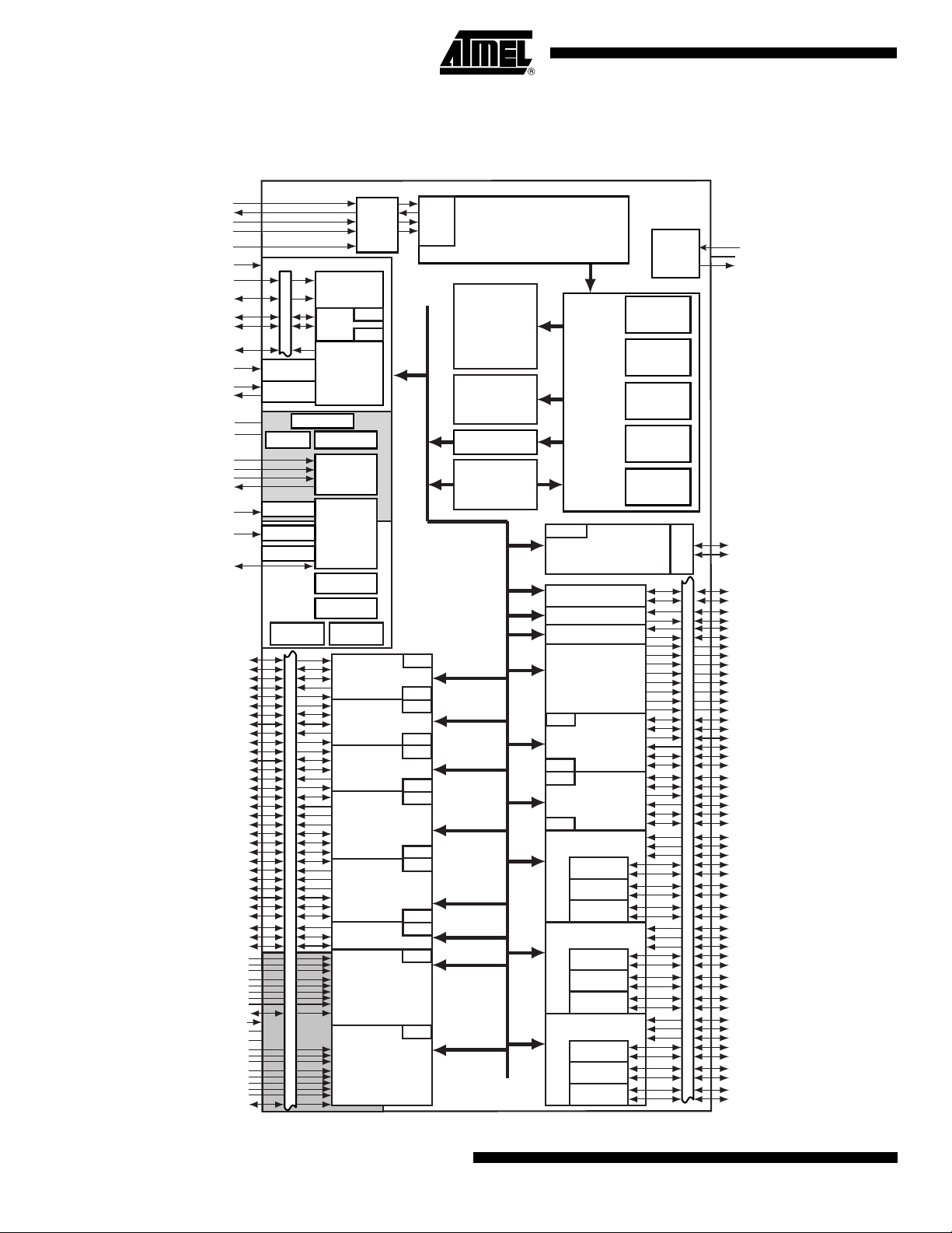
2. Block Diagram
Figure 2-1. AT91SAM7A3 Block Diagram
TDI
TDO
TMS
TCK
JTAGSEL
TST
FIQ
IRQ0-IRQ3
DRXD
DTXD
PCK0-PCK3
PLLRC
XIN
XOUT
GND
VDDBU
FWKUP
WKUP0
WKUP1
SHDW
VDDBU
VDD3V3
NRST
RXD0
TXD0
SCK0
RTS0
CTS0
RXD1
TXD1
SCK1
RTS1
CTS1
RXD2
TXD2
SCK2
RTS2
CTS2
SPI0_NPCS0
SPI0_NPCS1
SPI0_NPCS2
SPI0_NPCS3
SPI0_MISO
SPI0_MOSI
SPI0_SPCK
SPI1_NPCS0
SPI1_NPCS1
SPI1_NPCS2
SPI1_NPCS3
SPI1_MISO
SPI1_MOSI
SPI1_SPCK
MCCK
MCCDA
MCDA0-MCDA3
ADC0_AD0
ADC0_AD1
ADC0_AD2
ADC0_AD3
ADC0_AD4
ADC0_AD5
ADC0_AD6
ADC0_AD7
ADC0_ADTRG
ADVREFP
VDDANA
GND
ADC1_AD0
ADC1_AD1
ADC1_AD2
ADC1_AD3
ADC1_AD4
ADC1_AD5
ADC1_AD6
ADC1_AD7
ADC1_ADTRG
System Controller
PIO
PLL
OSC
GPBR
RCOSC
POR
POR
VDD1V8 POR
PIOA
PIO
AIC
DBGU
PMC
RTT
Shutdown
Controller
Reset
Controller
PIT
WDT
PIOB
JTAG
SCAN
PDC
PDC
USART0
USART1
USART2
SPI0
SPI1
MCI
ADC0
ADC1
PDC
PDC
PDC
PDC
PDC
PDC
PDC
PDC
PDC
PDC
PDC
PDC
PDC
PDC
ICE
Peripheral Bridge
Peripheral Data
APB
ARM7TDMI
Processor
FLASH
256K Bytes
SRAM
32K Bytes
Controller
19 channels
Memory
Controller
FIFO
USB Device
PWMC
PDC
PDC
PDC
PDC
Timer Counter
Timer Counter
Timer Counter
TWI
CAN0
CAN1
SSC0
SSC1
TC0
TC1
TC2
TC3
TC4
TC5
TC6
TC7
TC8
1.8 V
Voltage
Regulator
Embedded
Flash
Controller
Memory
Protection
Unit
Address
Decoder
Abort
Status
Misalignment
Detection
VDD3V3
GND
VDD1V8
DDM
PIO
DDP
TWD
TWCK
CANRX0
CANTX0
CANRX1
CANTX1
PWM0
PWM1
PWM2
PWM3
PWM4
PWM5
PWM6
PWM7
TF0
TK0
TD0
RD0
RK0
RF0
TF1
TK1
TD1
RD1
RK1
RF1
TCLK0
TCLK1
TCLK2
TIOA0
TIOB0
TIOA1
TIOB1
TIOA2
TIOB2
TCLK3
TCLK4
TCLK5
TIOA3
TIOB3
TIOA4
TIOB4
TIOA5
TIOB5
TCLK6
TCLK7
TCLK8
TIOA6
TIOB6
TIOA7
TIOB7
TIOA8
TIOB8
Transceiver
4
AT91SAM7A3 Preliminary
6042E–ATARM–14-Dec-06
Page 5

AT91SAM7A3 Preliminary
3. Signal Description
Table 3-1. Signal Description
Active
Signal Name Function Type
Power
VDD3V3
VDDBU Backup I/O Lines Power Supply Power 3V to 3.6V
VDDANA Analog Power Supply Power 3V to 3.6V
1.8V Voltage Regulator, I/O Lines and
Flash Power Supply
Power 3.0V to 3.6V
Level Comments
VDD1V8
VDDPLL 1.8V PLL Power Supply Power 1.65V to 1.95V
GND Ground Ground
XIN Main Oscillator Input Input
XOUT Main Oscillator Output Output
PLLRC PLL Filter Input
PCK0 - PCK3 Programmable Clock Output Output
SHDW Shut-Down Control Output Open Drain.
WKUP0 - WKUP1 Wake-Up Inputs Input Accept between 0V and VDDBU
FWKUP Force Wake Up Input
TCK Test Clock Input No pull-up resistor
TDI Test Data In Input No pull-up resistor
TDO Test Data Out Output
TMS Test Mode Select Input No pull-up resistor
JTAGSEL JTAG Selection Input Pull-down resistor
1.8V Voltage Regulator Output and Core
Power Supply
Clocks, Oscillators and PLLs
ICE and JTAG
Reset/Test
Power 1.85V typical
Accept between 0V and VDDBU
External pull-up resistor needed.
NRST Microcontroller Reset I/O Low
TST Test Mode Select Input High Pull-down resistor
Debug Unit
DRXD Debug Receive Data Input
DTXD Debug Transmit Data Output
6042E–ATARM–14-Dec-06
5
Page 6

Table 3-1. Signal Description (Continued)
Active
Signal Name Function Type
AIC
IRQ0 - IRQ3 External Interrupt Inputs Input
FIQ Fast Interrupt Input Input
PIO
PA0 - PA31 Parallel IO Controller A I/O Pulled-up input at reset
PB0 - PB29 Parallel IO Controller B I/O Pulled-up input at reset
Multimedia Card Interface
MCCK Multimedia Card Clock Output
MCCDA Multimedia Card A Command I/O
MCDA0 - MCDA3 Multimedia Card A Data I/O
USB Device Port
DDM USB Device Port Data - Analog
DDP USB Device Port Data + Analog
USART
SCK0 - SCK1 - SCK2 Serial Clock I/O
Level Comments
TXD0 - TXD1 - TXD2 Transmit Data I/O
RXD0 - RXD1 - RXD2 Receive Data Input
RTS0 - RTS1 - RTS2 Request To Send Output
CTS0 - CTS1 - CTS2 Clear To Send Input
Synchronous Serial Controller
TD0 - TD1 Transmit Data Output
RD0 - RD1 Receive Data Input
TK0 - TK1 Transmit Clock I/O
RK0 - RK1 Receive Clock I/O
TF0 - TF1 Transmit Frame Sync I/O
RF0 - RF1 Receive Frame Sync I/O
Timer/Counter
TCLK0 - TCLK8 External Clock Input Input
TIOA0 - TIOA8 I/O Line A I/O
TIOB0 - TIOB8 I/O Line B I/O
PWM Controller
PWM0 - PWM7 PWM Channels Output
6
AT91SAM7A3 Preliminary
6042E–ATARM–14-Dec-06
Page 7

AT91SAM7A3 Preliminary
Table 3-1. Signal Description (Continued)
Signal Name Function Type
SPI
Active
Level Comments
SPI0_MISO
SPI1_MISO
SPI0_MOSI
SPI1_MOSI
SPI0_SPCK
SPI1_SPCK
SPI0_NPCS0
SPI1_NPCS0
SPI0_NPCS1 - SPI0_NPCS3
SPI1_NPCS1 - SPI1_NPCS3
TWD Two-wire Serial Data I/O
TWCK Two-wire Serial Clock I/O
ADC0_AD0 - ADC0_AD7
ADC1_AD0 - ADC1_AD7
ADVREFP Analog Positive Reference Analog
ADC0_ADTRG
ADC1_ADTRG
Master In Slave Out I/O
Master Out Slave In I/O
SPI Serial Clock I/O
SPI Peripheral Chip Select 0 I/O Low
SPI Peripheral Chip Select Output Low
Two-wire Interface
Analog-to-Digital Converter
Analog Inputs Analog Digital pulled-up inputs at reset
ADC Trigger Input
CAN Controller
CANRX0-CANRX1 CAN Inputs Input
CANTX0-CANTX1 CAN Outputs Output
6042E–ATARM–14-Dec-06
7
Page 8

4. Package
4.1 100-lead LQFP Package Outline
Figure 4-1 shows the orientation of the 100-lead LQFP package. A detailed mechanical
description is given in the Mechanical Characteristics section of the full datasheet.
Figure 4-1. 100-lead LQFP Outline (Top View)
5175
76
100
50
26
125
8
AT91SAM7A3 Preliminary
6042E–ATARM–14-Dec-06
Page 9

AT91SAM7A3 Preliminary
4.2 Pinout
Table 4-1. Pinout in 100-lead LQFP Package
1 GND 26 VDDBU 51 PA20 76 PLLRC
2 NRST 27 FWKUP 52 PA21 77 VDDANA
3 TST 28 WKUP0 53 PA22 78 ADVREFP
4 PB13 29 WKUP1 54 PA23 79 GND
5 PB12 30 SHDW 55 PA24 80 PB14/ADC0_AD0
6 PB11 31 GND 56 PA25 81 PB15/ADC0_AD1
7 PB10 32 PA4 57 PA26 82 PB16/ADC0_AD2
8 PB9 33 PA5 58 PA27 83 PB17/ADC0_AD3
9 PB8 34 PA6 59 VDD1V8 84 PB18/ADC0_AD4
10 PB7 35 PA7 60 GND 85 PB19/ADC0_AD5
11 PB6 36 PA8 61 VDD3V3 86 PB20/ADC0_AD6
12 PB5 37 PA9 62 PA28 87 PB21/ADC0_AD7
13 PB4 38 VDD3V3 63 PA29 88 VDD3V3
14 PB3 39 GND 64 PA30 89 PB22/ADC1_AD0
15 VDD3V3 40 VDD1V8 65 PA31 90 PB23/ADC1_AD1
16 GND 41 PA10 66 JTAGSEL 91 PB24/ADC1_AD2
17 VDD1V8 42 PA11 67 TDI 92 PB25/ADC1_AD3
18 PB2 43 PA12 68 TMS 93 PB26/ADC1_AD4
19 PB1 44 PA13 69 TCK 94 PB27/ADC1_AD5
20 PB0 45 PA14 70 TDO 95 PB28/ADC1_AD6
21 PA0 46 PA15 71 GND 96 PB29/ADC1_AD7
22 PA1 47 PA16 72 VDDPLL 97 DDM
23 PA2 48 PA17 73 XOUT 98 DDP
24 PA3 49 PA18 74 XIN 99 VDD1V8
25 GND 50 PA19 75 GND 100 VDD3V3
6042E–ATARM–14-Dec-06
9
Page 10

5. Power Considerations
5.1 Power Supplies
The AT91SAM7A3 has five types of power supply pins:
• VDD3V3 pins. They power the voltage regulator, the I/O lines, the Flash and the USB
transceivers; voltage ranges from 3.0V to 3.6V, 3.3V nominal.
• VDD1V8 pins. They are the outputs of the 1.8V voltage regulator and they power the logic
of the device.
• VDDPLL pin. It powers the PLL; voltage ranges from 1.65V to 1.95V, 1.8V typical. They can
be connected to the VDD1V8 pin with decoupling capacitor.
• VDDBU pin. It powers the Slow Clock oscillator and the Real Time Clock, as well as a part
of the System Controller; ranges from 3.0V and 3.6V, 3.3V nominal.
• VDDANA pin. It powers the ADC; ranges from 3.0V and 3.6V, 3.3V nominal.
No separate ground pins are provided for the different power supplies. Only GND pins are provided and should be connected as shortly as possible to the system ground plane.
5.2 Voltage Regulator
The AT91SAM7A3 embeds a voltage regulator that consumes less than 120 µA static current
and draws up to 130 mA of output current.
Adequate output supply decoupling is mandatory for VDD1V8 (pin 99)to reduce ripple and
avoid oscillations. The best way to achieve this is to use two capacitors in parallel: one external 470 pF (or 1 nF) NPO capacitor must be connected between VDD1V8 and GND as close
to the chip as possible. One external 3.3 µF (or 4.7 µF) X7R capacitor must be connected
between VDD1V8 and GND.
All other VDD1V8 pins must be externally connected and have a proper decoupling capacitor
(at least 100 nF).
Adequate input supply decoupling is mandatory for VDD3V3 (pin 100) in order to improve startup stability and reduce source voltage drop. The input decoupling capacitor should be placed
close to the chip. For example, two capacitors can be used in parallel: 100 nF NPO and 4.7 µF
X7R.
All other VDD3V3 pins must be externally connected and have a proper decoupling capacitor
(at least 100 nF).
10
AT91SAM7A3 Preliminary
6042E–ATARM–14-Dec-06
Page 11
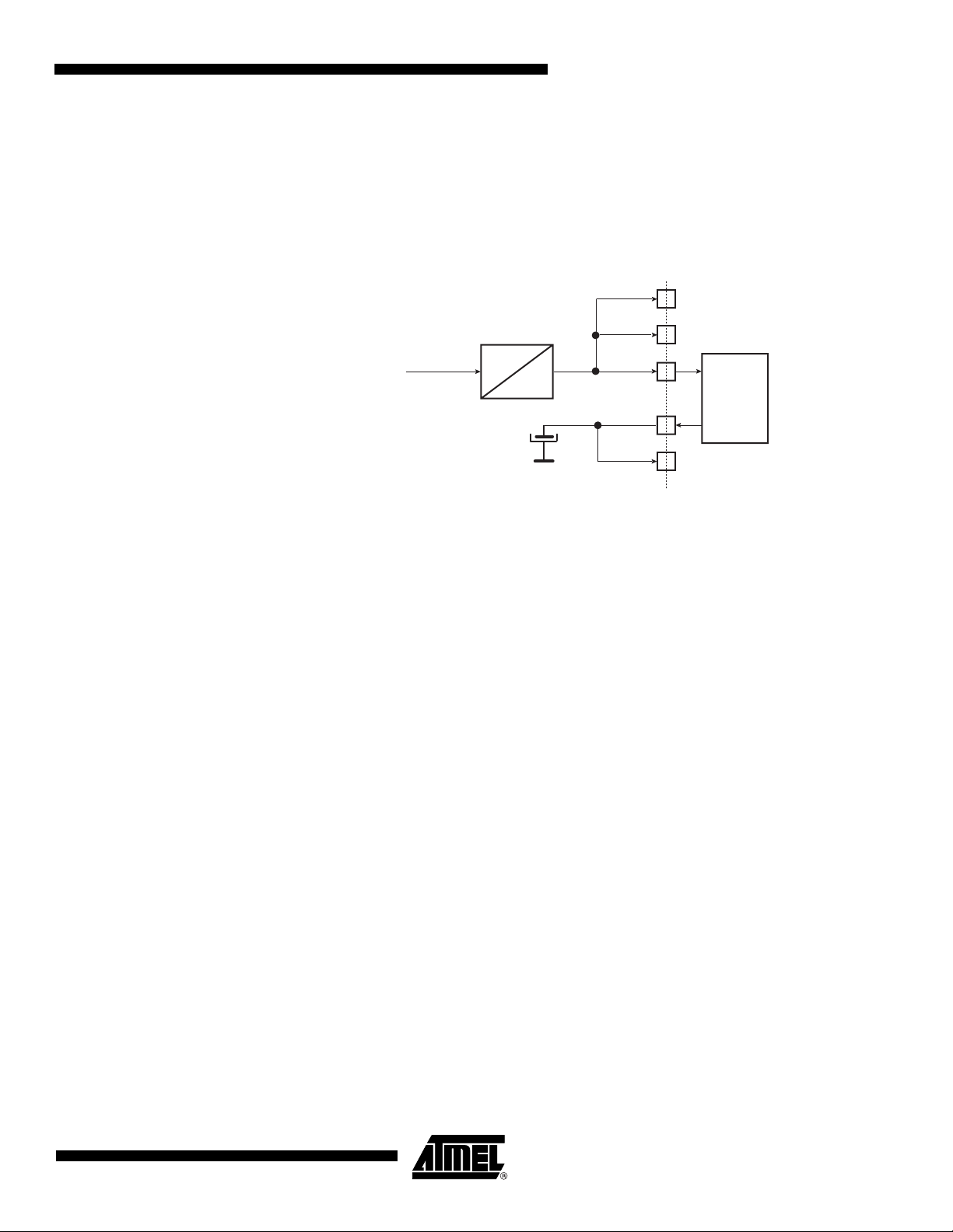
5.3 Typical Powering Schematics
5.3.1 3.3V Single Supply
The AT91SAM7A3 supports a 3.3V single supply mode. The internal regulator is connected to
the 3.3V source and its output feeds VDDPLL. Figure 5-1 shows the power schematics to be
used for USB bus-powered systems.
Figure 5-1. 3.3V System Single Power Supply Schematics
AT91SAM7A3 Preliminary
VDDBU
USB Connector
up to 5.5V
DC/DC Converter
3.3V
VDDANA
VDD3V3
Voltage
Regulator
VDD1V8
VDDPLL
6042E–ATARM–14-Dec-06
11
Page 12

6. I/O Lines Considerations
6.1 JTAG Port Pins
TMS, TDI and TCK are schmitt trigger inputs. TMS and TCK are 5V-tolerant, TDI is not. TMS,
TDI and TCK do not integrate any resistors and have to be pulled-up externally.
TDO is an output, driven at up to VDD3V3.
The JTAGSEL pin is used to select the JTAG boundary scan when asserted at a high level.
The JTAGSEL pin integrates a permanent pull-down resistor so that it can be left unconnected
for normal operations.
6.2 Test Pin
The TST pin is used for manufacturing tests and integrates a pull-down resistor so that it can
be left unconnected for normal operations. Driving this line at a high level leads to unpredictable results.
6.3 Reset Pin
The NRST pin is bidirectional. It is handled by the on-chip reset controller and can be driven
low to provide a reset signal to the external components or asserted low externally to reset the
microcontroller. There is no constraint on the length of the reset pulse, and the reset controller
can guarantee a minimum pulse length. This allows connection of a simple push-button on the
NRST pin as system user reset, and the use of the NRST signal to reset all the components of
the system.
6.4 PIO Controller A and B Lines
All the I/O lines PA0 to PA31 and PB0 to PB29 are 5V-tolerant and all integrate a programmable pull-up resistor. Programming of this pull-up resistor is performed independently for each
I/O line through the PIO Controllers.
5V-tolerant means that the I/O lines can drive voltage level according to VDD3V3, but can be
driven with a voltage at up to 5.5V. However, driving an I/O line with a voltage over VDD3V3
while the programmable pull-up resistor is enabled creates a current path through the pull-up
resistor from the I/O line to VDDIO. Care should be taken, especially at reset, as all the I/O
lines default as inputs with pull-up resistor enabled at reset.
6.5 Shutdown Logic Pins
The SHDW pin is an open drain output. It can be tied to VDDBU with an external pull-up
resistor.
The FWUP, WKUP0 and WKUP1 pins are input-only. They can accept voltages only between
0V and VDDBU. It is recommended to tie these pins either to GND or to VDDBU with an external resistor.
6.6 I/O Line Drive Levels
All the I/O lines can draw up to 2 mA.
12
AT91SAM7A3 Preliminary
6042E–ATARM–14-Dec-06
Page 13

7. Processor and Architecture
7.1 ARM7TDMI Processor
• RISC Processor Based on ARMv4T Von Neumann Architecture
– Runs at up to 60 MHz, providing 0.9 MIPS/MHz
• Two instruction sets
– ARM high-performance 32-bit Instruction Set
– Thumb high code density 16-bit Instruction Set
• Three-stage pipeline architecture
– Instruction Fetch (F)
– Instruction
– Execute (E)
7.2 Debug and Test Features
• Integrated EmbeddedICE™ (embedded in-circuit emulator)
– Two watchpoint units
– Test access port accessible through a JTAG protocol
– Debug communication channel
• Debug Unit
–Two-pin UART
– Debug communication channel interrupt handling
– Chip ID Register
• IEEE1149.1 JTAG Boundary-scan on all digital pins
AT91SAM7A3 Preliminary
Decode (D)
7.3 Memory Controller
• Bus Arbiter
• Address Decoder Provides Selection Signals for
• Abort Status Registers
• Misalignment Detector
• Remap Command
• 16-area Memory Protection Unit
– Handles requests from the ARM7TDMI and the Peripheral Data Controller
– Three internal 1Mbyte memory areas
– One 256 Mbyte embedded peripheral area
– Source, Type and all parameters of the access leading to an abort are saved
– Facilitates debug by detection of bad pointers
– Alignment checking of all data accesses
– Abort generation in case of misalignment
– Remaps the Internal SRAM in place of the embedded non-volatile memory
– Allows handling of dynamic exception vectors
– Individually programmable size between 1K Bytes and 1M Bytes
6042E–ATARM–14-Dec-06
13
Page 14

– Individually programmable protection against write and/or user access
– Peripheral protection against write and/or user access
• Embedded Flash Controller
– Embedded Flash interface, up to three programmable wait states
– Read-optimized interface, buffering and anticipating the 16-bit requests, reducing
the required wait states
– Password-protected program, erase and lock/unlock sequencer
– Automatic consecutive programming, erasing and locking operations
– Interrupt generation in case of forbidden operation
7.4 Peripheral DMA Controller
• Handles data transfer between peripherals and memories
• Nineteen Channels
– Two for each USART
– Two for the Debug Unit
– Two for each Serial Synchronous Controller
– Two for each Serial Peripheral Interface
– One for the Multimedia Card Interface
– One for each Analog-to-Digital Converter
• Low bus arbitration overhead
– One Master Clock cycle needed for a transfer from memory to peripheral
– Two Master Clock cycles needed for a transfer from peripheral to memory
• Next Pointer management for reducing interrupt latency requirements
14
AT91SAM7A3 Preliminary
6042E–ATARM–14-Dec-06
Page 15

8. Memory
8.1 Embedded Memories
• 256 Kbytes of Flash Memory
• 32 Kbytes of Fast SRAM
AT91SAM7A3 Preliminary
– 1024 pages of 256 bytes.
– Fast access time, 30 MHz single cycle access in worst case conditions.
– Page programming time: 6 ms, including page auto-erase
– Full erase time: 15 ms
– 10,000 write cycles, 10-year data retention capability
– 16 lock bits, each protecting 16 pages
– Single-cycle access at full speed
6042E–ATARM–14-Dec-06
15
Page 16
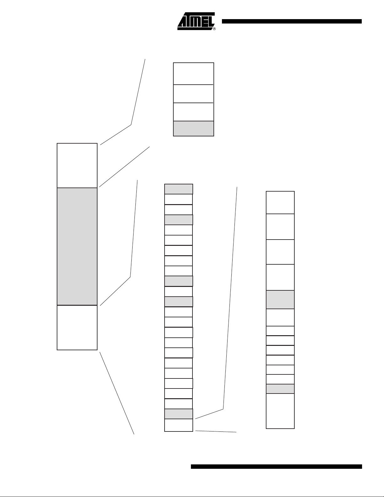
Figure 8-1. AT91SAM7A3 Memory Mapping
0x0000 0000
0x000F FFF
0x0010 0000
0x001F FFF
0x0020 0000
0x002F FFF
0x0030 0000
Address Memory Space
0x0000 0000
0x0FFF FFFF
Internal Memory Mapping
Flash before Remap
SRAM after Remap
Internal Flash
Internal SRAM
Reserved
1 MBytes
1 MBytes
1 MBytes
252 MBytes
0x0FFF FFFF
0x1000 0000
0xEFFF FFFF
0xF000 0000
0xFFFF FFFF
Internal Memories
Undefined
(Abort)
Internal Peripherals
256 MBytes
14 x 256 MBytes
3,584 MBytes
256 MBytes
0xF000 0000
0xFFF7 FFFF
0xFFF8 0000
0xFFF8 3FFF
0xFFF8 4000
0xFFF8 7FFF
0xFFF8 8000
0xFFF9 FFFF
0xFFFA 0000
0xFFFA 3FFF
0xFFFA 4000
0xFFFA 7FFF
0xFFFA 8000
0xFFFA BFFF
0xFFFA C000
0xFFFA FFFF
0xFFFB 0000
0xFFFB 3FFF
0xFFFB 4000
0xFFFB 7FFF
0xFFFB 8000
0xFFFB BFFF
0xFFFB C000
0xFFFB FFFF
0xFFFC 0000
0xFFFC 3FFF
0xFFFC 4000
0xFFFC 7FFF
0xFFFC 8000
0xFFFC BFFF
0xFFFC C000
0xFFFC FFFF
0xFFFD 0000
0xFFFD 3FFF
0xFFFD 4000
0xFFFD 7FFF
0xFFFD 8000
0xFFFD BFFF
0xFFFD C000
0xFFFD FFFF
0xFFFE 0000
0xFFFE 3FFF
0xFFFE 4000
0xFFFE 7FFF
0xFFFE 8000
0xFFFF EFFF
0xFFFF F000
0xFFFF FFFF
Peripheral Mapping
Reserved
CAN0
CAN1
Reserved
TC0, TC1, TC2
TC3, TC4, TC5
TC6, TC7, TC8
MCI
UDP
Reserved
TWI
Reserved
USART0
USART1
USART2
PWMC
SSC0
SSC1
ADC0
ADC1
SPI0
SPI1
Reserved
SYSC
16 Kbytes
16 Kbytes
16 Kbytes
16 Kbytes
16 Kbytes
16 Kbytes
16 Kbytes
16 Kbytes
16 Kbytes
16 Kbytes
16 Kbytes
16 Kbytes
16 Kbytes
16 Kbytes
16 Kbytes
16 Kbytes
16 Kbytes
16 Kbytes
0xFFFF F000
0xFFFF F1FF
0xFFFF F200
0xFFFF F3FF
0xFFFF F400
0xFFFF F5FF
0xFFFF F600
0xFFFF F7FF
0xFFFF F800
0xFFFF FBFF
0xFFFF FC00
0xFFFF FCFF
0xFFFF FD00
0xFFFF FD0F
0xFFFF FD10
0xFFFF FD1F
0xFFFF FD20
0xFFFF FC2F
0xFFFF FD30
0xFFFF FC3F
0xFFFF FD40
0xFFFF FD4F
0xFFFF FD50
0xFFFF FC58
0xFFFF FD59
0xFFFF FEFF
0xFFFF FF00
0xFFFF FFFF
System Controller Mapping
AIC
DBGU
PIOA
PIOB
Reserved
PMC
RSTC
SHDWC
RTT
PIT
WDT
GPBR
Reserved
MC
512 Bytes/128 registers
512 Bytes/128 registers
512 Bytes/128 registers
512 Bytes/128 registers
256 Bytes/64 registers
16 Bytes/4 registers
16 Bytes/4 registers
16 Bytes/4 registers
16 Bytes/4 registers
8 Bytes/2 registers
general purpose backup registers
256 Bytes/64 registers
16
AT91SAM7A3 Preliminary
6042E–ATARM–14-Dec-06
Page 17

8.2 Memory Mapping
8.2.1 Internal SRAM
The AT91SAM7A3 embeds a high-speed 32-Kbyte SRAM bank. After reset and until the
Remap Command is performed, the SRAM is only accessible at address 0x0020 0000. After
Remap, the SRAM also becomes available at address 0x0.
8.2.2 Internal Flash
The AT91SAM7A3 features one bank of 256 Kbytes of Flash. The Flash is mapped to address
0x0010 0000. It is also accessible at address 0x0 after the reset and before the Remap
Command.
Figure 8-2. Internal Memory Mapping
256M Bytes
0x0000 0000
0x000F FFFF
0x0010 0000
0x001F FFFF
0x0020 0000
0x002F FFFF
0x0030 0000
AT91SAM7A3 Preliminary
Flash Before Remap
SRAM After Remap
Internal Flash
Internal SRAM
1M Bytes
1M Bytes
1M Bytes
8.3 Embedded Flash
8.3.1 Flash Overview
The Flash block of the AT91SAM7A3 is organized in 1024 pages of 256 bytes. It reads as
65,536 32-bit words.
The Flash block contains a 256-byte write buffer, accessible through a 32-bit interface.
When Flash is not used (read or write access), it is automatically put into standby mode.
8.3.2 Embedded Flash Controller
The Embedded Flash Controller (EFC) manages accesses performed by the masters of the
system. It enables reading the Flash and writing the write buffer. It also contains a User Interface mapped within the Memory Controller on the APB. The User Interface allows:
• programming of the access parameters of the Flash (number of wait states, timings, etc.)
• starting commands such as full erase, page erase, page program, NVM bit set, NVM bit
clear, etc.
• getting the end status of the last command
• getting error status
• programming interrupts on the end of the last commands or on errors
0x0FFF FFFF
Undefined Areas
(Abort)
253M Bytes
6042E–ATARM–14-Dec-06
17
Page 18

8.3.3 Lock Regions
The Embedded Flash Controller also provides a dual 32-bit Prefetch Buffer that optimizes 16bit access to the Flash. This is particularly efficient when the processor is running in Thumb
mode.
The Embedded Flash Controller manages 16 lock bits to protect 16 regions of the Flash
against inadvertent Flash erasing or programming commands.
The AT91SAM7A3 has 16 lock regions. Each lock region contains 16 pages of 256 bytes.
Each lock region has a size of 4 Kbytes, thus only the first 64 Kbytes can be locked.
The 16 NVM bits are software programmable through the EFC User Interface. The command
“Set Lock Bit” activates the protection. The command “Clear Lock Bit” unlocks the lock region.
18
AT91SAM7A3 Preliminary
6042E–ATARM–14-Dec-06
Page 19

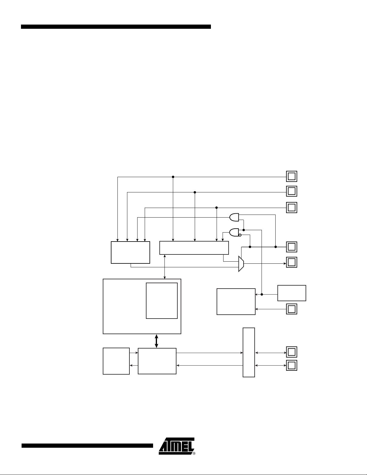
9. System Controller
The System Controller manages all vital blocks of the microcontroller: interrupts, clocks,
power, time, debug and reset.
The System Controller peripherals are all mapped to the highest 4K bytes of address space,
between addresses 0xFFFF F000 and 0xFFFF FFFF. Each peripheral has an address space
of up to 512 Bytes, representing up to 128 registers.
Figure 9-1 on page 20 shows the System Controller Block Diagram.
Figure 8-1 on page 16 shows the mapping of the User Interface of the System Controller
peripherals. Note that the Memory Controller configuration user interface is also mapped
within this address space.
AT91SAM7A3 Preliminary
6042E–ATARM–14-Dec-06
19
Page 20
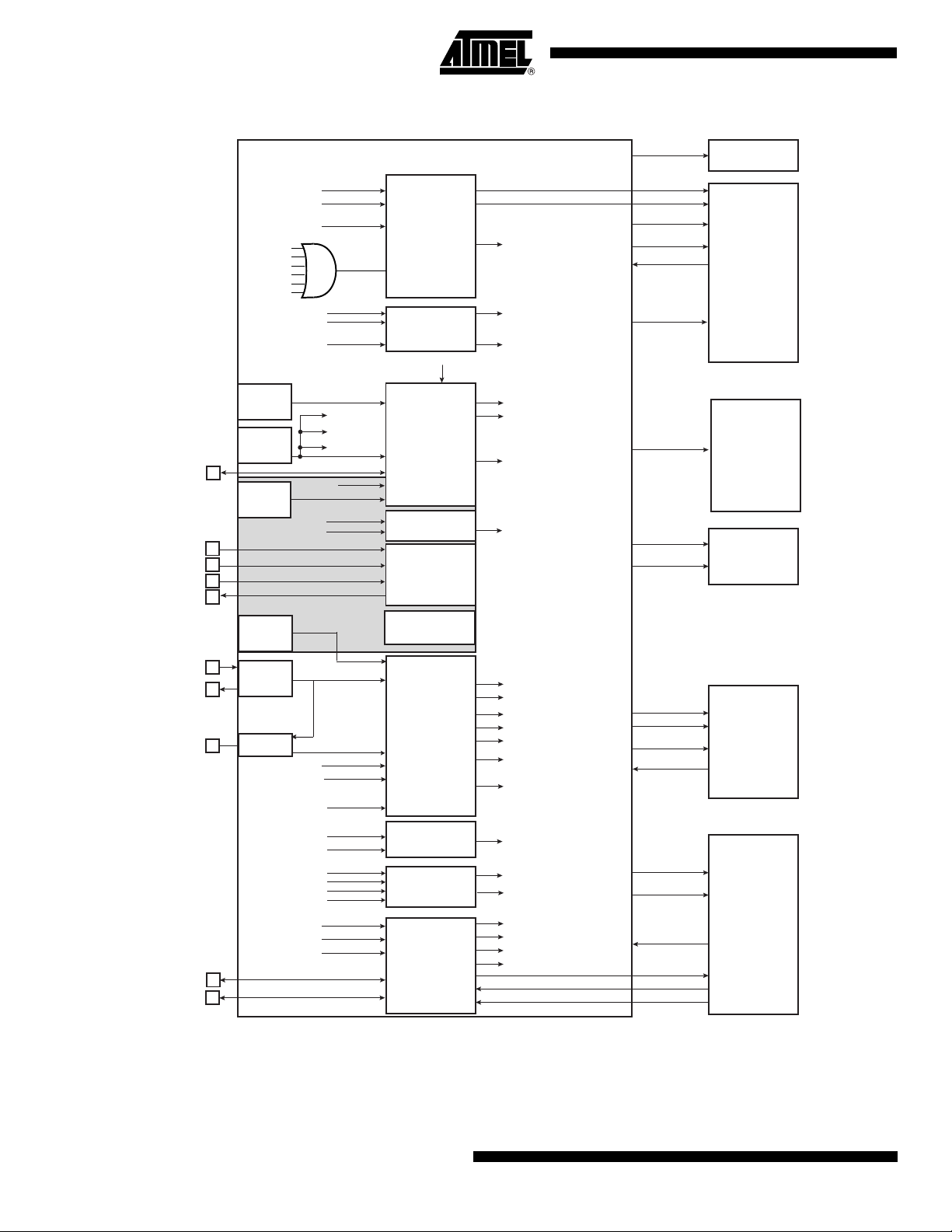
Figure 9-1. System Controller Block Diagram
NRST
FWKUP
WKUP0
WKUP1
SHDW
irq0-irq1-irq2-irq3
periph_irq[2..27]
pit_irq
rtt_irq
wdt_irq
dbgu_irq
pmc_irq
rstc_irq
periph_nreset
dbgu_rxd
VDD3V3
POR
VDD1V8
POR
VDDBU
POR
periph_nreset
VDDBU Powered
RCOSC
fiq
MCK
SLCK
SLCK
SLCK
ice_nreset
jtag_nreset
flash_poe
System Controller
Advanced
Interrupt
Controller
Debug
Unit
wdt_fault
WDRPROC
Reset
Controller
Real-Time
Timer
Shutdown
Controller
4 General-Purpose
Backup Regs
int
dbgu_irq
dbgu_txd
periph_nreset
proc_nreset
rstc_irq
VDD1V8 Powered
rtt_irq
jtag_nreset
nirq
nfiq
proc_nreset
PCK
debug
ice_nreset
proc_nreset
MCK
proc_nreset
Boundary Scan
TAP Controller
ARM7TDMI
Embedded Flash
Memory
Controller
XIN
XOUT
PLLRC
PA0-PA31
PB0-PB29
MAIN
OSC
PLL
periph_nreset
periph_nreset
proc_nreset
periph_nreset
periph_clk[2..3]
dbgu_rxd
MAINCK
int
MCK
debug
SLCK
debug
idle
PLLCK
9.1 System Controller Mapping
Power
Management
Controller
Periodic
Interval
Timer
Watchdog
Timer
PIOs
Controller
periph_clk[2..27]
pck[0-3]
PCK
UDPCK
MCK
pmc_irq
idle
pit_irq
wdt_irq
wdt_fault
WDRPROC
periph_irq{2..3]
irq0-irq1-irq2-irq3
fiq
dbgu_txd
UDPCK
periph_clk[27]
periph_nreset
periph_irq[27]
periph_clk[4..26]
periph_nreset
periph_irq[4..26]
in
out
enable
USB Device
Por t
Embedded
Peripherals
20
AT91SAM7A3 Preliminary
6042E–ATARM–14-Dec-06
Page 21
9.2 Reset Controller
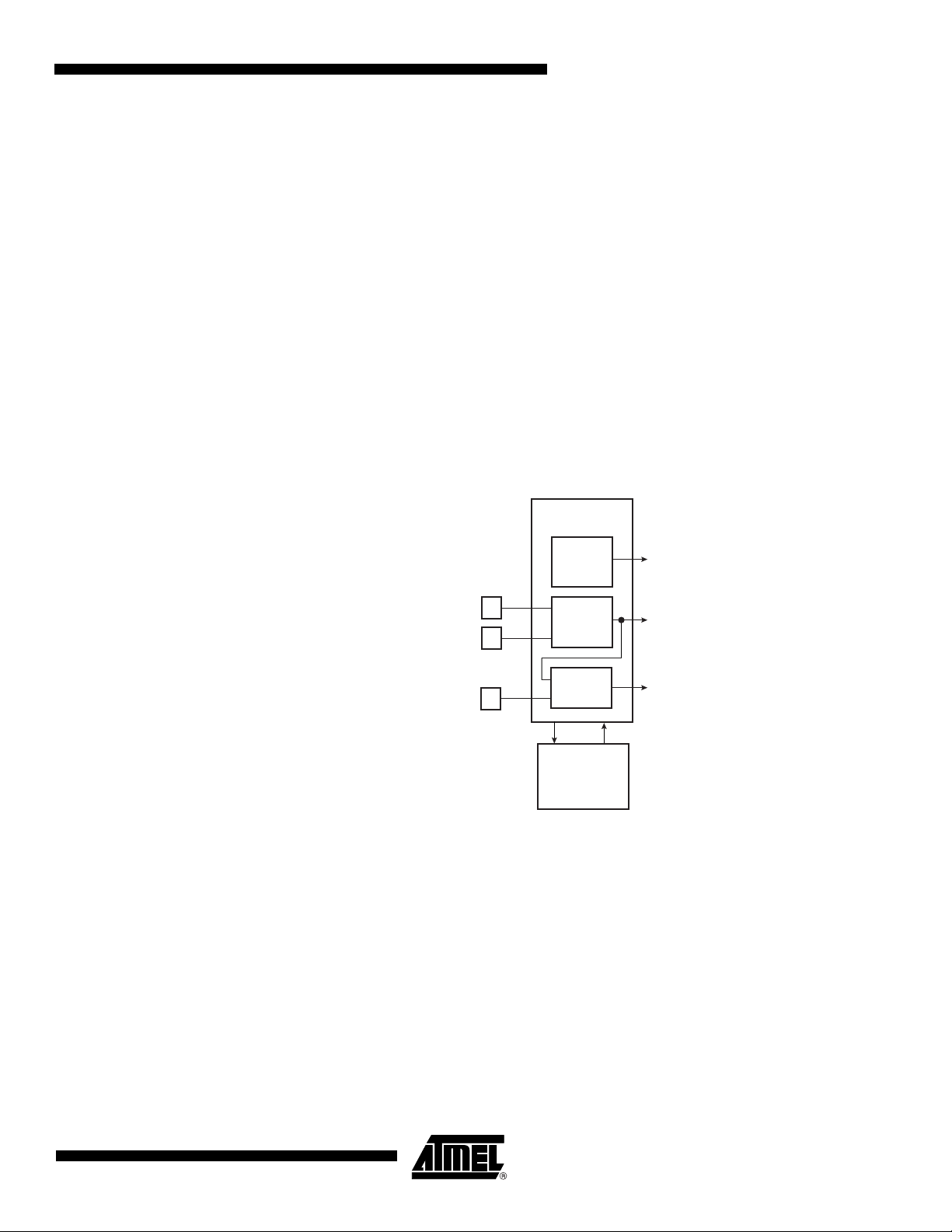
9.3 Clock Generator
AT91SAM7A3 Preliminary
The Reset Controller is based on three power-on reset cells. It gives the status of the last
reset, indicating whether it is a general reset, a wake-up reset, a software reset, a user reset
or a watchdog reset. In addition, it controls the internal resets and the NRST pin output. It
shapes a signal on the NRST line, guaranteeing that the length of the pulse meets any
requirement.
The Clock Generator embeds one low-power RC Oscillator, one Main Oscillator and one PLL
with the following characteristics:
– RC Oscillator ranges between 22 KHz and 42 KHz
– Main Oscillator frequency ranges between 3 and 20 MHz
– Main Oscillator can be bypassed
– PLL output ranges between 80 and 220 MHz
It provides SLCK, MAINCK and PLLCK.
Figure 9-2. Clock Generator Block Diagram
Clock Generator
9.4 Power Management Controller
The Power Management Controller uses the Clock Generator outputs to provide:
– the Processor Clock PCK
– the Master Clock MCK
– the USB Clock UDPCK
– all the peripheral clocks, independently controllable
– four programmable clock outputs
The Master Clock (MCK) is programmable from a few hundred Hz to the maximum operating
frequency of the device.
XIN
XOUT
PLLRC
Embedded
RC
Oscillator
Main
Oscillator
PLL and
Divider
Power
Management
Controller
Slow Clock
SLCK
Main Clock
MAINCK
PLL Clock
PLLCK
ControlStatus
6042E–ATARM–14-Dec-06
The Processor Clock (PCK) switches off when entering processor idle mode, thereby reducing
power consumption while waiting an interrupt.
21
Page 22
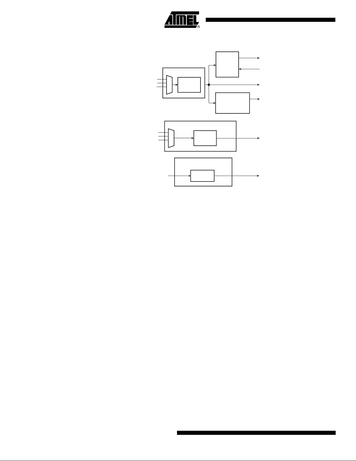
Figure 9-3. Power Management Controller Block Diagram
9.5 Advanced Interrupt Controller
• Controls the interrupt lines (nIRQ and nFIQ) of the ARM Processor
• Individually maskable and vectored interrupt sources
– Source 0 is reserved for the Fast Interrupt Input (FIQ)
– Source 1 is reserved for system peripherals (ST, PMC, DBGU, etc.)
– Other sources control the peripheral interrupts or external interrupts
– Programmable edge-triggered or level-sensitive internal sources
– Programmable positive/negative edge-triggered or high/low level-sensitive
external sources (FIQ, IRQ)
• 8-level Priority Controller
– Drives the normal interrupt nIRQ of the processor
– Handles priority of the interrupt sources
– Higher priority interrupts can be served during service of a lower priority interrupt
• Vectoring
– Optimizes interrupt service routine branch and execution
– One 32-bit vector register per interrupt source
– Interrupt vector register reads the corresponding current interrupt vector
• Protect Mode
– Easy debugging by preventing automatic operations
•Fast Forcing
– Permits redirecting any interrupt source on the fast interrupt
• General Interrupt Mask
– Provides processor synchronization on events without triggering an interrupt
SLCK
MAINCK
PLLCK
SLCK
MAINCK
PLLCK
Master Clock Controller
/1,/2,/4,...,/64
Programmable Clock Controller
PLLCK
Prescaler
Prescaler
/1,/2,/4,...,/64
USB Clock Controller
ON/OFF
Divider
/1,/2,/4
Processor
Clock
Controller
Idle Mode
Peripherals
Clock Controller
ON/OFF
PCK
int
MCK
periph_clk[2..26]
pck[0..3]
UDPCK
22
AT91SAM7A3 Preliminary
6042E–ATARM–14-Dec-06
Page 23

9.6 Debug Unit
AT91SAM7A3 Preliminary
• Comprises
– One two-pin UART
– One interface for the Debug Communication Channel (DCC) support
– One set of chip ID registers
– One interface allowing ICE access prevention
•Two-pin UART
– USART-compatible user interface
– Programmable baud rate generator
– Parity, framing and overrun error
– Automatic Echo, Local Loopback and Remote Loopback Channel Modes
• Debug Communication Channel Support
– Offers visibility of COMMRX and COMMTX signals from the ARM Processor
• Chip ID Registers
– Identification of the device revision, sizes of the embedded memories, set of
peripherals
– Chip ID is 0x260A0941 (Version 1)
9.7 Period Interval Timer
• 20-bit programmable counter plus 12-bit interval counter
9.8 Watchdog Timer
• 12-bit key-protected Programmable Counter running on prescaled SLCK
• Provides reset or interrupt signals to the system
• Counter may be stopped while the processor is in debug state or in idle mode
9.9 Real-time Timer
• 32-bit free-running counter with alarm
• Programmable 16-bit prescaler for SCLK accuracy compensation
9.10 Shutdown Controller
• Software programmable assertion of the SHDW open-drain pin
• De-assertion programmable with the pins WKUP0, WKUP1 and FWKUP
9.11 PIO Controllers A and B
• The PIO Controllers A and B respectively control 32 and 30 programmable I/O Lines
• Fully programmable through Set/Clear Registers
• Multiplexing of two peripheral functions per I/O Line
• For each I/O Line (whether assigned to a peripheral or used as general purpose I/O)
– Input change interrupt
– Half a clock period Glitch filter
– Multi-drive option enables driving in open drain
6042E–ATARM–14-Dec-06
23
Page 24

– Programmable pull up on each I/O line
– Pin data status register, supplies visibility of the level on the pin at any time
• Synchronous output, provides Set and Clear of several I/O lines in a single write
24
AT91SAM7A3 Preliminary
6042E–ATARM–14-Dec-06
Page 25

10. Peripherals
10.1 Peripheral Mapping
Each User Peripheral is allocated 16K bytes of address space.
Figure 10-1. User Peripherals Mapping
0xF000 0000
0xFFF7 FFFF
0xFFF8 0000
0xFFF8 3FFF
0xFFF8 4000
0xFFF8 7FFF
0xFFF8 8000
0xFFF9 FFFF
0xFFFA 0000
0xFFFA 3FFF
0xFFFA 4000
0xFFFA 7FFF
0xFFFA 8000
0xFFFA BFFF
0xFFFA C000
0xFFFA FFFF
0xFFFB 0000
0xFFFB 3FFF
0xFFFB 4000
0xFFFB 7FFF
0xFFFB 8000
0xFFFB BFFF
0xFFFB C000
0xFFFB FFFF
0xFFFC 0000
0xFFFC 3FFF
0xFFFC 4000
0xFFFC 7FFF
0xFFFC 8000
0xFFFC BFFF
0xFFFC C000
0xFFFC FFFF
0xFFFD 0000
0xFFFD 3FFF
0xFFFD 4000
0xFFFD 7FFF
0xFFFD 8000
0xFFFD BFFF
0xFFFD C000
0xFFFD FFFF
0xFFFE 0000
0xFFFE 3FFF
0xFFFE 4000
0xFFFE 7FFF
0xFFFE 8000
0xFFFE FFFF
AT91SAM7A3 Preliminary
PeripheralAddress
Reserved
CAN0 CAN Controller 0 16K Bytes
CAN1 CAN Controller 1
Reserved
TC0, TC1, TC2 Timer/Counter 0, 1 and 2
TC3, TC4, TC5 Timer/Counter 3, 4 and 5
TC6, TC7, TC8 Timer/Counter 6, 7 and 8
MCI Multimedia Card Interface
UDP USB Device Port
Reserved
TWI Two-Wire Interface
Reserved
USART0 Universal Synchronous Asynchronous
USART1 Universal Synchronous Asynchronous
USART2 Universal Synchronous Asynchronous
PWMC
SSC0 Serial Synchronous Controller 0
SSC1 Serial Synchronous Controller 1
ADC0 Analog-to-Digital Converter 0
ADC1 Analog-to-Digital Converter 1
SPI0 Serial Peripheral Interface 0
SPI1 Serial Peripheral Interface 1
Reserved
Peripheral Name
Receiver Transmitter 0
Receiver Transmitter 1
Receiver Transmitter 1
PWM Controller
Size
16K Bytes
16K Bytes
16K Bytes
16K Bytes
16K Bytes
16K Bytes
16K Bytes
16K Bytes
16K Bytes
16K Bytes
16K Bytes
16K Bytes
16K Bytes
16K Bytes
16K Bytes
16K Bytes
16K Bytes
6042E–ATARM–14-Dec-06
25
Page 26

10.2 Peripheral Multiplexing on PIO Lines
The AT91SAM7A3 features two PIO controllers, PIOA and PIOB, which multiplex the I/O lines
of the peripheral set.
PIO Controllers A and B control respectively 32 and 30 lines. Each line can be assigned to one
of two peripheral functions, A or B. Some of them can also be multiplexed with Analog Input of
both ADC Controllers.
Table 10-1 on page 27 and Table 10-2 on page 28 define how the I/O lines of the peripherals
A, B or Analog Input are multiplexed on the PIO Controllers A and B. The two columns “Function” and “Comments” have been inserted for the user’s own comments; they may be used to
track how pins are defined in an application.
Note that some peripheral functions that are output only may be duplicated within both tables.
At reset, all I/O lines are automatically configured as input with the programmable pull-up
enabled, so that the device is maintained in a static state as soon as a reset occurs.
26
AT91SAM7A3 Preliminary
6042E–ATARM–14-Dec-06
Page 27

AT91SAM7A3 Preliminary
10.3 PIO Controller A Multiplexing
Table 10-1. Multiplexing on PIO Controller A
PIO Controller A Application Usage
I/O Line Peripheral A Peripheral B Comment Function Comments
PA0 TWD ADC0_ADTRG
PA1 TWCK ADC1_ADTRG
PA 2 R X D 0
PA 3 T X D 0
PA4 SCK0 SPI1_NPSC0
PA5 RTS0 SPI1_NPCS1
PA6 CTS0 SPI1_NPCS2
PA7 RXD1 SPI1_NPCS3
PA8 TXD1 SPI1_MISO
PA9 RXD2 SPI1_MOSI
PA10 TXD2 SPI1_SPCK
PA11 SPI0_NPCS0
PA12 SPI0_NPCS1 MCDA1
PA13 SPI0_NPCS2 MCDA2
PA14 SPI0_NPCS3 MCDA3
PA15 SPI0_MISO MCDA0
PA16 SPI0_MOSI MCCDA
PA17 SPI0_SPCK MCCK
PA18 PWM0 PCK0
PA19 PWM1 PCK1
PA20 PWM2 PCK2
PA21 PWM3 PCK3
PA 22 P W M 4 I R Q 0
PA 23 P W M 5 I R Q 1
PA 24 P W M 6 T C L K4
PA 25 P W M 7 T C L K5
PA26 CANRX0
PA27 CANTX0
PA28 CANRX1 TCLK3
PA29 CANTX1 TCLK6
PA30 DRXD TCLK7
PA 31 D T X D T C L K8
6042E–ATARM–14-Dec-06
27
Page 28

10.4 PIO Controller B Multiplexing
Table 10-2. Multiplexing on PIO Controller B
PIO Controller B Application Usage
I/O Line Peripheral A Peripheral B Comment Function Comments
PB0 IRQ2 PWM5
PB1 IRQ3 PWM6
PB2 TF0 PWM7
PB3 TK0 PCK0
PB4 TD0 PCK1
PB5 RD0 PCK2
PB6 RK0 PCK3
PB7 RF0 CANTX1
PB8 FIQ TF1
PB9 TCLK0 TK1
PB10 TCLK1 RK1
PB11 TCLK2 RF1
PB12 TIOA0 TD1
PB13 TIOB0 RD1
PB14 TIOA1 PWM0 ADC0_AD0
PB15 TIOB1 PWM1 ADC0_AD1
PB16 TIOA2 PWM2 ADC0_AD2
PB17 TIOB2 PWM3 ADC0_AD3
PB18 TIOA3 PWM4 ADC0_AD4
PB19 TIOB3 SPI1_NPCS1 ADC0_AD5
PB20 TIOA4 SPI1_NPCS2 ADC0_AD6
PB21 TIOB4 SPI1_NPCS3 ADC0_AD7
PB22 TIOA5 ADC1_AD0
PB23 TIOB5 ADC1_AD1
PB24 TIOA6 RTS1 ADC1_AD2
PB25 TIOB6 CTS1 ADC1_AD3
PB26 TIOA7 SCK1 ADC1_AD4
PB27 TIOB7 RTS2 ADC1_AD5
PB28 TIOA8 CTS2 ADC1_AD6
PB29 TIOB8 SCK2 ADC1_AD7
28
AT91SAM7A3 Preliminary
6042E–ATARM–14-Dec-06
Page 29

11. Peripheral Identifiers
The AT91SAM7A3 embeds a wide range of peripherals. Table 11-1 defines the Peripheral
Identifiers of the AT91SAM7A3. Unique peripheral identifiers are defined for both the AIC and
the PMC.
Table 11-1. Peripheral Identifiers
Peripheral
ID
0 AIC Advanced Interrupt Controller FIQ
1 SYSC
2 PIOA Parallel I/O Controller A
3 PIOB Parallel I/O Controller B
4 CAN0 CAN Controller 0
5 CAN1 CAN Controller 1
6 US0 USART 0
7 US1 USART 1
8 US2 USART 2
9 MCI Multimedia Card Interface
10 TWI Two-wire Interface
11 SPI0 Serial Peripheral Interface 0
12 SPI1 Serial Peripheral Interface 1
13 SSC0 Synchronous Serial Controller 0
14 SSC1 Synchronous Serial Controller 1
15 TC0 Timer/Counter 0
16 TC1 Timer/Counter 1
17 TC2 Timer/Counter 2
18 TC3 Timer/Counter 3
19 TC4 Timer/Counter 4
20 TC5 Timer/Counter 5
21 TC6 Timer/Counter 6
22 TC7 Timer/Counter 7
23 TC8 Timer/Counter 8
24 ADC0
25 ADC1
26 PWMC PWM Controller
27 UDP USB Device Port
28 AIC Advanced Interrupt Controller IRQ0
29 AIC Advanced Interrupt Controller IRQ1
30 AIC Advanced Interrupt Controller IRQ2
31 AIC Advanced Interrupt Controller IRQ3
Peripheral
Mnemonic
(1)
(1)
(1)
AT91SAM7A3 Preliminary
Peripheral
Name
Analog-to Digital Converter 0
Analog-to Digital Converter 1
External
Interrupt
6042E–ATARM–14-Dec-06
Note: 1. Setting SYSC and ADC bits in the clock set/clear registers of the PMC has no effect. The
System Controller and ADC are continuously clocked.
29
Page 30

11.1 Serial Peripheral Interface
• Supports communication with external serial devices
– Four chip selects with external decoder allow communication with up to 15
peripherals
– Serial memories, such as DataFlash
– Serial peripherals, such as ADCs, DACs, LCD Controllers, CAN Controllers and
Sensors
– External co-processors
• Master or slave serial peripheral bus interface
– 8- to 16-bit programmable data length per chip select
– Programmable phase and polarity per chip select
– Programmable transfer delays per chip select between consecutive transfers and
between clock and data
– Programmable delay between consecutive transfers
– Selectable mode fault detection
– Maximum frequency at up to Master Clock
11.2 Two-wire Interface
• Master Mode only
• Compatibility with standard two-wire serial memories
• One, two or three bytes for slave address
• Sequential read/write operations
®
and 3-wire EEPROMs
11.3 USART
• Programmable Baud Rate Generator
• 5- to 9-bit full-duplex synchronous or asynchronous serial communications
– 1, 1.5 or 2 stop bits in Asynchronous Mode or 1 or 2 stop bits in Synchronous
Mode
– Parity generation and error detection
– Framing error detection, overrun error detection
– MSB- or LSB-first
– Optional break generation and detection
– By 8 or by 16 over-sampling receiver frequency
– Hardware handshaking RTS-CTS
– Receiver time-out and transmitter timeguard
– Optional Multi-drop Mode with address generation and detection
• RS485 with driver control signal
• ISO7816, T = 0 or T = 1 Protocols for interfacing with smart cards
– NACK handling, error counter with repetition and iteration limit
• IrDA modulation and demodulation
– Communication at up to 115.2 Kbps
• Test Modes
30
AT91SAM7A3 Preliminary
6042E–ATARM–14-Dec-06
Page 31

– Remote Loopback, Local Loopback, Automatic Echo
11.4 Serial Synchronous Controller
• Provides serial synchronous communication links used in audio and telecom applications
• Contains an independent receiver and transmitter and a common clock divider
• Offers a configurable frame sync and data length
• Receiver and transmitter can be programmed to start automatically or on detection of
different event on the frame sync signal
• Receiver and transmitter include a data signal, a clock signal and a frame synchronization
signal
11.5 Timer Counter
• Three 16-bit Timer Counter Channels
• Wide range of functions including:
– Frequency Measurement
– Event Counting
– Interval Measurement
– Pulse Generation
–Delay Timing
– Pulse Width Modulation
– Up/down Capabilities
• Each channel is user-configurable and contains:
– Three external clock inputs
– Five internal clock inputs as defined in Table 11-2.
AT91SAM7A3 Preliminary
11.6 PWM Controller
Table 11-2. Timer Counter Clock Assignment
TC Clock input Clock
TIMER_CLOCK1 MCK/2
TIMER_CLOCK2 MCK/8
TIMER_CLOCK3 MCK/32
TIMER_CLOCK4 MCK/128
TIMER_CLOCK5 MCK/1024
– Two multi-purpose input/output signals
– Two global registers that act on all three TC Channels
• Eight channels, one 20-bit counter per channel
• Common clock generator, providing thirteen different clocks
– A Modulo n counter providing eleven clocks
– Two independent linear dividers working on modulo n counter outputs
• Independent channel programming
6042E–ATARM–14-Dec-06
31
Page 32

– Independent enable/disable commands
– Independent clock selection
– Independent period and duty cycle, with double buffering
– Programmable selection of the output waveform polarity
– Programmable center or left aligned output waveform
11.7 USB Device Port
• USB V2.0 full-speed compliant,12 Mbits per second.
• Embedded USB V2.0 full-speed transceiver
• Six endpoints
– Endpoint 0: 8 bytes
– Endpoint 1 and 2: 64 bytes ping-pong
– Endpoint 3: 64 bytes
– Endpoint 4 and 5: 512 bytes ping-pong
• Embedded 2,376-byte dual-port RAM for endpoints
– Ping-pong Mode (two memory banks) for bulk endpoints
• Suspend/resume logic
11.8 Multimedia Card Interface
• Compatibility with MultiMedia card specification version 2.2
• Compatibility with SD Memory card specification version 1.0
• Cards clock rate up to Master Clock divided by 2
• Embeds power management to slow down clock rate when not used
• Supports up to sixteen slots (through multiplexing)
– One slot for one MultiMedia card bus (up to 30 cards) or one SD memory card
• Supports stream, block and multi-block data read and write
• Supports connection to Peripheral Data Controller
– Minimizes processor intervention for large buffer transfers
11.9 CAN Controller
32
AT91SAM7A3 Preliminary
• Fully compliant with CAN 2.0B active controllers
• Bit rates up to 1Mbit/s
• 16 object-oriented mailboxes, each with the following properties:
– CAN specification 2.0 Part A or 2.0 Part B programmable for each message
– Object-configurable as receive (with overwrite or not) or transmit
– Local tag and mask filters up to 29-bit identifier/channel
– 32-bit access to data registers for each mailbox data object
– Uses a 16-bit time stamp on receive and transmit messages
– Hardware concatenation of ID unmasked bit fields to speed up family ID
processing
– 16-bit internal timer for Time Stamping and Network synchronization
6042E–ATARM–14-Dec-06
Page 33

– Programmable reception buffer length up to 16 mailbox object
– Priority management between transmission mailboxes
– Autobaud and listening mode
– Low power mode and programmable wake-up on bus activity or by the application
– Data, remote, error and overload frame handling
11.10 Analog-to-Digital Converter
• 8-channel ADC
• 10-bit 384K, or 8-bit 533K, samples/sec Successive Approximation Register ADC
• -3/+3 LSB Integral Non Linearity, -2/+2 LSB Differential Non Linearity
• Integrated 8-to-1 multiplexer, offering eight independent 3.3V analog inputs
• Individual enable and disable of each channel
• External voltage reference for better accuracy on low-voltage inputs
• Multiple trigger sources
– Hardware or software trigger
– External pins: ADTRG0 and ADTRG1
– Timer Counter 0 to 5 outputs: TIOA0 to TIOA5
• Sleep Mode and conversion sequencer
– Automatic wakeup on trigger and back to sleep mode after conversions of all
enabled channels
• All analog inputs are shared with digital signals
AT91SAM7A3 Preliminary
6042E–ATARM–14-Dec-06
33
Page 34

34
AT91SAM7A3 Preliminary
6042E–ATARM–14-Dec-06
Page 35

12. ARM7TDMI Processor
12.1 Overview
The ARM7TDMI core executes both the 32-bit ARM and 16-bit Thumb instruction sets, allowing the user to trade off between high performance and high code density. The ARM7TDMI
processor implements Von Neuman architecture, using a three-stage pipeline consisting of
Fetch, Decode, and Execute stages.
The main features of the ARM7TDMI processor are:
• ARM7TDMI Based on ARMv4T Architecture
• Two Instruction Sets
– ARM High-performance 32-bit Instruction Set
– Thumb High Code Density 16-bit Instruction Set
• Three-Stage Pipeline Architecture
– Instruction Fetch (F)
– Instruction
– Execute (E)
AT91SAM7A3 Preliminary
Decode (D)
12.2 ARM7TDMI Processor
For further details on ARM7TDMI, refer to the following ARM documents:
ARM Architecture Reference Manual (DDI 0100E)
ARM7TDMI Technical Reference Manual (DDI 0210B)
12.2.1 Instruction Type
Instructions are either 32 bits long (in ARM state) or 16 bits long (in THUMB state).
12.2.2 Data Type
ARM7TDMI supports byte (8-bit), half-word (16-bit) and word (32-bit) data types. Words must
be aligned to four-byte boundaries and half words to two-byte boundaries.
Unaligned data access behavior depends on which instruction is used where.
12.2.3 ARM7TDMI Operating Mode
The ARM7TDMI, based on ARM architecture v4T, supports seven processor modes:
User: The normal ARM program execution state
FIQ: Designed to support high-speed data transfer or channel process
IRQ: Used for general-purpose interrupt handling
Supervisor: Protected mode for the operating system
6042E–ATARM–14-Dec-06
Abort mode: Implements virtual memory and/or memory protection
System: A privileged user mode for the operating system
Undefined: Supports software emulation of hardware coprocessors
Mode changes may be made under software control, or may be brought about by external
interrupts or exception processing. Most application programs execute in User mode. The
35
Page 36

non-user modes, or privileged modes, are entered in order to service interrupts or exceptions,
or to access protected resources.
12.2.4 ARM7TDMI Registers
The ARM7TDMI processor has a total of 37 registers:
• 31 general-purpose 32-bit registers
• 6 status registers
These registers are not accessible at the same time. The processor state and operating mode
determine which registers are available to the programmer.
At any one time 16 registers are visible to the user. The remainder are synonyms used to
speed up exception processing.
Register 15 is the Program Counter (PC) and can be used in all instructions to reference data
relative to the current instruction.
R14 holds the return address after a subroutine call.
R13 is used (by software convention) as a stack pointer
Table 12-1. ARM7TDMI ARM Modes and Registers Layout
User and
System
Mode
R0 R0 R0 R0 R0 R0
R1 R1 R1 R1 R1 R1
R2 R2 R2 R2 R2 R2
R3 R3 R3 R3 R3 R3
R4 R4 R4 R4 R4 R4
R5 R5 R5 R5 R5 R5
R6 R6 R6 R6 R6 R6
R7 R7 R7 R7 R7 R7
R8 R8 R8 R8 R8
R9 R9 R9 R9 R9
R10 R10 R10 R10 R10
R11 R11 R11 R11 R11 R11_FIQ
R12 R12 R12 R12 R12
R13 R13_SVC R13_ABORT R13_UNDEF R13_IRQ R13_FIQ
R14 R14_SVC R14_ABORT R14_UNDEF R14_IRQ R14_FIQ
PC PC PC PC PC PC
Supervisor
Mode Abort Mode
Undefined
Mode
Interrupt
Mode
Fast
Interrupt
Mode
R8_FIQ
R9_FIQ
R10_FIQ
R12_FIQ
36
CPSR CPSR CPSR CPSR CPSR CPSR
SPSR_SVC SPSR_ABORT SPSR_UNDEF SPSR_IRQ SPSR_FIQ
Mode-specific banked registers
AT91SAM7A3 Preliminary
6042E–ATARM–14-Dec-06
Page 37

Registers R0 to R7 are unbanked registers. This means that each of them refers to the same
32-bit physical register in all processor modes. They are general-purpose registers, with no
special uses managed by the architecture, and can be used wherever an instruction allows a
general-purpose register to be specified.
Registers R8 to R14 are banked registers. This means that each of them depends on the current mode of the processor.
12.2.4.1 Modes and Exception Handling
All exceptions have banked registers for R14 and R13.
After an exception, R14 holds the return address for exception processing. This address is
used to return after the exception is processed, as well as to address the instruction that
caused the exception.
R13 is banked across exception modes to provide each exception handler with a private stack
pointer.
The fast interrupt mode also banks registers 8 to 12 so that interrupt processing can begin
without having to save these registers.
A seventh processing mode, System Mode, does not have any banked registers. It uses the
User Mode registers. System Mode runs tasks that require a privileged processor mode and
allows them to invoke all classes of exceptions.
AT91SAM7A3 Preliminary
12.2.4.2 Status Registers
12.2.4.3 Exception Types
All other processor states are held in status registers. The current operating processor status
is in the Current Program Status Register (CPSR). The CPSR holds:
• four ALU flags (Negative, Zero, Carry, and Overflow)
• two interrupt disable bits (one for each type of interrupt)
• one bit to indicate ARM or Thumb execution
• five bits to encode the current processor mode
All five exception modes also have a Saved Program Status Register (SPSR) that holds the
CPSR of the task immediately preceding the exception.
The ARM7TDMI supports five types of exception and a privileged processing mode for each
type. The types of exceptions are:
• fast interrupt (FIQ)
• normal interrupt (IRQ)
• memory aborts (used to implement memory protection or virtual memory)
• attempted execution of an undefined instruction
• software interrupts (SWIs)
Exceptions are generated by internal and external sources.
6042E–ATARM–14-Dec-06
More than one exception can occur in the same time.
When an exception occurs, the banked version of R14 and the SPSR for the exception mode
are used to save state.
37
Page 38

To return after handling the exception, the SPSR is moved to the CPSR, and R14 is moved to
the PC. This can be done in two ways:
• by using a data-processing instruction with the S-bit set, and the PC as the destination
• by using the Load Multiple with Restore CPSR instruction (LDM)
38
AT91SAM7A3 Preliminary
6042E–ATARM–14-Dec-06
Page 39

12.2.5 ARM Instruction Set Overview
The ARM instruction set is divided into:
• Branch instructions
• Data processing instructions
• Status register transfer instructions
• Load and Store instructions
• Coprocessor instructions
• Exception-generating instructions
ARM instructions can be executed conditionally. Every instruction contains a 4-bit condition
code field (bit[31:28]).
Table 12-2 gives the ARM instruction mnemonic list.
Table 12-2. ARM Instruction Mnemonic List
Mnemonic Operation Mnemonic Operation
MOV Move CDP Coprocessor Data Processing
ADD Add MVN Move Not
SUB Subtract ADC Add with Carry
AT91SAM7A3 Preliminary
RSB Reverse Subtract SBC Subtract with Carry
CMP Compare RSC Reverse Subtract with Carry
TST Test CMN Compare Negated
AND Logical AND TEQ Test Equivalence
EOR Logical Exclusive OR BIC Bit Clear
MUL Multiply ORR Logical (inclusive) OR
SMULL Sign Long Multiply MLA Multiply Accumulate
SMLAL Signed Long Multiply Accumulate UMULL Unsigned Long Multiply
MSR Move to Status Register UMLAL Unsigned Long Multiply Accumulate
B Branch MRS Move From Status Register
BX Branch and Exchange BL Branch and Link
LDR Load Word SWI Software Interrupt
LDRSH Load Signed Halfword STR Store Word
LDRSB Load Signed Byte STRH Store Half Word
LDRH Load Half Word STRB Store Byte
LDRB Load Byte STRBT Store Register Byte with Translation
LDRBT Load Register Byte with Translation STRT Store Register with Translation
LDRT Load Register with Translation STM Store Multiple
6042E–ATARM–14-Dec-06
LDM Load Multiple SWPB Swap Byte
SWP Swap Word MRC Move From Coprocessor
MCR Move To Coprocessor STC Store From Coprocessor
LDC Load To Coprocessor
39
Page 40

12.2.6 Thumb Instruction Set Overview
The Thumb instruction set is a re-encoded subset of the ARM instruction set.
The Thumb instruction set is divided into:
• Branch instructions
• Data processing instructions
• Load and Store instructions
• Load and Store Multiple instructions
• Exception-generating instruction
In Thumb mode, eight general-purpose registers, R0 to R7, are available that are the same
physical registers as R0 to R7 when executing ARM instructions. Some Thumb instructions
also access to the Program Counter (ARM Register 15), the Link Register (ARM Register 14)
and the Stack Pointer (ARM Register 13). Further instructions allow limited access to the ARM
registers 8 to 15.
Table 12-3 gives the Thumb instruction mnemonic list.
Table 12-3. Thumb Instruction Mnemonic List
Mnemonic Operation Mnemonic Operation
MOV Move MVN Move Not
ADD Add ADC Add with Carry
SUB Subtract SBC Subtract with Carry
CMP Compare CMN Compare Negated
TST Test NEG Negate
AND Logical AND BIC Bit Clear
EOR Logical Exclusive OR ORR Logical (inclusive) OR
LSL Logical Shift Left LSR Logical Shift Right
ASR Arithmetic Shift Right ROR Rotate Right
MUL Multiply
B Branch BL Branch and Link
BX Branch and Exchange SWI Software Interrupt
LDR Load Word STR Store Word
LDRH Load Half Word STRH Store Half Word
LDRB Load Byte STRB Store Byte
LDRSH Load Signed Halfword LDRSB Load Signed Byte
LDMIA Load Multiple STMIA Store Multiple
PUSH Push Register to stack POP Pop Register from stack
40
AT91SAM7A3 Preliminary
6042E–ATARM–14-Dec-06
Page 41
13. AT91SAM7A3 Debug and Test Features
13.1 Overview
The AT91SAM7A3 features a number of complementary debug and test capabilities. A common JTAG/ICE (Embedded ICE) port is used for standard debugging functions, such as
downloading code and single-stepping through programs. The Debug Unit provides a two-pin
UART that can be used to upload an application into internal SRAM. It manages the interrupt
handling of the internal COMMTX and COMMRX signals that trace the activity of the Debug
Communication Channel.
A set of dedicated debug and test input/output pins gives direct access to these capabilities
from a PC-based test environment.
13.2 Block Diagram
Figure 13-1. Debug and Test Block Diagram
AT91SAM7A3 Preliminary
TMS
TCK
PDC
Boundary
TA P
ARM7TDMI
ICE
DBGU
ICE/JTAG
TA P
Reset
and
Test
PIO
TDI
JTAGSEL
TDO
POR
TST
DTXD
DRXD
6042E–ATARM–14-Dec-06
41
Page 42

13.3 Application Examples
13.3.1 Debug Environment
Figure 13-2 on page 42 shows a complete debug environment example. The ICE/JTAG inter-
face is used for standard debugging functions, such as downloading code and single-stepping
through the program.
Figure 13-2. Application Debug Environment Example
Host Debugger
ICE/JTAG
Interface
ICE/JTAG
Connector
AT91SAM7A3
AT91SAM7A3-based Application Board
RS232
Connector
Terminal
42
AT91SAM7A3 Preliminary
6042E–ATARM–14-Dec-06
Page 43

13.4 Test Environment
Figure 13-3 on page 43 shows a test environment example. Test vectors are sent and inter-
preted by the tester. In this example, the “board in test” is designed using a number of JTAGcompliant devices. These devices can be connected to form a single scan chain.
Figure 13-3. Application Test Environment Example
AT91SAM7A3 Preliminary
13.5 Debug and Test Pin Description
Table 13-1. Debug and Test Pin List
Pin Name Function Type Active Level
NRST Microcontroller Reset Input/Output Low
TST Test Mode Select Input High
Test Adaptor
JTAG
Interface
ICE/JTAG
Connector
AT91SAM7A3
AT91SAM7A3-based Application Board In Test
Chip 2Chip n
Chip 1
Reset/Test
Tester
6042E–ATARM–14-Dec-06
ICE and JTAG
TCK Test Clock Input
TDI Test Data In Input
TDO Test Data Out Output
TMS Test Mode Select Input
JTAGSEL JTAG Selection Input
Debug Unit
DRXD Debug Receive Data Input
DTXD Debug Transmit Data Output
43
Page 44

13.6 Functional Description
13.6.1 Test Pin
One dedicated pin, TST, is used to define the device operating mode. The user must make
sure that this pin is tied at low level to ensure normal operating conditions. Other values associated with this pin are reserved for manufacturing test.
13.6.2 Embedded ICE
13.6.3 Debug Unit
™
(Embedded In-circuit Emulator)
The ARM7TDMI Embedded ICE is supported via the ICE/JTAG port. The internal state of the
ARM7TDMI is examined through an ICE/JTAG port.
The ARM7TDMI processor contains hardware extensions for advanced debugging features:
• In halt mode, a store-multiple (STM) can be inserted into the instruction pipeline. This
exports the contents of the ARM7TDMI registers. This data can be serially shifted out
without affecting the rest of the system.
• In monitor mode, the JTAG interface is used to transfer data between the debugger and a
simple monitor program running on the ARM7TDMI processor.
There are three scan chains inside the ARM7TDMI processor that support testing, debugging,
and programming of the Embedded ICE. The scan chains are controlled by the ICE/JTAG
port.
Embedded ICE mode is selected when JTAGSEL is low. It is not possible to switch directly
between ICE and JTAG operations. A chip reset must be performed after JTAGSEL is
changed.
For further details on the Embedded ICE, see the ARM7TDMI (Rev4) Technical Reference
Manual (DDI0210B).
The Debug Unit provides a two-pin (DXRD and TXRD) USART that can be used for several
debug and trace purposes and offers an ideal means for in-situ programming solutions and
debug monitor communication. Moreover, the association with two peripheral data controller
channels permits packet handling of these tasks with processor time reduced to a minimum.
44
The Debug Unit also manages the interrupt handling of the COMMTX and COMMRX signals
that come from the ICE and that trace the activity of the Debug Communication Channel.The
Debug Unit allows blockage of access to the system through the ICE interface.
The Debug Unit can be used to upload an application into the internal SRAM. It is activated by
the boot program when no valid application is detected. The protocol used to load the application is XMODEM.
A specific register, the Debug Unit Chip ID Register, gives information about the product version and its internal configuration.
The AT91SAM7A3 Debug Unit Chip ID value is 0x260A0941 on 32-bit width.
For further details on the Debug Unit, see the Debug Unit section.
AT91SAM7A3 Preliminary
6042E–ATARM–14-Dec-06
Page 45

13.6.4 IEEE 1149.1 JTAG Boundary Scan
IEEE 1149.1 JTAG Boundary Scan allows pin-level access independent of the device packaging technology.
IEEE 1149.1 JTAG Boundary Scan is enabled when JTAGSEL is high. The SAMPLE,
EXTEST and BYPASS functions are implemented. In ICE debug mode, the ARM processor
responds with a non-JTAG chip ID that identifies the processor to the ICE system. This is not
IEEE 1149.1 JTAG-compliant.
It is not possible to switch directly between JTAG and ICE operations. A chip reset must be
performed after JTAGSEL is changed.
A Boundary-scan Descriptor Language (BSDL) file is provided to set up test.
13.6.4.1 JTAG Boundary-scan Register
The Boundary-scan Register (BSR) contains 186 bits that correspond to active pins and associated control signals.
Each AT91SAM7A3 input/output pin corresponds to a 3-bit register in the BSR. The OUTPUT
bit contains data that can be forced on the pad. The INPUT bit facilitates the observability of
data applied to the pad. The CONTROL bit selects the direction of the pad.
Table 13-2. AT91SAM7A3 JTAG Boundary Scan Register
AT91SAM7A3 Preliminary
Associated BSR
Bit Number Pin Name Pin Type
185
184 OUTPUT
183 CONTROL
182
181 OUTPUT
180 CONTROL
179
178 OUTPUT
177 CONTROL
176
175 OUTPUT
174 CONTROL
173
172 OUTPUT
171 CONTROL
170
169 OUTPUT
PB13 IN/OUT
PB12 IN/OUT
PB11 IN/OUT
PB10 IN/OUT
PB9 IN/OUT
PB8 IN/OUT
Cells
INPUT
INPUT
INPUT
INPUT
INPUT
INPUT
6042E–ATARM–14-Dec-06
168 CONTROL
45
Page 46

Table 13-2. AT91SAM7A3 JTAG Boundary Scan Register (Continued)
Bit Number Pin Name Pin Type
167
Associated BSR
Cells
INPUT
166 OUTPUT
165 CONTROL
164
163 OUTPUT
162 CONTROL
161
160 OUTPUT
159 CONTROL
158
157 OUTPUT
156 CONTROL
155
154 OUTPUT
153 CONTROL
152
151 OUTPUT
150 CONTROL
149
148 OUTPUT
147 CONTROL
PB7 IN/OUT
INPUT
PB6 IN/OUT
INPUT
PB5 IN/OUT
INPUT
PB4 IN/OUT
INPUT
PB3 IN/OUT
INPUT
PB2 IN/OUT
INPUT
PB1 IN/OUT
46
146
145 OUTPUT
144 CONTROL
143
142 OUTPUT
141 CONTROL
140
139 OUTPUT
138 CONTROL
137
136 OUTPUT
135 CONTROL
AT91SAM7A3 Preliminary
INPUT
PB0 IN/OUT
INPUT
PA 0 IN /O U T
INPUT
PA 1 IN /O U T
INPUT
PA 2 IN /O U T
6042E–ATARM–14-Dec-06
Page 47

AT91SAM7A3 Preliminary
Table 13-2. AT91SAM7A3 JTAG Boundary Scan Register (Continued)
Bit Number Pin Name Pin Type
134
Associated BSR
Cells
INPUT
133 OUTPUT
132 CONTROL
131
130 OUTPUT
129 CONTROL
128
127 OUTPUT
126 CONTROL
125
124 OUTPUT
123 CONTROL
122
121 OUTPUT
120 CONTROL
119
118 OUTPUT
117 CONTROL
116
115 OUTPUT
114 CONTROL
PA 3 IN /O U T
INPUT
PA 4 IN /O U T
INPUT
PA 5 IN /O U T
INPUT
PA 6 IN /O U T
INPUT
PA 7 IN /O U T
INPUT
PA 8 IN /O U T
INPUT
PA 9 IN /O U T
6042E–ATARM–14-Dec-06
113
112 OUTPUT
111 CONTROL
110
109 OUTPUT
108 CONTROL
107
106 OUTPUT
105 CONTROL
104
103 OUTPUT
102 CONTROL
PA 10 I N / OU T
PA 11 I N / OU T
PA 12 I N / OU T
PA 13 I N / OU T
INPUT
INPUT
INPUT
INPUT
47
Page 48

Table 13-2. AT91SAM7A3 JTAG Boundary Scan Register (Continued)
Bit Number Pin Name Pin Type
101
Associated BSR
Cells
INPUT
100 OUTPUT
99 CONTROL
98
97 OUTPUT
96 CONTROL
95
94 OUTPUT
93 CONTROL
92
91 OUTPUT
90 CONTROL
89
88 OUTPUT
87 CONTROL
86
85 OUTPUT
84 CONTROL
83
82 OUTPUT
81 CONTROL
PA 14 I N / OU T
INPUT
PA 15 I N / OU T
INPUT
PA 16 I N / OU T
INPUT
PA 17 I N / OU T
INPUT
PA 18 I N / OU T
INPUT
PA 19 I N / OU T
INPUT
PA 20 I N / OU T
48
80
79 OUTPUT
78 CONTROL
77
76 OUTPUT
75 CONTROL
74
73 OUTPUT
72 CONTROL
71
70 OUTPUT
69 CONTROL
AT91SAM7A3 Preliminary
INPUT
PA 21 I N / OU T
INPUT
PA 22 I N / OU T
INPUT
PA 23 I N / OU T
INPUT
PA 24 I N / OU T
6042E–ATARM–14-Dec-06
Page 49

AT91SAM7A3 Preliminary
Table 13-2. AT91SAM7A3 JTAG Boundary Scan Register (Continued)
Bit Number Pin Name Pin Type
68
Associated BSR
Cells
INPUT
67 OUTPUT
66 CONTROL
65
64 OUTPUT
63 CONTROL
62
61 OUTPUT
60 CONTROL
59
58 OUTPUT
57 CONTROL
56
55 OUTPUT
54 CONTROL
53
52 OUTPUT
51 CONTROL
50
49 OUTPUT
48 CONTROL
PA 25 I N / OU T
INPUT
PA 26 I N / OU T
INPUT
PA 27 I N / OU T
INPUT
PA 28 I N / OU T
INPUT
PA 29 I N / OU T
INPUT
PA 30 I N / OU T
INPUT
PA 31 I N / OU T
6042E–ATARM–14-Dec-06
47
46 OUTPUT
45 CONTROL
44
43 OUTPUT
42 CONTROL
41
40 OUTPUT
39 CONTROL
38
37 OUTPUT
36 CONTROL
PB14 IN/OUT
PB15 IN/OUT
PB16 IN/OUT
PB17 IN/OUT
INPUT
INPUT
INPUT
INPUT
49
Page 50

Table 13-2. AT91SAM7A3 JTAG Boundary Scan Register (Continued)
Bit Number Pin Name Pin Type
35
Associated BSR
Cells
INPUT
34 OUTPUT
33 CONTROL
32
31 OUTPUT
30 CONTROL
29
28 OUTPUT
27 CONTROL
26
25 OUTPUT
24 CONTROL
23
22 OUTPUT
21 CONTROL
20
19 OUTPUT
18 CONTROL
17
16 OUTPUT
15 CONTROL
PB18 IN/OUT
INPUT
PB19 IN/OUT
INPUT
PB20 IN/OUT
INPUT
PB21 IN/OUT
INPUT
PB22 IN/OUT
INPUT
PB23 IN/OUT
INPUT
PB24 IN/OUT
50
14
13 OUTPUT
12 CONTROL
11
10 OUTPUT
9 CONTROL
8
7 OUTPUT
6 CONTROL
5
4 OUTPUT
3 CONTROL
AT91SAM7A3 Preliminary
INPUT
PB25 IN/OUT
INPUT
PB26 IN/OUT
INPUT
PB27 IN/OUT
INPUT
PB28 IN/OUT
6042E–ATARM–14-Dec-06
Page 51

AT91SAM7A3 Preliminary
Table 13-2. AT91SAM7A3 JTAG Boundary Scan Register (Continued)
Bit Number Pin Name Pin Type
2
Associated BSR
Cells
INPUT
1 OUTPUT
0 CONTROL
PB29 IN/OUT
6042E–ATARM–14-Dec-06
51
Page 52

13.6.5 ID Code Register
Access: Read-only
31 30 29 28 27 26 25 24
VERSION PART NUMBER
23 22 21 20 19 18 17 16
PART NUMBER
15 14 13 12 11 10 9 8
PART NUMBER MANUFACTURER IDENTITY
76543210
MANUFACTURER IDENTITY 1
• VERSION[31:28]: Product Version Number
Set to 0x1.
• PART NUMBER[27:12]: Product Part Number
Product part Number is 0x5B05
• MANUFACTURER IDENTITY[11:1]
Set to 0x01F.
Bit[0] Required by IEEE Std. 1149.1.
Set to 0x1.
JTAG ID Code value is 0x05B0503F
52
AT91SAM7A3 Preliminary
6042E–ATARM–14-Dec-06
Page 53

14. Reset Controller (RSTC)
14.1 Overview
The Reset Controller (RSTC), based on power-on reset cells, handles all the resets of the system without any external components. It reports which reset occurred last.
The Reset Controller also drives independently or simultaneously the external reset and the
peripheral and processor resets.
14.2 Block Diagram
Figure 14-1. Reset Controller Block Diagram
AT91SAM7A3 Preliminary
Main Supply
Backup Supply
WDRPROC
14.3 Functional Description
POR
POR
wd_fault
NRST
Reset Controller
Startup
Counter
NRST
nrst_out
Manager
rstc_irq
Reset
State
Manager
proc_nreset
user_reset
periph_nreset
exter_nreset
backup_neset
SLCK
14.3.1 Reset Controller Overview
The Reset Controller is made up of an NRST Manager, a Startup Counter and a Reset State
Manager. It runs at Slow Clock and generates the following reset signals:
• proc_nreset: Processor reset line. It also resets the Watchdog Timer.
• backup_nreset: Affects all the peripherals powered by VDDBU.
• periph_nreset: Affects the whole set of embedded peripherals.
• nrst_out: Drives the NRST pin.
These reset signals are asserted by the Reset Controller, either on external events or on software action. The Reset State Manager controls the generation of reset signals and provides a
signal to the NRST Manager when an assertion of the NRST pin is required.
The NRST Manager shapes the NRST assertion during a programmable time, thus controlling
external device resets.
6042E–ATARM–14-Dec-06
53
Page 54

14.3.2 NRST Manager
The startup counter waits for the complete crystal oscillator startup. The wait delay is given by
the crystal oscillator startup time maximum value that can be found in the section Crystal
Oscillator Characteristics in the Electrical Characteristics section of the product
documentation.
The Reset Controller Mode Register (RSTC_MR), allowing the configuration of the Reset Controller, is powered with VDDBU, so that its configuration is saved as long as VDDBU is on.
The NRST Manager samples the NRST input pin and drives this pin low when required by the
Reset State Manager. Figure 14-2 shows the block diagram of the NRST Manager.
Figure 14-2. NRST Manager
RSTC_MR
RSTC_SR
URSTS
NRSTL
RSTC_MR
URSTEN
URSTIEN
rstc_irq
Other
interrupt
sources
NRST
14.3.2.1 NRST Signal or Interrupt
The NRST Manager samples the NRST pin at Slow Clock speed. When the line is detected
low, a User Reset is reported to the Reset State Manager.
However, the NRST Manager can be programmed to not trigger a reset when an assertion of
NRST occurs. Writing the bit URSTEN at 0 in RSTC_MR disables the User Reset trigger.
The level of the pin NRST can be read at any time in the bit NRSTL (NRST level) in
RSTC_SR. As soon as the pin NRST is asserted, the bit URSTS in RSTC_SR is set. This bit
clears only when RSTC_SR is read.
The Reset Controller can also be programmed to generate an interrupt instead of generating a
reset. To do so, the bit URSTIEN in RSTC_MR must be written at 1.
14.3.2.2 NRST External Reset Control
The Reset State Manager asserts the signal ext_nreset to assert the NRST pin. When this
occurs, the “nrst_out” signal is driven low by the NRST Manager for a time programmed by the
field ERSTL in RSTC_MR. This assertion duration, named EXTERNAL_RESET_LENGTH,
lasts 2
(ERSTL+1)
between 60 µs and 2 seconds. Note that ERSTL at 0 defines a two-cycle duration for the
NRST pulse.
user_reset
exter_nreset
nrst_out
RSTC_MR
ERSTL
External Reset Timer
Slow Clock cycles. This gives the approximate duration of an assertion
54
AT91SAM7A3 Preliminary
6042E–ATARM–14-Dec-06
Page 55
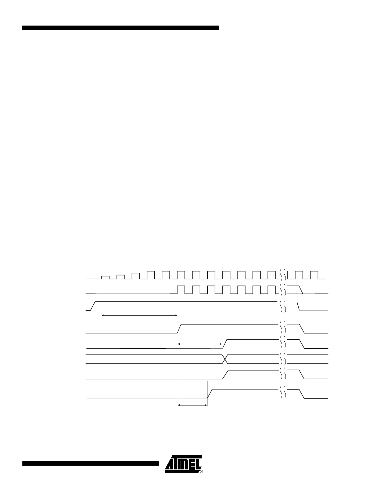
14.3.3 Reset States
14.3.3.1 General Reset
AT91SAM7A3 Preliminary
This feature allows the Reset Controller to shape the NRST pin level, and thus to guarantee
that the NRST line is driven low for a time compliant with potential external devices connected
on the system reset.
As the field is within RSTC_MR, which is backed-up, this field can be used to shape the system power-up reset for devices requiring a longer startup time than the Slow Clock Oscillator.
The Reset State Manager handles the different reset sources and generates the internal reset
signals. It reports the reset status in the field RSTTYP of the Status Register (RSTC_SR). The
update of the field RSTTYP is performed when the processor reset is released.
A general reset occurs when VDDBU is powered on. The backup supply POR cell output rises
and is filtered with a Startup Counter, which operates at Slow Clock. The purpose of this
counter is to make sure the Slow Clock oscillator is stable before starting up the device. The
length of startup time is hardcoded to comply with the Slow Clock Oscillator startup time.
After this time, the processor clock is released at Slow Clock and all the other signals remains
valid for 3 cycles for proper processor and logic reset. Then, all the reset signals are released
and the field RSTTYP in RSTC_SR reports a General Reset. As the RSTC_MR is reset, the
NRST line rises 2 cycles after the backup_nreset, as ERSTL defaults at value 0x0.
When VDDBU is detected low by the Backup Supply POR Cell, all resets signals are immediately asserted, even if the Main Supply POR Cell does not report a Main Supply shut down.
Figure 14-3 shows how the General Reset affects the reset signals.
Figure 14-3. General Reset State
SLCK
MCK
Backup Supply
POR output
backup_nreset
proc_nreset
RSTTYP
periph_nreset
NRST
(nrst_out)
Startup Time
Processor Startup
= 3 cycles
XXX 0x0 = General Reset
Any
Freq.
XXX
6042E–ATARM–14-Dec-06
EXTERNAL RESET LENGTH
= 2 cycles
55
Page 56

14.3.3.2 Wake-up Reset
The Wake-up Reset occurs when the Main Supply is down. When the Main Supply POR output is active, all the reset signals are asserted except backup_nreset. When the Main Supply
powers up, the POR output is resynchronized on Slow Clock. The processor clock is then reenabled during 3 Slow Clock cycles, depending on the requirements of the ARM processor.
At the end of this delay, the processor and other reset signals rise. The field RSTTYP in
RSTC_SR is updated to report a Wake-up Reset.
The “nrst_out” remains asserted for EXTERNAL_RESET_LENGTH cycles. As RSTC_MR is
backed-up, the programmed number of cycles is applicable.
When the Main Supply is detected falling, the reset signals are immediately asserted. This
transition is synchronous with the output of the Main Supply POR.
Figure 14-4. Wake-up State
SLCK
14.3.3.3 User Reset
MCK
Main Supply
POR output
backup_nreset
proc_nreset
RSTTYP
periph_nreset
NRST
(nrst_out)
Resynch.
2 cycles
Processor Startup
= 3 cycles
XXX 0x1 = WakeUp Reset
EXTERNAL RESET LENGTH
= 4 cycles (ERSTL = 1)
Any
Freq.
XXX
The User Reset is entered when a low level is detected on the NRST pin and the bit URSTEN
in RSTC_MR is at 1. The NRST input signal is resynchronized with SLCK to insure proper
behavior of the system.
56
The User Reset is entered as soon as a low level is detected on NRST. The Processor Reset
and the Peripheral Reset are asserted.
The User Reset is left when NRST rises, after a two-cycle resynchronization time and a threecycle processor startup. The processor clock is re-enabled as soon as NRST is confirmed
high.
When the processor reset signal is released, the RSTTYP field of the Status Register
(RSTC_SR) is loaded with the value 0x4, indicating a User Reset.
AT91SAM7A3 Preliminary
6042E–ATARM–14-Dec-06
Page 57

The NRST Manager guarantees that the NRST line is asserted for
EXTERNAL_RESET_LENGTH Slow Clock cycles, as programmed in the field ERSTL. However, if NRST does not rise after EXTERNAL_RESET_LENGTH because it is driven low
externally, the internal reset lines remain asserted until NRST actually rises.
Figure 14-5. User Reset State
SLCK
AT91SAM7A3 Preliminary
MCK
NRST
proc_nreset
RSTTYP
periph_nreset
NRST
(nrst_out)
14.3.3.4 Software Reset
Any
Freq.
Resynch.
2 cycles
Any XXX
>= EXTERNAL RESET LENGTH
Resynch.
2 cycles
Processor Startup
= 3 cycles
0x4 = User Reset
The Reset Controller offers several commands used to assert the different reset signals.
These commands are performed by writing the Control Register (RSTC_CR) with the following
bits at 1:
6042E–ATARM–14-Dec-06
• PROCRST: Writing PROCRST at 1 resets the processor and the watchdog timer.
• PERRST: Writing PERRST at 1 resets all the embedded peripherals, including the memory
system, and, in particular, the Remap Command. The Peripheral Reset is generally used
for debug purposes.
• EXTRST: Writing EXTRST at 1 asserts low the NRST pin during a time defined by the field
ERSTL in the Mode Register (RSTC_MR).
The software reset is entered if at least one of these bits is set by the software. All these commands can be performed independently or simultaneously. The software reset lasts 3 Slow
Clock cycles.
The internal reset signals are asserted as soon as the register write is performed. This is
detected on the Master Clock (MCK). They are released when the software reset is left, i.e.;
synchronously to SLCK.
If EXTRST is set, the nrst_out signal is asserted depending on the programming of the field
ERSTL. However, the resulting falling edge on NRST does not lead to a User Reset.
57
Page 58

If and only if the PROCRST bit is set, the Reset Controller reports the software status in the
field RSTTYP of the Status Register (RSTC_SR). Other Software Resets are not reported in
RSTTYP.
As soon as a software operation is detected, the bit SRCMP (Software Reset Command in
Progress) is set in the Status Register (RSTC_SR). It is cleared as soon as the software reset
is left. No other software reset can be performed while the SRCMP bit is set, and writing any
value in RSTC_CR has no effect.
Figure 14-6. Software Reset
SLCK
14.3.3.5 Watchdog Reset
MCK
Write RSTC_CR
proc_nreset
if PROCRST=1
RSTTYP
periph_nreset
if PERRST=1
NRST
(nrst_out)
if EXTRST=1
SRCMP in RSTC_SR
Any
Freq.
Any
Resynch.
1 cycle
Processor Startup
= 3 cycles
XXX
EXTERNAL RESET LENGTH
0x3 = Software Reset
8 cycles (ERSTL=2)
The Watchdog Reset is entered when a watchdog fault occurs. This state lasts 3 Slow Clock
cycles.
When in Watchdog Reset, assertion of the reset signals depends on the WDRPROC bit in
WDT_MR:
58
• If WDRPROC is 0, the Processor Reset and the Peripheral Reset are asserted. The NRST
line is also asserted, depending on the programming of the field ERSTL. However, the
resulting low level on NRST does not result in a User Reset state.
• If WDRPROC = 1, only the processor reset is asserted.
The Watchdog Timer is reset by the proc_nreset signal. As the watchdog fault always causes
a processor reset if WDRSTEN is set, the Watchdog Timer is always reset after a Watchdog
Reset, and the Watchdog is enabled by default and with a period set to a maximum.
When the WDRSTEN in WDT_MR bit is reset, the watchdog fault has no impact on the reset
controller.
AT91SAM7A3 Preliminary
6042E–ATARM–14-Dec-06
Page 59

Figure 14-7. Watchdog Reset
SLCK
AT91SAM7A3 Preliminary
WDRPROC = 0
14.3.4 Reset State Priorities
The Reset State Manager manages the following priorities between the different reset
sources, given in descending order:
• Backup Reset
• Wake-up Reset
• Watchdog Reset
• Software Reset
• User Reset
Particular cases are listed below:
Only if
MCK
wd_fault
proc_nreset
RSTTYP
periph_nreset
NRST
(nrst_out)
Any
Freq.
Any
Processor Startup
= 3 cycles
XXX
EXTERNAL RESET LENGTH
0x2 = Watchdog Reset
8 cycles (ERSTL=2)
6042E–ATARM–14-Dec-06
• When in User Reset:
– A watchdog event is impossible because the Watchdog Timer is being reset by the
proc_nreset signal.
– A software reset is impossible, since the processor reset is being activated.
• When in Software Reset:
– A watchdog event has priority over the current state.
– The NRST has no effect.
• When in Watchdog Reset:
– The processor reset is active and so a Software Reset cannot be programmed.
– A User Reset cannot be entered.
59
Page 60

14.3.5 Reset Controller Status Register
The Reset Controller status register (RSTC_SR) provides several status fields:
• RSTTYP field: This field gives the type of the last reset, as explained in previous sections.
• SRCMP bit: This field indicates that a Software Reset Command is in progress and that no
further software reset should be performed until the end of the current one. This bit is
automatically cleared at the end of the current software reset.
• NRSTL bit: The NRSTL bit of the Status Register gives the level of the NRST pin sampled
on each MCK rising edge.
• URSTS bit: A high-to-low transition of the NRST pin sets the URSTS bit of the RSTC_SR
register. This transition is also detected on the Master Clock (MCK) rising edge (see Figure
14-8). If the User Reset is disabled (URSTEN = 0) and if the interruption is enabled by the
URSTIEN bit in the RSTC_MR register, the URSTS bit triggers an interrupt. Reading the
RSTC_SR status register resets the URSTS bit and clears the interrupt.
Figure 14-8. Reset Controller Status and Interrupt
MCK
Peripheral Access
NRST
NRSTL
URSTS
rstc_irq
if (URSTEN = 0) and
(URSTIEN = 1)
2 cycle
resynchronization
read
RSTC_SR
2 cycle
resynchronization
60
AT91SAM7A3 Preliminary
6042E–ATARM–14-Dec-06
Page 61

AT91SAM7A3 Preliminary
14.4 Reset Controller (RSTC) User Interface
Table 14-1. Reset Controller (RSTC) Register Mapping
Back-up Reset
Offset Register Name Access Reset Value
0x00 Control Register RSTC_CR Write-only -
0x04 Status Register RSTC_SR Read-only 0x0000_0001 0x0000_0000
0x08 Mode Register RSTC_MR Read/Write - 0x0000_0000
Note: 1. The reset value of RSTC_SR either reports a General Reset or a Wake-up Reset depending on last rising power supply.
Value
6042E–ATARM–14-Dec-06
61
Page 62

14.4.1 Reset Controller Control Register Register Name: RSTC_CR
Access Type: Write-only
31 30 29 28 27 26 25 24
KEY
23 22 21 20 19 18 17 16
––––––––
15 14 13 12 11 10 9 8
–––––– –
76543210
––––EXTRSTPERRST–PROCRST
• PROCRST: Processor Reset
0 = No effect.
1 = If KEY is correct, resets the processor.
• PERRST: Peripheral Reset
0 = No effect.
1 = If KEY is correct, resets the peripherals.
• EXTRST: External Reset
0 = No effect.
1 = If KEY is correct, asserts the NRST pin.
•KEY: Password
Should be written at value 0xA5. Writing any other value in this field aborts the write operation.
62
AT91SAM7A3 Preliminary
6042E–ATARM–14-Dec-06
Page 63

AT91SAM7A3 Preliminary
14.4.2 Reset Controller Status Register Register Name: RSTC_SR
Access Type: Read-only
31 30 29 28 27 26 25 24
––––––––
23 22 21 20 19 18 17 16
––––––SRCMPNRSTL
15 14 13 12 11 10 9 8
––––– RSTTYP
76543210
–––––– URSTS
• URSTS: User Reset Status
0 = No high-to-low edge on NRST happened since the last read of RSTC_SR.
1 = At least one high-to-low transition of NRST has been detected since the last read of RSTC_SR.
• RSTTYP: Reset Type
Reports the cause of the last processor reset. Reading this RSTC_SR does not reset this field.
RSTTYP Reset Type Comments
0 0 0 General Reset Both VDD1V8 and VDDBU rising
0 0 1 Wake Up Reset VDD1V8 rising
0 1 0 Watchdog Reset Watchdog fault occurred
0 1 1 Software Reset Processor reset required by the software
1 0 0 User Reset NRST pin detected low
• NRSTL: NRST Pin Level
Registers the NRST Pin Level at Master Clock (MCK).
• SRCMP: Software Reset Command in Progress
0 = No software command is being performed by the reset controller. The reset controller is ready for a software command.
1 = A software reset command is being performed by the reset controller. The reset controller is busy.
6042E–ATARM–14-Dec-06
63
Page 64

14.4.3 Reset Controller Mode Register Register Name: RSTC_MR
Access Type: Read/Write
31 30 29 28 27 26 25 24
KEY
23 22 21 20 19 18 17 16
–––––––
15 14 13 12 11 10 9 8
–––– ERSTL
76543210
– – URSTIEN – – – URSTEN
• URSTEN: User Reset Enable
0 = The detection of a low level on the pin NRST does not generate a User Reset.
1 = The detection of a low level on the pin NRST triggers a User Reset.
• URSTIEN: User Reset Interrupt Enable
0 = USRTS bit in RSTC_SR at 1 has no effect on rstc_irq.
1 = USRTS bit in RSTC_SR at 1 asserts rstc_irq if URSTEN = 0.
• ERSTL: External Reset Length
This field defines the external reset length. The external reset is asserted during a time of 2
(ERSTL+1)
allows assertion duration to be programmed between 60 µs and 2 seconds.
•KEY: Password
Should be written at value 0xA5. Writing any other value in this field aborts the write operation.
Slow Clock cycles. This
64
AT91SAM7A3 Preliminary
6042E–ATARM–14-Dec-06
Page 65

15. Real-time Timer (RTT)
15.1 Overview
The Real-time Timer is built around a 32-bit counter and used to count elapsed seconds. It generates a periodic interrupt or/and triggers an alarm on a programmed value.
15.2 Block Diagram
Figure 15-1. Real-time Timer
AT91SAM7A3 Preliminary
SLCK
RTT_MR
RTTRST
reload
16-bit
Divider
RTT_MR
RTPRES
RTT_MR
RTTRST
RTT_VR
RTT_AR
0
10
32-bit
Counter
CRTV
ALMV
RTT_SR
RTT_SR
RTT_SR
=
read
set
reset
reset
set
RTT_MR
RTTINCIEN
RTTINC
rtt_int
RTT_MR
ALMIEN
ALMS
rtt_alarm
15.3 Functional Description
The Real-time Timer is used to count elapsed seconds. It is built around a 32-bit counter fed by
Slow Clock divided by a programmable 16-bit value. The value can be programmed in the field
RTPRES of the Real-time Mode Register (RTT_MR).
Programming RTPRES at 0x00008000 corresponds to feeding the real-time counter with a 1 Hz
signal (if the Slow Clock is 32.768 Hz). The 32-bit counter can count up to 2
sponding to more than 136 years, then roll over to 0.
The Real-time Timer can also be used as a free-running timer with a lower time-base. The best
accuracy is achieved by writing RTPRES to 3. Programming RTPRES to 1 or 2 is possible, but
may result in losing status events because the status register is cleared two Slow Clock cycles
after read. Thus if the RTT is configured to trigger an interrupt, the interrupt occurs during 2 Slow
Clock cycles after reading RTT_SR. To prevent several executions of the interrupt handler, the
interrupt must be disabled in the interrupt handler and re-enabled when the status register is
clear.
6042E–ATARM–14-Dec-06
32
seconds, corre-
65
Page 66

The Real-time Timer value (CRTV) can be read at any time in the register RTT_VR (Real-time
Value Register). As this value can be updated asynchronously from the Master Clock, it is advisable to read this register twice at the same value to improve accuracy of the returned value.
The current value of the counter is compared with the value written in the alarm register
RTT_AR (Real-time Alarm Register). If the counter value matches the alarm, the bit ALMS in
RTT_SR is set. The alarm register is set to its maximum value, corresponding to 0xFFFF_FFFF,
after a reset.
The bit RTTINC in RTT_SR is set each time the Real-time Timer counter is incremented. This bit
can be used to start a periodic interrupt, the period being one second when the RTPRES is programmed with 0x8000 and Slow Clock equal to 32.768 Hz.
Reading the RTT_SR status register resets the RTTINC and ALMS fields.
Writing the bit RTTRST in RTT_MR immediately reloads and restarts the clock divider with the
new programmed value. This also resets the 32-bit counter.
Note: Because of the asynchronism between the Slow Clock (SCLK) and the System Clock (MCK):
1) The restart of the counter and the reset of the RTT_VR current value register is effective only 2
slow clock cycles after the write of the RTTRST bit in the RTT_MR register.
2) The status register flags reset is taken into account only 2 slow clock cycles after the read of the
RTT_SR (Status Register).
Figure 15-2. RTT Counting
MCK
RTPRES - 1
Prescaler
RTT
RTTINC (RTT_SR)
ALMS (RTT_SR)
APB Interface
APB cycle
0
...
ALMVALMV-10 ALMV+1
read RTT_SR
ALMV+2 ALMV+3
APB cycle
66
AT91SAM7A3 Preliminary
6042E–ATARM–14-Dec-06
Page 67

AT91SAM7A3 Preliminary
15.4 Real-time Timer (RTT) User Interface
Table 15-1. Real-time Timer (RTT) Register Mapping
Offset Register Name Access Reset Value
0x00 Mode Register RTT_MR Read/Write 0x0000_8000
0x04 Alarm Register RTT_AR Read/Write 0xFFFF_FFFF
0x08 Value Register RTT_VR Read-only 0x0000_0000
0x0C Status Register RTT_SR Read-only 0x0000_0000
6042E–ATARM–14-Dec-06
67
Page 68

15.4.1 Real-time Timer Mode Register Register Name: RTT_MR
Access Type: Read/Write
31 30 29 28 27 26 25 24
––––––––
23 22 21 20 19 18 17 16
–––––RTTRSTRTTINCIENALMIEN
15 14 13 12 11 10 9 8
RTPRES
76543210
RTPRES
• RTPRES: Real-time Timer Prescaler Value
Defines the number of SLCK periods required to increment the real-time timer. RTPRES is defined as follows:
RTPRES = 0: The Prescaler Period is equal to 2
16
RTPRES ≠ 0: The Prescaler Period is equal to RTPRES.
• ALMIEN: Alarm Interrupt Enable
0 = The bit ALMS in RTT_SR has no effect on interrupt.
1 = The bit ALMS in RTT_SR asserts interrupt.
• RTTINCIEN: Real-time Timer Increment Interrupt Enable
0 = The bit RTTINC in RTT_SR has no effect on interrupt.
1 = The bit RTTINC in RTT_SR asserts interrupt.
• RTTRST: Real-time Timer Restart
1 = Reloads and restarts the clock divider with the new programmed value. This also resets the 32-bit counter.
68
AT91SAM7A3 Preliminary
6042E–ATARM–14-Dec-06
Page 69

AT91SAM7A3 Preliminary
15.4.2 Real-time Timer Alarm Register Register Name: RTT_AR
Access Type: Read/Write
31 30 29 28 27 26 25 24
ALMV
23 22 21 20 19 18 17 16
ALMV
15 14 13 12 11 10 9 8
ALMV
76543210
ALMV
• ALMV: Alarm Value
Defines the alarm value (ALMV+1) compared with the Real-time Timer.
15.4.3 Real-time Timer Value Register Register Name: RTT_VR
Access Type: Read-only
31 30 29 28 27 26 25 24
CRTV
23 22 21 20 19 18 17 16
CRTV
15 14 13 12 11 10 9 8
CRTV
76543210
CRTV
• CRTV: Current Real-time Value
Returns the current value of the Real-time Timer.
6042E–ATARM–14-Dec-06
69
Page 70

15.4.4 Real-time Timer Status Register Register Name: RTT_SR
Access Type: Read-only
31 30 29 28 27 26 25 24
––––––––
23 22 21 20 19 18 17 16
––––––––
15 14 13 12 11 10 9 8
––––––––
76543210
––––––RTTINCALMS
• ALMS: Real-time Alarm Status
0 = The Real-time Alarm has not occurred since the last read of RTT_SR.
1 = The Real-time Alarm occurred since the last read of RTT_SR.
• RTTINC: Real-time Timer Increment
0 = The Real-time Timer has not been incremented since the last read of the RTT_SR.
1 = The Real-time Timer has been incremented since the last read of the RTT_SR.
70
AT91SAM7A3 Preliminary
6042E–ATARM–14-Dec-06
Page 71

16. Periodic Interval Timer (PIT)
16.1 Overview
The Periodic Interval Timer (PIT) provides the operating system’s scheduler interrupt. It is
designed to offer maximum accuracy and efficient management, even for systems with long
response time.
16.2 Block Diagram
Figure 16-1. Periodic Interval Timer
AT91SAM7A3 Preliminary
PIT_MR
PIV
0
MCK
Prescaler
MCK/16
20-bit
Counter
CPIV
CPIV PICNT
16.3 Functional Description
The Periodic Interval Timer aims at providing periodic interrupts for use by operating systems.
= ?
set
0
0
1
PIT_PIVR
PIT_PIIR
10
12-bit
Adder
PICNT
PIT_SR
PITS
reset
read PIT_PIVR
PIT_MR
PITIEN
pit_irq
6042E–ATARM–14-Dec-06
The PIT provides a programmable overflow counter and a reset-on-read feature. It is built
around two counters: a 20-bit CPIV counter and a 12-bit PICNT counter. Both counters work
at Master Clock /16.
The first 20-bit CPIV counter increments from 0 up to a programmable overflow value set in
the field PIV of the Mode Register (PIT_MR). When the counter CPIV reaches this value, it
resets to 0 and increments the Periodic Interval Counter, PICNT. The status bit PITS in the
Status Register (PIT_SR) rises and triggers an interrupt, provided the interrupt is enabled
(PITIEN in PIT_MR).
Writing a new PIV value in PIT_MR does not reset/restart the counters.
71
Page 72

When CPIV and PICNT values are obtained by reading the Periodic Interval Value Register
(PIT_PIVR), the overflow counter (PICNT) is reset and the PITS is cleared, thus acknowledging the interrupt. The value of PICNT gives the number of periodic intervals elapsed since the
last read of PIT_PIVR.
When CPIV and PICNT values are obtained by reading the Periodic Interval Image Register
(PIT_PIIR), there is no effect on the counters CPIV and PICNT, nor on the bit PITS. For example, a profiler can read PIT_PIIR without clearing any pending interrupt, whereas a timer
interrupt clears the interrupt by reading PIT_PIVR.
The PIT may be enabled/disabled using the PITEN bit in the PIT_MR register (disabled on
reset). The PITEN bit only becomes effective when the CPIV value is 0. Figure 16-2 illustrates
the PIT counting. After the PIT Enable bit is reset (PITEN= 0), the CPIV goes on counting until
the PIV value is reached, and is then reset. PIT restarts counting, only if the PITEN is set
again.
The PIT is stopped when the core enters debug state.
Figure 16-2. Enabling/Disabling PIT with PITEN
MCK
APB cycle
APB cycle
MCK Prescaler
PITEN
CPIV
PICNT
PITS (PIT_SR)
APB Interface
15
restarts MCK Prescaler
0
10
0
PIVPIV - 10
1
read PIT_PIVR
0
1
72
AT91SAM7A3 Preliminary
6042E–ATARM–14-Dec-06
Page 73

AT91SAM7A3 Preliminary
16.4 Periodic Interval Timer (PIT) User Interface
Table 16-1. Periodic Interval Timer (PIT) Register Mapping
Offset Register Name Access Reset Value
0x00 Mode Register PIT_MR Read/Write 0x000F_FFFF
0x04 Status Register PIT_SR Read-only 0x0000_0000
0x08 Periodic Interval Value Register PIT_PIVR Read-only 0x0000_0000
0x0C Periodic Interval Image Register PIT_PIIR Read-only 0x0000_0000
16.4.1 Periodic Interval Timer Mode Register Register Name: PIT_MR
Access Type: Read/Write
31 30 29 28 27 26 25 24
––––––PITIENPITEN
23 22 21 20 19 18 17 16
–––– PIV
15 14 13 12 11 10 9 8
PIV
76543210
PIV
• PIV: Periodic Interval Value
Defines the value compared with the primary 20-bit counter of the Periodic Interval Timer (CPIV). The period is equal to
(PIV + 1).
• PITEN: Period Interval Timer Enabled
0 = The Periodic Interval Timer is disabled when the PIV value is reached.
1 = The Periodic Interval Timer is enabled.
• PITIEN: Periodic Interval Timer Interrupt Enable
0 = The bit PITS in PIT_SR has no effect on interrupt.
1 = The bit PITS in PIT_SR asserts interrupt.
6042E–ATARM–14-Dec-06
73
Page 74

16.4.2 Periodic Interval Timer Status Register Register Name: PIT_SR
Access Type: Read-only
31 30 29 28 27 26 25 24
––––––––
23 22 21 20 19 18 17 16
––––––––
15 14 13 12 11 10 9 8
––––––––
76543210
–––––––PITS
• PITS: Periodic Interval Timer Status
0 = The Periodic Interval timer has not reached PIV since the last read of PIT_PIVR.
1 = The Periodic Interval timer has reached PIV since the last read of PIT_PIVR.
74
AT91SAM7A3 Preliminary
6042E–ATARM–14-Dec-06
Page 75

AT91SAM7A3 Preliminary
16.4.3 Periodic Interval Timer Value Register Register Name: PIT_PIVR
Access Type: Read-only
31 30 29 28 27 26 25 24
PICNT
23 22 21 20 19 18 17 16
PICNT CPIV
15 14 13 12 11 10 9 8
CPIV
76543210
CPIV
Reading this register clears PITS in PIT_SR.
• CPIV: Current Periodic Interval Value
Returns the current value of the periodic interval timer.
• PICNT: Periodic Interval Counter
Returns the number of occurrences of periodic intervals since the last read of PIT_PIVR.
6042E–ATARM–14-Dec-06
75
Page 76

16.4.4 Periodic Interval Timer Image Register Register Name: PIT_PIIR
Access Type: Read-only
31 30 29 28 27 26 25 24
PICNT
23 22 21 20 19 18 17 16
PICNT CPIV
15 14 13 12 11 10 9 8
CPIV
76543210
CPIV
• CPIV: Current Periodic Interval Value
Returns the current value of the periodic interval timer.
• PICNT: Periodic Interval Counter
Returns the number of occurrences of periodic intervals since the last read of PIT_PIVR.
76
AT91SAM7A3 Preliminary
6042E–ATARM–14-Dec-06
Page 77

17. Watchdog Timer (WDT)
17.1 Overview
The Watchdog Timer can be used to prevent system lock-up if the software becomes trapped in
a deadlock. It features a 12-bit down counter that allows a watchdog period of up to 16 seconds
(slow clock at 32.768 kHz). It can generate a general reset or a processor reset only. In addition,
it can be stopped while the processor is in debug mode or idle mode.
17.2 Block Diagram
Figure 17-1. Watchdog Timer Block Diagram
AT91SAM7A3 Preliminary
WDT_CR
WDRSTT
read WDT_SR
or
reset
write WDT_MR
WDT_MR
WDD
<= WDD
WDERR
set
reset
reload
WDT_MR
WDV
10
12-bit Down
Counter
Current
Value
WDUNF
=
reset
0
set
reload
1/128
SLCK
WDT_MR
WDRSTEN
wdt_fault
(to Reset Controller)
wdt_int
WDFIEN
WDT_MR
6042E–ATARM–14-Dec-06
77
Page 78

17.3 Functional Description
The Watchdog Timer can be used to prevent system lock-up if the software becomes trapped in
a deadlock. It is supplied with VDDCORE. It restarts with initial values on processor reset.
The Watchdog is built around a 12-bit down counter, which is loaded with the value defined in
the field WDV of the Mode Register (WDT_MR). The Watchdog Timer uses the Slow Clock
divided by 128 to establish the maximum Watchdog period to be 16 seconds (with a typical Slow
Clock of 32.768 kHz).
After a Processor Reset, the value of WDV is 0xFFF, corresponding to the maximum value of
the counter with the external reset generation enabled (field WDRSTEN at 1 after a Backup
Reset). This means that a default Watchdog is running at reset, i.e., at power-up. The user must
either disable it (by setting the WDDIS bit in WDT_MR) if he does not expect to use it or must
reprogram it to meet the maximum Watchdog period the application requires.
The Watchdog Mode Register (WDT_MR) can be written only once. Only a processor reset
resets it. Writing the WDT_MR register reloads the timer with the newly programmed mode
parameters.
In normal operation, the user reloads the Watchdog at regular intervals before the timer underflow occurs, by writing the Control Register (WDT_CR) with the bit WDRSTT to 1. The
Watchdog counter is then immediately reloaded from WDT_MR and restarted, and the Slow
Clock 128 divider is reset and restarted. The WDT_CR register is write-protected. As a result,
writing WDT_CR without the correct hard-coded key has no effect. If an underflow does occur,
the “wdt_fault” signal to the Reset Controller is asserted if the bit WDRSTEN is set in the Mode
Register (WDT_MR). Moreover, the bit WDUNF is set in the Watchdog Status Register
(WDT_SR).
To prevent a software deadlock that continuously triggers the Watchdog, the reload of the
Watchdog must occur while the Watchdog counter is within a window between 0 and WDD,
WDD is defined in the WatchDog Mode Register WDT_MR.
Any attempt to restart the Watchdog while the Watchdog counter is between WDV and WDD
results in a Watchdog error, even if the Watchdog is disabled. The bit WDERR is updated in the
WDT_SR and the “wdt_fault” signal to the Reset Controller is asserted.
Note that this feature can be disabled by programming a WDD value greater than or equal to the
WDV value. In such a configuration, restarting the Watchdog Timer is permitted in the whole
range [0; WDV] and does not generate an error. This is the default configuration on reset (the
WDD and WDV values are equal).
The status bits WDUNF (Watchdog Underflow) and WDERR (Watchdog Error) trigger an interrupt, provided the bit WDFIEN is set in the mode register. The signal “wdt_fault” to the reset
controller causes a Watchdog reset if the WDRSTEN bit is set as already explained in the reset
controller programmer Datasheet. In that case, the processor and the Watchdog Timer are
reset, and the WDERR and WDUNF flags are reset.
If a reset is generated or if WDT_SR is read, the status bits are reset, the interrupt is cleared,
and the “wdt_fault” signal to the reset controller is deasserted.
Writing the WDT_MR reloads and restarts the down counter.
While the processor is in debug state or in idle mode, the counter may be stopped depending on
the value programmed for the bits WDIDLEHLT and WDDBGHLT in the WDT_MR.
78
AT91SAM7A3 Preliminary
6042E–ATARM–14-Dec-06
Page 79

Figure 17-2. Watchdog Behavior
AT91SAM7A3 Preliminary
Watchdog Error
Watchdog Underflow
FFF
WDV
Forbidden
Window
WDD
Permitted
Window
0
Watchdog
Fault
Normal behavior
if WDRSTEN is 1
if WDRSTEN is 0
WDT_CR = WDRSTT
6042E–ATARM–14-Dec-06
79
Page 80

17.4 Watchdog Timer (WDT) User Interface
Table 17-1. Watchdog Timer (WDT) Register Mapping
Offset Register Name Access Reset Value
0x00 Control Register WDT_CR Write-only -
0x04 Mode Register WDT_MR Read/Write Once 0x3FFF_2FFF
0x08 Status Register WDT_SR Read-only 0x0000_0000
17.4.1 Watchdog Timer Control Register Register Name: WDT_CR Access Type: Write-only
31 30 29 28 27 26 25 24
23 22 21 20 19 18 17 16
––––––––
15 14 13 12 11 10 9 8
––––––––
KEY
76543210
–––––––WDRSTT
• WDRSTT: Watchdog Restart
0: No effect.
1: Restarts the Watchdog.
•KEY: Password
Should be written at value 0xA5. Writing any other value in this field aborts the write operation.
80
AT91SAM7A3 Preliminary
6042E–ATARM–14-Dec-06
Page 81

AT91SAM7A3 Preliminary
17.4.2 Watchdog Timer Mode Register Register Name: WDT_MR Access Type: Read/Write Once
31 30 29 28 27 26 25 24
– – WDIDLEHLT WDDBGHLT WDD
23 22 21 20 19 18 17 16
WDD
15 14 13 12 11 10 9 8
WDDIS
76543210
• WDV: Watchdog Counter Value
Defines the value loaded in the 12-bit Watchdog Counter.
• WDFIEN: Watchdog Fault Interrupt Enable
0: A Watchdog fault (underflow or error) has no effect on interrupt.
1: A Watchdog fault (underflow or error) asserts interrupt.
WDRPROC WDRSTEN WDFIEN WDV
WDV
• WDRSTEN: Watchdog Reset Enable
0: A Watchdog fault (underflow or error) has no effect on the resets.
1: A Watchdog fault (underflow or error) triggers a Watchdog reset.
• WDRPROC: Watchdog Reset Processor
0: If WDRSTEN is 1, a Watchdog fault (underflow or error) activates all resets.
1: If WDRSTEN is 1, a Watchdog fault (underflow or error) activates the processor reset.
• WDD: Watchdog Delta Value
Defines the permitted range for reloading the Watchdog Timer.
If the Watchdog Timer value is less than or equal to WDD, writing WDT_CR with WDRSTT = 1 restarts the timer.
If the Watchdog Timer value is greater than WDD, writing WDT_CR with WDRSTT = 1 causes a Watchdog error.
• WDDBGHLT: Watchdog Debug Halt
0: The Watchdog runs when the processor is in debug state.
1: The Watchdog stops when the processor is in debug state.
• WDIDLEHLT: Watchdog Idle Halt
0: The Watchdog runs when the system is in idle mode.
1: The Watchdog stops when the system is in idle state.
• WDDIS: Watchdog Disable
0: Enables the Watchdog Timer.
1: Disables the Watchdog Timer.
6042E–ATARM–14-Dec-06
81
Page 82

17.4.3 Watchdog Timer Status Register Register Name: WDT_SR Access Type: Read-only
31 30 29 28 27 26 25 24
––––––––
23 22 21 20 19 18 17 16
––––––––
15 14 13 12 11 10 9 8
––––––––
76543210
––––––WDERRWDUNF
• WDUNF: Watchdog Underflow
0: No Watchdog underflow occurred since the last read of WDT_SR.
1: At least one Watchdog underflow occurred since the last read of WDT_SR.
• WDERR: Watchdog Error
0: No Watchdog error occurred since the last read of WDT_SR.
1: At least one Watchdog error occurred since the last read of WDT_SR.
82
AT91SAM7A3 Preliminary
6042E–ATARM–14-Dec-06
Page 83

18. Shutdown Controller (SHDWC)
18.1 Overview
The Shutdown Controller controls the power supplies VDD3V3 and VDD1V8 and the wake-up
detection on debounced input lines. A dedicated input, Force Wake Up, is also available.
18.2 Block Diagram
Figure 18-1. Shutdown Controller Block Diagram
Shutdown Controller
SYSC_SHMR
CPTWK0
WKMODE0
WKUP0
Detector
WKUP1
CPTWK1
WKMODE1
Event0
Event
Event1
read SYSC_SHSR
reset
WAKEUP0
set
read SYSC_SHSR
reset
WAKEUP1
set
AT91SAM7A3 Preliminary
SLCK
SYSC_SHSR
SYSC_SHSR
RTT Alarm
RTTWKEN
SYSC_SHMR
read SYSC_SHSR
reset
RTTWK
set
SYSC_SHSR
FWKUP
SYSC_SHCR
SHDW
read SYSC_SHSR
reset
FWKUP
set
SYSC_SHSR
Wake-up
Shutdown
Output
Controller
Shutdown
SHDW
6042E–ATARM–14-Dec-06
83
Page 84

18.3 I/O Lines Description
Table 18-1. I/O Lines Description
Name Description Type
FWKUP
WKUP0
WKUP1
SHDW
18.4 Product Dependencies
18.4.1 Power Management
The Shutdown Controller is continuously clocked by Slow Clock. The Power Management
Controller has no effect on the behavior of the Shutdown Controller.
18.5 Functional Description
The Shutdown Controller manages the main power supply. To do so, it is supplied with
VDDBU and manages wake-up input pins and one output pin, SHDW.
A typical application connects the pin SHDW to the shutdown input of the DC/DC Converter
providing the main power supplies of the system, and especially VDD1V8 and/or VDD3V3.
The wake-up inputs (WKUP0, WKUP1, FWKUP) connect to any push-buttons or signal that
wake up the system.
Force Wake Up input for the Shutdown Controller
Wake-up 0 input
Wake-up 1input
Shutdown output
Input
Input
Input
Output
The software is able to control the pin SHDW by writing the Shutdown Control Register
(SHDW_CR) with the bit SHDW at 1. This register is password-protected and so the value
written should contain the correct key for the command to be taken into account. As a result,
the system should be powered down.
A level change on WKUP0 or WKUP1 is used as wake-up. Wake-up is configured in the Shutdown Mode Register (SHDW_MR). The transition detector can be programmed to detect
either a positive or negative transition or any level change on WKUP0 and WKUP1. The
detection can also be disabled. Programming is performed by defining WKMODE0 and
WKMODE1.
Moreover, a debouncing circuit can be programmed for WKUP0 or WKUP1. The debouncing
circuit filters pulses on WKUP0 or WKUP1 shorter than the programmed number of 16 SLCK
cycles in CPTWK0 or CPTWK1 of the SHDW_MR register. If the programmed level change is
detected on a pin, a counter starts. When the counter reaches the value programmed in the
corresponding field, CPTWK0 or CPTWK1, the SHDW pin is released. If a new input change
is detected before the counter reaches the corresponding value, the counter is stopped and
cleared. WAKEUP0 and/or WAKEUP1 of the Status Register (SHDW_SR) reports the detection of the programmed events on WKUP0 or WKUP1, with a reset after the read of
SHDW_SR.
The Shutdown Controller can be programmed so as to activate the wake-up using the RTT
alarm (the detection of the rising edge of the RTT alarm is synchronized with SLCK). This is
done by writing the SHDW_MR register using the RTTWKEN fields. When enabled, the detection of the RTT alarm is reported in the RTTWK bit of the SHDW_SR Status register. It is reset
84
AT91SAM7A3 Preliminary
6042E–ATARM–14-Dec-06
Page 85

AT91SAM7A3 Preliminary
after the read of SHDW_SR. When using the RTT alarm to wake up the system, the user must
ensure that the RTT alarm status flag is cleared before shutting down the system. Otherwise,
no rising edge of the status flag may be detected and the wake-up fails.
The pin FWKUP is treated differently and a low level on this pin forces a de-assertion of the
SHDW pin, regardless of the presence of the Slow Clock. The bit FWKUP in the status register
reports a Forced Wakeup Event after internal resynchronization of the event with the Slow
Clock.
6042E–ATARM–14-Dec-06
85
Page 86

18.6 Shutdown Controller (SHDWC) User Interface
18.6.1 Register Mapping
Table 18-2. Shutdown Controller (SHDWC) Registers
Offset Register Name Access Reset Value
0x00 Shutdown Control Register SHDW_CR Write-only -
0x04 Shutdown Mode Register SHDW_MR Read-Write 0x0000_0303
0x18 Shutdown Status Register SHDW_SR Read-only 0x0000_0000
18.6.2 Shutdown Control Register Register Name: SHDW_CR Access Type: Write-only
31 30 29 28 27 26 25 24
KEY
23 22 21 20 19 18 17 16
––––––––
15 14 13 12 11 10 9 8
––––––––
76543210
–––––––SHDW
• SHDW: Shut Down Command
0 = No effect.
1 = If KEY is correct, asserts the SHDW pin.
•KEY: Password
Should be written at value 0xA5. Writing any other value in this field aborts the write operation.
86
AT91SAM7A3 Preliminary
6042E–ATARM–14-Dec-06
Page 87
AT91SAM7A3 Preliminary
18.6.3 Shutdown Mode Register Register Name: SHDW_MR Access Type: Read/Write
31 30 29 28 27 26 25 24
––––––––
23 22 21 20 19 18 17 16
–––––––RTTWKEN
15 14 13 12 11 10 9 8
CPTWK1 – – WKMODE1
76543210
CPTWK0 – – WKMODE0
• WKMODE0: Wake-up Mode 0
• WKMODE1: Wake-up Mode 1
WKMODE[1:0] Wake-up Input Transition Selection
0 0 None. No detection is performed on the wake-up input
0 1 Low to high level
1 0 High to low level
1 1 Both levels change
• CPTWK0: Counter on Wake-up 0
• CPTWK1: Counter on Wake-up 1
Defines the number of 16 Slow Clock cycles, the level detection on the corresponding input pin shall last before the wakeup event occurs. Because of the internal synchronization of WKUP0 and WKUP1, the SHDW pin is released
(CPTWK x 16 + 1) Slow Clock cycles after the event on WKUP.
• RTTWKEN: Real-time Timer Wake-up Enable
0 = The RTT Alarm signal has no effect on the Shutdown Controller.
1 = The RTT Alarm signal forces the de-assertion of the SHDW pin.
6042E–ATARM–14-Dec-06
87
Page 88

18.6.4 Shutdown Status Register Register Name: SHDW_SR Access Type: Read-only
31 30 29 28 27 26 25 24
––––––––
23 22 21 20 19 18 17 16
–––––––RTTWK
15 14 13 12 11 10 9 8
––––––––
76543210
–––––FWKUPWAKEUP1 WAKEUP0
• WAKEUP0: Wake-up 0 Status
• WAKEUP1: Wake-up 1 Status
0 = No wake-up event occurred on the corresponding wake-up input since the last read of SHDW_SR.
1 = At least one wake-up event occurred on the corresponding wake-up input since the last read of SHDW_SR.
• FWKUP: Force Wake Up Status
0 = No wake-up event occurred on the Force Wake Up input since the last read of SHDW_SR.
1 = At least one wake-up event occurred on the Force Wake Up input since the last read of SHDW_SR.
• RTTWK: Real-time Timer Wake-up
0 = No wake-up alarm from the RTT occurred since the last read of SHDW_SR.
1 = At least one wake-up alarm from the RTT occurred since the last read of SHDW_SR.
88
AT91SAM7A3 Preliminary
6042E–ATARM–14-Dec-06
Page 89

19. Memory Controller (MC)
19.1 Overview
The Memory Controller (MC) manages the ASB bus and controls accesses requested by the
masters, typically the ARM7TDMI processor and the Peripheral Data Controller. It features a
simple bus arbiter, an address decoder, an abort status, a misalignment detector and an
Embedded Flash Controller. In addition, the MC contains a Memory Protection Unit (MPU)
consisting of 16 areas that can be protected against write and/or user accesses. Access to
peripherals can be protected in the same way.
19.2 Block Diagram
Figure 19-1. Memory Controller Block Diagram
Memory Controller
AT91SAM7A3 Preliminary
ASB
ARM7TDMI
Processor
Peripheral
Data
Controller
Abort
Bus
Arbiter
Abort
Status
Misalignment
Detector
Memory
Protection
Unit
User
Interface
Decoder
APB
Bridge
Embedded
Flash
Controller
Address
Internal
Flash
Internal
RAM
6042E–ATARM–14-Dec-06
Peripheral 0
Peripheral 1
Peripheral N
APB
From Master
to Slave
89
Page 90

19.3 Functional Description
The Memory Controller handles the internal ASB bus and arbitrates the accesses of both
masters.
It is made up of:
• A bus arbiter
• An address decoder
• An abort status
• A misalignment detector
• A memory protection unit
• An Embedded Flash Controller
The MC handles only little-endian mode accesses. The masters work in little-endian mode
only.
19.3.1 Bus Arbiter
The Memory Controller has a simple, hard-wired priority bus arbiter that gives the control of
the bus to one of the two masters. The Peripheral Data Controller has the highest priority; the
ARM processor has the lowest one.
19.3.2 Address Decoder
The Memory Controller features an Address Decoder that first decodes the four highest bits of
the 32-bit address bus and defines three separate areas:
• One 256-Mbyte address space for the internal memories
• One 256-Mbyte address space reserved for the embedded peripherals
• An undefined address space of 3584M bytes representing fourteen 256-Mbyte areas that
return an Abort if accessed
Figure 19-2 shows the assignment of the 256-Mbyte memory areas.
Figure 19-2. Memory Areas
256M Bytes
14 x 256MBytes
3,584 Mbytes
256M Bytes
0x0000 0000
0x0FFF FFFF
0x1000 0000
0xEFFF FFFF
0xF000 0000
0xFFFF FFFF
Internal Memories
Undefined
(Abort)
Peripherals
90
AT91SAM7A3 Preliminary
6042E–ATARM–14-Dec-06
Page 91

19.3.2.1 Internal Memory Mapping
Within the Internal Memory address space, the Address Decoder of the Memory Controller
decodes eight more address bits to allocate 1-Mbyte address spaces for the embedded
memories.
The allocated memories are accessed all along the 1-Mbyte address space and so are
repeated n times within this address space, n equaling 1M bytes divided by the size of the
memory.
When the address of the access is undefined within the internal memory area, the Address
Decoder returns an Abort to the master.
Figure 19-3. Internal Memory Mapping
256M Bytes
0x0000 0000
0x000F FFFF
0x0010 0000
0x001F FFFF
0x0020 0000
0x002F FFFF
0x0030 0000
AT91SAM7A3 Preliminary
Internal Memory Area 0
Internal Memory Area 1
Internal Flash
Internal Memory Area 2
Internal SRAM
1M Bytes
1M Bytes
1M Bytes
19.3.2.2 Internal Memory Area 0
The first 32 bytes of Internal Memory Area 0 contain the ARM processor exception vectors, in
particular, the Reset Vector at address 0x0.
Before execution of the remap command, the on-chip Flash is mapped into Internal Memory
Area 0, so that the ARM7TDMI reaches an executable instruction contained in Flash. After the
remap command, the internal SRAM at address 0x0020 0000 is mapped into Internal Memory
Area 0. The memory mapped into Internal Memory Area 0 is accessible in both its original
location and at address 0x0.
19.3.3 Remap Command
After execution, the Remap Command causes the Internal SRAM to be accessed through the
Internal Memory Area 0.
As the ARM vectors (Reset, Abort, Data Abort, Prefetch Abort, Undefined Instruction, Interrupt, and Fast Interrupt) are mapped from address 0x0 to address 0x20, the Remap
Command allows the user to redefine dynamically these vectors under software control.
Undefined Areas
(Abort)
0x0FFF FFFF
253M bytes
6042E–ATARM–14-Dec-06
The Remap Command is accessible through the Memory Controller User Interface by writing
the MC_RCR (Remap Control Register) RCB field to one.
The Remap Command can be cancelled by writing the MC_RCR RCB field to one, which acts
as a toggling command. This allows easy debug of the user-defined boot sequence by offering
a simple way to put the chip in the same configuration as after a reset.
91
Page 92

19.3.4 Abort Status
There are three reasons for an abort to occur:
• access to an undefined address
• access to a protected area without the permitted state
• an access to a misaligned address.
When an abort occurs, a signal is sent back to all the masters, regardless of which one has
generated the access. However, only the ARM7TDMI can take an abort signal into account,
and only under the condition that it was generating an access. The Peripheral Data Controller
does not handle the abort input signal. Note that the connection is not represented in Figure
19-1.
To facilitate debug or for fault analysis by an operating system, the Memory Controller integrates an Abort Status register set.
The full 32-bit wide abort address is saved in MC_AASR. Parameters of the access are saved
in MC_ASR and include:
• the size of the request (field ABTSZ)
• the type of the access, whether it is a data read or write, or a code fetch (field ABTTYP)
• whether the access is due to accessing an undefined address (bit UNDADD), a misaligned
address (bit MISADD) or a protection violation (bit MPU)
• the source of the access leading to the last abort (bits MST0 and MST1)
• whether or not an abort occurred for each master since the last read of the register (bit
SVMST0 and SVMST1) unless this information is loaded in MST bits
In the case of a Data Abort from the processor, the address of the data access is stored. This
is useful, as searching for which address generated the abort would require disassembling the
instructions and full knowledge of the processor context.
In the case of a Prefetch Abort, the address may have changed, as the prefetch abort is pipelined in the ARM processor. The ARM processor takes the prefetch abort into account only if
the read instruction is executed and it is probable that several aborts have occurred during this
time. Thus, in this case, it is preferable to use the content of the Abort Link register of the ARM
processor.
19.3.5 Memory Protection Unit
The Memory Protection Unit allows definition of up to 16 memory spaces within the internal
memories.
After reset, the Memory Protection Unit is disabled. Enabling it requires writing the Protection
Unit Enable Register (MC_PUER) with the PUEB at 1.
Programming of the 16 memory spaces is done in the registers MC_PUIA0 to MC_PUIA15.
The size of each of the memory spaces is programmable by a power of 2 between 1K bytes
and 4M bytes. The base address is also programmable on a number of bits according to the
size.
The Memory Protection Unit also allows the protection of the peripherals by programming the
Protection Unit Peripheral Register (MC_PUP) with the field PROT at the appropriate value.
92
AT91SAM7A3 Preliminary
6042E–ATARM–14-Dec-06
Page 93

The peripheral address space and each internal memory area can be protected against write
and non-privileged access of one of the masters. When one of the masters performs a forbidden access, an Abort is generated and the Abort Status traces what has happened.
There is no priority in the protection of the memory spaces. In case of overlap between several
memory spaces, the strongest protection is taken into account. If an access is performed to an
address which is not contained in any of the 16 memory spaces, the Memory Protection Unit
generates an abort. To prevent this, the user can define a memory space of 4M bytes starting
at 0 and authorizing any access.
19.3.6 Embedded Flash Controller
The Embedded Flash Controller is added to the Memory Controller and ensures the interface
of the flash block with the 32-bit internal bus. It allows an increase of performance in Thumb
Mode for Code Fetch with its system of 32-bit buffers. It also manages with the programming,
erasing, locking and unlocking sequences thanks to a full set of commands.
19.3.7 Misalignment Detector
The Memory Controller features a Misalignment Detector that checks the consistency of the
accesses.
For each access, regardless of the master, the size of the access and the bits 0 and 1 of the
address bus are checked. If the type of access is a word (32-bit) and the bits 0 and 1 are not 0,
or if the type of the access is a half-word (16-bit) and the bit 0 is not 0, an abort is returned to
the master and the access is cancelled. Note that the accesses of the ARM processor when it
is fetching instructions are not checked.
AT91SAM7A3 Preliminary
The misalignments are generally due to software bugs leading to wrong pointer handling.
These bugs are particularly difficult to detect in the debug phase.
As the requested address is saved in the Abort Status Register and the address of the instruction generating the misalignment is saved in the Abort Link Register of the processor,
detection and fix of this kind of software bugs is simplified.
6042E–ATARM–14-Dec-06
93
Page 94

19.4 Memory Controller (MC) User Interface
Base Address: 0xFFFFFF00
Table 19-1. Memory Controller (MC) Memory Mapping
Offset Register Name Access Reset State
0x00 MC Remap Control Register MC_RCR Write-only
0x04 MC Abort Status Register MC_ASR Read-only 0x0
0x08 MC Abort Address Status Register MC_AASR Read-only 0x0
0x0C Reserved
0x10 MC Protection Unit Area 0 MC_PUIA0 Read/Write 0x0
0x14 MC Protection Unit Area 1 MC_PUIA1 Read/Write 0x0
0x18 MC Protection Unit Area 2 MC_PUIA2 Read/Write 0x0
0x1C MC Protection Unit Area 3 MC_PUIA3 Read/Write 0x0
0x20 MC Protection Unit Area 4 MC_PUIA4 Read/Write 0x0
0x24 MC Protection Unit Area 5 MC_PUIA5 Read/Write 0x0
0x28 MC Protection Unit Area 6 MC_PUIA6 Read/Write 0x0
0x2C MC Protection Unit Area 7 MC_PUIA7 Read/Write 0x0
0x30 MC Protection Unit Area 8 MC_PUIA8 Read/Write 0x0
0x34 MC Protection Unit Area 9 MC_PUIA9 Read/Write 0x0
0x38 MC Protection Unit Area 10 MC_PUIA10 Read/Write 0x0
0x3C MC Protection Unit Area 11 MC_PUIA11 Read/Write 0x0
0x40 MC Protection Unit Area 12 MC_PUIA12 Read/Write 0x0
0x44 MC Protection Unit Area 13 MC_PUIA13 Read/Write 0x0
0x48 MC Protection Unit Area 14 MC_PUIA14 Read/Write 0x0
0x4C MC Protection Unit Area 15 MC_PUIA15 Read/Write 0x0
0x50 MC Protection Unit Peripherals MC_PUP Read/Write 0x0
0x54 MC Protection Unit Enable Register MC_PUER Read/Write 0x0
0x60 EFC Configuration Registers See EFC Part
94
AT91SAM7A3 Preliminary
6042E–ATARM–14-Dec-06
Page 95

AT91SAM7A3 Preliminary
19.4.1 MC Remap Control Register Register Name:MC_RCR Access Type: Write-only Absolute Address: 0xFFFF FF00
31 30 29 28 27 26 25 24
––––––––
23 22 21 20 19 18 17 16
––––––––
15 14 13 12 11 10 9 8
––––––––
76543210
–––––––RCB
• RCB: Remap Command Bit
0: No effect.
1: This Command Bit acts on a toggle basis: writing a 1 alternatively cancels and restores the remapping of the page zero
memory devices.
6042E–ATARM–14-Dec-06
95
Page 96

19.4.2 MC Abort Status Register Register Name:MC_ASR Access Type: Read-only Reset Value:0x0 Absolute Address: 0xFFFF FF04
31 30 29 28 27 26 25 24
––––––SVMST1SVMST0
23 22 21 20 19 18 17 16
––––––MST1MST0
15 14 13 12 11 10 9 8
– – – – ABTTYP ABTSZ
76543210
–––––MPUMISADDUNDADD
• UNDADD: Undefined Address Abort Status
0: The last abort was not due to the access of an undefined address in the address space.
1: The last abort was due to the access of an undefined address in the address space.
• MISADD: Misaligned Address Abort Status
0: The last aborted access was not due to an address misalignment.
1: The last aborted access was due to an address misalignment.
• MPU: Memory Protection Unit Abort Status
0: The last aborted access was not due to the Memory Protection Unit.
1: The last aborted access was due to the Memory Protection Unit.
• ABTSZ: Abort Size Status
ABTSZ Abort Size
00 Byte
0 1 Half-word
10 Word
11 Reserved
• ABTTYP: Abort Type Status
ABTTYP Abort Type
0 0 Data Read
0 1 Data Write
1 0 Code Fetch
11 Reserved
• MST0: PDC Abort Source
0: The last aborted access was not due to the PDC.
1: The last aborted access was due to the PDC.
96
AT91SAM7A3 Preliminary
6042E–ATARM–14-Dec-06
Page 97

• MST1: ARM7TDMI Abort Source
0: The last aborted access was not due to the ARM7TDMI.
1: The last aborted access was due to the ARM7TDMI.
• SVMST0: Saved PDC Abort Source
0: No abort due to the PDC occurred.
1: At least one abort due to the PDC occurred.
• SVMST1: Saved ARM7TDMI Abort Source
0: No abort due to the ARM7TDMI occurred.
1: At least one abort due to the ARM7TDMI occurred.
19.4.3 MC Abort Address Status Register Register Name: MC_AASR Access Type: Read-only Reset Value:0x0 Absolute Address: 0xFFFF FF08
31 30 29 28 27 26 25 24
AT91SAM7A3 Preliminary
ABTADD
23 22 21 20 19 18 17 16
15 14 13 12 11 10 9 8
76543210
• ABTADD: Abort Address
This field contains the address of the last aborted access.
ABTADD
ABTADD
ABTADD
6042E–ATARM–14-Dec-06
97
Page 98

19.4.4 MC Protection Unit Area 0 to 15 Registers Register Name: MC_PUIA0 - MC_PUIA15 Access Type: Read/Write Reset Value:0x0 Absolute Address: 0xFFFFFF10 - 0xFFFFFF4C
31 30 29 28 27 26 25 24
––––––––
23 22 21 20 19 18 17 16
–– BA
15 14 13 12 11 10 9 8
BA – –
76543210
SIZE – – PROT
•PROT: Protection:
Processor Mode
PROT
0 0 No access No access
0 1 Read/Write No access
1 0 Read/Write Read-only
1 1 Read/Write Read/Write
Privilege User
• SIZE: Internal Area Size
SIZE Area Size LSB of BA
00001 KB 10
00012 KB 11
00104 KB 12
00118 KB 13
010016 KB 14
010132 KB 15
011064 KB 16
0111128 KB 17
1000256 KB 18
1001512 KB 19
10101 MB 20
10112 MB 21
11014 MB 22
• BA: Internal Area Base Address
These bits define the Base Address of the area. Note that only the most significant bits of BA are significant. The number of
significant bits are in respect with the size of the area.
98
AT91SAM7A3 Preliminary
6042E–ATARM–14-Dec-06
Page 99

19.4.5 MC Protection Unit Peripheral Register Name:MC_PUP Access Type: Read/Write Reset Value: 0x000000000 Absolute Address: 0xFFFFFF50
31 30 29 28 27 26 25 24
––––––––
23 22 21 20 19 18 17 16
––––––––
15 14 13 12 11 10 9 8
––––––––
76543210
–––––– PROT
•PROT: Protection
Processor Mode
PROT
0 0 Read/Write No access
Privilege User
AT91SAM7A3 Preliminary
0 1 Read/Write No access
1 0 Read/Write Read-only
1 1 Read/Write Read/Write
6042E–ATARM–14-Dec-06
99
Page 100

19.4.6 MC Protection Unit Enable Register Register Name:MC_PUER Access Type: Read/Write Reset Value: 0x000000000 Absolute Address: 0xFFFFFF54
31 30 29 28 27 26 25 24
––––––––
23 22 21 20 19 18 17 16
––––––––
15 14 13 12 11 10 9 8
––––––––
76543210
–––––––PUEB
• PUEB: Protection Unit Enable Bit
0: The Memory Controller Protection Unit is disabled.
1: The Memory Controller Protection Unit is enabled.
100
AT91SAM7A3 Preliminary
6042E–ATARM–14-Dec-06
 Loading...