

Page 1

AT91EB55 Evaluatuon Board
..............................................................................................
User Guide
Page 2

Page 3

AT91EB55 Evaluatuon Board User Guide i
1709B–ATARM–07/02
Table of Contents
Section 1
Overview...............................................................................................1-1
1.1 Scope........................................................................................................1-1
1.2 Deliverables ..............................................................................................1-1
1.3 The AT91EB55 Evaluation Board.............................................................1-1
Section 2
Setting Up the AT91EB55
Evaluation Board ..................................................................................2-1
2.1 Electrostatic Warning ................................................................................2-1
2.2 Requirements............................................................................................2-1
2.3 Layout .......................................................................................................2-1
2.4 Jumper Settings ........................................................................................2-2
2.5 Powering Up the Board.............................................................................2-2
2.6 Measuring Current Consumption on the AT91M55800A ..........................2-2
2.7 Testing the AT91EB55 Evaluation Board..................................................2-2
Section 3
The On-board Software ........................................................................3-1
3.1 AT91EB55 Evaluation Board ....................................................................3-1
3.2 The Boot Software Program......................................................................3-1
3.3 Programmed Default Memory Mapping ....................................................3-2
3.4 The SRAM Downloader ............................................................................3-2
3.5 The Angel Debug Monitor .........................................................................3-2
Section 4
Circuit Description.................................................................................4-1
4.1 AT91M55800A Processor .........................................................................4-1
4.2 Expansion Connectors and JTAG Interface..............................................4-1
4.2.1 I/O Expansion Connector ...................................................................4-1
4.2.2 EBI Expansion Connector ..................................................................4-1
4.2.3 JTAG Interface ...................................................................................4-2
4.3 Memories ..................................................................................................4-2
4.4 ADC and DAC Peripheral Connections.....................................................4-2
4.5 Power and Crystal Quartz.........................................................................4-2
4.6 Push Buttons, LEDs, Reset and Serial Interface ......................................4-3
4.7 Layout Drawing .........................................................................................4-4
Page 4

Table of Contents
ii AT91EB55 Evaluatuon Board User Guide
1709B–ATARM–07/02
Section 5
Appendix A – Configuration Straps.......................................................5-1
5.1 Configuration Straps (CB1 – 15, JP1 – 9).................................................5-1
5.2 Power Consumption Measurement Straps (JP5, JP9) .............................5-4
5.3 Ground Links (JP6) ...................................................................................5-4
5.4 Increasing Memory Size ...........................................................................5-5
Section 6
Appendix B – Schematics.....................................................................6-1
6.1 Schematics ...............................................................................................6-1
Section 7
Appendix C – Bill of Material ................................................................7-1
Section 8
Appendix D – Flash Memory ................................................................8-1
Page 5

AT91EB55 Evaluatuon Board User Guide 1-1
Rev. 1709B–ATARM–07/02
Section 1
Overview
1.1 Scope The AT91EB55 Evaluation Board enables real-time code development and evaluation.
It supports the AT91M55800A.
This user guide focuses on the AT91 Evaluation Board as an evaluation and demonstration platform:
n
Section 1 provides an overview.
n
Section 2 describes how to setup the evaluation board.
n
Section 3 describes the on-board software.
n
Section 4 contains a description of the circuit board.
Appendixes A and B cover configuration straps and schematics including pin
connectors.
1.2 Deliverables The evaluation board is supplied with a DB9 plug to DB9 socket straight through serial
cable to connect the target evaluation board to a PC. There is also a bare power lead
with a 2.1 mm jack on one end for connection to a bench power supply.
The evaluation board is also delivered with a CD-ROM that contains an evaluation version of Software Development Toolkit and the documentation that outlines the AT91
microcontroller family.
The evaluation board is capable of supporting different kinds of debugging systems
using an ICE interface or the on-board Angel
™
Debug Monitor. Refer to the EB55 “Getting Started” tutorial documents for recommendations on using the evaluation board in a
full debugging environment.
1.3 The AT91EB55
Evaluation Board
The board consists of an AT91M55800A, together with several peripherals:
n
Two serial ports
n
Reset push button
n
An indicator which memorizes a reset appearance
n
Memory clear for the reset indicator
n
Four user-defined push buttons
Page 6

Overview
1-2 AT91EB55 Evaluatuon Board User Guide
1709B–ATARM–07/02
n
Eight LEDs
n
256K byte of 16-bit SRAM (upgradable to 1 MB)
n
2M bytes of 16-bit Flash (of which 1 MB is available for user software)
n
4M bytes of Serial Data Flash (upgradeable to 16 MB)
n
64K bytes of E2PROM with I2C access
n
32K bytes of SPI E2PROM
n
2 x 32 pin EBI expansion connector
n
3 x 32 pin I/O expansion connector
n
20-pin JTAG interface connector
If required, user-defined peripherals can also be added to the board. See “Appendix A”
for details.
Page 7
Overview
AT91EB55 Evaluatuon Board User Guide 1-3
1709B–ATARM–07/02
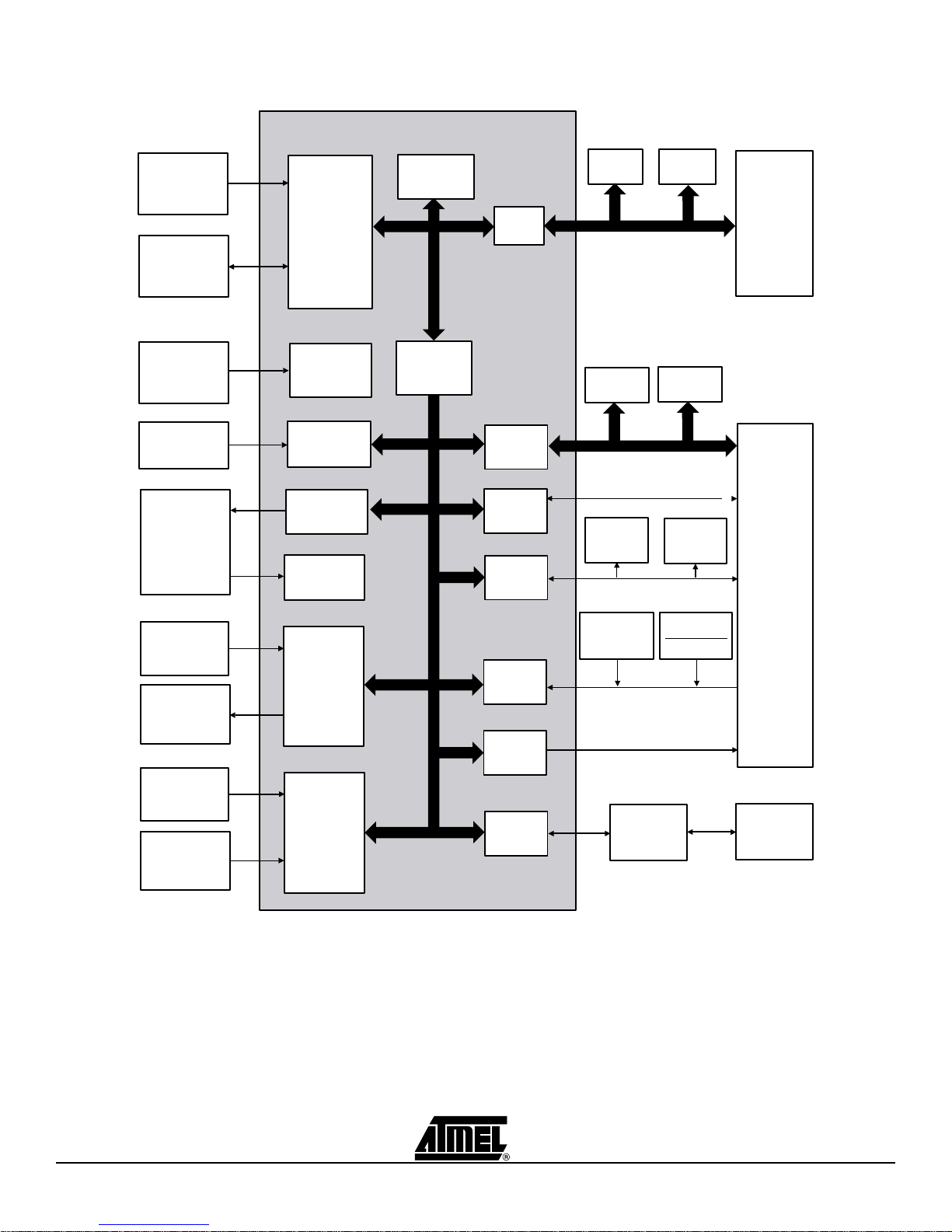
Figure 1-1.
AT91EB55 Block Diagram
AT91M55800
ASB
Clock
Generator
Reset
JTAG-ICE
Connector
APB
SRAM
Flash
LEDs
APMC
RTC
Reset
Controller
16 MHz
XTAL
ARM7TDMI
Processor
8K byte
RAM
EBI
EBI
Expansion
Connector
I
2
C
E
2
PROM
Interrupt
Controller
Push
Buttons
Reset
Controller
Watchdog
Timer
Timer
Counters
Serial
Data Flash
Serial
E
2
PROM
I/O
Expansion
Connector
Temperature
Sensor
RS232
Transceivers
DB9
Serial
Connectors
Battery
Power
Supply
32.768 kHz
XTAL
V
DDIO
and
V
DDCORE
Power
Supply
Wake Up
Push
Button
V
DDCORE
2
AMBA
Bridge
PIO
SPI
ADC
DAC
Serial
Ports
Page 8

Overview
1-4 AT91EB55 Evaluatuon Board User Guide
1709B–ATARM–07/02
Page 9
AT91EB55 Evaluatuon Board User Guide 2-1
Rev. 1709B–ATARM–07/02
Section 2
Setting Up the AT91EB55
Evaluation Board
2.1 Electrostatic
Warning
The AT91EB55 Evaluation Board is shipped in protective anti-static packaging. The
board must not be subjected to high electrostatic potentials. A grounding strap or similar
protective device should be worn when handling the board. Avoid touching the component pins or any other metallic element.
2.2 Requirements Requirements in order to set up the AT91EB55 Evaluation Board are:
n
TheAT91EB55EvaluationBoarditself
n
DC power supply capable of supplying 7V to 12V @ 1 A (not supplied)
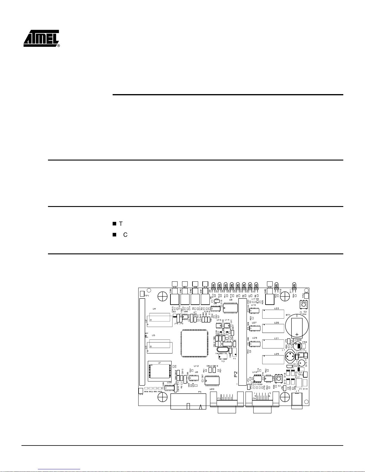
2.3 Layout Figure 2-1 shows the layout of the AT91EB55 Evaluation Board.
Figure 2-1.
Layout of the AT91EB55 Evaluation Board
128K x 8
512K x 8
128K x 8
512K x 8
AT91M55800A
33 AI
Page 10

Setting Up the AT91EB55 Evaluation Board
2-2 AT91EB55 Evaluatuon Board User Guide
1709B–ATARM–07/02
2.4 Jumper Settings JP1 is used to boot on standard or user programs. For standard operations, set it in the
STD position.
JP8 is used to select the core power supply of the AT91M55800A. Operations at 2V are
not supported on the current silicon.
For more information about jumpers and other straps, see Appendix A.
2.5 Powering Up the
Board
DC power is supplied to the board via the 2.1 mm socket (J1) shown below in Figure 2-
2. The polarity of the power supply is not critical. The minimum voltage required is 7V.
Figure 2-2.
2.1 mm Socket
The board has a voltage regulator providing +3.3V. The regulator allows the input voltage to be from 7V to 12V. When you switch the power on, the red LED marked
“POWER” will light up. If it does not, switch off and check the power supply connections.
The battery BT1 provides a 3V power supply to the Advanced Power Management Controller and the Real Time Clock (V
DDBU
). In order to power up this module, the user must
first close the JP9 jumper.
2.6 Measuring
Current
Consumption on
the
AT91M55800A
The board is designed to generate the power for the AT91 product only through the
jumpers JP5 (V
DDIO
), JP8 (V
DDCORE
)andJP9(V
DDBU
). This feature enables measurements to be made on the current consumption of the AT91 product. See Appendix A for
further details.
2.7 Testing the
AT91EB55
Evaluation Board
In order to test the AT91EB55 Evaluation board, the following procedure should be
performed:
1. Hold down the SW1 button and power up the board or generate a reset and wait
for the light sequence on each LED to complete. All the LEDs light once and the
D1 LED remains lit.
2. Release the SW1 button. The LEDs D1 to D7 light up in sequential order. If an
error is detected, all the LEDs will light up twice.
The LEDs represent the following devices:
n
D1 for the internal SRAM
n
D2 for the external SRAM
positive (+)
or
negative (-)
2.1 mm connector
Page 11

Setting Up the AT91EB55 Evaluation Board
AT91EB55 Evaluatuon Board User Guide 2-3
1709B–ATARM–07/02
n
D3 for the external Flash
n
D4 for the E2PROM with I2C access
n
D5 for the SPI data flash
n
D6 for the SPI E2PROM
n
D7 for the USART
n
D8 for the ADC and DAC
If a test is not carried out, the corresponding LED remains unlit and the test sequence
restarts.
Page 12

Setting Up the AT91EB55 Evaluation Board
2-4 AT91EB55 Evaluatuon Board User Guide
1709B–ATARM–07/02
Page 13

AT91EB55 Evaluatuon Board User Guide 3-1
Rev. 1709B–ATARM–07/02
Section 3
The On-board Software
3.1 AT91EB55
Evaluation Board
The AT91EB55 Evaluation Board contains an AT49BV16X4 Flash device programmed
with default software. Only the lowest eight 8-Kbyte sectors are used. The remaining
sectors are user-definable and can be programmed using one of the Flash downloader
solutionsofferedintheAT91library.
When delivered, the Flash device contains:
n
The Boot Software Program
n
The Functional Test Software
n
The SRAM Downloader
n
The Angel Debug Monitor
n
A Default User Boot with a Default Application
The boot, FTS and SRAM downloader are in sectors 0 and 1 of the Flash. These sectors are not locked for an easy on-board upgrade. The user must avoid overwriting this
sector.
3.2 The Boot
Software
Program
The Boot Software Program configures the AT91M55800A and thus controls the memory and other board devices.
The Boot Software Program is started at reset if JP1 is in the STD position. If JP1 is in
the USER position, the AT91M55800A boots from address 0x01010000 in the Flash,
which must have a user-defined boot.
The Boot Software Program first initializes the master clock frequency at 32 MHz, the
EBI, then executes the REMAP and checks the state of the buttons as described below.
As long as the SW1 button is pressed:
n
All the LEDs light together
n
The D1 LED remains lit until SW1 is released
n
The Functional Test Software (FTS) is started
As long as the SW2 button is pressed:
n
All the LEDs light together
n
The D2 LED remains lit until SW2 is released
Page 14

The On-board Software
3-2 AT91EB55 Evaluatuon Board User Guide
1709B–ATARM–07/02
n
The SRAM downloader is activated
n
When the SW4 button is pressed:
n
The shutdown function from AT91M55800A is activated. The power-up can be
achieved by pressing the S1 push button only (Wake-up function)
When no buttons are pressed:
n
Branch at address 0x01004000
n
The Angel Debug Monitor starts from this address by recopying itself in external
SRAM
3.3 Programmed
Default Memory
Mapping
The following table defines the mapping defined by the boot program.
The Boot Software Program, FTS and SRAM downloader are in sectors 0 and 1 of the
Flash device. Sectors 2 to 7 support the Angel Debug Monitor
Sector 24 at address 0x01100000 must be programmed with a boot sequence to be
debugged. This sector can be mapped at address 0x01000000 (or 0x0 after a reset)
when the jumper JP1 is in the USER position.
3.4 The SRAM
Downloader
The SRAM downloader allows an application to be loaded in the SRAM at the address
0x02000000 and then activates it. The boot starts it if the SW2 button is pressed at
reset.
The procedure is as follows:
1. Connect the AT91EB55 Evaluation Board to the host PC serial A connection
using the straight serial cable provided.
2. Power on or press RESET, simultaneously holding down the SW2 button. Wait
for D2 to light up and then release SW2.
3. Start the BINCOM utility, available in the AT91 Library, on the host computer:
Select the communication port (COM1 or COM2, depending on where the serial
cable is connected to the host PC) and the baud rate for communications (115200
baud, 1 stop bit, no parity), then open the file to be downloaded and send it. Wait for
the transfer to end.
4. Press any button to end the download. The control is switched to the address
0x02000000.
3.5 The Angel Debug
Monitor
The Angel Debug Monitor is located in the flash from 0x01004000 up to 0x0100FFFF.
The boot program starts it if no button is pressed.
When Angel starts, it recopies itself in SRAM in order to run faster. The SRAM used by
Angel is from 0x02020000 to 0x0203FFFF, i.e., the highest half part of the SRAM.
Table 3-1.
Memory Map
Part Name Start Address End Address Size Device
U1 0x01000000 0x011FFFFF 2-Mbyte Flash AT49BV16X4
U2 - U3 0x02000000 0x0203FFFF 256-Kbyte SRAM
Page 15

The On-board Software
AT91EB55 Evaluatuon Board User Guide 3-3
1709B–ATARM–07/02
The Angel on the AT91EB55 can be upgraded regardless of the version programmed on
it.
Note:
If the debugger is started through ICE while the Angel monitor is on, the
Advanced Interrupt Controller (AIC) and the USART channel are enabled.
Page 16

The On-board Software
3-4 AT91EB55 Evaluatuon Board User Guide
1709B–ATARM–07/02
Page 17

AT91EB55 Evaluatuon Board User Guide 4-1
Rev. 1709B–ATARM–07/02
Section 4
Circuit Description
4.1 AT91M55800A
Processor
Figure 1 in “Appendix B – Schematics” shows the AT91M55800A. The footprint is for a
176-pin TQFP package.
Strap CB15 enables the user to choose between the standard ICE debug mode and the
JTAG boundary scan mode of operation.
The operating mode is defined by the state of the JTAGSEL input detected at reset.
Jumper JP5 can be removed by the user to allow measurement of the current demand
by the whole microcontroller (V
DDIO
and V
DDCORE
). Jumper JP8 can be removed to mea-
sure the core microcontroller consumption (V
DDCORE
). See Figure 8 in “Appendix B –
Schematics.”
Jumper JP9 can be removed by the user to allow measurement of the current demand
by the APMC and RTC microcontroller modules (V
DDBU
). See Figure 8 in “Appendix B –
Schematics.”
4.2 Expansion
Connectors and
JTAG Interface
The two expansion connectors (I/O expansion connector and EBI expansion connector)
and the JTAG Interface are described below.
The I/O and EBI expansion connectors pin-outs and positions are compatible with the
other evaluation boards (except for the I/O expansion connector pin-out and position of
the EB40) so that users can connect their prototype daughter boards to any of these
evaluation boards. For the I/O expansion connector, rows A and B are position and
pinout compatible.
4.2.1 I/O Expansion
Connector
The I/O expansion connector makes the general purpose I/O (GPIO) lines, VCC3V3 and
Ground available to the user. Configuration straps CB2, CB3, CB4, CB5, CB6, CB13,
CB14 and CB17 are used to select between the I/O lines being used by the evaluation
board or by the user via the I/O expansion connector. The connector is not fitted at the
factory; however, the user can fit any 32 x 3 connector on a 0.1" (2.54 mm) pitch.
4.2.2 EBI Expansion
Connector
The schematic illustrated in Figure 4 in "Appendix B - Schematics" also shows the Bus
expansion connector, which, like the I/O expansion connector, is not fitted at the factory.
The user can fit any 32 x 2 connector on a 0.1" (2.54 mm) pitch to gain access to the
data, address, chip select, read/write, oscillator output and wait request pins. VCC3V3
and Ground are also available on this connector. Configuration strap CB1, when open,
allows the user to connect the EBI expansion connector to the MPI expansion connector
of an AT91EB63 evaluation board without fearing any conflict problem.
Page 18

Circuit Description
4-2 AT91EB55 Evaluatuon Board User Guide
1709B–ATARM–07/02
4.2.3 JTAG Interface An ARM-standard 20-pin box header (P5) is provided to enable connection of an ICE to
the JTAG inputs on the AT91. This allows code to be developed on the board without
using system resources such as memory and serial ports.
4.3 Memories The schematics in Figures 3 and 9 in "Appendix B – Schematics" show one
AT49BV16X4 2-Mbyte 16-bit Flash, one AT24C512 64-Kbyte EEPROM, one AT25256
32-Kbyte EEPROM, two 128K/512K x 8 SRAM devices and four AT45DB321 4-Mbyte
serial data Flash devices.
TheSPIdevicesareaccessiblethrougha4to16linedecoderandbyusingtheChip
Select Decode feature of the AT91 SPI peripheral (PCSDEC bit of the SPI Mode
Register).
Note: The AT91EB55 is fitted with two 128K x 8 SRAM devices and one AT45DB321 serial
DataFlash device (U21).
The AT91EB55 may be fitted with a Flash using either an AT49BV1604 (CB18 should
be closed) or an AT49BV1614 (CB18 should be open).
Strap JP1 shown on the schematic is used to select which part of 1-Mbyte of the flash is
to be accessed. This is to enable users to flash download their application in the second
part of the flash and to boot on it.
4.4 ADC and DAC
Peripheral
Connections
Two of the ADC and DAC channels are loop-backed together: DA0 on AD4 and DA1 on
AD0.
Two 2.5V voltage reference devices are fitted on the board and connected to the
DAVREF and ADVREF inputs, See Figures 6 in "Appendix B – Schematics". The user
can fit other voltage reference value devices from this family (REF19x from Analog
Devices) as the footprints are compatible.
A temperature sensor (LM61: figure 6 in "Appendix B – Schematics") is connected to the
AD1 input and is placed near the 32.768 kHz crystal quartz. It enables the user to take
into account the frequency drift due to temperature evolutions using a software program.
The V
DDCORE
witharesistorbridge(10kΩ) provides the following value:
This voltage can be measured by AD2 input and allows the user to select the running
clock accordingly.
4.5 Power and
Crystal Quartz
The board features two quartz crystals: a 32.768 kHz one connected to the RTC lowpower oscillator of the AT91M55800A and a 16 MHz one connected to the main
oscillator.
The AT91M55800A Master Clock can be derived from the 32.768 kHz crystal quartz or
the 16 MHz crystal quartz depending on the programming of the APMC registers. The
on-chip oscillators together with one PLL-based frequency multiplier and the prescaler
results in a programmable Master Clock between 500 Hz and 33 MHz.
VDDCORE
2
------------- ------------ -----
c
Page 19

Circuit Description
AT91EB55 Evaluatuon Board User Guide 4-3
1709B–ATARM–07/02
Components for the PLL filter are fitted by default on the board (Figure 6 in "Appendix B
– Schematics"). They are calculated to provide a 32 MHz (multiplier factor of 2 and settling time of 160 µs) Master Clock frequency.
The Voltage Regulator provides 3.3V to the board and will light the red POWER LED
(D11) when operating.
This Voltage Regulator can be turned off by using the APMC shutdown feature when the
JP7 jumper is closed. See Figure 8 in "Appendix B – Schematics." A wake-up push button (S1) is provided to exit this mode. Alternatively, the user can program a RTC alarm
to awake the voltage regulator.
Power can be applied via the 2.1 mm connector to the regulator in either polarity
because of the diode rectifying circuit. Another regulator allows the user to power the
AT91M55800A core with 3.3V or 2V by the mean of the JP8 jumper.
A 3V battery is provided on-board (Figure 8 in "Appendix B – Schematics") to power the
RTC and APMC (V
DDBU
). It has been provided to ensure the power supply for approxi-
mately 1 year.
4.6 Push Buttons,
LEDs, Reset and
Serial Interface
The IRQ0, TIOA0, PB17 and PB19 switches are debounced and buffered.
A supervisory circuit has been included in the design to detect and, consequently, reset
the board when the 3.3V supply voltage drops below a typical 3.0V threshold. Note that
the threshold can change, depending on the board production series. The supervisory
circuit also provides a debounced reset signal. This device can also generate the reset
signal in case of watchdog timeout as the pin NWDOVF of the AT91M55800A is connected on its input MR
.
The assertion of this reset signal will light the red RESET LED D10 and if the CLEAR
RESET push button is pressed the LED D10 will unlight.
Another supervisory circuit separately initializes the microcontroller embedded
JTAG/ICE interface when the 3.3V supply voltage drops below a typical 3.0V threshold.
Note that this voltage can change depending on the board production series. The separated reset lines allow the user to reset the board without resetting the JTAG/ICE
interface while debugging. bill
An RC device has been fitted on-board to ensure a correct power-on reset for the battery power supply modules (V
DDBU
) first power up or when V
DDBU
has been
disconnected. This RC network has been calculated to generate a valid 300 ms minimum pulse width NRSTBU signal.
The schematic Figure 5 in "Appendix B - Schematics" also shows eight general-purpose
LEDs connected to Port B PIO pins PB8 to PB15.
Two 9-way D-type connectors P3/4 are provided for serial port connection.
Serial Port A (P3) is used primarily for host PC communication and is a DB9 female connector. TXD and RXD are swapped so that a straight through cable can be used. CTS
and RTS are connected together as are DCD, DSR and DTR.
Serial Port B (P4) is a DB9 male connector with TXD and RXD obeying the standard
RS-232 pin-out. Apart from TXD, RXD and Ground, the other pins are not connected.
A MAX3223 device U10 and associated bulk storage capacitors provide RS-232 level
conversion.
Page 20

Circuit Description
4-4 AT91EB55 Evaluatuon Board User Guide
1709B–ATARM–07/02
4.7 Layout Drawing The layout diagram schematic shows an approximate floorplan for the board. This has
been designed to give the lowest board area, while still providing access to all test
points, jumpers and switches on the board. See Figure 1 in “Appendix B – Schematics.”
The board is provided with four mounting holes, one at each corner, into which feet are
attached. The board has two signal layers and two power planes.
Page 21

AT91EB55 Evaluatuon Board User Guide 5-1
Rev. 1709B–ATARM–07/02
Section 5
Appendix A – Configuration Straps
5.1 Configuration
Straps(CB1–15,
JP1–9)
By adding the I/O and EBI expansion connectors, users can connect their own peripherals to the evaluation board. These peripherals may require more I/O lines than available
while the board is in its default state. Extra I/O lines can be made available by disabling
some of the on-board peripherals or features. This is done using the configuration straps
detailed below. Some of these straps present a default wire (notified by the default mention) that must be cut before soldering the strap.
CB1 On-board NCS4 Signal
Closed
(1)
NCS4 signal is connected to the EBI expansion connector (P1 – B21)
Open NCS4 signal is not connected to the EBI expansion connector (P1 – B21).
This authorizes users to connect the EBI expansion connector of this board to
the MPI expansion connector of an AT91EB63 evaluation board without conflict
problems.
CB2 ADC0 Trigger Input Command
Closed
(1)
ADC0 trigger input (AD0TRIG) is controlled by the PA4 PIO line.
Open ADC0 trigger input (AD0TRIG) is not connected to the PA4 PIO line. This
authorizes users to connect the corresponding lines to their own resources via
the I/O expansion connector.
CB3 ADC1 Trigger Input Command
Closed
(1)
ADC1 trigger input (AD1TRIG) is controlled by the PA7 PIO line.
Open ADC1 trigger input (AD1TRIG) is not connected to the PA7 PIO line. This
authorizes users to connect the corresponding lines to their own resources via
the I/O expansion connector.
Page 22

Appendix A – Configuration Straps
5-2 AT91EB55 Evaluatuon Board User Guide
1709B–ATARM–07/02
CB4 Temperature Sensor Enabling
Closed
(1)
The temperature sensor device is connected to the ADC channel 1 (AD1)
input.
Open The temperature sensor device is not connected to the ADC channel 1 (AD1)
input. This authorizes users to connect the corresponding ADC channel to their
own resources via the I/O expansion connector.
CB5 Analog Converter Peripherals Loopback
Closed
(1)
DAC Channel 0 is connected to ADC Channel 4 for test purposes.
Open DAC Channel 0 is not connected to ADC Channel 4. This authorizes users to
connect the corresponding Analog Channels to their own resources via the I/O
expansion connector.
CB6 Analog Converters Peripherals Loopback
Closed
(1)
DAC Channel 1 is connected to ADC Channel 0 for test purposes.
Open DAC Channel 1 is not connected to ADC Channel 0. This authorizes users to
connect the corresponding Analog Channels to their own resources via the I/O
expansion connector.
CB9 On-board Boot Chip Select
Closed
(1)
NCS0 select signal is connected to the Flash memory.
Open NCS0 select signal is not connected to the Flash memory. This authorizes
users to connect the corresponding select signal to their own resources via the
EBI expansion connector.
CB10 Flash Reset
Closed
(1)
The on-board reset signal is connected to the Flash RESET input.
Open The on-board reset signal is not connected to the Flash RESET
input.
CB11 Boot Mode Strap Configuration
Open
(1)
The BMS MCU input pin is set for the microcontroller to boot on an external
16-bit memory at reset.
Closed The BMS MCU input pin is set for the microcontroller to boot on an external
8-bit memory at reset.
Page 23

Appendix A – Configuration Straps
AT91EB55 Evaluatuon Board User Guide 5-3
1709B–ATARM–07/02
CB13, CB14 I2C EEPROM Enabling
Closed
(1)
E2PROM communication is enabled.
Open E
2
PROM communication is disabled. This authorizes users to connect the
corresponding PIO to their own resources via the I/O expansion connector.
CB15 JTAGSEL
1 – 2
(1)
The MCU standard ICE debug feature is enabled.
2 – 3 IEEE 1149.1 JTAG boundary scan feature is enabled.
CB16 R(eturn) TCK ICE Signal Synchronization
1 – 2 The TCK signal from the JTAG interface can be synchronized with MCKO
signal and returns to the JTAG interface. (RTCK)
2 – 3
(1)
The TCK and RTCK ICE signals are not synchronized with MCKO.
CB17 V
DDCORE
Voltage Measurement
Closed
(1)
The V
DDCORE
power supply is connected to the ADC Channel 2 (AD2) input
through a resistor bridge (divisor ratio 1/2).
Open The V
DDCORE
power supply is not connected to the ADC Channel 2 (AD2) input.
This authorizes users to connect the corresponding ADC Channel to their own
resources via the I/O expansion connector.
CB18 Flash Configuration
Open Should be open when an AT49BV1614 is fitted on the board.
Closed Should be closed when an AT49BV1604 is fitted on the board.
JP1 User or Standard Boot Selection
2 – 3 The first half of the Flash memory is accessible at its base address.
1 – 2 The second half of the Flash memory is accessible at its base address. This
authorizes users to download their own application software in this part and to
boot on it.
Page 24

Appendix A – Configuration Straps
5-4 AT91EB55 Evaluatuon Board User Guide
1709B–ATARM–07/02
Notes: 1. Hardwired default position: To cancel this default configuration, cut (or place) the wire
(a jumper) on the board.
5.2 Power
Consumption
Measurement
Straps (JP5, JP9)
The JP5 strap enables the user to connect an ammeter to measure the AT91M55800A
global consumption (V
DDCORE
and V
DDIO
) when V
DDCORE
power supply is derived from
V
DDIO
(JP8 in 3V3 position). The user can measure the core consumption by connecting
another ammeter between JP8 1 – 2or2– 3 depending on the power supply used to
power the core.
The JP9 strap enables the user to connect an ammeter to measure the AT91M55800A
APMC and RTC modules battery backup consumption (V
DDBU
).
5.3 Ground Links
(JP6)
The JP6 strap allows the user to connect the electrical and mechanical ground.
JP2 Push Button Enabling
Open SW1-4 inputs to the AT91 are valid.
Closed SW1-4 inputs to the AT91 are not valid. This authorizes users to connect the
corresponding PIO to their own resources via the I/O expansion connector.
JP3 RS-232 Driver Enabled
Open The RS-232 transceivers are enabled.
Closed The RS-232 transceivers are disabled. This authorizes users to connect the
corresponding PIO to their own resources via the I/O expansion connector.
JP7 Power Shut-down Feature
Open The power supply shut-down feature is disabled.
Closed The power supply shut-down feature is enabled. The user may shut-down the
board main power supply by using the APMC shut-down feature. The system
may be awakened by pushing the S1 Wake-Up push button or by programming
an alarm in the RTC module.
JP8 Core Power Supply Selection
2 – 3 The MCU core is powered by a 3.3V power supply.
1 – 2 Not supported on the current microcontroller revision.
Page 25

Appendix A – Configuration Straps
AT91EB55 Evaluatuon Board User Guide 5-5
1709B–ATARM–07/02
5.4 Increasing
Memory Size
The AT91EB55 evaluation board is supplied with two 128K bytes x 8 SRAM memories.
If, however, the user needs more than 256K bytes of memory, the devices can be
replaced with two 512K x 8, 3.3V, 10/15 ns SRAMs, giving in total 1024K bytes.
The AT91EB55 evaluation board is supplied with one 4-MB Serial Data Flash. If the
user needs more storage memory, 3 additional footprints are provided to fit AT45DB321
devices giving a total of 16M bytes.
Page 26

Appendix A – Configuration Straps
5-6 AT91EB55 Evaluatuon Board User Guide
1709B–ATARM–07/02
Page 27

AT91EB55 Evaluatuon Board User Guide 6-1
Rev. 1709B–ATARM–07/02
Section 6
Appendix B – Schematics
6.1 Schematics The following schematics are appended:
n
Figure 6-1 PCB Layout
n
Figure 6-2 AT91EB55 Blocks Synopsis
n
Figure 6-3 EBI Memories
n
Figure 6-4 I/O and EBI Expansion Connectors
n
Figure 6-5 Push Buttons, LEDs and Serial Interface
n
Figure 6-6 AT91M55800A
n
Figure 6-7 Reset and JTAG Interface
n
Figure 6-8 Power Supply
n
Figure 6-9 SPI and I2CMemories
The pin connectors are indicated on the schematics:
n
P1 = EBI Expansion – External Bus Interface (Figure 6-4)
n
P2 = I/O Expansion Connector (Figure 6-4)
n
P3 = Serial A - Serial Interface (Figure 6-5)
n
P4 = Serial B– Serial Interface (Figure 6-5)
n
P5 = JTAG Interface (Figure 6-7)
Page 28

Appendix B – Schematics
6-2 AT91EB55 Evaluatuon Board User Guide
1709B–ATARM–07/02
Figure 6-1.
PCB Layout
128K x 8
512K x 8
128K x 8
512K x 8
AT91M55800A
33 AI
Page 29

Appendix B – Schematics
AT91EB55 Evaluatuon Board User Guide 6-3
1709B–ATARM–07/02
Figure 6-2.
AT91EB55 Blocks Synopsis
MICRCONTROLLOR
micro / Rst / Wchdog / JTAG co.
SCL
SDA
MISO
SPCK
MOSI
EBI_[0..49]
IOB_[0..67]
NPCS[0..3]
SHDN
EBI MEMORIES
memories connected on EBI
EBI_[0..49]
IOB_54
SERIAL MEMORIES
SERIAL MEMORIES
NPCS[0..3]
IOB_[68..71]
SCL
MOSI
MISO
SPCK
SDA
EBI_41
INPUT / OUTPUT ON BOARD
Serial Connectors / P.B. / LED
IOB_[0..53]
Extension Connectors
Extension Connectors
IOB_[0..71]
EBI_[0..49]
SUPPLY and RTC SAVE
power supply / battery
SHDN
IOB_[0..67]
MISO
EBI_[0..49]
IOB_[68..71]
NPCS[0..3]
EBI_[0..49]
EBI_[0..49]
IOB_[0..71]
MISO
SCL
IOB_54
IOB_[0..53]
SCL
NPCS[0..3]
IOB_[0..71]
IOB_[0..71]
SPCK
SDA
EBI_41
IOB_[0..71]
SHDN
SHDN
EBI_[0..49]
SDA
SPCK
MOSI
IOB_[0..71]
MOSI
MICROCONT ROLLER
Page 30

Appendix B – Schematics
6-4 AT91EB55 Evaluatuon Board User Guide
1709B–ATARM–07/02
Figure 6-3.
EBI Memories
VCC3V3
VCC3V3
VCC3V3VCC3V3VCC3V3VCC3V3
VCC3V3
VCC3V3 VCC3V3
VCC3V3
VCC3V3 VCC3V3
VCC3V3
VCC3V3
VCC3V3
NWR0/NWE
NRST
NCS0
NRD/NOE
A20B
NCS1
NWR1/NUB
D11
D8
A6
A18
A1
D10
A5
A2
A3A7A4
A19
A8
D9
NRD/NOE
D14
A14
D15
A16
D13
A15
D12
A13
A12
A17
A9
A11
A10
A4
A19
D1
D2
NWR0/NWE
A8
A5
A18
A7
D0
A2
A6
D3
A3
A1
NCS1
A14
A15
D6
A11
A13
D5
A16
A10
A12
NRD/NOE
A17
D4
A9
D7
A11
A13
D1
A18
A4
A5
A8
D8
NRD/NOE
D7
A1
NWR0/NWE
D3
A1
A19
A13
NCS1
D14
A17
A19
D0
A12
A16
A4
D11
D5
D9
A12
D2
A10
D10
A6
A9
NWR1/NUB
A7
A16
D15
A5
A3
NCS1
A8
A14 A14
A17
A3
A9
A15
A6 A11
D13
A2
A18
A10
D6
A2
A15
NRD/NOE
D12D4
A7
IOB_54 AE20
D[0..15]
EBI_[0..15]
D9
D0
A[0..19]
EBI_[16..35]
D2
D12
D3
A12
A18
D10
A15
CTL5 NRST
NCS0
D1
D11
D7
D6
A14
CTL0 NWR0/NWE
A13
D8
A1
A16
A17 D15
A2
NCS[0..7]
EBI_[42..49]
D13
CTL2 NRD/NOE
A4
CTL1 NWR1/NUB
A19
NCS1
A[0..19]
A9A7A6
A8
D[0..15]
D5
A5
A10
A11
D14
D4
A3
CTL[0..5]
EBI_[36..41]
A20B
C5
100nF
R1
100k
12
R2
100k
12
U3
IDT71V424S10Y
12345
1415161718
2021222324
32
33
6
13
31
8
11
12 25
26
29302710
34
35
9 28
7
19
36
A0A1A2A3A4
A5A6A7A8A9
A10
A11
A12
A13
A14
A15
A16
CS
WE
OE
D1D2D3 D4
D5
D6
D7
VCCGND
A17
A18
VCC GND
D0
NC
NC
U2
IDT71V424S10Y
12345
1415161718
2021222324
32
33
6
13
31
8
11
12 25
26
29302710
34
35
9 28
7
19
36
A0A1A2A3A4
A5A6A7A8A9
A10
A11
A12
A13
A14
A15
A16
CS
WE
OE
D1D2D3 D4
D5
D6
D7
VCCGND
A17
A18
VCC GND
D0
NC
NC
U5
IDT71424S10PH
34567
1617181920
2627282930
38
39
8
15
37
101314 31
32
35363312
40
41
1
2
11 34
43
44
9
21
22 23
24
25
42
A0A1A2A3A4
A5A6A7A8A9
A10
A11
A12
A13
A14
A15
A16
CS
WE
OE
D1D2D3 D4
D5
D6
D7
VCCGND
A17
A18
NC
NC
VCC GND
NC
NC
D0
NC
NC NC
NC
NC
NC
U4
IDT71424S10PH
34567
1617181920
2627282930
38
39
8
15
37
101314 31
32
35363312
40
41
1
2
11 34
43
44
9
21
22 23
24
25
42
A0A1A2A3A4
A5A6A7A8A9
A10
A11
A12
A13
A14
A15
A16
CS
WE
OE
D1D2D3 D4
D5
D6
D7
VCCGND
A17
A18
NC
NC
VCC GND
NC
NC
D0
NC
NC NC
NC
NC
NC
C1
100nF
C2
100nF
C3
100nF
C4
100nF
CB9
1 2
CB10
1 2
JP1
jumper_3P
1
2
3
1
U6A
74LVC04AD
1 2
U1
AT49BV1604-90TC
25242322212019
18
8764321
481716
15910141326112812 27
46
37
47
293133353840424430323436394143545
A0A1A2A3A4A5A6A7A8A9A10
A12
A13
A14
A15
A16
A17
A18
A19 / (RDY / BUSY)
NC / (A19)NCNC
NC / VppCEWEOERESET GND
GND
VCC
(BYTE) / VCCQ
I/O0
I/O1
I/O2
I/O3
I/O4
I/O5
I/O6
I/O7
I/O8
I/O9
I/O10
I/O11
I/O12
I/O13
I/O14
A11
(A-1) / I/O15
CB18
1 2
EBI_[0..49]
IOB_54
STD BOOT
512k 512k
128k 128k
128k
512k512k
128k
USER BOOT
layout for TSSOP 400mil.
layout for SOJ 400mil.
Page 31

Appendix B – Schematics
AT91EB55 Evaluatuon Board User Guide 6-5
1709B–ATARM–07/02
Figure 6-4.
I/O and EBI Expansion Connectors
VCC3V3
VCC3V3
VCC3V3
VCC3V3
VCC3V3
VCC3V3
VCC3V3
VCC3V3
VCC3V3
VCC3V3
VCC3V3
VCC3V3
PA9
PA10
PA11
PA12
PA13 PA0
PA1
PA2
PA3
PA4
PA5
PA6
PA7
PA8
PA14
PA15
PA16
PA17
PA18
PA19
PA20
PA21
PA22
PA24
PA25
PA23
PA[0..25]
PB0
PB1
PB2
PB8
PB9
PB10
PB11
PB12
PB18
PB3
PB4
PB5
PB19
PB20
PB21
PB22
PB23
PB24
PB25
PB26
PB27
PB13
PB14
PB15
PB16
PB17
PB6
PB7
PB[0..27]
AD0
AD1
AD2
AD3
AD4
AD6
AD5
AD7
DA0
DA1
DA[0..1]
AE20
AE21
AE22
AE23
AE[20..23
NSPICS8
NSPICS7
NSPICS5
NSPICS6
D10
A7
A0
D6
D12
A10
A6
D15
A13A3A11D3A9
A12D8A18D4A16
A14
A8
D2
A2
D9
D14
D7
A17
D5
D0 D1
A15
CTL1
D11
CTL5
D13
A5
A1
A4
CTL3
NSPICS[5..8]
IOB_[68..71]
A19
A[0..19] EBI_[16..35]
CTL0
CTL2
CTL4
CTL[0..5]
CTL[0..5] EBI_[36..41]
NCS2
NCS6
NCS5
NCS3
NCS[0..7]
NCS[0..7] EBI_[42..49]
NCS7
NCS0 NCS1
NSC4_1
D[0..15] EBI_[0..15]
AD[0..7
IOB_[60..67]
AD[0..7]
IOB_[58..59]
DA[0..1]
IOB_[54..57]
AE[20..23]
IOB_[26..53]
PB[0..27]
PA[0..25]
IOB_[0..25]
NCS4
P2B
I/O Ext. Conn.
B1B2B3B4B5B6B7B8B9
B10
B11
B12
B13
B14
B15
B16
B17
B18
B19
B20
B21
B22
B23
B24
B25
B26
B27
B28
B29
B30
B31
B32
PB19 / TCLK0
PB20 / TIOA0
PB21 / TIOB0
PB22 / TCLK1
PB23 / TIOA1
PB24 / TIOB1
PB25 / TCLK2
PB26 / TIOA2
PB27 / TIOB2
PA0 / TCLK3
PA1 / TIOA3
PA2 / TIOB3
PA3 / TCLK4
PA4 / TIOA4
PA5 / TIOB4
PA6 / TCLK5
PA7 / TIOA5
PA8 / TIOB5
PA14 / SCK0
PA15 / TXD0
PA16 / RXD0
PA17 / SCK1
PA18 / TXD1 / NTRI
PA19 / RXD1
PA20 / SCK2
PA21 / TXD2
PA22 / RXD2
PA24 / MISO
PA25 / MOSI
PA23 / SPCK
NSPICS5
NSPICS6
P2A
I/O Ext. Conn.
A1A2A3A4A5A6A7A8A9
A10
A11
A12
A13
A14
A15
A16
A17
A18
A19
A20
A21
A22
A23
A24
A25
A26
A27
A28
A29
A30
A31
A32
GND
VCC3V3
PA9 / IRQ0
PA10 / IRQ1
GND
PA11 / IRQ2
VCC3V3
PA12 / IRQ3
GND
PA13 / FIQ
VCC3V3
PB3 / IRQ4
PB4 / IRQ5
GND
PB5 / IRQ6
PB0
GND
PB1
PB2
PB8
PB9
VCC3V3
PB10
PB11
PB12
PB18 / BMS
GND
NSPICS8
NSPICS7
GND
VCC3V3
GND
P2C
I/O Ext. Conn.
C1C2C3C4C5C6C7C8C9
C10
C11
C12
C13
C14
C15
C16
C17
C18
C19
C20
C21
C22
C23
C24
C25
C26
C27
C28
C29
C30
C31
C32
GND
VCC3V3
PB13
PB14
PB15
PB16
PB17
VCC3V3
GND
A20
A21
A22
A23
GND
DA0
GND
DA1
GND
PB6 / AD0TRIG
GND
AD0
AD1
AD2
AD3
GND
AD4
AD5
AD6
AD7
GND
PB7 / AD1TRIG
GND
P1B
EBI Ext. Con.
B1B2B3B4B5B6B7B8B9
B10
B11
B12
B13
B14
B15
B16
B17
B18
B19
B20
B21
B22
B23
B24
B25
B26
B27
B28
B29
B30
B31
B32
GND
NWR1 / NUB
NWAIT
-
NCS1
NCS3
NRST
A1A3A5
A7
GND
A9
A11
A13
A15
VCC3V3
A17
A19
NCS6
NCS4
GND
D1D3D5
D7
VCC3V3
D9
D11
D13
D15
GND
P1A
EBI Ext. Con.
A1A2A3A4A5A6A7A8A9
A10
A11
A12
A13
A14
A15
A16
A17
A18
A19
A20
A21
A22
A23
A24
A25
A26
A27
A28
A29
A30
A31
A32
GND
NWR0 / NWE
NRD / NOE
MCK0
NCS0
NCS2
VCC3V3
A0 / NLBA2A4A6GNDA8A10
A12
A14
VCC3V3
A16
A18
NCS7
NCS5
GNDD0D2D4D6
VCC3V3D8D10
D12
D14
GND
CB1
1 2
EBI_[0..49] IOB_[0..71]
EBI Extension Connector I/O Extension Connector
Page 32

Appendix B – Schematics
6-6 AT91EB55 Evaluatuon Board User Guide
1709B–ATARM–07/02
Figure 6-5.
Push Buttons, LEDs and Serial Interface
VCC3V3 VCC3V3
VCC3V3
VCC3V3
VCC3V3
VCC3V3
VCC3V3
VCC3V3
VCC3V3
VCC3V3
VCC3V3
VCC3V3
VCC3V3
VCC3V3
VCC3V3
VCC3V3
VCC3V3
VCC3V3
VCC3V3
VCC3V3
VCC3V3
VALBP
IRQ0PA9
PB17
PB19
PB8
PB9
PB10
PB11
PB12
PB13
PB14
PB15
VALBP
DSR0
RTS0
CTS0
DTR0
DCD0
TX0
RX0
TX1
TXD0PA15
PA18 TXD1
PA16 RXD0
PA19 RXD1
PA[0..25]
RX1
PA[0..25]
IOB_[0..25]
PB[0..27]
IOB_[26..53]
PA9
TIOA0PB20
EN
U9
74LV125D
14
7
124
5109
13
12
3
6
8
11
R3
100K
C10
47nF
SW1
TP 33
R4
100K
C11
47nF
SW2
TP 33
R14
100K
SW3
TP 33
SW4
TP 33
C14
47nF
R15
100K
C15
47nF
R5
100k
D1
Red LED
R6
100R
D2 R7
100R
D3 R8
100R
D4 R9
100R
D5 R10
100R
R11
100R
D6
R12
100R
D7
D8 R13
100R
EN
EN
U8
74LV244D
GND SIGNAL
VCC3V3
12468
1911131517 3
10
579
12
14
16
18
20
C17
100nF
C19
100nF
C18
100nF
C22
100nF
C21
22pF
P3
Sub D 9b F
594837261
C20
22pF
C23
22pF
C26
22pF
C27
22pF
U10
MAX3223ECAP
1
14 20
11
18
16
9
151013
12
17
8
245
6
3
7
19
EN
FORCEON FORCEOFF
INVALID
GND
R1IN
R2IN
R1OUT
R2OUT
T1IN
T2IN
T1OUT
T2OUT
C1+
C1-
C2+
C2-
V+
V-
VCC
R16
100k
P4
Sub D 9b M
594837261
C25
10nF
R17
100K
C13
100nF
C12
100nF
1 2
C16
100nF
R43
100k
R42
100k
R44
100k
R45
100k
JP2
jumper_NO
1 2
JP3
jumper_NO
1 2
C24
22pF
IOB_[0..53]
Usart 0:
SERIAL A
Usart 1:
SERIAL B
Page 33

Appendix B – Schematics
AT91EB55 Evaluatuon Board User Guide 6-7
1709B–ATARM–07/02
Figure 6-6.
AT91M55800A
GNDBU
GNDBU
GNDBU
GNDBU
VDDBU
VDDPLL
VDDBU
VDDA
VDDIO
VDDPLL
VDDCORE
VDDCORE
VDDCORE
VDDCORE
VDDIO
VCC3V3
VCC3V3
VCC3V3
VDDIO
VDDIO
VDDIO
GNDPLL
GNDA
VDDCORE
VCC3V3
VCC3V3
JTAG[0..4]
WAKEUP
NRST
NWDOVF
JTAGSEL
MCKO
AD1
GNDA
GNDA
JTAG0
NPCS2
PLLRC
DAVREF
VDDCORE
NWDOVF
VDDIO
JTAG[0..4]
AD3
NPCS3
JTAG2
NRSTBU
AD5
JTAGSEL
JTAG1
XOUT32
DAVREF
AD6
AD4
JTAG3
ADVREF
AD7
VDDIO
VDDIO
XIN32
VDDCORE
AD0 ADVREF
VDDIO
XOUT
NPCS0
VDDIO
VDDIO
XIN
NPCS1
VDDCORE
VDDCORE
AD1
JTAG4
AD2
vt
NWAITCTL3
VDDIO
VDDIO
VDDIO
VDDIO
vt
VDDA
GNDA
GNDA
GNDA
VDDA
VDDA
GNDA
GNDA
VDDA
GNDA
PA24
PA12
PA8
PA5
AE22
PA10
PA0
AE23
PA7 TIOA5
AD3
AD6
AD4
PA17
PA14
PA15
PA2
PA[0..25]
CTL5
JTAGSEL
PA[0..25]
AD2
PA4 TIOA4
PA[0..25]
IOB_[0..25]
IOB_[54..57]
AE[20..23]
PA7
PA1
IOB_[58..59]
DA[0..1]
DA1
PA20
PA18
PB7 AD1TRIG
AE[20..23]
DA1
AE20
DA0
PA25
AD1
PA16
PA13
PA4
AD5
AD0
PA22
PA11
PA6
PB6 AD0TRIG
IOB_[60..67]
AD[0..7]
DA0
PA21
AE21
AD7
PA3
PA9
PA23
NWDOVF
PA19
PB25
PB19
PB7
PB15
PB[0..27]
PB12
BMS PB18
PB[0..27]
PB9
PB11
PB6
PB21
PB10
PB1
PB23
PB5
PB13
PB0
PB22
PB20
PB26
PB4
PB14
PB3
PB17
PB24
PB18
IOB_[26..53]
PB[0..27]
PB8
PB2
PB27
PB16
CTL4
D14
CTL5
A9
A7
D[0..15]
EBI_[0..15]
CTL4
A12
A1
D10
CTL[0..5]
A3
CTL[0..5]
EBI_[36..41]
D6
A16
D4
NCS4
D9
NCS[0..7]
NCS[0..7]
A6
A17
A8A0A11
NCS5
D7
CTL0
A10
A18
D15
NCS1
NCS0
A[0..19]
A19
NCS[0..7]
EBI_[42..49]
NCS3
NCS7
A4
CTL1
CTL2
A2
D0
D1
D11
D8
D13
NCS2
A5
NCS6
A13
D2
D[0..15]
A[0..19]
EBI_[16..35]
A15
D12
D3
CTL3
A14
D5
C29
100nF
C49
100nF
C50
100nF
C28
100nF
C42
100nF
U13
LM61BIM3
132
VCC
GND
Vout
Y2
Qtz 32,768kHz
1 2
Y1
osc 32,768KHz
1
3
2
4
NC/ENABLE
OUT
GND
VCC
Y4
Qtz 16MHz
1 2
Y3
Osc 16MHZ
1
3
2
4
NC/ENABLE
OUT
GND
VCC
R21
100k
R19
100k
R20
287R 1%
1 2
U14
REF192GS
123
4 5
678
TPVsSLEEP
GND TP
OUTPUT
NC
NC
U15
REF192GS
123
4 5
678
TPVsSLEEP
GND TP
OUTPUT
NC
NC
R41
100K
C30
100nF
C48
1 2
C51
100nF
+
C3
1µF / 16
C39
100nF
+
C41
10µF / 16V
C43
1 2
+
C4
1µF / 16
C47
1 2
C36
100nF
C44
1 2
R18
270K
R46
100k
R48
100k
C92
100nF
C93
100nF
C91
100nF
CB11
1 2
CB12
1 2
CB4
1 2
CB7
1 2
CB8
1 2
CB5
1 2
CB6
1 2
C38
100nF
C31
100nF
C32
100nF
+
C33
1µF / 16V
CB3
1 2
CB2
1 2
C46
680pF 10%
12
C45
68pF 10%
12
CB17
1 2
R56
100K
R57
100K
7
9
1011121314
1718192021222324252627
28
3132333435363738394041
42
45
46
47
48
49
50
51
52
53
54
55
56
57
58
59
60
61
62
63
64
65
66
67
73
74
75
117
116
115
114
113
112
111
110
109
108
107
106
104
103
102
99
91
175
174
173
172
171
170
169
168
167
166
165
164
148
147
345
6
1
2
15
16
29
30
43
44
8
68
70
71
72
69
76
77
78
79
80
81
82
83
84
85
86
87
88
89
90
98979695949392
100
101
118
119
120
121
122
123
124
125
126
127
128
129
130
131
132
133
134
135
136
137
138
105
139
140
141
142
143
144
145
146
149
150
151
152
153
154
155
156
157
158
159
160
161
162
163
176
A0/NLBA2A3A4A5A6A7
A8A9A10
A11
A12
A13
A14
A15
A16
A17
A18
A19
A20
A21
A22
A23D0D1D2D3D4D5D6D7
GND
GND
D8
D9
D10
D11
D12
D13
D14
D15
PB19 / TCLK0
PB20 / TIOA0
PB21 / TIOB0
PB22 / TCLK1
VDDIO
GND
PB23 / TIOA1
PB24 / TIOB1
PB25 / TCLK2
PB26 / TIOA2
PB27 / TIOB2
PA0 / TCLK3
PA1 / TIOA3
VDDIO
GND
PA7 / TIOA5
VDDA
GNDBU
SHDN
WAKEUP
GND
NRSTBU
XOUT32
XIN32
VDDBU
PLLRC
GNDPLL
XOUT
VDDPLL
GND
VDDIO
PA27 / NPCS1
PA19 / RXD1
VDDCORE
NUB / NWR1
NWE / NWRO
NOE / NRD
NWAIT
NRST
NTRST
TCK
TDO
TDI
TMS
JTAGSEL
GND
VDDIO
NCS0
NCS1
NCS2
NCS3
GND
GND
VDDIO
GND
VDDIO
GND
VDDCORE
VDDIO
A1
PA2 / TIOB3
PA4 / TIOA4
PA5 / TIOB4
PA6 / TCLK5
PA3 / TCLK4
PA8 / TIOB5
PA9 / IRQ0
PA10 / IRQ1
PA11 / IRQ2
PA12 / IRQ3
PA13 / FIQ
PA14 / SCK0
PA15 / TXD0
PA16 / RXD0
PA17 / SCK1
PA18 / TXD1 / NTRI
VDDCORE
VDDIO
GND
GND
PA26 / NPCS0 / NSS
PA25 / MOSI
PA24 / MISO
PA23 / SPCK
PA22 / RXD2
PA21 / TXD2
PA20 / SCK2
PA28 / NPCS2
PA29 / NPCS3
AD0
AD1
AD2
AD3
AD4
AD5
AD6
AD7
ADVREF
DAVREF
DA0
DA1
GNDA
VDDCORE
VDDIO
GND
GND
NCS4
NCS5
NCS6
NCS7
XIN
PB0
PB1
PB2
PB3 / IRQ4
PB4 / IRQ5
PB5 / IRQ6
PB6 / AD0TRIG
PB7 / AD1TRIG
PB8
PB9
PB10
PB11
PB12
PB13
PB14
PB15
PB16
PB17
NWDOVF
MCKO
VDDIO
GND
PB18 / BMS
VDDIO
RR4
100k
1 8
2 7
3 6
4 5
RR3
100k
1 8
2 7
3 6
4 5
RR1
100k
1 8
2 7
3 6
4 5
RR2
100k
1 8
2 7
3 6
4 5
NPCS[0..3]
IOB_[0..67]
EBI_[0..49]
SDA
SCL
MOSI
SPCK
MISO
SHDN
REF 2.5V
REF 2.5V
Default
boot Mode :
16 Bits
U12
AT91M55800A - 33AI
Page 34

Appendix B – Schematics
6-8 AT91EB55 Evaluatuon Board User Guide
1709B–ATARM–07/02
Figure 6-7.
Reset and JTAG Interface
VCC3V3
VCC3V3
VCC3V3
VCC3V3
VCC3V3VCC3V3
VDDBU
GNDBU
VCC3V3
VCC3V3
VCC3V3
VCC3V3
VCC3V3
NWDOVF
NRST
WAKEUP
JTAG[0..4]
JTAGSEL
MCKO
RSTLEDRSTLEDRSTLED
PBRST
CTL6
NRST
G1
G2
G3
G4
G5
JTAG0 JTAG1 JTAG2 JTAG3
JTAG4 NRST
NRST
CTL5
PBRST
JTAGSEL
G9
G2G5G1
G8
G6
G9
G3
G7
G7
G4
G6
G8
CLRSTLED
CLKRSTLED
JTAG1
JTAG0
JTAG2
JTAG4
TCK
JTAG3
TCK
RTCK
TCK
JTAG3
D11
Red LED
SW5
TP 33
D10
Red LED
R24
100R
R23
100R
U17
MAX6315US27D1-T
1 4
32
GND VCC
MR
RST
R25
100k
R22
100k
D9
BAS216
C53
100nF
U18
MAX6315US27D1-T
1 4
32
GND VCC
MR
RST
R27
100k
R26
100k
S1
B.P.
C72
10nF
C74
10nF
C76
10nF
C82
10nF
C73
10nF
C78
10pF
C79
10pF
C80
10pF
C81
10pF
C84
10pF
C85
10pF
C94
100nF
C71
10nF
1
U6F
74LVC04AD
13 12
CB15
1
2
3
C52
100nF
C95
100nF
1
U6E
74LVC04AD
11 10
1
U6D
74LVC04AD
9 8
1
U6C
74LVC04AD
5 6
7
14
C75
10nF
C77
10nF
C83
10nF
C86
10nF
S2
B.P.
R54
100k
SC11D
R
U16
74LVC74AD
14
7
432
1
101112
13
569
8
1
U6B
74LVC04AD
3 4
JTAG
P5
HE10 2x10
13579
1113151719
24681012141618
20
VCC
NTRST
TDI
TMS
TCK
TCK
TDO
NRSTNCNC
VCC
GND
GND
GND
GND
GND
GND
GND
GND
GND
SC11D
R
U30
74LVC74AD
14
7
432
1
101112
13
569
8
C96
100nF
CB16
1
2
3
3V3 SUPPLYRESET
RESET
WAKEUP
ICE
IEEE
CLEAR
RESET LED
Page 35

Appendix B – Schematics
AT91EB55 Evaluatuon Board User Guide 6-9
1709B–ATARM–07/02
Figure 6-8.
Power Supply
VCC3V3
VDDCORE
VDDBU
GNDBU
VDDIO
VDDPLL
VDDA
GNDPLLGNDBU GNDA
VCC3V3 VCC1V8
VDDIO
VSAVE=3V
SHDN_2
SHDN_1
C54
100nF
F1
1000m A/30V
D14
SMT6T15CA
C57
10µF / 25V
U19
LT1507CS8-3.3
2 3754
1
8
6
VIN VSW
SENSESYNC
SHTDN
BOOST
VC
GND
D12
1N914
L1
10µH
D15
1N5817
+
C58
100µF / 10V
C60
3,3nF / 10%
C55
22pF / 25V
BT1
3V Button Pile
C64
1µF 10%
R29
OR
R30
not use
C61
1µF 10%
C62
1µF 10%
+
C63
10µF / 16V
D18
10MQ100N
D19
10MQ100N
D16
10MQ100N
D17
10MQ100N
TP2
Test Point Corner 2
TP3
Test Point Corner 3
TP1
Test Point Corner 1
TP4
Test Point Corner 4
R50
Radj
U20
LT1503CS8-2
4 132
6
8
5 7
Vin Vout
C1+
C1-
C2+
C2-
SHDN/SS
GND
J1
Jack Dia.2.1mm
C59
22pF / 25V
JP6
jumper_NO
1 2
JP7
jumper_NO
1 2
JP5
jumper_NO
1 2
JP9
jumper_NO
1 2
JP8
jumper_3P
1
2
3
+
C58B
100µF / 10V
C57B
10µF / 25V
SH1
shield
1
1
R55
100K 5%
SHDN
RTC SAVE
SHDN
VDDCORE=2.0V
VDDCORE=3.3V
I Vddcore
I Vddbu
I Vddio
Vddbu=1V84 with R30=620k R29=330k
Vddbu=3V with R29=0R and R30 off
Page 36

Appendix B – Schematics
6-10 AT91EB55 Evaluatuon Board User Guide
1709B–ATARM–07/02
Figure 6-9.
SPI and I2CMemories
VCC3V3
VCC3V3VCC3V3VCC3V3
VCC3V3
VCC3V3
VCC3V3
VCC3V3
VCC3V3
VCC3V3 VCC3V3
VCC3V3VCC3V3
VCC3V3
VCC3V3
VCC3V3
VCC3V3
SCL1
NPCS0
NPCS1
NPCS2
VCC3V3
NSPICS8
NSPICS0
MOSI
MISO
SPCK
NSPICS[5..8]
NSPICS4
NSPICS3
NRST
NSPICS1
NRST
NSPICS2
NRST
NPCS3
NSPICS0
NSPICS1
NSPICS2
NSPICS3
NSPICS4
NSPICS5
NSPICS6
NSPICS7
MOSI
MISO
SPCK
MOSI
MISO
SPCK
MOSI
MISO
SPCK
MOSI
MISO
SPCK
NRSTEBI_41
SDA1
R31
100k
BIN/OCT
0
7654321
EN
&
421
U27
74LV138D
168
12364
5
1514131211109
7
BIN/OCT
0
7654321
EN
&
421
U29
74LV138D
168
12364
5
1514131211109
7
C65
100nF
R40
100k
U23
AT24C512W1-10SC-2.7
12
11
2
1
10
20
3456789
13141516171819
SCL
SDA
A1
A0
GND
VCC
NCNCNCNCNCNCNC
NCNCNCNCNC
NC
WP
R32
100k
R34
100k
C70
100nF
C69
100nF
R37
100k
R39
100k
C66
100nF
R33
100k
R35
100k
C68
100nF
R36
100k
R38
100k
U21
AT45DB321-TC
132
141516
13
456
9
101112
171819202122232425262728293031
3287
RDY/BUSY
WP
RESET
SCKSISOCSNCNCNCNCNCNCNC
NCNCNCNCNCNCNCNCNCNCNCNCNCNCNC
NC
GND
VCC
U26
AT45DB321-TC
132
141516
13
456
9
101112
171819202122232425262728293031
3287
RDY/BUSY
WP
RESET
SCKSISOCSNCNCNCNCNCNCNC
NCNCNCNCNCNCNCNCNCNCNCNCNCNCNC
NC
GND
VCC
U22
AT45DB321-TC
132
141516
13
456
9
101112
171819202122232425262728293031
3287
RDY/BUSY
WP
RESET
SCKSISOCSNCNCNCNCNCNCNC
NCNCNCNCNCNCNCNCNCNCNCNCNCNCNC
NC
GND
VCC
U25
AT45DB321-TC
132
141516
13
456
9
101112
171819202122232425262728293031
3287
RDY/BUSY
WP
RESET
SCKSISOCSNCNCNCNCNCNCNC
NCNCNCNCNCNCNCNCNCNCNCNCNCNCNC
NC
GND
VCC
U28
AT25256W-10SC-2.7
1325
6
748
CS
WPSO
SI
SCK
HOLD
GND
VCC
C67
100nF
C89
100nF
C90
100nF
R51
100k
R52
100K
R53
100K
CB13
1 2
CB14
1 2
IOB_[68..71]
NPCS[0..3]
SDA
SCL
MOSI
SPCK
MISO
EBI_41
Page 37

AT91EB55 Evaluatuon Board User Guide 7-1
Rev. 1709B–ATARM–07/02
Section 7
Appendix C – Bill of Material
Table 7-1.
Bill of Material
Item Qty Reference Part Designation
11BT1 3VButtonPile
Li/MnO2 3V 180 mAH pile UL:
MH13654(N)
22CB16
3 position jumper (jumper
between 2-3)
3
(1)
3 CB18 CB_NO
If AT49BV1614-90TC is used,
do not connect the jumper
441
C1, C2, C3, C4, C5,
C12, C13, C16, C17,
C18, C19, C22, C28,
C29, C30, C31, C32,
C36, C38, C39, C42,
C49, C50, C51, C52,
C53, C54, C65, C66,
C67, C68, C69, C70,
C89, C90, C91, C94,
C95, C96
100 nF Ceramic X7R/10V
5 4 C10, C11, C14, C15 47 nF Ceramic X7R/10V
66
C20, C21, C23, C24,
C26, C27
22 pF Ceramic NPO/10V
711
C25, C71, C72, C73,
C74, C75, C76, C77,
C82, C83, C86
10 nF Ceramic X7R/16V
8 3 C33, C37, C40 1 µF/16V Tantalum 16V/10%/TAJ
9 2 C41, C63 10 µF/16V Tantalum 16V/10%/TAJ
10 3 C43, C47, C48 10 pF Ceramic NPO/10V/5%
11 1 C44 4 - 25 pF
Adjustable Capacitor, serial
TZBX4
12 1 C45 68 pF/10% Ceramic X7R/10V/10%
13 1 C46 680 pF/10% Ceramic X7R/10V/10%
14 2 C55, C59 22 pF/25V Ceramic X7R/25V
15 1 C57 10 µF/25V 25V ESR < 0.5Ω/0.5Ar ms
Page 38

Appendix C – Bill of Material
7-2 AT91EB55 Evaluatuon Board User Guide
1709B–ATARM–07/02
16 1 C58 100 µF/10V Tantalum 10V ESR < 0.5Ω
17 1 C60 3.3 nF/10% Ceramic X7R/25V/10%
18 3 C61, C62, C64 1 µF/10% Ceramic X7R/10V/10%
19 6
C78, C79, C80, C81,
C84, C85
10 pF Ceramic X7R/16V
20 10
D1, D2, D3, D4, D5,
D6, D7, D8, D10,
D11
Red LED
Red LED H.R. 3mm/ T1/ 7mcd
60°
21 1 D9 BAS32L Diode signal
22 1 D12 1N914 Diode signal
23 1 D14 SMT6T15CA
Transil 12.8V/600W/
VBRmini/14.3V
24 1 D15 1N5817 Schottky diode 1A/0.45V
25 4 D16,D17,D18,D19 10MQ060N Diode rectifying 0.62V/0.77A
26 1 F1 1000 mA Fuse rarm. 1000 mA/30V
27 3 JP1,JP8 jumper_3P 3 point jumper
28 6 JP5,JP7,JP9 jumper_NO 2 point jumper
29 1 J1
Jack Diameter
2.1mm
Jack socket 2.1mm
30 1 L1 10 µH Self 10 µH at 1A and 500 kHz
31 1 P3 Sub D 9b F
Sub D 9b Female socket, right
angle, mechanical strength,
locking
32 1 P4 Sub D 9b M
Sub D 9b Male socket, right
angle, mechanical strength,
locking
33 1 P5 HE10 2x10
HE10 2x10 socket, low profile,
right angle
34 27
R3, R4, R5, R14,
R15, R16, R17, R25,
R26, R27, R31, R32,
R33, R34, R35, R36,
R37, R38, R39, R40,
R41, R51, R55
100K Resistor 5%
35 2 R56, R57 10K Resistor 5%
36 10
R6, R7, R8, R9,
R10, R11, R12, R13,
R23, R24
100R Resistor 5%
37 1 R18 270K Resistor 5%
38 1 R20 287R 1% E48 Resistor 1%
39 4
RR1, RR2, RR3,
RR4
100K
Resistance network (4
resistors with 1 common point)
40 1 R29 0R Shunt OR
Table 7-1.
Bill of Material (Continued)
Item Qty Reference Part Designation
Page 39

Appendix C – Bill of Material
AT91EB55 Evaluatuon Board User Guide 7-3
1709B–ATARM–07/02
Notes: 1. If the AT49BV1614 is replaced with the AT49BV1604, the jumper must be connected.
2. The EB55 is equipped with SRAM U2/U3 or U4/U5 (the difference lies in case type
only). The choice is made according to availability.
41 16
R22, R42, R43, R44,
R45, R46, R48, R52,
R53, R54
100K Resistor 5%
42 4
SW1, SW2, SW3,
SW4
TP 33
Push button with black
cabochon
43 1 SW5 TP 33 Push button with red cabochon
44 2 S1, S2 Push Button CMS Push button
45 4 TP1, TP2, TP3, TP4 Test Point Corner CMS Test point
46 1 U1 AT49BV1614-90TC Flash 2M bytes x 16-bits
47
(2)
1 U4, U5 IDT71V124SA15PH
Static memory: 128k x 8-15 ns
(double implantation)
48 1 U6 74LVC04AD Reverser (LVC serial)
49 1 U8 74LV244D Buffer
50 1 U9 74LV125D Tri-state buffer
51 1 U10 MAX3223ECAP Driver RS232 + ESD "E"
52 1 U12 AT91M55800A Microcontroller
53 1 U13 LM61BIM3 Temperature sensor
54 2 U14, U15 REF192GS
Reference of voltage 2V5
±0.5%
55 1 U16 74LVC74AD D flip flop (LVC serial)
56 1 U30 74LCX74 D Flip Flop (LCX serial)
57 2 U17, U18
MAX6315US27D1-TCircuit LVD-reset. (Threshold
2.7V; Timeout = 1 ms)
58 1 U19 LT 1507CS8-3.3 Voltage Regulator DC/DC
59 1 U20 LTC 1503CS8-2 Voltage Regulator DC/DC
60 4 U21 AT45DB321-TC
Serial DataFlash (wired
according to availability)
61 1 U23
AT24C512W110SC-2.7
EEPROM 64K bytes
62 2 U27, U29 74LV138D Decoder (3 to 8)
63 1 U28
AT25256W-10SC-
2.7
EEPROM 32K bytes
64 1 Y2 Crystal 32768 kHz
Crystal 32768 kHz, ±20 ppm at
25°C
65 1 Y4 Crystal 16 MHz
Crystal 16 MHz, ±30ppm at
25°c
66 4 PS1, PS2, PS3, PS4 Board Support Plastic bases H > 10mm
Table 7-1.
Bill of Material (Continued)
Item Qty Reference Part Designation
Page 40

Appendix C – Bill of Material
7-4 AT91EB55 Evaluatuon Board User Guide
1709B–ATARM–07/02
Page 41

AT91EB55 Evaluatuon Board User Guide 8-1
Rev. 1709B–ATARM–07/02
Section 8
Appendix D – Flash Memory
The following figure shows the embedded software mapping after the remap. It
describes the location for the different programs in the AT49BV16X4 flash memory and
the division into sectors.
Figure 8-1.
EB55 Flash Memory Software Location
Functional Test Software,
SRAM Downloader, Boot
Angel Software
Not Used
Led Swing Application
(example)
16 Sectors
(64K byte/sector)
1MB
User Mode
1MB
Standard Mode
15 Sectors
(64K Byte/sector)
6 Sectors
(8K Byte/sector)
2 Sectors
(8K Byte/sector)
0x011FFFFF
0x01100000
0x01010000
0x01004000
0x01000000
Not Used
Page 42

Appendix D – Flash Memory
8-2 AT91EB55 Evaluatuon Board User Guide
1709B–ATARM–07/02
Page 43

Printed on recycled paper.
1709B–ATARM–07/02
0M
© Atmel Corporation 2002.
Atmel Corporation makes no warranty for the use of its products, other than those expressly contained in the Company’s standard warranty
whichisdetailedinAtmel’s Terms and Conditions located on the Company’s web site. The Company assumes no responsibility for any errors
which may appear in this document, reserves the right to change devices or specifications detailed herein at any time without notice, and does
not make any commitment to update the information contained herein. No licenses to patents or other intellectual property of Atmel are granted
by the Company in connection with the sale of Atmel products, expressly or by implication. Atmel’s products are not authorized for use as critical
components in life support devices or systems.
Atmel Headquarters Atmel Operations
Corporate Headquarters
2325 Orchard Parkway
San Jose, CA 95131
TEL 1(408) 441-0311
FAX 1(408) 487-2600
Europe
Atmel Sarl
Route des Arsenaux 41
Case Postale 80
CH-1705 Fribourg
Switzerland
TEL (41) 26-426-5555
FAX (41) 26-426-5500
Asia
Room 1219
Chinachem Golden Plaza
77 Mody Road Tsimhatsui
East Kowloon
Hong Kong
TEL (852) 2721-9778
FAX (852) 2722-1369
Japan
9F, Tonetsu Shinkawa Bldg.
1-24-8 Shinkawa
Chuo-ku, Tokyo 104-0033
Japan
TEL (81) 3-3523-3551
FAX (81) 3-3523-7581
Memory
2325 Orchard Parkway
San Jose, CA 95131
TEL 1(408) 441-0311
FAX 1(408) 436-4314
Microcontrollers
2325 Orchard Parkway
San Jose, CA 95131
TEL 1(408) 441-0311
FAX 1(408) 436-4314
La Chantrerie
BP 70602
44306 Nantes Cedex 3, France
TEL (33) 2-40-18-18-18
FAX (33) 2-40-18-19-60
ASIC/ASSP/Smart Cards
Zone Industrielle
13106 Rousset Cedex, France
TEL (33) 4-42-53-60-00
FAX (33) 4-42-53-60-01
1150 East Cheyenne Mtn. Blvd.
Colorado Springs, CO 80906
TEL 1(719) 576-3300
FAX 1(719) 540-1759
Scottish Enterprise Technology Park
Maxwell Building
East Kilbride G75 0QR, Scotland
TEL (44) 1355-803-000
FAX (44) 1355-242-743
RF/Automotive
Theresienstrasse 2
Postfach 3535
74025 Heilbronn, Germany
TEL (49) 71-31-67-0
FAX (49) 71-31-67-2340
1150 East Cheyenne Mtn. Blvd.
Colorado Springs, CO 80906
TEL 1(719) 576-3300
FAX 1(719) 540-1759
Biometrics/Imaging/Hi-Rel MPU/
High Speed Converters/RF Datacom
Avenue de Rochepleine
BP 123
38521 Saint-Egreve Cedex, France
TEL (33) 4-76-58-30-00
FAX (33) 4-76-58-34-80
e-mail
literature@atmel.com
Web Site
http://www.atmel.com
AT ME L®and DataFlash®are the registered trademarks of Atmel; ARM Powered®, ARM7tDMI®,AMBA®and
Angel
®
are the registered trademarks of ARM Limited.
Other terms and product names may be the trademarks of others.
 Loading...