

Page 1

AT91EB40A Evaluation Board
..............................................................................................
User Guide
Page 2

Page 3

Table of Contents
Section 1
Overview...............................................................................................1-1
1.1 Scope........................................................................................................1-1
1.2 Deliverables ..............................................................................................1-1
1.3 The AT91EB40A Evaluation Board...........................................................1-2
Section 2
Setting Up the AT91EB40A Evaluation Board...................................... 2-1
2.1 Electrostatic Warning ................................................................................2-1
2.2 Requirements............................................................................................2-1
2.3 Layout .......................................................................................................2-1
2.4 Jumper Settings ........................................................................................2-2
2.5 Powering Up the Board.............................................................................2-2
2.6 Measuring Current Consumption on the AT91R40008.............................2-2
Section 3
The On-board Software ........................................................................3-1
3.1 The AT91EB40A Evaluation Board...........................................................3-1
3.2 Boot Software Program.............................................................................3-1
3.3 Programmed Default Memory Mapping....................................................3-2
3.4 Flash Uploader..........................................................................................3-2
3.5 Angel Monitor............................................................................................3-3
Section 4
Circuit Description................................................................................. 4-1
4.1 AT91R40008 Processor............................................................................4-1
4.2 Expansion Connectors ..............................................................................4-1
4.3 Memories ..................................................................................................4-1
4.4 Power and Crystal Quartz .........................................................................4-2
4.5 Push-buttons, LEDs and Serial Interfaces ................................................4-2
4.6 Reset Circuit and JTAG Interface .............................................................4-2
4.7 Layout Drawing .........................................................................................4-3
Section 5
Appendix A – Configuration Straps....................................................... 5-1
5.1 Configuration Straps .................................................................................5-1
5.2 Power Consumption Measurement Straps (JP5A/B, JP7A/B)..................5-3
5.3 Ground Links (JP6) ...................................................................................5-3
5.4 Increasing Memory Size ...........................................................................5-4
AT91EB40A Evaluation Board User Guide i
2635C–ATARM–13-May-05
Page 4

Section 6
Appendix B – Schematics.....................................................................6-1
6.1 Schematics ...............................................................................................6-1
Section 7
Appendix C – Bill of Materials............................................................... 7-1
Section 8
Appendix D – Flash Memory Mapping.................................................. 8-1
ii AT91EB40A Evaluation Board User Guide
2635C–ATARM–13-May-05
Page 5

Section 1
Overview
1.1 Scope The AT91EB40A Evaluation Board enables real-time code development and evaluation.
It supports the AT91R40008.
This guide focuses on the AT91EB40A Evaluation Board as an evaluation and demon-
stration platform:
! Section 1 provides an overview.
! Section 2 describes how to set up the evaluation board.
! Section 3 details the on-board software.
! Section 4 contains a description of the circuit board.
! Section 5 describes the configuration straps.
! Section 6 shows board schematics.
! Section 7 is the bill of materials for the EB40A.
! Section 8 presents the memory mapping of the on-board software.
1.2 Deliverables The evaluation board is delivered with a DB9 plug-to-DB9 socket straight-through serial
cable to connect the target evaluation board to a PC. A bare power lead with a 2.1 mm
jack on one end for connection to a bench power supply is also delivered.
The evaluation board is also delivered with several CD-ROMs:
! The AT91 CD-ROM contains summary and full datasheets, datasheets with electrical
and mechanical characteristics, application notes and Getting Started documents for
all evaluation boards and AT91 microcontrollers. An AT91 C Library with prooject
examples is also provided. This allows the user to begin evaluating the AT91 ARM
Thumb 32-bit microcontroller quickly.
! Third-party evaluation version of Development and Debugging Tools (compiler,
assembler, linker, debugger). Note that evaluation version CD-ROMs from third-party
suppliers are subject to change.
The evaluation board is capable of supporting different kinds of debugging systems,
using an ICE interface or the on-board Angel
™
Debug Monitor.
AT91EB40A Evaluation Board User Guide 1-1
Rev. 2635C–ATARM–13-May-05
Page 6

1.3 The AT91EB40A Evaluation Board
The board consists of an AT91R40008 together with several peripherals:
! Two serial ports
! Reset push button
! An indicator that memorizes a reset appearance
! Four user-defined push buttons
! Eight LEDs
! A footprint of a 256-KB 16-bit SRAM (upgradeable to 1M byte)
! 2-MB 16-bit Flash (of which 1M byte is available for user software)
! A footprint of an extra Flash memory
! 2 x 32-pin EBI expansion connectors
! 2 x 32-pin I/O expansion connectors
! 20-pin JTAG interface connector
If required, user-defined peripherals can also be added to the board. See Section 5 for
details.
1-2 AT91EB40A Evaluation Board User Guide
2635C–ATARM–13-May-05
Page 7
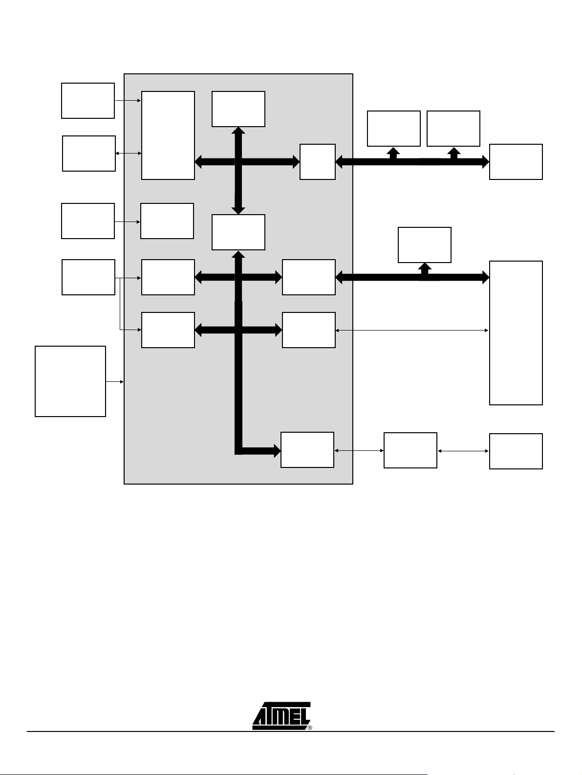
Figure 1-1. AT91EB40A Evaluation Board Block Diagram
AT91R40008
Reset
Controller
JTAG
ICE
Connector
ARM7TDMI
Processor
256K Byte
RAM
ASB
EBI
SRAM
(1)
Flash
EBI
Expansion
Connector
66 MHz
Crystal
Push-buttons
Power Supply
VDDCORE (1.8V)
VDDIO (3.3V)
Clock
Generator
Interrupt
Controller
PIO
APB
AMBA
Bridge
PIO
Timer
Counters
Serial
Ports
LEDs
RS232
Transceivers
I/O
Expansion
Connector
DB9 Serial
Connectors
Note: No external SRAM is fitted on the board. See section “Memories” on page 4-1 for more details.
AT91EB40A Evaluation Board User Guide 1-3
2635C–ATARM–13-May-05
Page 8

1-4 AT91EB40A Evaluation Board User Guide
2635C–ATARM–13-May-05
Page 9
Section 2
Setting Up the
AT91EB40A Evaluation Board
2.1 Electrostatic Warning
2.2 Requirements In order to set up the AT91EB40A evaluation board, the following requirements are
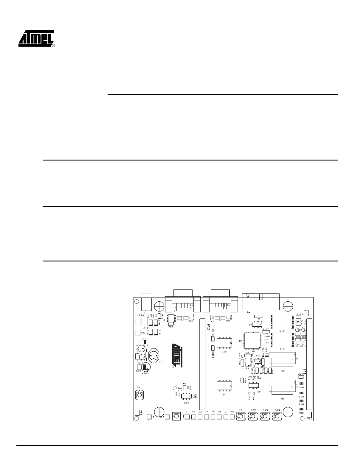
2.3 Layout Figure 2-1 shows the layout of the AT91EB40A evaluation board.
The AT91EB40A evaluation board is shipped in protective anti-static packaging. The
board must not be subjected to high electrostatic potentials. A grounding strap or similar
protective device should be worn when handling the board. Avoid touching the component pins or any other metallic element.
needed:
! The AT91EB40A evaluation board itself.
! The DC power supply capable of supplying 7V to 9V at 1A (not supplied).
Figure 2-1. Layout of the AT91EB40A Evaluation Board
AT91EB40A Evaluation Board User Guide 2-1
Rev. 2635C–ATARM–13-May-05
Page 10
2.4 Jumper Settings JP1 is used to boot standard or user programs. For standard operations, set it in the
STD position; for user programs, set it to the USER position.
CB2 is used to select the core power supply between 1.8V and 3.3V.
For more information on the CB2 setting, see “Configuration Straps” on page 5-1 in Section 5.
2.5 Powering Up the Board
2.6 Measuring Current Consumption on the AT91R40008
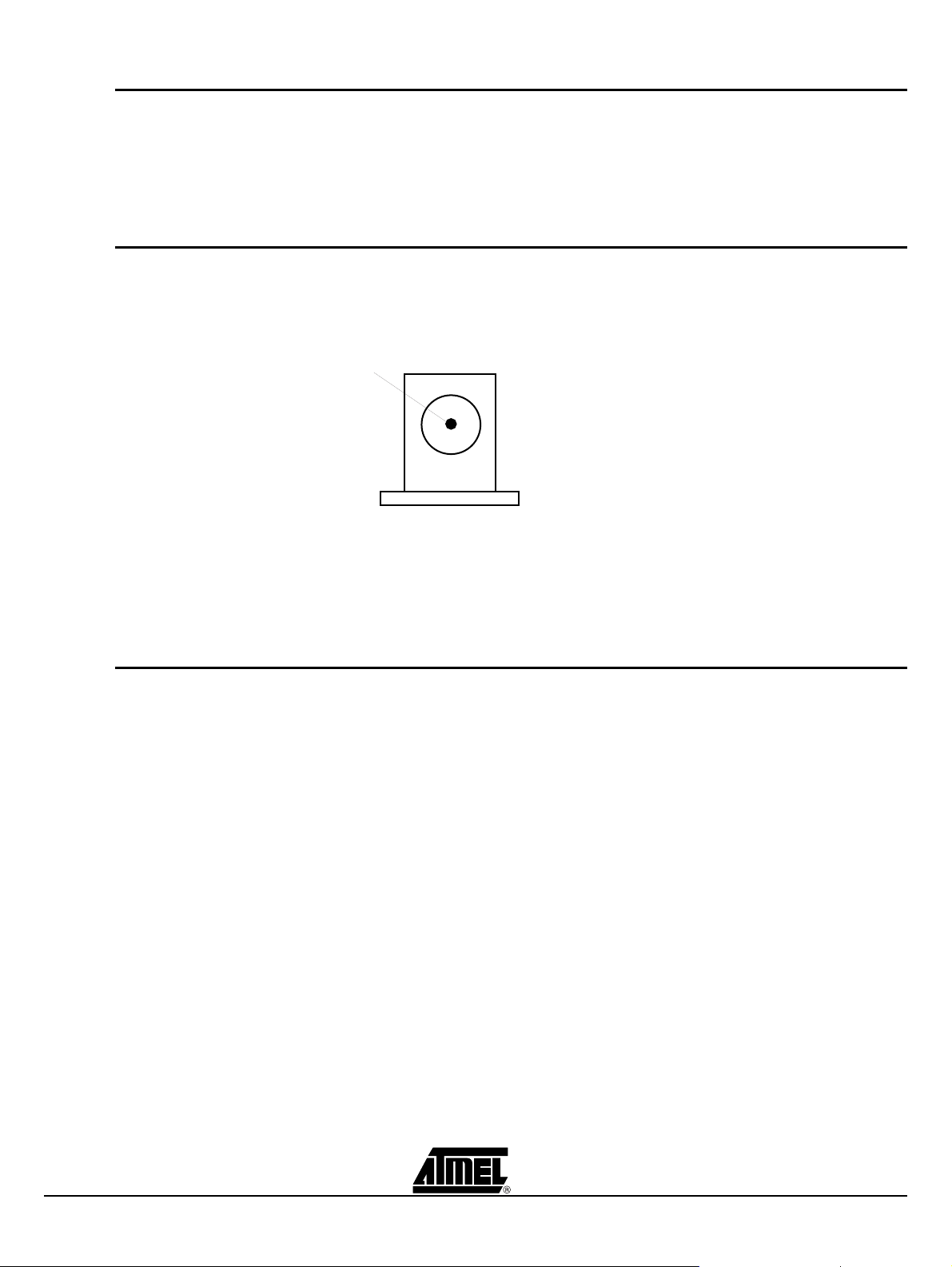
DC power is supplied to the board via the 2.1 mm socket (J1) shown in Figure 2-2. The
polarity of the power supply is not critical. The minimum voltage required is 7V.
Figure 2-2. 2.1 mm Socket
positive (+)
or
negative (-)
2.1 mm Connector
The board has a voltage regulator providing +3.3V and 1.8V. The regulator allows the
input voltage to range from 7V to 9V. When you switch the power on, the red LED D11
marked PWR lights up. If it does not, switch off and check the power supply
connections.
The board is designed to generate the power for the AT91 product, and only the AT91
product, through the jumpers JP5A/JP5B (V
ture enables the current consumption of the AT91 product to be measured.
See “Power Consumption Measurement Straps (JP5A/B, JP7A/B)” on page 5-3 in Section 5 for further details.
) and JP7A/JP7B (V
DDIO
DDCORE
). This fea-
2-2 AT91EB40A Evaluation Board User Guide
2635C–ATARM–13-May-05
Page 11

2.7 Testing the AT91EB40A Evaluation Board
To test the AT91EB40A Evaluation Board, perform the following procedure:
1. Hold down the SW1 button and power-up the board, or generate a reset and wait
for the light sequence on each LED to complete. All the LEDs light.
2. Release the SW1 button. The LEDs D1 to D5 light up in sequential order. If all
the LEDs light up twice, this indicates an error. Note that LEDs D6 to D8 are
reserved for future use.
The LEDs represent the following test functions:
! D1 for the internal SRAM
! D2 for the external SRAM
(1)
! D3 for the external Flash
! D5 for the USART
! D6 reserved
! D7 reserved
! D8 reserved
During a complete test cycle, each LED flashes once to inform the user that the corresponding function has been successfully tested. If an error is detected, all the LEDs will
light up twice. After a complete test cycle, the embedded self-test software called FTS
(Functional Test Software) restarts a new cycle.
Note: 1. At factory, no external SRAM is mounted on the board. The test shows an error. If the
user upgrades the board with external SRAM, the test runs normally.
AT91EB40A Evaluation Board User Guide 2-3
2635C–ATARM–13-May-05
Page 12

2-4 AT91EB40A Evaluation Board User Guide
2635C–ATARM–13-May-05
Page 13

Section 3
The On-board Software
3.1 The AT91EB40A Evaluation Board
3.2 Boot Software Program
The AT91EB40A Evaluation Board embeds an AT49BV1604 or AT49BV1614 Flash
memory device programmed with default software.
When delivered, the Flash memory device contains:
! the Boot Software Program
! the Functional Test Software (FTS)
! the Flash uploader
! the Angel Debug Monitor
! a default user boot with a default application (LED Swing Application)
The boot software program, functional test software (FTS), and the Flash downloader
are in sectors 0 and 1 of the Flash device. Sectors 3 to 8 support the Angel Debug Monitor. The default user boot with a default application is located in sector 24.
These sectors are not locked in order to provide an easy on-board upgrade. The user
must avoid overwriting these sectors. The remaining sectors are user definable, and can
be programmed using one of the Flash downloader "Flash_16x4" solutions offered in
the AT91 library. See “Appendix D – Flash Memory Mapping” on page 8-1 for further
details.
The boot software program configures the AT91R40008, and thus controls the memory
and other board components.
The boot software program is started at reset if JP1 is in the STD position. If JP1 is in
the USER position, the AT91R40008 boots from address 0x01100000 in the Flash,
which must have a user-defined boot.
The boot software program first initializes the EBI, then executes the REMAP procedure
and, finally, checks the state of the buttons as described below.
! When the SW1 button is pressed:
All the LEDs light up together.
The D1 LED remains lit when SW1 is released.
The Functional Test Software (FTS) is started.
! The SW2 button is reserved.
AT91EB40A Evaluation Board User Guide 3-1
Rev. 2635C–ATARM–13-May-05
Page 14

! When the SW3 button is pressed:
All the LEDs light up together.
The D3 LED remains lit when SW3 is released.
The Flash uploader is activated.
! The SW4 button is reserved for future use.
! When no buttons are pressed:
Branch at address 0x01006000.
The Angel Debug Monitor starts from this address by recopying itself in internal
SRAM.
3.3 Programmed Default Memory Mapping
Table 3-1 defines the mapping defined by the boot program.
Table 3-1. Memory Map
Part Name Start Address End Address Size Device
U1A 0x01000000 0x011FFFFF 2M Bytes
U2 - U3
Note: 1. If fitted on the board
(1)
0x02000000 0x0203FFFF 256K Bytes SRAM
Flash
AT49BV162A
U1A is divided in two parts. This is done by the jumper JP1. In the upper part, the first
sector (sector 24) at address 0x01100000 must be programmed with a boot sequence
to be debugged. This sector can be mapped at address 0x01000000 (or 0x0 after a
reset) when the jumper JP1 is in the USER position. See “Appendix A – Configuration
Straps” on page 5-1.
3.4 Flash Uploader The Flash Uploader included in the EB40A Boot software is the same Flash Uploader
factory-programmed in the Flash-based AT91 devices, the AT91FR4042 and the
AT91FR40162/S. The Flash Uploader allows programming to the Sector 24of Flash
through a serial port. Either of the on-chip USARTs can be used by the Flash Uploader.
To boot from the application downloaded in the Sector 24, the downloading address
must be 0x01100000. Other sectors in plane B can be used to store constant data. The
boot starts the Flash Uploader if the SW3 button is pressed at reset.
The procedure is as follows:
1. Connect the Serial A (or B
(1)
) port of the AT91EB40A Evaluation Board to a host
PC Serial Port using the straight serial cable provided.
2. Start the AT91Loader.exe program available in the AT91 Library on the host computer. The AT91 Loader must be configured beforehand. For more details, see
the documentation regarding the free Host Loader available for download on the
Atmel web site.
3. Check JP1 is in STD position. Power-on or press RESET, holding down the SW3
button simultaneously. Wait for all LEDs to light up together and then release
SW3. LED3 remains lit. If the AT91Loader is configured in automatic mode, the
download starts. Wait for the download to end.
3-2 AT91EB40A Evaluation Board User Guide
2635C–ATARM–13-May-05
Page 15

4. Put JP1 in USER position and press the reset button. The application downloaded starts.
Note: 1. For the Serial B port, use a female/female straight serial cable.
3.5 Angel Monitor The Angel Monitor is located in the Flash from 0x01006000 up to 0x01011FFF. The
boot program starts it if no button is pressed at reset.
When Angel starts, it recopies itself in internal SRAM in order to run faster. The internal
SRAM used by Angel is from 0x00020000 to 0x0003FFFF, i.e., the highest half part of
the internal SRAM.
The Angel on the AT91EB40A Evaluation Board can be upgraded regardless of the version programmed on it.
Note that if the debugger is started through ICE while the Angel monitor is on, the
Advanced Interrupt Controller (AIC) and the USART channel are enabled.
AT91EB40A Evaluation Board User Guide 3-3
2635C–ATARM–13-May-05
Page 16

3-4 AT91EB40A Evaluation Board User Guide
2635C–ATARM–13-May-05
Page 17

Section 4
Circuit Description
4.1 AT91R40008 Processor
4.2 Expansion Connectors
4.2.1 I/O Expansion
Connector
4.2.2 EBI Expansion
Connector
Figure 6-1 in Section 6, “Appendix B – Schematics” shows the AT91R40008. The footprint is for a 100-pin TQFP package.
Jumper JP5A/JP5B (see Figure 6-7 in Section 6, “Appendix B – Schematics”) can be
removed by the user to allow measurement of the current on V
can be removed to measure the core microcontroller consumption on V
The two expansion connectors, I/O expansion connector and EBI expansion connector,
and the JTAG interface are described below.
The I/O and EBI expansion connectors’ pinout and position are compatible with other
AT91 evaluation boards (except the I/O expansion connector pinout and position of the
EB40) so that users can connect their prototype daughter boards to any of these evaluation boards.
The I/O expansion connector P2 makes the general-purpose I/O (GPIO) lines, VCC3V3
and Ground, available to the user. Configuration straps are used to select between the
I/O lines being used by the evaluation board or by the user via the I/O expansion connector. The connector fitted at the factory is a 32 x 2 connector on a 0.1” (2.54 mm)
pitch.
The EBI expansion connector P1 makes the data bus, address bus, chip select,
read/write signals, oscillator output, wait request pins, VCC3V3 and Ground available to
the user. The connector fitted at the factory is a 32 x 2 connector on a 0.1” (2.54 mm)
pitch.
. Jumper JP7A/JP7B
DDIO
DDCORE
.
4.3 Memories The schematic (Figure 6-2 on page 6-3 in Section 6, “Appendix B – Schematics”) shows
two 128K/512K x 8 SRAM devices that can be added to the AT91EB40A.
Note: The AT91EB40A evaluation board does not feature any external SRAM. The
user can add SRAM ranging in size from 256K bytes x 16 bits to 1M byte x 16
bits. See “Increasing Memory Size” on page 5-4 for SRAM references.
Figure 6-8 on page 6-9 shows the Flash memories. The printed circuit board of the
EB40A provides two footprints (U1A and U1B) for two different Flash memories. At factory, the EB40A fits an AT49BV162A Flash memory (U1A). U1A footprint can also
accept an AT49BV161 Flash memory. An extra Flash memory can be added on U1B
footprint. The U1B footprint can accept an AT49BV8011 or an AT49BV400 Flash memory. The Flash memory on U1A and the Flash memory on U1B cannot be used at the
AT91EB40A Evaluation Board User Guide 4-1
Rev. 2635C–ATARM–13-May-05
Page 18

same time (i.e., one as a boot memory and the other as data storage memory). In fact,
the AT91 NCS0 chip select line is connected to U1A or U1B chip select line according to
the position of CB11. See “Appendix A – Configuration Straps” and Figure 6-8 in
“Appendix B – Schematics” .
4.4 Power and Crystal Quartz
The system clock is derived from a single 66 MHz crystal oscillator. An external clock
can be input on the EB40A via the EBI connector on pin B4 - EBI_MCKI. See Figure 6-6
in “Appendix B – Schematics” .
The voltage regulator U9 provides 3.3V to VDDIO and to all other devices of the board.
The voltage regulator U11 provides 1.8V for VDDCORE of the AT91R40008.
Power can be applied via the 2.1mm connector to the regulator in either polarity
because of the diode-rectifying circuit.
4.5 Push-buttons, LEDs and Serial Interfaces
4.5.1 Push-buttons and
LEDs
4.5.2 Serial Interface Two 9-way D-type connectors (P3/P4) are provided for serial port connection.
Figure 6-3 in “Appendix B – Schematics” shows push buttons and LEDs. SW1, SW2,
SW3 and SW4 push buttons are debounced, buffered and connected to P12/FIQ,
P9/IRQ0, P1/TIOA0 and P2/TIOB0, respectively. The eight general-purpose LEDs are
connected to PIO (P15 to P19 and P3 to P6).
Serial port A (P3) is used primarily for Host PC communication and is a DB9 female connector. TXD and RXD are swapped, so that a straight-through cable can be used. CTS
and RTS are connected together, as is DCD, DSR and DTR.
Serial port B (P4) is a DB9 male connector with TXD and RXD in conformance with the
standard RS-232 pinout. Apart from TXD, RXD and ground, the other pins are not
connected.
A MAX3223 device (U10) and associated bulk storage capacitors provide RS-232 level
conversion.
4.6 Reset Circuit and JTAG Interface
4.6.1 Reset Circuit A supervisory circuit has been included in the design to detect and consequently reset
the board when the 3.3V supply voltage drops below 2.7V. Note that this voltage can be
changed depending on the board production series. The supervisory circuit also provides a debounced reset signal. This device also generates the reset signal in case of
watchdog timeout, as the pin NWDOVF of the AT91R40008 is connected on its input
/MR.
The assertion of this reset signal lights the red RESET LED (D10). By pressing the
CLEAR RESET push button (S2), the LED is turned off.
4-2 AT91EB40A Evaluation Board User Guide
2635C–ATARM–13-May-05
Page 19

4.6.2 JTAG Interface An ARM-standard 20-pin box header (P5) is provided to enable connection of an ICE to
the JTAG inputs on the AT91. This allows code to be debugged on the board without
using system resources, such as memory and serial ports.
4.7 Layout Drawing The layout diagram (Figure 6-1 on page 6-2 in Section 6, “Appendix B – Schematics”)
shows an approximate floorplan for the board. This has been designed to give the lowest board area, while still providing access to all test points, jumpers and switches on
the board.
The board is provided with four mounting holes, one at each corner, into which feet are
attached. The board has two signal layers and two power planes.
AT91EB40A Evaluation Board User Guide 4-3
2635C–ATARM–13-May-05
Page 20

4-4 AT91EB40A Evaluation Board User Guide
2635C–ATARM–13-May-05
Page 21

Section 5
Appendix A – Configuration Straps
5.1 Configuration Straps
By using the I/O and EBI expansion connectors, users can connect their own peripherals to the evaluation board. These peripherals may require more I/O lines than available
while the board is in its default state. Extra I/O lines can be made available by disabling
some of the on-board peripherals or features. This is done using the configuration straps
detailed below. Some of these straps present a default wire (notified by the default mention) that must be cut before soldering the strap.
CB1 On-board CS4 Signal
(1)
Closed
Open AT91 CS4 signal is not connected to the EBI expansion connector (P1-B21).
(2)
CB2
1 - 2 The AT91 core is powered by 3.3V power supply. NOT ALLOWED for the
2 - 3 The AT91 core is powered by 1.8V power supply.
AT91 CS4 signal is connected to the EBI expansion connector
(P1-B21).
This authorizes users to connect the EBI expansion connector of this board
to the MPI expansion connector of an AT91EB63 Evaluation Board without
conflict problems.
Core Power Supply Selection
AT91R40008.
CB3 On-board Boot Chip Select
(1)
Closed
Open AT91 NCS0 select signal is not connected to the Flash memory. This
AT91EB40A Evaluation Board User Guide 5-1
AT91 NCS0 select signal is connected to the Flash memory (U1A or U1B).
See also CB11.
authorizes users to connect the corresponding chip select signal to their own
resources via the EBI Expansion Connector.
Rev. 2635C–ATARM–13-May-05
Page 22

CB4 Flash Reset (U1A)
Closed
(1)
The on-board reset signal NRST is connected to the Flash NRESET input.
Open The on-board reset signal NRST is not connected to the Flash NRESET
input.
CB5 Flash RDY/BUSY Pin (U1A)
(1)
Closed
The RDY/BUSY line of the Flash memory is connected to P10/IRQ1 pin.
Open The RDY/BUSY line of the Flash memory is not connected to P10/IRQ1 pin.
CB6 Push-button Enabling
(1)
Open
Closed SW1 to SW4 inputs to the AT91 are not valid. This authorizes users to
CB9 AT91 Master Clock Input
1 - 2 AT91 Master Clock input (MCKI) is connected to the on-board 66 MHz
2 - 3 AT91 Master Clock input (MCKI) is connected to the EBI_MCKI (B4) pin of
SW1 to SW4 inputs to the AT91 are valid.
connect the corresponding PIO to their own resources via the I/O Expansion
Connector.
oscillator.
the EBI expansion connector. This authorizes the user to input an external
clock to the AT91.
CB10 Ground Link
Closed The electrical ground is connected to mechanical ground.
Open
(1)
The electrical ground is not connected to mechanical ground.
CB11 On-board Flash Memory Selection
1 -2 AT91 NCS0 select signal is connected to the Flash device U1A.
2 - 3 AT91 NCS0 select signal is connected to the Flash device U1B.
CB12 Flash Reset (U1B)
(1)
Closed
Open The on-board reset signal is not connected to the Flash NRESET input.
CB15 Flash RDY/BUSY Pin (U1B)
(1)
Closed
Open The RDY/BUSY line of the Flash memory is not connected to P10/IRQ1 pin.
The on-board reset signal is connected to the Flash NRESET input.
The RDY/BUSY line of the Flash memory is connected to P10/IRQ1 pin.
5-2 AT91EB40A Evaluation Board User Guide
2635C–ATARM–13-May-05
Page 23

CB16 Highest Address Bit
(1)
Open
Closed Setting to support an AT49BV1604/A on U1A footprint.
JP1 User or Standard Boot Selection
2-3 The first half of the Flash memory is accessible at its base address.
1-2 The second half of the Flash memory is accessible at its base address. This
Notes: 1. Hardwired default position: To cancel this default configuration, the user should first
2. Regarding CB2 setting: The EB40A also supports an AT91M40800 or an
Setting to support an AT49BV1604 or AT49BV1614 (or an AT49BV161) on
U1A footprint or an AT49BV8011 (or an AT49BV400) on U1B footprint.
authorizes users to download their own application software in this part and
to boot on it.
cut the wire on the board.
AT91R40807. However, if the user wants to evaluate these devices, the microcontroller U7 and the oscillator Y1 must be changed. If an AT91M40800 is mounted on the
board, external SRAM must be added to increase SRAM quantity since the
AT91M40800 embeds 8K bytes only.
To upgrade the EB40A to support an AT91M40800 or an AT91R40807:
1. De-solder the microcontroller U7.
2. Solder the AT91M40800 or the AT91R40807 to the U7 footprint.
3. De-solder the crystal oscillator Y1.
4. Solder a crystal oscillator (up to 40 MHz) to the Y1 footprint.
5. Set CB2 to 1 - 2 before supplying the board.
5.2 Power Consumption Measurement Straps (JP5A/B, JP7A/B)
5.3 Ground Links (JP6)
The JP5A/B straps enable connection of an ammeter to measure the AT91R40008 global consumption on VDDIO.
The JP7A/B straps enable connection of an ammeter to measure the AT91R40008 global consumption on VDDCORE.
The CB10 strap allows the user to connect the electrical and mechanical grounds.
AT91EB40A Evaluation Board User Guide 5-3
2635C–ATARM–13-May-05
Page 24

5.4 Increasing Memory Size
The AT91EB40A Evaluation Board is not supplied with external SRAM devices. If, however, the user needs more than 256K bytes of internal memory embedded in the
AT91R40008, SRAM from 256K bytes to 1M bytes may be added.
The following references for the 128K x 8 SRAM are available:
Manufacturer Reference
Samsung U2 - U3 footprint: KM68V1002BJ-10 in 32-SOJ-400 package
U4 - U5 footprint: KM68V1002BJ-10 in 32-TSOP2-400F package
IDT U2 - U3 footprint: 71V124-S10Y in 400-mil SOJ package (SO32-3)
U4 - U5 footprint: 71V124-S10PH in TSOP Type II (SO32-4)
The following references for the 512K x 8 SRAM are available:
Manufacturer Reference
Samsung U2 - U3 footprint: KM68V4002BJ-10 in 36-SOJ-400 package
U4 - U5 footprint: KM68V4002BJ-10 in 36-TSOP2-400F package
IDT U2 - U3 footprint: 71V424-S10Y in 36-pin 400-mil SOJ package
U4 - U5 footprint: 71V124-S10PH in 44-pin TSOP Type II
5-4 AT91EB40A Evaluation Board User Guide
2635C–ATARM–13-May-05
Page 25

Appendix B – Schematics
6.1 Schematics The following schematics are appended:
! Figure 6-1. PCB Layout
! Figure 6-2. SRAM Memory Devices and Two-wire Interface Memory
! Figure 6-3. Push Buttons, LEDs and Serial Interface
! Figure 6-4. Reset and JTAG Interface
! Figure 6-5. AT91R40008
! Figure 6-6. I/O and EBI Expansion Connectors
! Figure 6-7. Power Supply
! Figure 6-8. Flash Memory Devices
Section 6
The pin connectors are indicated on the schematics:
! P1 = EBI Expansion Connector (Figure 6-6)
! P2 = I/O Expansion Connector (Figure 6-6)
! P3 = Serial A (Figure 6-3)
! P4 = Serial B (Figure 6-3)
! P5 = JTAG Interface (Figure 6-4)
AT91EB40A Evaluation Board User Guide 6-1
Rev. 2635C–ATARM–13-May-05
Page 26

Figure 6-1. PCB Layout
6-2 AT91EB40A Evaluation Board User Guide
2635C–ATARM–13-May-05
Page 27

Figure 6-2. SRAM Memory Devices and Two-wire Interface Memory
Not mounted
AT91EB40A Evaluation Board User Guide 6-3
2635C–ATARM–13-May-05
Page 28

Figure 6-3. Push Buttons, LEDs and Serial Interface
6-4 AT91EB40A Evaluation Board User Guide
2635C–ATARM–13-May-05
Page 29

Figure 6-4. Reset and JTAG Interfaces
JTAG Connector (Front View)
1
3
5
7
9
11
13
15
17
19
2
4
6
8
10
12
14
16
18
20
AT91EB40A Evaluation Board User Guide 6-5
2635C–ATARM–13-May-05
Page 30

Figure 6-5. AT91R40008
6-6 AT91EB40A Evaluation Board User Guide
2635C–ATARM–13-May-05
Page 31

Figure 6-6. I/O and EBI Expansion Connectors
AT91EB40A Evaluation Board User Guide 6-7
2635C–ATARM–13-May-05
Page 32

Figure 6-7. Power Supply
6-8 AT91EB40A Evaluation Board User Guide
2635C–ATARM–13-May-05
Page 33

Figure 6-8. Flash Memory Devices
VPP
AT49BV162A
AT91EB40A Evaluation Board User Guide 6-9
2635C–ATARM–13-May-05
Page 34

6-10 AT91EB40A Evaluation Board User Guide
2635C–ATARM–13-May-05
Page 35

Section 7
Appendix C – Bill of Materials
Table 7-1. Bill of Materials for AT91EB40A
Item Qty Reference Part Designation Manufacturer
1 14 R6 to R13, R23, R24, R104,
R105, R107, R108
100 Ohm Resistor 5%
2 27 R3 to R5, R14 to R17, R22,
R25, R31, R42 to R45, R51,
R54, R101 to R103, R106,
R109 to R115
3 4 R1, R2, R18, R100 Footprint, resistor
4 6 C78 to C81, C84, C85 10 pF Ceramic Capacitor X7R/10V
5 8 C20, C21, C23, C24, C26,
C27, C55, C59
6 9 C7, C8, C9, C38 to C43 47 pF Ceramic Capacitor X7R/10V
7 1 C60 3.3 nF Ceramic Capacitor X7R/10V
8 11 C25, C71 to C77, C82, C83,
C86,
9 4 C10, C11, C14, C15 47 nF Ceramic Capacitor X7R/10V
10 28 C1 to C6, C12, C13, C16 to
C19, C22, C28 to C37, C52
to C54, C67, C95
11 3 C61, C62, C64 1 µF Ceramic Capacitor
12 1 C63 10 µF Capacitor 16V SMT AVX
13 1 C57 10 µF Capacitor 25V SMT AVX
14 1 C57B 10 µF Capacitor 25V-Radial D -CO37
100k Ohm Resistor 5%
22 pF Ceramic Capacitor X7R/10V
10 nF Ceramic Capacitor X7R/10V
100 nF Ceramic Capacitor X7R/10V
15 1 C58 100 µF Capacitor 100µF/10V SMT AVX AVX
16 1 C58B 100 µF Capacitor 100µF/10V Radial AVX
C-C037
18 2 JP5A, JP5B, JP7A, JP7B 2 point Jumper 2 point, step 2.54 mm
20 1 JP1 3 point Jumper 3 point, step 2.54 mm
21 2 P1, P2 2x32 point Male, step 2.54 mm
22 2 JP5A, JP5B, JP7A, JP7B 2 point by step 2.54 mm
AT91EB40A Evaluation Board User Guide 7-1
Rev. 2635C–ATARM–13-May-05
Page 36

Table 7-1. Bill of Materials for AT91EB40A (Continued)
Item Qty Reference Part Designation Manufacturer
23 1 J1 Jack Diameter 2.1 mm Jack Socket Æ 2.1mm
24 4 TP1, TP2, TP3, TP4 Test Point Corner SMT Test Point 2.7 x 3.9
25 1 P3 Sub D 9b F Sub D 9b Female socket, right
angle, mechanical strength,
locking
26 1 P4 Sub D 9b M Sub D 9b Male socket, right angle,
mechanical strength, locking
27 1 P5 HE10 2x10 HE10 2 x 10 socket, low profile,
right angle
28 1 D9 D-BAS32L Diode Signal Philips
29 4 D16 to D19 10MQ100N Rectifier Diode I.R.
30 1 D15 1N5817 Schottky Diode 1A/0.45V Fairchild
31 1 D12 1N914 Diode Fairchild
32 1 D14 SMT6T15CA Transil 12.8V / 600W / VBRmini
14.3V
33 10 D1 to D8, D10, D11, LED SMT LED, Red color
34 2 D22, D23 LED SMT LED, Green color
35 2 D20, D21 LED SMT LED, Yellow color
AMP
36 1 F1 POLYSWITCH Fuse RARM 1000 mA/30V
37 1 L1 10 µH Self 10 µH at 1A and 500kHz
38 6 SW1 to SW5, S2 Push Button Push Button KSA
39 1 Y1 66 MHz Oscillator 3.3V SMT Crystal Oscillator
Koni
HCMOS, K3750 HCE
40 1 U9 74LV125D Buffer Tri-state
41 1 U8 74LV244D Buffer
42 1 U6 74LV04AD Inverters
43 1 U16 74LV74AD Dual D Type Flip Flop
45 2 U1A AT49BV162A-70TI 16-megabit Flash Memory Atmel
46 1 U7 AT91R40008 32bit ARM/Thumb Microcontroller Atmel
47 2 U2, U3 IDT71V424S10Y SRAM IDT
48 1 U11 LT1503CS8-1.8 Regulator DC/DC Linear Tech.
49 1 U19 LT1507CS8-3.3 Regulator DC/DC Linear Tech.
50 1 U10 MAX3223ECAP RS232 Driver Maxim
51 1 U17 MAX6315US27D1-T Power Supply Supervisor (2.7V
Maxim
Threshold Voltage)
52 4 PS1, PS2, PS3, PS4 Board Support Plastic bases H>10 mm
7-2 AT91EB40A Evaluation Board User Guide
2635C–ATARM–13-May-05
Page 37

Section 8
Appendix D – Flash
Memory Mapping
Figure 8-1 shows the embedded software mapping after the remap. It describes the
location of the different programs in the AT49BV162A Flash memory and the division
into sectors.
Figure 8-1. EB40A Flash Memory Software Mapping
0x011FFFFF
Not Used
15 Sectors
(64K Bytes/Sector)
1 MB
User Mode
0x01100000
0x01012000
0x01011FFF
0x01006000
0x01005FFF
0x01004000
0x01000000
LED Swing Application
(Example)
Not Used
Not Used
Angel Debug
Monitor
Free Sector for
Boot Upgrade
Flash Uploader
Functional Test Software
Boot Program
15 Sectors
(64K Bytes/Sector)
1 Sector
(64K Bytes/Sector) +
5 Sectors
(8K Bytes/Sector)
1 Sector
(8K Bytes/Sector)
2 Sectors
(8K Bytes/Sector)
1 MB
Standard
Mode
AT91EB40A Evaluation Board User Guide 8-1
Rev. 2635C–ATARM–13-May-05
Page 38

8-2 AT91EB40A Evaluation Board User Guide
2635C–ATARM–13-May-05
Page 39

Document Details
Title AT91EB40A Evaluation Board User Guide
Literature Number 2635
Revision History
Version A Publication Date: Mar-02
Version B Publication Date: 21-Jun-02
Revisions since last issue
Page: 3-2, 3-3 Change in compilation address in SRAM Downloader
Version C Publication Date: 13-May-05
Revisions since last issue
Section 1.3 Removed "64K bytes of EEPROM"
Fig.1-1 Removed the Two-wire Interface" box
Section 2.7 Removed "D4 for the EEPROM with two-wire interface access"
Section 3.2 Removed all references to "SRAM Downloader"
Replaced the description of "When SW2 button is pressed" by Reserved
Section 3.4 Removed
Section 3.5 Replaced AT91F40816 and AT91FR4081 by AT91FR4042 and AT91FR4162/S
Section 4.3 Removed "AT24C512 64Kb TWI EEPROM"
Changed "AT49BV1604 or AT49BV1614" to "AT49BV162A
Section 5.1 Removed the table describing CB13, CB14
Figure 6-2 Removed the U23 part.
Figure 6-8 For U1A part: changed AT49BV1614 to AT40BV162A
Appendix C Removed item 44
Item 45 / "Part" Column --> changed to AT49BV162A-70TI
Appendix D Changed AT49BV1604 and AT49BV1614 to AT49BV162A
Figure 8-1 Updated with new Flash memory ranges
2635C–ATARM–13-May-05
1
Page 40

Atmel Corporation Atmel Operations
2325 Orchard Parkway
San Jose, CA 95131, USA
Tel: 1(408) 441-0311
Fax: 1(408) 487-2600
Regional Headquarters
Europe
Atmel Sarl
Route des Arsenaux 41
Case Postale 80
CH-1705 Fribourg
Switzerland
Tel: (41) 26-426-5555
Fax: (41) 26-426-5500
Asia
Room 1219
Chinachem Golden Plaza
77 Mody Road Tsimshatsui
East Kowloon
Hong Kong
Tel: (852) 2721-9778
Fax: (852) 2722-1369
Japan
9F, Tonetsu Shinkawa Bldg.
1-24-8 Shinkawa
Chuo-ku, Tokyo 104-0033
Japan
Tel: (81) 3-3523-3551
Fax: (81) 3-3523-7581
Memory
2325 Orchard Parkway
San Jose, CA 95131, USA
Tel: 1(408) 441-0311
Fax: 1(408) 436-4314
Microcontrollers
2325 Orchard Parkway
San Jose, CA 95131, USA
Tel: 1(408) 441-0311
Fax: 1(408) 436-4314
La Chantrerie
BP 70602
44306 Nantes Cedex 3, France
Tel: (33) 2-40-18-18-18
Fax: (33) 2-40-18-19-60
ASIC/ASSP/Smart Cards
Zone Industrielle
13106 Rousset Cedex, France
Tel: (33) 4-42-53-60-00
Fax: (33) 4-42-53-60-01
1150 East Cheyenne Mtn. Blvd.
Colorado Springs, CO 80906, USA
Tel: 1(719) 576-3300
Fax: 1(719) 540-1759
Scottish Enterprise Technology Park
Maxwell Building
East Kilbride G75 0QR, Scotland
Tel: (44) 1355-803-000
Fax: (44) 1355-242-743
RF/Automotive
Theresienstrasse 2
Postfach 3535
74025 Heilbronn, Germany
Tel: (49) 71-31-67-0
Fax: (49) 71-31-67-2340
1150 East Cheyenne Mtn. Blvd.
Colorado Springs, CO 80906, USA
Tel: 1(719) 576-3300
Fax: 1(719) 540-1759
Biometrics/Imaging/Hi-Rel MPU/
High Speed Converters/RF Datacom
Avenue de Rochepleine
BP 123
38521 Saint-Egreve Cedex, France
Tel: (33) 4-76-58-30-00
Fax: (33) 4-76-58-34-80
Literature Requests
www.atmel.com/literature
Disclaimer: The information in this document is provided in connection with Atmel products. No license, express or implied, by estoppel or otherwise, to any
intellectual property right is granted by this document or in connection with the sale of Atmel products. EXCEPT AS SET FORTH IN ATMEL’S TERMS AND CONDI-
TIONS OF SALE LOCATED ON ATMEL’S WEB SITE, ATMEL ASSUMES NO LIABILITY WHATSOEVER AND DISCLAIMS ANY EXPRESS, IMPLIED OR STATUTORY
WARRANTY RELATING TO ITS PRODUCTS INCLUDING, BUT NOT LIMITED TO, THE IMPLIED WARRANTY OF MERCHANTABILITY, FITNESS FOR A PARTICULAR
PURPOSE, OR NON-INFRINGEMENT. IN NO EVENT SHALL ATMEL BE LIABLE FOR ANY DIRECT, INDIRECT, CONSEQUENTIAL, PUNITIVE, SPECIAL OR INCIDENTAL DAMAGES (INCLUDING, WITHOUT LIMITATION, DAMAGES FOR LOSS OF PROFITS, BUSINESS INTERRUPTION, OR LOSS OF INFORMATION) ARISING OUT
OF THE USE OR INABILITY TO USE THIS DOCUMENT, EVEN IF ATMEL HAS BEEN ADVISED OF THE POSSIBILITY OF SUCH DAMAGES. Atmel makes no
representations or warranties with respect to the accuracy or completeness of the contents of this document and reserves the right to make changes to specifications
and product descriptions at any time without notice. Atmel does not make any commitment to update the information contained herein. Atmel’s products are not
intended, authorized, or warranted for use as components in applications intended to support or sustain life.
© Atmel Corporation 2005. All rights reserved. Atmel®, logo and combinations thereof, Everywhere You Are® and others are registered trade-
marks, and others are the trademarks of Atmel Corporation or its subsidiaries. Other terms and product names may be trademarks of others.
Printed on recycled paper.
2635C–ATARM–13-May-05
Page 41

Mouser Electronics
Authorized Distributor
Click to View Pricing, Inventory, Delivery & Lifecycle Information:
Microchip:
AT91EB40A
 Loading...