

Page 1
BDTIC www.bdtic.com/ATMEL
Features
• High Performance, Low Power AVR
• Advanced RISC Architecture
– 135 Powe rful Instructions – Most Single Clock Cy cle Execution
– 32 x 8 General Purpose Working Registers
– Fully Static Operation
– Up to 16 MIPS Throughput at 16 MHz
– On-Chip 2-cycle Multiplier
• Non-volatile Program and Data Memories
– 32/64/128K Bytes of In-System Self-Programmable Flash
• Endurance: 100,000 Write/Erase Cycles
– Optional Boot Code Section with Independent Lock Bits
• USB Bootloader programmed by default in the Factory
• In-System Programming by On-chip Boot Program hardware activated after
reset
• True Read-While-Write Operation
• All supplied parts are preprogramed with a default USB bootloader
– 1K/2K/4K (32K/64K/128K Flash version) Bytes EEPROM
• Endurance: 100,000 Write/Erase Cycles
– 2.5K/4K/8K (32K/64K/128K Flash version) Bytes Internal SRAM
– Up to 64K Bytes Optional External Memory Space
– Programming Lock for Software Security
• JTAG (IEEE std. 1149.1 compliant) Interface
– Boundary-scan Capabilities According to the JTAG Standard
– Extensive On-chip Debug Support
– Programming of Flash, EEPROM, Fuses, and Lock Bits through the JTAG Interface
• USB 2.0 Full-speed/Low-speed Device and On-The-Go Module
– Complies fully with:
– Universal Serial Bus Specification REV 2.0
– On-The-Go Supplement to the USB 2.0 Specification Rev 1.0
– Supports data transfer rates up to 12 Mbit/s and 1.5 Mbit/s
• USB Full-speed/Low Speed Device Module with Interrupt on Transfer Completion
– Endpoint 0 for Control Transfers : up to 64-bytes
– 6 Programmable Endpoints with IN or Out Directions and with Bulk, Interrupt or
Isochronous Transfers
– Configurable Endpoints size up to 256 bytes in double bank mode
– Fully independant 832 bytes USB DPRAM for endpoint memory allocation
– Suspend/Resume Interrupts
– Power-on Reset and USB Bus Reset
– 48 MHz PLL for Full-speed Bus Operation
– USB Bus Disconnection on Microcontroller Request
• USB OTG Reduced Host :
– Supports Host Negotiation Protocol (HNP) and Session Request Protocol (SRP)
for OTG dual-role devices
– Provide Status and control signals for software implementation of HNP and SRP
– Provides programmable times required for HNP and SRP
• Peripheral Features
– Two 8-bit Timer/Counters with Separate Prescaler and Compare Mode
– Two16-bit Timer/Counter with Separate Prescaler, Compare- and Capture Mode
®
8-Bit Microcontroller
8-bit
Microcontroller
with
64/128K Bytes
of ISP Flash
and USB
Controller
ATmega32U6*
AT90USB646
AT90USB647
AT90USB1286
AT90USB1287
*Preliminary
Summary
7593IS–AVR–02/09
Page 2

ATmega32U6/AT90USB64/128
– Real Time Counter with Separate Oscillator
– Four 8-bit PWM Channels
– Six PWM Channels with Programmable Resolution from 2 to 16 Bits
– Output Compare Modulator
– 8-channels, 10-bit ADC
– Programmable Serial USART
– Master/Slave SPI Serial Interface
– Byte Oriented 2-wire Serial Interface
– Programmable Watchdog Timer with Separate On-chip Oscillator
– On-chip Analog Comparator
– Interrupt and Wake-up on Pin Change
• Special Microcontroller Features
– Power -on Reset and Programmable Brown-out Detection
– Internal Calibrated Oscillator
– External and Internal Interrupt Sources
– Six Sleep Modes: Idle, ADC Noise Reduction, Power-save, Power-down, Standby, and Extended Standby
• I/O and Pac kages
– 48 Programmable I/O Lines
– 64-lead TQFP and 64-lead QFN
• Operating Voltages
– 2.7 - 5.5V
• Operating temperature
– Industrial (-40°C to +85°C)
• Maximum Frequency
– 8 MHz at 2.7V - Industrial range
– 16 MHz at 4.5V - Industrial range
2
7593IS–AVR–02/09
Page 3
1. Pin Configurations
ATmega32U6
AT90USB90128/64
TQFP64
(INT.7/AIN.1/UVcon) PE7
UVcc
D-
D+
UGnd
UCap
VBus
(IUID) PE3
(SS/PCINT0) PB0
(INT.6/AIN.0) PE6
(PCINT1/SCLK) PB1
(PDI/PCINT2/MOSI) PB2
(PDO/PCINT3/MISO) PB3
(PCINT4/OC.2A) PB4
(PCINT5/OC.1A) PB5
(PCINT6/OC.1B) PB6
(PCINT7/OC.0A/OC.1C) PB7
(INT4/TOSC1) PE4
(INT.5/TOSC2) PE5
RESET
VCC
GND
XTAL2
XTAL1
(OC0B/SCL/INT0) PD0
(OC2B/SDA/INT1) PD1
(RXD1/INT2) PD2
(TXD1/INT3) PD3
(ICP1) PD4
(XCK1) PD5
PA3 (AD3)
PA4 (AD4)
PA5 (AD5)
PA6 (AD6)
PA7 (AD7)
PE2 (ALE/HWB)
PC7 (A15/IC.3/CLKO)
PC6 (A14/OC.3A)
PC5 (A13/OC.3B)
PC4 (A12/OC.3C)
PC3 (A11/T.3)
PC2 (A10)
PC1 (A9)
PC0 (A8)
PE1 (RD)
PE0 (WR)
AVCC
GND
AREF
PF0 (ADC0)
PF1 (ADC1)
PF2 (ADC2)
PF3 (ADC3)
PF4 (ADC4/TCK)
PF5 (ADC5/TMS)
PF6 (ADC6/TDO)
PF7 (ADC7/TDI)
GND
VCC
PA0 (AD0)
PA1 (AD1)
PA2 (AD2)
(T1) PD6
(T0) PD7
INDEX CORNER
1
2
3
4
5
6
7
8
9
10
11
12
13
14
15
16
64
63
62
61
60
59
58
57
56
55
54
53
52
51
50
49
48
47
46
45
44
43
42
41
40
39
38
37
36
35
34
33
17
18
19
20
21
22
23
24
25
26
27
28
29
30
31
32
Figure 1-1. Pinout ATmega32U6/AT90USB64/128-TQFP
ATmega32U6/AT90USB64/128
7593IS–AVR–02/09
3
Page 4
ATmega32U6/AT90USB64/128
Figure 1-2. Pinout ATmega32U6/AT90USB64/128-QFN
2
3
1
4
5
6
7
8
9
10
11
12
13
14
16 33
15
47
46
48
45
44
43
42
41
40
39
38
37
36
35
34
17
182019
21222324252627
29
28
32
31
30
525150
49
6463625361
60
59
58
57
56
55
54
ATmega32U6
AT90USB128/64
(64-lead QFN top view)
INDEX CORNER
AVCC
GND
AREF
PF0 (ADC0)
PF1 (ADC1)
PF2 (ADC2)
PF3 (ADC3)
PF4 (ADC4/TCK)
PF5 (ADC5/TMS)
PF6 (ADC6/TDO)
PF7 (ADC7/TDI)
GND
VCC
PA0 (AD0)
PA1 (AD1)
PA2 (AD2)
(INT.7/AIN.1/UVcon) PE7
UVcc
D-
D+
UGnd
UCap
VBus
(IUID) PE3
(SS/PCINT0) PB0
(INT.6/AIN.0) PE6
(PCINT1/SCLK) PB1
(PDI/PCINT2/MOSI) PB2
(PDO/PCINT3/MISO) PB3
(PCINT4/OC.2A) PB4
(PCINT5/OC.1A) PB5
(PCINT6/OC.1B) PB6
(INT4/TOSC1) PE4
(INT.5/TOSC2) PE5
VCC
GND
XTAL2
XTAL1
(OC0B/SCL/INT0) PD0
(OC2B/SDA/INT1) PD1
(RXD1/INT2) PD2
(TXD1/INT3) PD3
(ICP1) PD4
(XCK1) PD5
(T1) PD6
(T0) PD7
RESET
PA3 (AD3)
PA4 (AD4)
PA5 (AD5)
PA6 (AD6)
PA7 (AD7)
PE2 (ALE/HWB)
PC7 (A15/IC.3/CLKO)
PC6 (A14/OC.3A)
PC5 (A13/OC.3B)
PC4 (A12/OC.3C)
PC3 (A11/T.3)
PC2 (A10)
PC1 (A9)
PC0 (A8)
PE1 (RD)
PE0 (WR)
1.1 Disclaimer
2. Overview
Note: The large center pad underneath the MLF packages is made of metal and internally connected to
GND. It should be soldered or glued to the board to ensure good mechanical stability. If the center
pad is left unconnected, the package might loosen from the board.
Typical values contained in this datasheet are based on simulations and characterization of
other AVR microcontrollers manufactured o n th e same proce ss te ch nolo gy. Min a nd Ma x valu es
will be available after the device is characterized.
The ATmega32U6/AT90USB64/128 is a low-power CMOS 8-bit microcontroller based on the
AVR enhanced RISC architecture. By executing powerful instructions in a single clock cycle, the
4
7593IS–AVR–02/09
Page 5
ATmega32U6/AT90USB64/128 achieves throughputs approaching 1 MIPS per MHz allowing
PROGRAM
COUNTER
ST ACK
POINTER
PROGRAM
FLASH
MCU CONTROL
REGISTER
SRAM
GENERAL
PURPOSE
REGISTERS
INSTRUCTION
REGISTER
TIMER/
COUNTERS
INSTRUCTION
DECODER
DATA DIR.
REG. PORTB
DATA DIR.
REG. PORTE
DATA DIR.
REG. PORT A
DATA DIR.
REG. PORTD
DATA REGISTER
PORTB
DATA REGISTER
PORTE
DATA REGISTER
PORT A
DATA REGISTER
PORTD
INTERRUPT
UNIT
EEPROM
SPIUSART1
ST ATUS
REGISTER
Z
Y
X
ALU
POR TB DRIVERS
POR TE DRIVERS
POR TA DRIVERS
POR TF DRIVERS
POR TD DRIVERS
POR TC DRIVERS
PB7 - PB0PE7 - PE0
PA7 - P A0PF7 - PF0
RESET
VCC
AGND
GND
AREF
XT AL1
XT AL2
CONTROL
LINES
+
-
ANALOG
COMP ARATOR
PC7 - PC0
INTERNAL
OSCILLA TOR
WATCHDOG
TIMER
8-BIT DA TA BUS
AVCC
USB
TIMING AND
CONTROL
OSCILLA TOR
CALIB. OSC
DATA DIR.
REG. PORT C
DATA REGISTER
PORT C
ON-CHIP DEBUG
JTAG TAP
PROGRAMMING
LOGIC
BOUNDARY-
SCAN
DATA DIR.
REG. PORT F
DATA REGISTER
PORT F
ADC
POR - BOD
RESET
PD7 - PD0
TWO-WIRE SERIAL
INTERFACE
PLL
the system designer to optimize power consumption versus processing speed.
2.1 Block Diagram
Figure 2-1. Block Diagram
ATmega32U6/AT90USB64/128
7593IS–AVR–02/09
5
Page 6

ATmega32U6/AT90USB64/128
The AVR core combines a rich instruction set with 32 general purpose working registers. All the
32 registers are directly connected to the Arithmetic Logic Unit (ALU), allowing two independent
registers to be accessed in one single instruction executed in one clock cycle. The resulting
architecture is more code efficient while achieving throughputs up to ten times faster than conventional CISC microcontrollers.
The ATmega32U6/AT90USB64/128 provides the following features: 32 /64/128K bytes of InSystem Programmable Flash with Read-While-Write capabilities, 1K/2K/4K bytes EEPROM,
2.5K/4K/8K bytes SRAM, 48 general purpose I/O lines, 32 general purpose working registers,
Real Time Counter (RTC), four flexible Timer/Counters with compare modes and PWM, one
USART, a byte oriented 2-wire Serial Interface, a 8-channels, 10-bit ADC with optional differential input stage with programmable gain, programmable Watchdog Timer with Internal Oscillator,
an SPI serial port, IEEE std. 1149.1 compliant JTAG test interface, also used for accessing the
On-chip Debug system and programming and six software selectable power saving modes. The
Idle mode stops the CPU while allowing the SRAM, Timer/Counte rs , SPI po rt , an d inte rr upt system to continue functioning. The Power-down mode saves the register contents but freezes the
Oscillator, disabling all other chip functions until the next interrupt or Hardware Reset. In Powersave mode, the asynchronous timer continues to run, allowing the user to maintain a timer base
while the rest of the device is sleeping. The ADC Noise Reduction mode stops the CPU and all
I/O modules except Asynchronous Timer and ADC, to minimize switching noise during ADC
conversions. In Standby mode, the Crystal/Resonator Oscillator is running while the rest of the
device is sleeping. This allows very fast start-up combined with low power consumption. In
Extended Standby mode, both the main Oscillator and the Asynchronous Timer continue to run.
The device is manufactured using Atmel’s high-density nonvolatile memory technology. The Onchip ISP Flash allows the program memory to be reprogrammed in-system through an SPI serial
interface, by a conventional nonvolatile memory programmer, or by an On-chip Boot program
running on the AVR core. The boot program can use any interface to download the application
program in the application Flash memory. Software in the Boot Flash section will continue to run
while the Application Flash section is updated, providing true Read-While-Write operation. By
combining an 8-bit RISC CPU with In-System Self-Programmable Flash on a monolithic chip,
the Atmel ATmega32U6/AT90USB64/128 is a powerful microcontroller that provides a highly
flexible and cost effective solution to many embedded control applications.
The ATmega32U6/AT90USB64/128 AVR is supported with a full suite of program and system
development tools including: C compilers, macro assemblers, program debugger/simulators, incircuit emulators, and evaluation kits.
6
7593IS–AVR–02/09
Page 7

2.2 Pin Descriptions
2.2.1 VCC
Digital supply voltage.
2.2.2 GND
Ground.
2.2.3 AVCC
Analog supply voltage.
2.2.4 Port A (PA7..PA0)
Port A is an 8-bit bi-directional I/O port with internal pull-up resistors (selected for each bit). The
Port A output buffers have symmetrical drive characteristics with both high sink and source
capability. As inputs, Port A pins that are externally pulled low will source current if the pull-up
resistors are activated. The Port A pins are tri-stated when a reset co ndition becomes active,
even if the clock is not running.
Port A also serves the functions of various special features of the
ATmega32U6/AT90USB64/128 as listed on page 79.
ATmega32U6/AT90USB64/128
2.2.5 Port B (PB7..PB0)
Port B is an 8-bit bi-directional I/O port with internal pull-up resistors (selected for each bit). The
Port B output buffers have symmetrical drive characteristics with both high sink and source
capability. As inputs, Port B pins that are externally pulled low will source current if the pull-up
resistors are activated. The Port B pins are tri-stated when a reset co ndition becomes active,
even if the clock is not running.
Port B has better driving capabilities than the other ports.
Port B also serves the functions of various special features of the
ATmega32U6/AT90USB64/128 as listed on page 80.
2.2.6 Port C (PC7..PC0)
Port C is an 8-bit bi-directional I/O port with internal pull-up resistors (selected for each bit). The
Port C output buffers have symmetrical drive characteristics with both high sink and source
capability. As inputs, Port C pins that are externally pulled low will source current if the pull-up
resistors are activated. The Port C pins are tri-stated when a reset condition becomes active,
even if the clock is not running.
Port C also serves the functions of special features of the ATmega32U6/AT90USB64/128 as
listed on page 83.
2.2.7 Port D (PD7..PD0)
Port D is an 8-bit bi-directional I/O port with internal pull-up resistors (selected for each bit). The
Port D output buffers have symmetrical drive characteristics with both high sink and source
capability. As inputs, Port D pins that are externally pulled low will source current if the pull-up
resistors are activated. The Port D pins are tri-stated when a reset condition becomes active,
even if the clock is not running.
7593IS–AVR–02/09
Port D also serves the functions of various special features of the
ATmega32U6/AT90USB64/128 as listed on page 84.
7
Page 8

ATmega32U6/AT90USB64/128
2.2.8 Port E (PE7..PE0)
Port E is an 8-bit bi-directional I/O port with internal pull-up resistors (selected for each bit). The
Port E output buffers have symmetrical drive characteristics with both high sink and source
capability. As inputs, Port E pins that are externally pulled low will source current if the pull-up
resistors are activated. The Port E pins are tri-stated when a reset co ndition becomes active,
even if the clock is not running.
Port E also serves the functions of various special features of the
ATmega32U6/AT90USB64/128 as listed on page 87.
2.2.9 Port F (PF7..PF0)
Port F serves as analog inputs to the A/D Converter.
Port F also serves as an 8-bit bi-directional I/O port, if the A/D Converter is not used. Port pins
can provide internal pull-up resistors (selected for each bit) . The Por t F outpu t buffers ha ve symmetrical drive characteristics with both high sink and source capability. As inputs, Port F pins
that are externally pulled low will source current if the pull-up resistors are activated. The Port F
pins are tri-stated when a res et cond ition beco mes a ctive, ev en if th e clock is not ru nning. If the
JTAG interface is enabled, the pull-up resistors on pins PF7(TDI), PF5(TMS), and PF4(TCK) will
be activated even if a reset occurs.
Port F also serves the functions of the JTAG interface.
2.2.10 D-
USB Full speed / Low Speed Negative Data Upstream Port. Should be connected t o the USB Dconnector pin with a serial 22 Ohms resistor.
2.2.11 D+
2.2.12 UGND
2.2.13 UVCC
2.2.14 UCAP
2.2.15 VBUS
2.2.16
2.2.17 XTAL1
RESET
USB Full speed / Low Speed Positive Data Upstream Port. Should be connected to the USB D+
connector pin with a serial 22 Ohms resistor.
USB Pads Ground.
USB Pads Internal Regulator Input supply voltage.
USB Pads Internal Regulator Output supply voltage. Should be connected to an external capacitor (1µF).
USB VBUS monitor and OTG negociations.
Reset input. A low level on this pin for longer than the minimum pulse length will generate a
reset, even if the clock is not running. The minimum pulse length is given in Table 8-1 on page
58. Shorter pulses are not guaranteed to gener ate a reset.
Input to the inverting Oscillator amplifier and input to the internal clock operating circuit.
8
7593IS–AVR–02/09
Page 9

2.2.18 XTAL2
Output from the inverting Oscillator amplifier.
2.2.19 AVCC
AVCC is the supply voltage pin for Port F and the A/D Converter. It should be externally connected to V
through a low-pass filter.
2.2.20 AREF
This is the analog reference pin for the A/D Converter.
CC
3. About Code Examples
This documentation contains simple code examples t hat brief ly show h ow to us e various parts of
the device. Be aware that not all C compiler vendors include bit def initions in the header files
and interrupt handling in C is compiler dependent . Please con firm wit h the C com piler d ocume ntation for more details.
These code examples assume that the part specific header file is included before compilation.
For I/O registers located in extended I/O map, "IN", "OUT", "SBIS", "SBIC", "CBI", and "SBI"
instructions must be replaced with instructions that allow access to extended I/O. Typically
"LDS" and "STS" combined with "SBRS", "SBRC", "SBR", and "CBR".
ATmega32U6/AT90USB64/128
, even if the ADC is not used. If the ADC is used, it should be connected to V
CC
7593IS–AVR–02/09
9
Page 10
ATmega32U6/AT90USB64/128
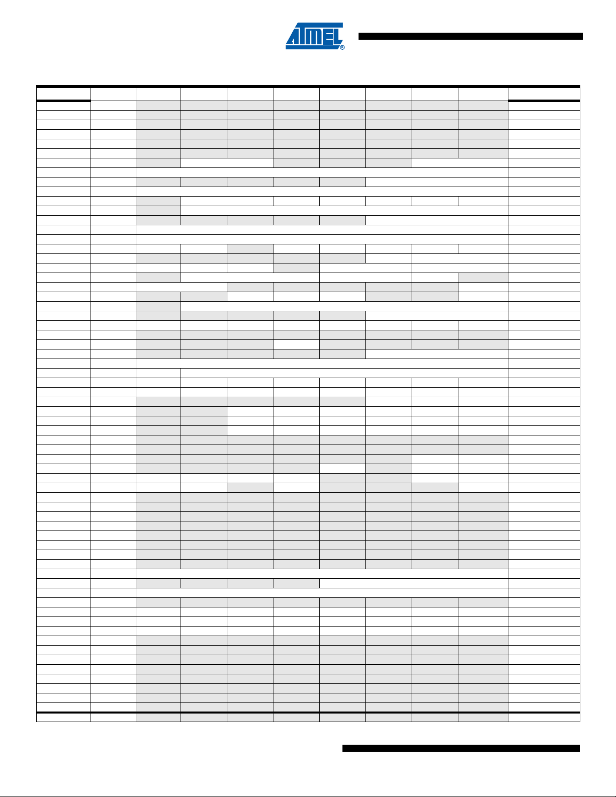
4. Register Summary
Address Name Bit 7 Bit 6 Bit 5 Bit 4 Bit 3 Bit 2 Bit 1 Bit 0 Page
(0xFF) Reserved - - - - - - - (0xFE) Reserved - - - - - - - (0xFD) Reserved - - - - - - - (0xFC) Reserved - - - - - - - (0xFB) Reserved
(0xFA) Reserved
(0xF9) OTGTCON PAGE VALUE
(0xF8) UPINT PINT7:0
(0xF7) UPBCHX - - - - - PBYCT10:8
(0xF6) UPBCLX PBYCT7:0
(0xF5) UPERRX - COUNTER1:0 CRC16 TIMEOUT PID DATAPID DATATGL
(0xF4) UEINT EPINT6:0
(0xF3) UEBCHX - - - - -BYCT10:8
(0xF2) UEBCLX BYCT7:0
(0xF1) UEDATX DAT7:0
(0xF0) UEIENX FLERRE NAKINE - NAKOUTE RXSTPE RXOUTE STALLEDE TXINE
(0xEF) UESTA1X
(0xEE) UESTA0X CFGOK OVERFI UNDERFI
(0xED) UECFG1X EPSIZE2:0 EPBK1:0 ALLOC
(0xEC) UECFG0X EPTYPE1:0 - - EPDIR
(0xEB) UECONX STALLRQ STALLRQC RSTDT EPEN
(0xEA) UERST EPRST6:0
(0xE9) UENUM EPNUM2:0
(0xE8) UEINTX FIFOCON NAKINI RWAL NAKOUTI RXSTPI RXOUTI STALLEDI TXINI
(0xE7) Reserved - - - (0xE6) UDMFN FNCERR
(0xE5) UDFNUMH FNUM10:8
(0xE4) UDFNUML FNUM7:0
(0xE3) UDADDR ADDEN UADD6:0
(0xE2) UDIEN UPRSME EORSME WAKEUPE EORSTE SOFE SUSPE
(0xE1) UDINT UPRSMI EORSMI WAKEUPI EORSTI SOFI SUSPI
(0xE0) UDCON LSM RMWKUP DETACH
(0xDF) OTGINT STOI HNPERRI ROLEEXI BCERRI VBERRI SRPI
(0xDE) OTGIEN STOE HNPERRE ROLEEXE BCERRE VBERRE SRPE
(0xDD) OTGCON HNPREQ SRPREQ SRPSEL VBUSHWC VBUSREQ VBUSRQC
(0xDC) Reserved
(0xDB) Reserved
(0xDA) USBINT IDTI VBUSTI
(0xD9) USBSTA SPEED ID VBUS
(0xD8) USBCON USBE HOST FRZCLK OTGPADE IDTE VBUSTE
(0xD7) UHWCON UIMOD UIDE UVCONE UVREGE
(0xD6) Reserved
(0xD5) Reserved
(0xD4) Reserved
(0xD3) Reserved
(0xD2) Reserved - - - - - - - (0xD1) Reserved
(0xD0) Reserved
(0xCF) Reserved
(0xCE) UDR1 USART1 I/O Data Register
(0xCD) UBRR1H
(0xCC) UBRR1L USART1 Baud Rate Register Low Byte
(0xCB) Reserved
(0xCA) UCSR1C UMSEL11 UMSEL10 UPM11 UPM10 USBS1 UCSZ11 UCSZ10 UCPOL1
(0xC9) UCSR1B RXCIE1 TXCIE1 UDRIE1 RXEN1 TXEN1 UCSZ12 RXB81 TXB81
(0xC8) UCSR1A RXC1 TXC1 UDRE1 FE1 DOR1 PE1 U2X1 MPCM1
(0xC7) Reserved
(0xC6) Reserved
(0xC5) Reserved - - - - - - - (0xC4) Reserved
(0xC3) Reserved - - - - - - - (0xC2) Reserved
(0xC1) Reserved
(0xC0) Reserved - - - - - - - (0xBF) Reserved
- - - - - - - -
- - - - - - - -
- - - - - CTRLDIR CURRBK1:0
- DTSEQ1:0 NBUSYBK1:0
- - - - - - - -
- - - - - - - -
- - - - - - - -
- - - - USART1 Baud Rate Register High Byte
- - - - - - - -
- - - - - - - -
- - - - - - - -
- - - - - - - -
- - - - - - - -
- - - - - - - -
- - - - - - - -
10
7593IS–AVR–02/09
Page 11
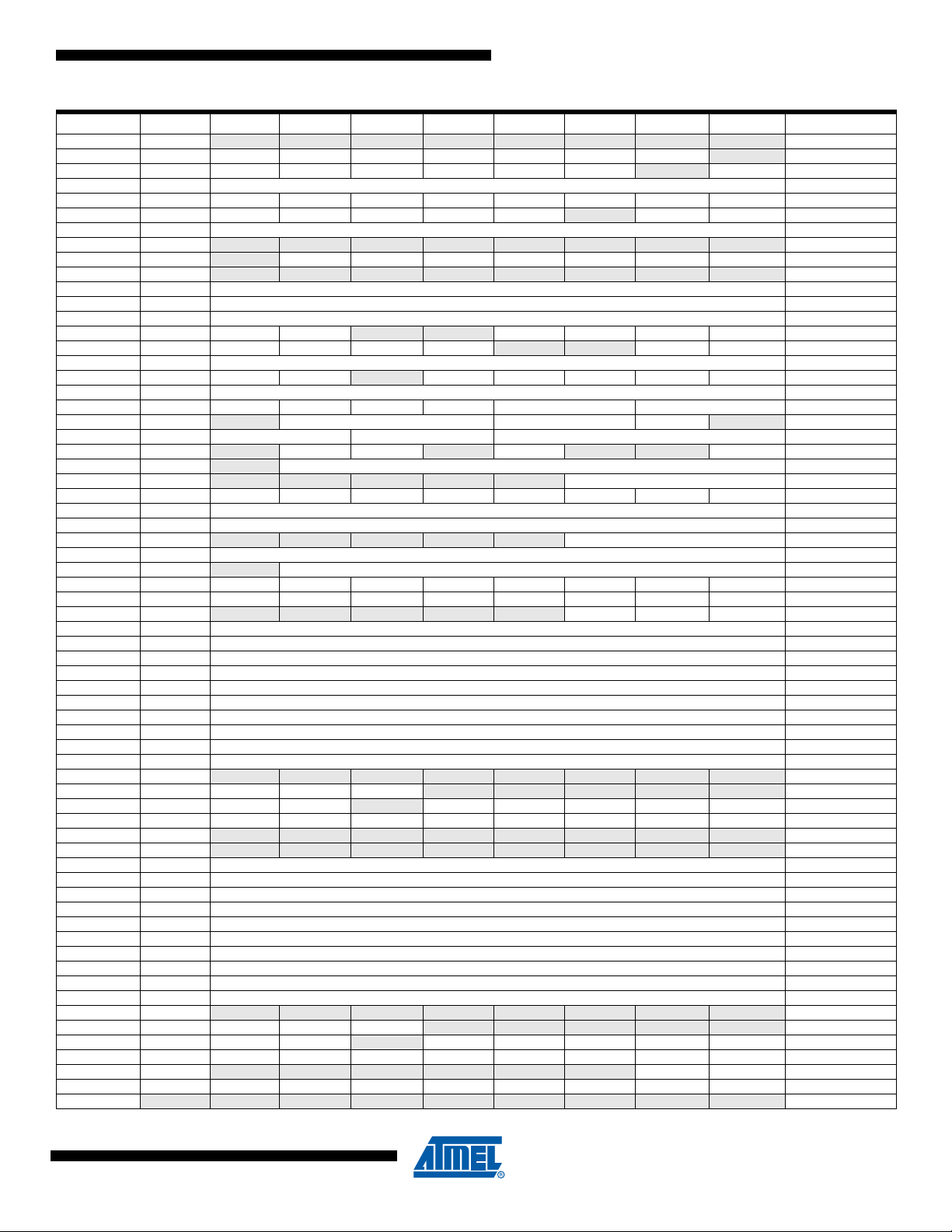
ATmega32U6/AT90USB64/128
Address Name Bit 7 Bit 6 Bit 5 Bit 4 Bit 3 Bit 2 Bit 1 Bit 0 Page
(0xBE) Reserved - - - - - - - (0xBD) TWAMR TWAM6 TWAM5 TWAM4 TWAM3 TWAM2 TWAM1 TWAM0 (0xBC) TWCR TWINT TWEA TWSTA TWSTO TWWC TWEN -TWIE
(0xBB) TWDR 2-wire Serial Interface Data Register
(0xBA) TWAR TWA6 TWA5 TWA4 TWA3 TWA2 TWA1 TWA0 TWGCE
(0xB9) TWSR TWS7 TWS6 TWS5 TWS4 TWS3
(0xB8) TWBR 2-wire Serial Interface Bit Rate Register
(0xB7) Reserved
(0xB6) ASSR - EXCLK AS2 TCN2UB OCR2AUB OCR2BUB TCR2AUB TCR2BUB
(0xB5) Reserved - - - - - - - (0xB4) OCR2B Timer/Counter2 Output Compare Register B
(0xB3) OCR2A Timer/Counter2 Output Compare Register A
(0xB2) TCNT2 Timer/Counter2 (8 Bit)
(0xB1) TCCR2B FOC2A FOC2B - - WGM22 CS22 CS21 CS20
(0xB0) TCCR2A COM2A1 COM2A0 COM2B1 COM2B0 - -WGM21WGM20
(0xAF) UPDATX PDAT7:0
(0xAE) UPIENX FLERRE NAKEDE - PERRE TXSTPE TXOUTE RXSTALLE RXINE
(0xAD) UPCFG2X INTFRQ7:0
(0xAC) UPSTAX CFGOK OVERFI UNDERFI DTSEQ1:0 NBUSYBK1:0
(0xAB) UPCFG1X PSIZE2:0 PBK1:0 ALLOC
(0xAA) UPCFG0X PTYPE1:0 PTOKEN1:0 PEPNUM3:0
(0xA9) UPCONX PFREEZE INMODE RSTDT PEN
(0xA8) UPRST PRST6:0
(0xA7) UPNUM PNUM2:0
(0xA6) UPINTX FIFOCON NAKEDI RWAL PERRI TXSTPI TXOUTI RXSTALLI RXINI
(0xA5) UPINRQX INRQ7:0
(0xA4) UHFLEN FLEN7:0
(0xA3) UHFNUMH FNUM10:8
(0xA2) UHFNUML FNUM7:0
(0xA1) UHADDR HADD6:0
(0xA0) UHIEN HWUPE HSOFE RXRSME RSMEDE RSTE DDISCE DCONNE
(0x9F) UHINT HWUPI HSOFI RXRSMI RSMEDI RSTI DDISCI DCONNI
(0x9E) UHCON RESUME RESET SOFEN
(0x9D) OCR3CH Timer/Counter3 - Output Compare Register C High Byte
(0x9C) OCR3CL Timer/Counter3 - Output Compare Register C Low Byte
(0x9B) OCR3BH Timer/Counter3 - Output Compare Register B High Byte
(0x9A) OCR3BL Timer/Counter3 - Output Compare Register B Low Byte
(0x99) OCR3AH Timer/Counter3 - Output Compare Register A High Byte
(0x98) OCR3AL Timer/Counter3 - Output Compare Register A Low Byte
(0x97) ICR3H Timer/Counter3 - Input Capture Register High Byte
(0x96) ICR3L Timer/Counter3 - Input Capture Register Low Byte
(0x95) TCNT3H Timer/Counter3 - Counter Register High Byte
(0x94) TCNT3L Timer/Counter3 - Counter Regi st e r Lo w By te
(0x93) Reserved - - - - - - - (0x92) TCCR3C FOC3A FOC3B FOC3C
(0x91) TCCR3B ICNC3 ICES3
(0x90) TCCR3A COM3A1 COM3A0 COM3B1 COM3B0 COM3C1 COM3C0 WGM31 WGM30
(0x8F) Reserved
(0x8E) Reserved
(0x8D) OCR1CH Timer/Counter1 - Output Compare Register C High Byte
(0x8C) OCR1CL Timer/Counter1 - Output Compare Register C Low Byte
(0x8B) OCR1BH Timer/Counter1 - Output Compare Register B High Byte
(0x8A) OCR1BL Timer/Counter1 - Output Compare Register B Low Byte
(0x89) OCR1AH Timer/Counter1 - Output Compare Register A High Byte
(0x88) OCR1AL Timer/Counter1 - Output Compare Register A Low Byte
(0x87) ICR1H Timer/Counter1 - Input Capture Register High Byte
(0x86) ICR1L Timer/Counter1 - Input Capture Register Low Byte
(0x85) TCNT1H Timer/Counter1 - Counter Register High Byte
(0x84) TCNT1L Timer/Counter1 - Counter Regi st e r Lo w By te
(0x83) Reserved
(0x82) TCCR1C FOC1A FOC1B FOC1C
(0x81) TCCR1B ICNC1 ICES1 - WGM13 WGM12 CS12 CS11 CS10
(0x80) TCCR1A COM1A1 COM1A0 COM1B1 COM1B0 COM1C1 COM1C0 WGM11 WGM10
(0x7F) DIDR1 - - - - - -AIN1DAIN0D
(0x7E) DIDR0 ADC7D ADC6D ADC5D ADC4D ADC3D ADC2D ADC1D ADC0D
(0x7D)
- - - - - - - - -
- - - - - - - -
- - - - -
- WGM33 WGM32 CS32 CS31 CS30
- - - - - - - -
- - - - - - - -
- - - - - - - -
- - - - -
- TWPS1 TWPS0
7593IS–AVR–02/09
11
Page 12

ATmega32U6/AT90USB64/128
Address Name Bit 7 Bit 6 Bit 5 Bit 4 Bit 3 Bit 2 Bit 1 Bit 0 Page
(0x7C) ADMUX REFS1 REFS0 ADLAR MUX4 MUX3 MUX2 MUX1 MUX0
(0x7B) ADCSRB ADHSM ACME - - - ADTS2 ADTS1 ADTS0
(0x7A) ADCSRA ADEN ADSC ADATE ADIF ADIE ADPS2 ADPS1 ADPS0
(0x79) ADCH ADC Data Register High byte
(0x78) ADCL ADC Data Register Low byte
(0x77) Reserved
(0x76) Reserved
(0x75) XMCRB XMBK - - - - XMM2 XMM1 XMM0
(0x74) XMCRA SRE SRL2 SRL1 SRL0 SRW11 SRW10 SRW01 SRW00
(0x73) Reserved - - - - - - - (0x72) Reserved - - - - - - - (0x71) TIMSK3 - -ICIE3- OCIE3C OCIE3B OCIE3A TOIE3
(0x70) TIMSK2 - - - - - OCIE2B OCIE2A TOIE2
(0x6F) TIMSK1 - -ICIE1- OCIE1C OCIE1B OCIE1A TOIE1
(0x6E) TIMSK0 - - - - - OCIE0B OCIE0A TOIE0
(0x6D) Reserved - - - - - - - (0x6C) Reserved - - - - - - - (0x6B) PCMSK0 PCINT7 PCINT6 PCINT5 PCINT4 PCINT3 PCINT2 PCINT1 PCINT0
(0x6A) EICRB ISC71 ISC70 ISC61 ISC60 ISC51 ISC50 ISC41 ISC40
(0x69) EICRA ISC31 ISC30 ISC21 ISC20 ISC11 ISC10 ISC01 ISC00
(0x68) PCICR - - - - - - -PCIE0
(0x67) Reserved - - - - - - - (0x66) OSCCAL Oscillator Calibration Register
(0x65) PRR1 PRUSB - - -PRTIM3- - PRUSART1
(0x64) PRR0 PRTWI PRTIM2 PRTIM0 -PRTIM1PRSPI - PRADC
(0x63) Reserved - - - - - - - (0x62) Reserved - - - - - - - (0x61) CLKPR CLKPCE - - - CLKPS3 CLKPS2 CLKPS1 CLKPS0
(0x60) WDTCSR WDIF WDIE WDP3 WDCE WDE WDP2 WDP1 WDP0
0x3F (0x5F) SREG I T H S V N Z C
0x3E (0x5E) SPH SP15 SP14 SP13 SP12 SP11 SP10 SP9 SP8
0x3D (0x5D) SPL SP7 SP6 SP5 SP4 SP3 SP2 SP1 SP0
0x3C (0x5C) Reserved - - - - - - - 0x3B (0x5B) RAMPZ - - - - - - RAMPZ1 RAMPZ0
0x3A (0x5A) Reserved - - - - - - - -
0x39 (0x59) Reserved - - - - - - - 0x38 (0x58) Reserved - - - - - - - 0x37 (0x57) SPMCSR SPMIE RWWSB SIGRD RWWSRE BLBSET PGWRT PGERS SPMEN
0x36 (0x56) Reserved - - - - - - - 0x35 (0x55) MCUCR JTD - -PUD- - IVSEL IVCE
0x34 (0x54) MCUSR - - - JTRF WDRF BORF EXTRF PORF
0x33 (0x53) SMCR - - - - SM2 SM1 SM0 SE
0x32 (0x52) Reserved - - - - - - - -
0x31 (0x51)
0x30 (0x50) ACSR ACD ACBG ACO ACI ACIE ACIC ACIS1 ACIS0
0x2F (0x4F) Reserved - - - - - - - 0x2E (0x4E) SPDR SPI Data Register
0x2D (0x4D) SPSR SPIF WCOL - - - - - SPI2X
0x2C (0x4C) SPCR SPIE SPE DORD MSTR CPOL CPHA SPR1 SPR0
0x2B (0x4B) GPIOR2 General Purpose I/O Register 2
0x2A (0x4A) GPIOR1 General Purpose I/O Register 1
0x29 (0x49) PLLCSR
0x28 (0x48) OCR0B Timer/Counter0 Output Compare Register B
0x27 (0x47) OCR0A Timer/Counter0 Output Compare Register A
0x26 (0x46) TCNT0 Timer/Counter0 (8 Bit)
0x25 (0x45) TCCR0B FOC0A FOC0B - - WGM02 CS02 CS01 CS00
0x24 (0x44) TCCR0A COM0A1 COM0A0 COM0B1 COM0B0
0x23 (0x43) GTCCR TSM
0x22 (0x42) EEARH - - - - EEPROM Address Register High Byte
0x21 (0x41) EEARL EEPROM Address Register Low Byte
0x20 (0x40) EEDR EEPROM Data Register
0x1F (0x3F) EECR - - EEPM1 EEPM0 EERIE EEMPE EEPE EERE
0x1E (0x3E) GPIOR0 General Purpose I/O Register 0
0x1D (0x3D) EIMSK INT7 INT6 INT5 INT4 INT3 INT2 INT1 INT0
0x1C (0x3C) EIFR INTF7 INTF6 INTF5 INTF4 INTF3 INTF2 INTF1 INTF0
OCDR/
MONDR
- - - - - - - -
- - - - - - - -
OCDR7 OCDR6 OCDR5 OCDR4 OCDR3 OCDR2 OCDR1 OCDR0
Monitor Data Register
- - - PLLP2 PLLP1 PLLP0 PLLE PLOCK
- -WGM01WGM00
- - - - - PSRASY PSRSYNC
12
7593IS–AVR–02/09
Page 13

ATmega32U6/AT90USB64/128
Address Name Bit 7 Bit 6 Bit 5 Bit 4 Bit 3 Bit 2 Bit 1 Bit 0 Page
0x1B (0x3B) PCIFR - - - - - - -PCIF0
0x1A (0x3A) Reserved - - - - - - - -
0x19 (0x39) Reserved - - - - - - - -
0x18 (0x38) TIFR3 - -ICF3- OCF3C OCF3B OCF3A TOV3
0x17 (0x37) TIFR2 - - - - - OCF2B OCF2A TOV2
0x16 (0x36) TIFR1
0x15 (0x35) TIFR0
0x14 (0x34) Reserved - - - - - - - -
0x13 (0x33) Reserved - - - - - - - -
0x12 (0x32) Reserved - - - - - - - -
0x11 (0x31) PORTF PORTF7 PORTF6 PORTF5 PORTF4 PORTF3 PORTF2 PORTF1 PORTF0
0x10 (0x30) DDRF DDF7 DDF6 DDF5 DDF4 DDF3 DDF2 DDF1 DDF0
0x0F (0x2F) PINF PINF7 PINF6 PINF5 PINF4 PINF3 PINF2 PINF1 PINF0
0x0E (0x2E) PORTE PORTE7 PORTE6 PORTE5 PORTE4 PORTE3 PORTE2 PORTE1 PORTE0
0x0D (0x2D) DDRE DDE7 DDE6 DDE5 DDE4 DDE3 DDE2 DDE1 DDE0
0x0C (0x2C) PINE PINE7 PINE6 PINE5 PINE4 PINE3 PINE2 PINE1 PINE0
0x0B (0x2B) PORTD PORTD7 PORTD6 PORTD5 PORTD4 PORTD3 PORTD2 PORTD1 PORTD0
0x0A (0x2A) DDRD DDD7 DDD6 DDD5 DDD4 DDD3 DDD2 DDD1 DDD0
0x09 (0x29) PIND PIND7 PIND6 PIND5 PIND4 PIND3 PIND2 PIND1 PIND0
0x08 (0x28) PORTC PORTC7 PORTC6 PORTC5 PORTC4 PORTC3 PORTC2 PORTC1 PORTC0
0x07 (0x27) DDRC DDC7 DDC6 DDC5 DDC4 DDC3 DDC2 DDC1 DDC0
0x06 (0x26) PINC PINC7 PINC6 PINC5 PINC4 PINC3 PINC2 PINC1 PINC0
0x05 (0x25) PORTB PORTB7 PORTB6 PORTB5 PORTB4 PORTB3 PORTB2 PORTB1 PORTB0
0x04 (0x24) DDRB DDB7 DDB6 DDB5 DDB4 DDB3 DDB2 DDB1 DDB0
0x03 (0x23) PINB PINB7 PINB6 PINB5 PINB4 PINB3 PINB2 PINB1 PINB0
0x02 (0x22) PORTA PORTA7 PORTA6 PORTA5 PORTA4 PORTA3 PORTA2 PORTA1 PORTA0
0x01 (0x21) DDRA DDA7 DDA6 DDA5 DDA4 DDA3 DDA2 DDA1 DDA0
0x00 (0x20) PINA PINA7 PINA6 PINA5 PINA4 PINA3 PINA2 PINA1 PINA0
Note: 1. For compatibility with future devices, reserved bits should be written to zero if accessed. Reserved I/O memory addresses
should never be written.
2. I/O registers within the address range $00 - $1F are directly bit-accessible using the SBI and CBI instructions. In these registers, the value of single bits can be checked by using the SBIS and SBIC instructions.
3. Some of the status flags are cleared by writing a logical one to them. Note that the CBI and SBI instructions will o perate on
all bits in the I/O register, writing a one back into any flag read as set, thus clearing the flag. The CBI and SBI instruction s
work with registers 0x00 to 0x1F on ly.
4. When using the I/O specific commands IN and OUT, the I/O addresses $00 - $3F must be used. When addressing I/O registers as data space using LD and ST instructions, $20 must be added to these addresses. The
ATmega32U6/AT90USB64/128 is a complex microcontroller with more peripheral units than can be supported within the 64
location reserved in Opcode for the IN and OUT instructions. For the Extended I/O space from $60 - $1FF in SRAM, only the
ST/STS/STD and LD/LDS/LDD instructions can be used.
- -ICF1- OCF1C OCF1B OCF1A TOV1
- - - - - OCF0B OCF0A TOV0
7593IS–AVR–02/09
13
Page 14

ATmega32U6/AT90USB64/128
5. Instruction Set Summary
Mnemonics Operands Description Operation Flags #Clocks
ADD Rd, Rr Add two Registers Rd ← Rd + Rr Z,C,N,V,H 1
ADC Rd, Rr Add with Carry two Registers Rd ← Rd + Rr + C Z,C,N,V,H 1
ADIW Rdl,K Add Immediate to Word Rdh:Rdl ← Rdh:Rdl + K Z,C,N,V,S 2
SUB Rd, Rr Subtract two Registers Rd ← Rd - Rr Z,C,N,V,H 1
SUBI Rd, K Subtract Constant from Register Rd ← Rd - K Z,C,N,V,H 1
SBC Rd, Rr Subtract with Carry two Registers Rd ← Rd - Rr - C Z,C,N,V,H 1
SBCI Rd, K Subtract with Carry Constant from Reg. Rd ← Rd - K - C Z,C,N,V,H 1
SBIW Rdl,K Subtract Immediate from Word Rdh:Rdl ← Rdh:Rdl - K Z,C,N,V,S 2
AND Rd, Rr Logical AND Registers Rd ← Rd • Rr Z,N,V 1
ANDI Rd, K Logical AND Register and Constant Rd ← Rd • K Z,N,V 1
OR Rd, Rr Logical OR Registers Rd ← Rd v Rr Z,N,V 1
ORI Rd, K Logical OR Register and Constant Rd ← Rd v K Z,N,V 1
EOR Rd, Rr Exclusive OR Registers Rd ← Rd ⊕ Rr Z,N,V 1
COM Rd One’s Complement Rd ← 0xFF − Rd Z,C,N,V 1
NEG Rd Two’s Complement Rd ← 0x00 − Rd Z,C,N,V,H 1
SBR Rd,K Set Bit(s) in Register Rd ← Rd v K Z,N,V 1
CBR Rd,K Clear Bit(s) in Register Rd ← Rd • (0xFF - K) Z,N,V 1
INC Rd Increment Rd ← Rd + 1 Z,N,V 1
DEC Rd Decrement Rd ← Rd − 1 Z,N,V 1
TST Rd Test for Zero or Minus Rd ← Rd • Rd Z,N,V 1
CLR Rd Clear Register Rd ← Rd ⊕ Rd Z,N,V 1
SER Rd Set Register Rd ← 0xFF None 1
MUL Rd, Rr Multiply Unsigned R1:R0 ← Rd x Rr Z,C 2
MULS Rd, Rr Multiply Signed R1:R0 ← Rd x Rr Z,C 2
MULSU Rd, Rr Multiply Signed with Unsigned R1:R0 ← Rd x Rr Z,C 2
FMUL Rd, Rr Fractional Multiply Unsigned R1:R0 ← (Rd x Rr) << 1 Z,C 2
FMULS Rd, Rr Fractional Multiply Signed R1:R0 ← (Rd x Rr) << 1 Z,C 2
FMULSU Rd, Rr Fractional Multiply Signed with Unsigned R1:R0 ← (Rd x Rr) << 1 Z,C 2
RJMP k Relative Jump PC ← PC + k + 1 None 2
IJMP Indirect Jump to (Z) PC ← Z None 2
EIJMP Extended Indirect Jump to (Z)
JMP k Direct Jump PC ← kNone3
RCALL k Relative Subroutine Call PC ← PC + k + 1 None 4
ICALL Indirect Call to (Z) PC ← ZNone4
EICALL Extended Indirect Call to (Z)
CALL k Direct Subroutine Call PC ← kNone5
RET Subroutine Return PC ← STACK None 5
RETI Interrupt Return PC ← STACK I 5
CPSE Rd,Rr Compare, Skip if Equal if (Rd = Rr) PC ← PC + 2 or 3 None 1/2/3
CP Rd,Rr Compare Rd − Rr Z, N,V,C,H 1
CPC Rd,Rr Compare with Carry Rd − Rr − C Z, N,V,C,H 1
CPI Rd,K Compare Register with Immediate Rd − K Z, N,V,C,H 1
SBRC Rr, b Skip if Bit in Register Cleared if (Rr(b)=0) PC ← PC + 2 or 3 None 1/2/3
SBRS Rr, b Skip if Bit in Register is Set if (Rr(b)=1) PC ← PC + 2 or 3 None 1/2/3
SBIC P, b Skip if Bit in I/O Register Cleared if (P(b)=0) PC ← PC + 2 or 3 None 1/2/3
SBIS P, b Skip if Bit in I/O Register is Set if (P(b)=1) PC ← PC + 2 or 3 None 1/2/3
BRBS s, k Branch if Status Flag Set if (SREG(s) = 1) then PC←PC+k + 1 None 1/2
BRBC s, k Branch if Status Flag Cleared if (SREG(s) = 0) then PC←PC+k + 1 None 1/2
BREQ k Branch if Equal if (Z = 1) then PC ← PC + k + 1 None 1/2
BRNE k Branch if Not Equal if (Z = 0) then PC ← PC + k + 1 None 1/2
BRCS k Branch if Carry Set if (C = 1) then PC ← PC + k + 1 None 1/2
BRCC k B ranch if Carry Cleared if (C = 0) then PC ← PC + k + 1 None 1/2
BRSH k Branch if Same or Higher if (C = 0) then PC ← PC + k + 1 None 1/2
BRLO k Branch if Lower if (C = 1) then PC ← PC + k + 1 None 1/2
BRMI k Branch if Minus if (N = 1) then PC ← PC + k + 1 None 1/2
BRPL k Branch if Plus if (N = 0) then PC ← PC + k + 1 None 1/2
BRGE k Branch if Greater or Equal, Signed if (N ⊕ V= 0) then PC ← PC + k + 1 None 1/2
BRLT k Branch if Less Than Zero, Signed if (N ⊕ V= 1) then PC
BRHS k Branch if Half Carry Flag Set if (H = 1) then PC ← PC + k + 1 None 1/2
BRHC k Branch if Half Carry Flag Cleared if (H = 0) then PC ← PC + k + 1 None 1/2
BRTS k Branch if T Flag Set if (T = 1) then PC ← PC + k + 1 None 1/2
BRTC k Branch if T Flag Cleared if (T = 0) then PC ← PC + k + 1 None 1/2
BRVS k Branch if Overflow Flag is Set if (V = 1) then PC ← PC + k + 1 None 1/2
ARITHMETIC AND LOGIC INSTRUCTIONS
BRANCH INSTRUCTIONS
PC ←(EIND:Z)
PC ←(EIND:Z)
← PC + k + 1 None 1/2
None 2
None 4
14
7593IS–AVR–02/09
Page 15
ATmega32U6/AT90USB64/128
Mnemonics Operands Description Operation Flags #Clocks
BRVC k Branch if Overflow Flag is Cleared if (V = 0) then PC ← PC + k + 1 None 1/2
BRIE k Branch if Interrupt Enabled if ( I = 1) then PC ← PC + k + 1 None 1/2
BRID k Branch if Interrupt Disabled if ( I = 0) then PC ← PC + k + 1 None 1/2
SBI P,b Set Bit in I/O Register I/O(P,b) ← 1None2
CBI P,b Clear Bit in I/O Register I/O(P,b) ← 0None2
LSL Rd Logical Shift Left Rd(n+1) ← Rd(n), Rd(0) ← 0 Z,C,N,V 1
LSR Rd Logical Shift Right Rd(n) ← Rd(n+1), Rd(7) ← 0 Z,C,N,V 1
ROL Rd Rotate Left Through Carry Rd(0)←C,Rd(n+1)← Rd(n),C← Rd(7) Z,C,N,V 1
ROR Rd Rotate Right Through Carry Rd(7)←C,Rd(n)← Rd(n+1),C←Rd(0) Z,C,N,V 1
ASR Rd Arithmetic Shift Right Rd(n) ← Rd(n+1), n=0..6 Z,C,N,V 1
SWAP Rd Swap Nibbles Rd(3..0)←Rd(7..4),Rd(7..4)←Rd(3..0) None 1
BSET s Flag Set SREG(s) ← 1 SREG(s) 1
BCLR s Flag Clear SREG(s) ← 0 SREG(s) 1
BST Rr, b Bit Store from Register to T T ← Rr(b) T 1
BLD Rd, b Bit load from T to Register Rd(b) ← TNone1
SEC Set Carry C ← 1C1
CLC Clear Carry C ← 0 C 1
SEN Set Negative Flag N ← 1N1
CLN Clear Negative Flag N ← 0 N 1
SEZ Set Zero Flag Z ← 1Z1
CLZ Clear Zero Flag Z ← 0 Z 1
SEI Global Interrupt Enable I ← 1I1
CLI Global Interrupt Disable I ← 0 I 1
SES Set Signed Test Flag S ← 1S1
CLS Clear Signed Test Flag S ← 0 S 1
SEV Set Twos Complement Overflow. V ← 1V1
CLV Clear Twos Complement Overflow V ← 0 V 1
SET Set T in SREG T ← 1T1
CLT Clear T in SREG T ← 0 T 1
SEH Set Half Carry Flag in SREG H ← 1H1
CLH Clear Half Carry Flag in SREG H ← 0 H 1
MOV Rd, Rr Move Between Registers Rd ← Rr None 1
MOVW Rd, Rr Copy Register Word
LDI Rd, K Load Immediate Rd ← KNone1
LD Rd, X Load Indirect Rd ← (X) None 2
LD Rd, X+ Load Indirect and Post-Inc. Rd ← (X), X ← X + 1 None 2
LD Rd, - X Load Indirect and Pre-Dec. X ← X - 1, Rd ← (X) None 2
LD Rd, Y Load Indirect Rd ← (Y) None 2
LD Rd, Y+ Load Indirect and Post-Inc. Rd ← (Y), Y ← Y + 1 None 2
LD Rd, - Y Load Indirect and Pre-Dec. Y ← Y - 1, Rd ← (Y) None 2
LDD Rd,Y+q Load Indirect with Displacement Rd ← (Y + q) None 2
LD Rd, Z Load Indirect Rd ← (Z) None 2
LD Rd, Z+ Load Indirect and Post-Inc. Rd ← (Z), Z ← Z+1 None 2
LD Rd, -Z Load Indirect and Pre-Dec. Z ← Z - 1, Rd ← (Z) None 2
LDD Rd, Z+q Load Indirect with Displacement Rd ← (Z + q) None 2
LDS Rd, k Load Direct from SRAM Rd ← (k) None 2
ST X, Rr Store Indirect (X) ← Rr None 2
ST X+, Rr Store Indirect and Post-Inc. (X) ← Rr, X ← X + 1 None 2
ST - X, Rr Store Indirect and Pre-Dec. X ← X - 1, (X) ← Rr None 2
ST Y, Rr Store Indirect (Y) ← Rr None 2
ST Y+, Rr Store Indirect and Post-Inc. (Y) ← Rr, Y ← Y + 1 None 2
ST - Y, Rr Store Indirect and Pre-Dec. Y ← Y - 1, (Y) ← Rr None 2
STD Y+q,Rr Store Indirect with Displacement (Y + q) ← Rr None 2
ST Z, Rr Store Indirect (Z) ← Rr None 2
ST Z+, Rr Store Indirect and Post-Inc. (Z) ← Rr, Z ← Z + 1 None 2
ST -Z, Rr Store Indirect and Pre-Dec. Z ← Z - 1, (Z) ← Rr None 2
STD Z+q,Rr Store Indirect with Displacement (Z + q) ← Rr None 2
STS k, Rr Store Direct to SRAM (k) ← Rr None 2
LPM Load Program Memory R0 ← (Z) None 3
LPM Rd, Z Load Program Memory Rd ← (Z) None 3
LPM Rd, Z+ Load Program Memory and Post-Inc Rd ← (Z), Z ← Z+1 None 3
ELPM Extended Load Program Memory R0 ← (RAMPZ:Z) None 3
ELPM Rd, Z Extended Load Program Memory Rd ← (Z) None 3
ELPM Rd, Z+ Extended Load Program Memory Rd ← (RAMPZ:Z), RAMPZ:Z ←RAMPZ:Z+1 None 3
BIT AND BIT-TEST INSTRUCTIONS
DATA TRANSFER INSTRUCTIONS
Rd+1:Rd ← Rr+1:Rr
None 1
7593IS–AVR–02/09
15
Page 16

ATmega32U6/AT90USB64/128
Mnemonics Operands Description Operation Flags #Clocks
SPM Store Program Memory (Z) ← R1:R0 None -
IN Rd, P In Port Rd ← PNone1
OUT P, Rr Out Port P ← Rr Non e 1
PUSH Rr Push Register on Stack STACK ← Rr None 2
POP Rd Pop Register from Stack Rd ← STACK None 2
NOP No Operation None 1
SLEEP Sleep (see spec ific descr. for Sleep function) None 1
WDR Watchdog Reset (see specific descr. for WDR/timer) None 1
BREAK Break For On-chip Debug Only None N/A
MCU CONTROL INSTRUCTIONS
16
7593IS–AVR–02/09
Page 17
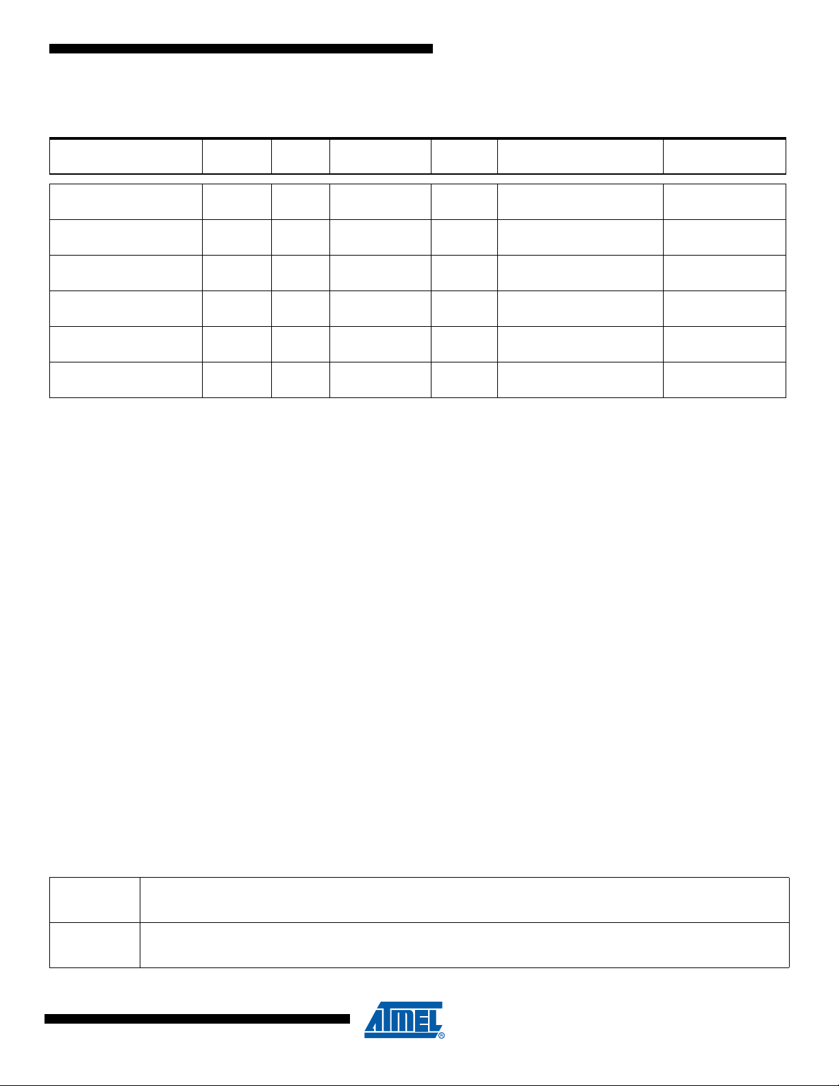
6. Ordering Information
Table 6-1. Possible Order Entries
USB
Ordering Code
interface
Speed
(MHz)
ATmega32U6/AT90USB64/128
Power Supply
(V) Package Operation Range Product Marking
AT90USB1287-16AU OTG 8-16 2.7 - 5.5 MD
AT90USB1287-16MU
AT
90USB1286-16MU
AT90USB647-16AU OTG 8-16 2.7 - 5.5 MD
AT90USB647-16MU
AT
90USB646-16MU
OTG 8-16 2.7 - 5.5 PS
Device
only
OTG 8-16 2.7 - 5.5 PS
Device
only
8-16 2.7 - 5.5 PS
8-16 2.7 - 5.5 PS
Industrial (-40° to +85°C)
Green
Industrial (-40° to +85°C)
Green
Industrial (-40° to +85°C)
Green
Industrial (-40° to +85°C)
Green
Industrial (-40° to +85°C)
Green
Industrial (-40° to +85°C)
Green
90USB1287-16AU
90USB1287-16MU
90USB1286-16MU
90USB647-16AU
90USB647-16MU
90USB646-16MU
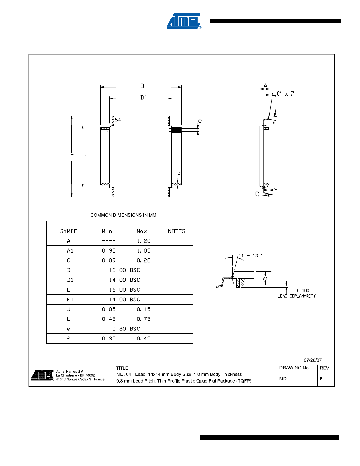
MD 64 - Lead, 14x14 mm Body Size, 1.0mm Body Thickness
0.8 mm Lead Pitch, Thin Profile Plastic Quad Flat Package (TQFP)
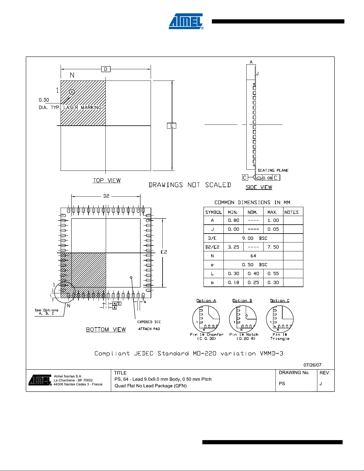
PS 64 - Lead, 9x9 mm Body Size, 0.50mm Pitch
Quad Flat No Lead Package (QFN)
7593IS–AVR–02/09
17
Page 18
ATmega32U6/AT90USB64/128
6.1 TQFP64
18
7593IS–AVR–02/09
Page 19

ATmega32U6/AT90USB64/128
7593IS–AVR–02/09
19
Page 20
ATmega32U6/AT90USB64/128
6.2 QFN64
20
7593IS–AVR–02/09
Page 21
ATmega32U6/AT90USB64/128
7593IS–AVR–02/09
21
Page 22

ATmega32U6/AT90USB64/128
7. Errata
8. AT90USB1287/6 Errata.
8.1 AT90USB1287/6 Errata History
Silicon
Release
First Release Date Code up to 0648
Second Release
Third Release
90USB1286-16MU 90USB1287-16AU 90USB1287-16MU
Date Code from 0709 to 0801
except lots 0801 7H5103*
Lots 0801 7H5103* and
Date Code from 0814
Note ‘*’ means a blank or any alphanumeric string
8.2 AT90USB1287/6 First Release
• Incorrect CPU behavior for VBUSTI and IDTI inter rupts rout ines
• USB Eye Diagram violation in low-speed mode
• Transient perturbation in USB suspend mode generates over consumption
• VBUS Session valid threshold voltage
• USB signal rate
• VBUS residual level
• Spike on TWI pins when TWI is enabled
• High current consumption in sleep mode
• Async timer interrupt wake up from sleep generate multiple interrupts
Date Code up to 0714
and lots 0735 6H2726*
from Date Code 0722 to 0806
except lots 0735 6H2726*
Date Code from 0814
Date Code up to 0701
Date Code from 0714 to 0810
except lots 0748 7H5103*
Lots 0748 7H5103* and
Date Code from 0814
22
9. Incorrect CPU behavior for VBUSTI and IDTI interrupts routines
The CPU core may incorrectly execute the interrupt vector related to the VBUSTI and IDTI
interrupt flags.
Problem fix/workaround
Do not enable these interrupts, firmware must process these USB events by polling VBUSTI
and IDTI flags.
8. USB Eye Diagram violation in low-speed mode
The low to high transition of D- violates t he USB eye di agram specificati on when tr ansmitting
with low-speed signaling.
Problem fix/workaround
None.
7. Transient perturbation in USB suspend mode generates overconsumption
In device mode and when the USB is suspended, transient perturbation received on the
USB lines generates a wake up state. However the idle state f ollowing the per turbation does
7593IS–AVR–02/09
Page 23

ATmega32U6/AT90USB64/128
not set the SUSPI bit anymore. The internal USB engine remains in suspend mode but the
USB differential receiver is still enabled and generates a typical 300µA extra-power consumption. Detection of the suspend state after the transient perturbation should be
performed by software (instead of reading the SUSPI bit).
Problem fix/workaround
USB waiver allows bus powered devices to consume up to 2.5mA in suspend state.
6. VBUS Session valid threshold voltage
The VSession valid threshold voltage is internally connected to VBus_Valid (4.4V approx.).
That causes the device to attach to the bus only when Vbus is greater than VBusValid
instead of V_Session Valid. Thus if VBUS is lower than 4.4V, the device is detached.
Problem fix/workaround
According to the USB power drop budget, this may require connecting the device toa root
hub or a self-powered hub.
5. UBS signal rate
The average USB signal rate may sometime be measured out of the USB specificatio ns
(12MHz ±30kHz) with short frames. When measured on a long period, the average signal
rate value complies with the specifications. This bit rate deviation does not generates communication or functional errors.
Problem fix/workaround
None.
4. VBUS residual level
In USB device and host mode, once a 5V level has been detected to the VBUS pad, a residual level (about 3V) can be measured on the VBUS pin.
Problem fix/workaround
None.
3. Spike on TWI pins when TWI is enabled
100 ns negative spike occurs on SDA and SCL pins when TWI is enabled.
Problem Fix/workaround
No known workaround, enable ATmega32U6/AT90USB64/128 TWI first versus the others
nodes of the TWI network.
2. High current consumption in sleep mode
If a pending interrupt cannot wake the part up from the selected mod e, the current consumption will increase during sleep when executing the SLEEP instruction directly after a SEI
instruction.
Problem Fix/workaround
Before entering sleep, interrupts not used to wake up the part from the sleep mode should
be disabled.
7593IS–AVR–02/09
1. Asynchronous timer interrupt wake up from sleep generates multiple interrupts
23
Page 24

ATmega32U6/AT90USB64/128
If the CPU core is in sleep and wakes-up from an asynchronous timer interrupt and then go
back in sleep again it may wake up multiple times.
Problem Fix/workaround
A software workaround is to wait with performing the sleep instruction until
TCNT2>OCR2+1.
24
7593IS–AVR–02/09
Page 25

8.3 AT90USB1287/6 Second Release
• Incorrect CPU behavior for VBUSTI and IDTI inter rupts rout ines
• USB Eye Diagram violation in low-speed mode
• Transient perturbation in USB suspend mode generates over consumption
• VBUS Session valid threshold voltage
• Spike on TWI pins when TWI is enabled
• High current consumption in sleep mode
• Async timer interrupt wake up from sleep generate multiple interrupts
7. Incorrect CPU behavior for VBUSTI and IDTI interrupts routines
The CPU core may incorrectly execute the interrupt vector related to the VBUSTI and IDTI
interrupt flags.
Problem fix/workaround
Do not enable these interrupts, firmware must process these USB events by polling VBUSTI
and IDTI flags.
6. USB Eye Diagram violation in low-speed mode
ATmega32U6/AT90USB64/128
The low to high transition of D- violates t he USB eye di agram specificati on when tr ansmitting
with low-speed signaling.
Problem fix/workaround
None.
5. Transient perturbation in USB suspend mode generates overconsumption
In device mode and when the USB is suspended, transient perturbation received on the
USB lines generates a wake up state. However the idle state f ollowing the per turbation does
not set the SUSPI bit anymore. The internal USB engine remains in suspend mode but the
USB differential receiver is still enabled and generates a typical 300µA extra-power consumption. Detection of the suspend state after the transient perturbation should be
performed by software (instead of reading the SUSPI bit).
Problem fix/workaround
USB waiver allows bus powered devices to consume up to 2.5mA in suspend state.
4. VBUS Session valid threshold voltage
The VSession valid threshold voltage is internally connected to VBus_Valid (4.4V approx.).
That causes the device to attach to the bus only when Vbus is greater than VBusValid
instead of V_Session Valid. Thus if VBUS is lower than 4.4V, the device is detached.
Problem fix/workaround
According to the USB power drop budget, this may require connecting the device toa root
hub or a self-powered hub.
7593IS–AVR–02/09
3. Spike on TWI pins when TWI is enabled
100 ns negative spike occurs on SDA and SCL pins when TWI is enabled.
25
Page 26

ATmega32U6/AT90USB64/128
Problem Fix/workaround
No known workaround, enable ATmega32U6/AT90USB64/128 TWI first versus the others
nodes of the TWI network.
2. High current consumption in sleep mode
If a pending interrupt cannot wake the part up from the selected mod e, the current consumption will increase during sleep when executing the SLEEP instruction directly after a SEI
instruction.
Problem Fix/workaround
Before entering sleep, interrupts not used to wake up the part from the sleep mode should
be disabled.
1. Asynchronous timer interrupt wake up from sleep generates multiple interrupts
If the CPU core is in sleep and wakes-up from an asynchronous timer interrupt and then go
back in sleep again it may wake up multiple times.
Problem Fix/workaround
A software workaround is to wait with performing the sleep instruction until
TCNT2>OCR2+1.
26
7593IS–AVR–02/09
Page 27

8.4 AT90USB1287/6 Third Release
• Incorrect CPU behavior for VBUSTI and IDTI inter rupts rout ines
• Transient perturbation in USB suspend mode generates over consumption
• Spike on TWI pins when TWI is enabled
• High current consumption in sleep mode
• Async timer interrupt wake up from sleep generate multiple interrupts
5. Incorrect CPU behavior for VBUSTI and IDTI interrupts routines
The CPU core may incorrectly execute the interrupt vector related to the VBUSTI and IDTI
interrupt flags.
Problem fix/workaround
Do not enable these interrupts, firmware must process these USB events by polling VBUSTI
and IDTI flags.
4. Transient perturbation in USB suspend mode generates overconsumption
In device mode and when the USB is suspended, transient perturbation received on the
USB lines generates a wake up state. However the idle state f ollowing the per turbation does
not set the SUSPI bit. The internal USB e ngine remains in suspend mode but the USB differential receiver is still enabled and generates a typical 300µA extra-power consumption.
Detection of the suspend state after the transient perturbation should be performed by software (instead of reading the SUSPI bit).
ATmega32U6/AT90USB64/128
Problem fix/workaround
USB waiver allows bus powered devices to consume up to 2.5mA in suspend state.
3. Spike on TWI pins when TWI is enabled
100 ns negative spike occurs on SDA and SCL pins when TWI is enabled.
Problem Fix/workaround
No known workaround, enable ATmega3 2U6/AT90USB64/128 TW I first, before the others
nodes of the TWI network.
2. High current consumption in sleep mode
If a pending interrupt cannot wake the part up from the selected mod e, the current consumption will increase during sleep when executing the SLEEP instruction directly after a SEI
instruction.
Problem Fix/workaround
Before entering sleep, interrupts not used to wake up the part from sleep mode should be
disabled.
1. Asynchronous timer interrupt wake up from sleep generates multiple interrupts
If the CPU core is in sleep mode and wakes-up from an asynchronous timer interrupt and
then goes back into sleep mode, it may wake up multiple times.
7593IS–AVR–02/09
Problem Fix/workaround
27
Page 28

ATmega32U6/AT90USB64/128
A software workaround is to wait beforeperforming the slee p instruction: until
TCNT2>OCR2+1.
9. AT90USB647/6 Errata.
• Incorrect interrupt routine exection for VBUSTI, IDTI interrupts flags
• USB Eye Diagram violation in low-speed mode
• Transient perturbation in USB suspend mode generates over consumption
• Spike on TWI pins when TWI is enabled
• High current consumption in sleep mode
• Async timer interrupt wake up from sleep generate multiple interrupts
6. Incorrect CPU behavior for VBUSTI and IDTI interrupts routines
The CPU core may incorrectly execute the interrupt vector related to the VBUSTI and IDTI
interrupt flags.
Problem fix/workaround
Do not enable these interrupts, firmware must process these USB events by polling VBUSTI
and IDTI flags.
5. USB Eye Diagram violation in low-speed mode
The low to high transition of D- violates t he USB eye di agram specificati on when tr ansmitting
with low-speed signaling.
Problem fix/workaround
None.
4. Transient perturbation in USB suspend mode generates overconsumption
In device mode and when the USB is suspended, transient perturbation received on the
USB lines generates a wake up state. However the idle state f ollowing the per turbation does
not set the SUSPI bit anymore. The internal USB engine remains in suspend mode but the
USB differential receiver is still enabled and generates a typical 300µA extra-power consumption. Detection of the suspend state after the transient perturbation should be
performed by software (instead of reading the SUSPI bit).
Problem fix/workaround
USB waiver allows bus powered devices to consume up to 2.5mA in suspend state.
3. Spike on TWI pins when TWI is enabled
100 ns negative spike occurs on SDA and SCL pins when TWI is enabled.
Problem Fix/workaround
No known workaround, enable ATmega32U6/AT90USB64/128 TWI first versus the others
nodes of the TWI network.
2. High current consumption in sleep mode
28
7593IS–AVR–02/09
Page 29

If a pending interrupt cannot wake the part up from the selected mod e, the current consumption will increase during sleep when executing the SLEEP instruction directly after a SEI
instruction.
Problem Fix/workaround
Before entering sleep, interrupts not used to wake up the part from the sleep mode should
be disabled.
1. Asynchronous timer interrupt wake up from sleep generates multiple interrupts
If the CPU core is in sleep and wakes-up from an asynchronous timer interrupt and then go
back in sleep mode again it may wake up several times.
Problem Fix/workaround
A software workaround is to wait with performing the sleep instruction until
TCNT2>OCR2+1.
10. ATmega32U6 Errata.
• Spike on TWI pins when TWI is enabled
• Async timer interrupt wake up from sleep generate multiple interrupts
ATmega32U6/AT90USB64/128
2. Spike on TWI pins when TWI is enabled
100 ns negative spike occurs on SDA and SCL pins when TWI is enabled.
Problem Fix/workaround
No known workaround, enable ATmega32U6/AT90USB64/128 TWI first versus the others
nodes of the TWI network.
1. Asynchronous timer interrupt wake up from sleep generates multiple interrupts
If the CPU core is in sleep and wakes-up from an asynchronous timer interrupt and then go
back in sleep mode again it may wake up several times.
Problem Fix/workaround
A software workaround is to wait with performing the sleep instruction until
TCNT2>OCR2+1.
7593IS–AVR–02/09
29
Page 30

ATmega32U6/AT90USB64/128
11. Datasheet Revision History for ATmega32U6/AT90USB64/128
Please note that the referring page numbers in this section are referred to this document. The
referring revision in this section are referring to the document revision.
11.1 Changes from 7593A to 7593B
1. Changed default configuration for fuse byte s and security byte.
2. Suppression of timer 4,5 registers which does not exist.
3. Updated typical application schematics in USB section
11.2 Changes from 7593B to 7593C
1. Update to package drawings, MQFP64 and TQFP64.
11.3 Changes from 7593C to 7593D
1. For further product compatibility, changed USB PLL possible prescaler configurations.
Only 8MHz and 16MHz crystal frequencies allows USB operation (See Table 6-11 on
page 49).
11.4 Changes from 7593D to 7593E
1. Updated PLL Prescaler table: configuration words are different between AT90USB64x
and AT90USB128x to enable the PLL with a 16 MHz source.
2. Cleaned up some bits from USB registers, and updat ed information about OTG timers ,
remote wake-up, reset and connection timings.
3. Updated clock distribution tree diagram (USB prescaler source and configuration
register).
4. Cleaned up register summary.
5. Suppressed PCINT23:8 that do not exist from External Interrupts.
6. Updated Electrical Characteristics.
7. Added Typical Characteristics.
8. Update Errata section.
11.5 Changes from 7593E to 7593F
1. Removed ’Preliminary’ from document status.
2. Clarification in Stand by mode regarding USB.
11.6 Changes from 7593F to 7593G
1. Updated Errata section.
11.7 Changes from 7593G to 7593H
1. Added Signature information for 64K devices.
2. Fixed figure for typical bus powered application
3. Added min/max values for BOD levels
4. Added ATmega32U6 product
5. Update Errata section
6. Modified descriptions for HWUPE and WAKEUPE interrupts enable (these interrupts
should be enabled only to wake up the CPU core from power down mode).
30
7593IS–AVR–02/09
Page 31

7. Added description to access unique serial number located in Signature Row see
“Reading the Signature Row from Software” on page 360.
11.8 Changes from 7593H to 7593I
1. Updated Table 8-2 in “Brown-out Detection” on page 60. Unused BOD levels removed.
ATmega32U6/AT90USB64/128
7593IS–AVR–02/09
31
 Loading...