


BDTIC www.bdtic.com/ATMEL
Features
• High Perf ormance, Low Power AVR
• Advanced RISC Architecture
– 125 Powerful Instructions – Most Single Clock Cycle Execution
– 32 x 8 General Purpose Working Registers
– Fully Static Ope ration
– Up to 16 MIPS Throughput at 16 MHz
• Non-volatile Program and Data Memories
– 8K / 16K Bytes of In-System Self-Programmable Flash
• Endurance: 10,000 Write/Erase Cycles
– Optional Boot Code Section with Independent Lock Bits
• USB boot-loader programmed by default in the factory
• In-System Programming by on-chip Boot Pr ogram hardware-activated after
reset
• True Read-While-Write Operation
– 512 Bytes EEPROM
• Endurance: 100,000 Write/Erase Cycles
– 512 Bytes Internal SRAM
– Programming Lock for Software Security
• USB 2.0 Ful l-speed Device Module with Interrupt on Transfer Completion
– Complies fully with Universal Serial Bus Specification REV 2.0
– 48 MHz PLL for Full-speed Bus Operation : data transfer rates at 12 Mbit/s
– Fully independant 176 bytes USB DPRAM for endpoint memory allocation
– Endpoint 0 for Control Transfers: from 8 up to 64-bytes
– 4 Programmable Endpoints:
• IN or Out Directions
• Bulk, Interrupt and IsochronousTransfers
• Programmable maximum packet size from 8 to 64 bytes
• Programmable single or double buffer
– Suspend/Resume Interrupts
– Microcontroller reset on USB Bus Reset without detach
– USB Bus Disconnection on Microcontroller Request
– USB pad multiplexed with PS/2 peripheral for single cable capability
• Peripheral Features
– PS/2 compliant pad
– One 8-bit Timer/Counters with Separate Prescaler and Compare Mode (two 8-bit
PWM channels)
– One 16-bit Timer/Counter with Separate Prescaler, Compare and Capture Mode
(three 8-bit PWM channels)
– USART with SPI master only mode and hardware flow control (RTS/CTS)
– Master/Slave SPI Serial Interface
– Programmable Watchdog Timer with Separate On-chip Oscillator
– On-chip Analog Comparator
– Interrupt and Wake-up on Pin Change
• On Chip Debug Interface (debugWIRE)
• Special Microcontroller Features
– Power-On Reset and Programmable Brown-out Detection
– Internal Calibrated Oscillator
– External and Internal Interrupt Sources
®
8-Bit Microcontroller
8-bit
Microcontroller
with
8/16K Bytes of
ISP Flash
and USB
Controller
AT90USB82
AT90USB162
7707DS–AVR–07/08

– Five Sleep Modes: Idle, Power-save, Power-down, Standby, and Extended Standby
• I/O and Packages
– 22 Programable I/O Lines
– QFN32 (5x5mm) / TQFP32 packages
• Operating Voltages
– 2.7 - 5.5V
• Operating temperature
– Industrial (-40°C to +85°C)
• Maximum Frequency
– 8 MHz at 2.7V - Industrial range
– 16 MHz at 4.5V - Industrial range
2
AT90USB82/162
7707DS–AVR–07/08
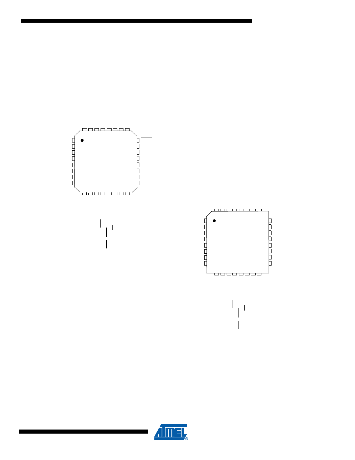
1. Pin Configurations
UVCC
QFN32
(PCINT11) PC2
(OC.0B / INT0) PD0
VCC
XTAL1
(INT5) PD4
(TXD1 / INT3) PD3
(XCK / PCINT12) PD5
PB3 (PDO / MISO / PCINT3)
GND
(PC0) XTAL2
UGND
PB4 (T1 / PCINT4)
2827 26
1
2
3
4
5
6
7
24
23
22
21
20
19
18
1211109131415
(AIN0 / INT1) PD1
8
16
17
PB6 (PCINT6)
D- / SDATA
D+ / SCK
2529303132
PB7 (PCINT7 / OC.0A / OC.1C)
PB5 (PCINT5)
PC7 (INT4 / ICP1 / CLKO)
PC6 (OC.1A / PCINT8)
Reset
(PC1 / dW)
PC5 ( PCINT9/ OC.1B)
PC4 (PCINT10)
UCAP
(RXD1 / AIN1 / INT2) PD2
(RTS / INT6) PD6
(CTS / HWB / T0 / INT7) PD7
(SS
/ PCINT0) PB0
(SCLK / PCINT1) PB1
(PDI / MOSI / PCINT2) PB2
AVCC
UVCC
VQFP32
(PCINT11) PC2
(OC.0B / INT0) PD0
VCC
XTAL1
(INT5) PD4
(TXD1 / INT3) PD3
(XCK / PCINT12) PD5
PB3 (PDO / MISO / PCINT3)
GND
(PC0) XTAL2
UGND
PB4 (T1 / PCINT4)
2827 26
1
2
3
4
5
6
7
24
23
22
21
20
19
18
1211109131415
(AIN0 / INT1) PD1
8
16
17
PB6 (PCINT6)
D- / SDATA
D+ / SCK
2529303132
PB7 (PCINT7 / OC.0A / OC.1C)
PB5 (PCINT5)
PC7 (INT4 / ICP1 / CLKO)
PC6 (OC.1A / PCINT8)
Reset
(PC1 / dW)
PC5 ( PCINT9/ OC.1B)
PC4 (PCINT10)
UCAP
(RXD1 / AIN1 / INT2) PD2
(RTS / INT6) PD6
(CTS / HWB / T0 / INT7) PD7
(SS
/ PCINT0) PB0
(SCLK / PCINT1) PB1
(PDI / MOSI / PCINT2) PB2
AVCC
Figure 1-1. Pinout AT90USB82/162
AT90USB82/162
1.1 Disclaimer
Note: The large center pad underneath the QFN packages is made of metal and must be connected to
GND. It should be sold ered or g lued to the boar d to ens ure good mech anica l st abili ty. If the c enter
pad is left unconnected, the package might loosen from the board.
Typical values contained in this datasheet are based on simulations and characterization of
other AVR microcontrollers manufactured on the same process technology. Min and Max values
will be available after the device is characterized.
7707DS–AVR–07/08
3
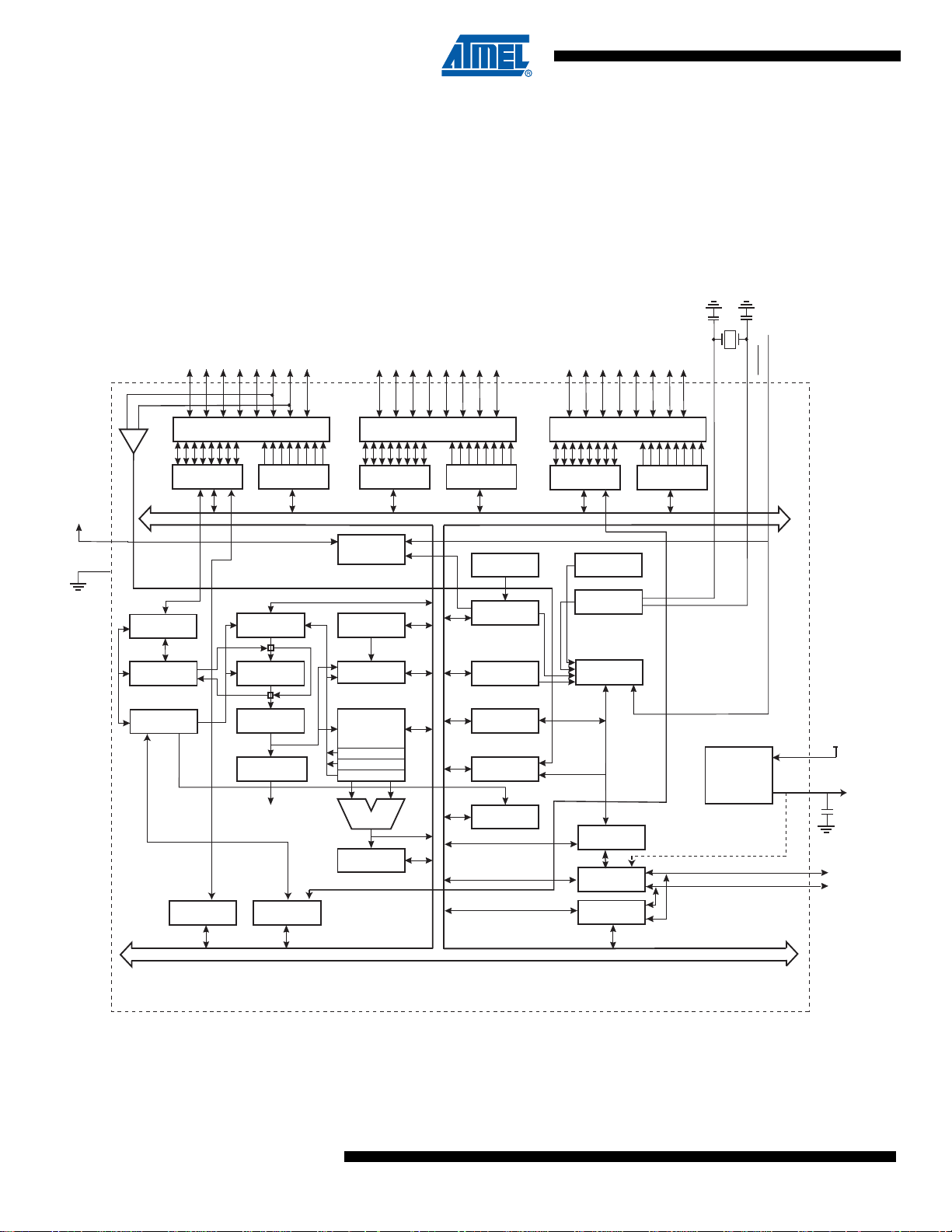
2. Overview
PROGRAM
COUNTER
STACK
POINTER
PROGRAM
FLASH
MCU CONTROL
REGISTER
SRAM
GENERAL
PURPOSE
REGISTERS
INSTRUCTION
REGISTER
TIMER/
COUNTERS
INSTRUCTION
DECODER
DATA DIR.
REG. PORTC
DATA REGISTER
PORTC
INTERRUPT
UNIT
EEPROM
USART1
STATUS
REGISTER
Z
Y
X
ALU
PORTC DRIVERS
PORTD DRIVERS
PORTB DRIVERS
PC7 - PC0 PD7 - PD0
RESET
VCC
GND
XTAL1
XTAL2
CONTROL
LINES
ANALOG
COMPARATOR
PB7 - PB0
D+/SCK
D-/SDATA
INTERNAL
OSCILLATOR
WATCHDOG
TIMER
8-BIT DA TA BUS
USB
PS/2
TIMING AND
CONTROL
OSCILLATOR
CALIB. OSC
DATA DIR.
REG. PORTB
DATA REGISTER
PORTB
ON-CHIP DEBUG
Debug-Wire
PROGRAMMING
LOGIC
DATA DIR.
REG. PORTD
DATA REGISTER
PORTD
POR - BOD
RESET
PLL
+
-
SPI
ON-CHIP
3.3V
REGULATOR
UVcc
UCap
1uF
The AT90USB82/162 is a low-power CMOS 8- bit micr ocon troller bas ed on th e AVR en hanced RISC ar chite cture. By executing powerful instructions in a single clock cycl e, the AT90USB82/162 ac hieves throughputs app roaching 1 MIPS per
MHz allowing the system designer to optimize power consumption versus processing speed.
2.1 Block Diagram
Figure 2-1. Block Diagram
The AVR core com bin es a rich instruction set with 32 general pur pos e worki ng regi ste rs . A ll the
32 registers are direc tly c onn ec ted to the Ari thme t ic Lo gi c Un it ( A LU), al lo wing two independent
registers to be accessed in one single instruction executed in one clock cycle. The resulting
4
AT90USB82/162
7707DS–AVR–07/08

AT90USB82/162
architecture is more code efficient while achieving throughputs up to ten times faster than conventional CISC microcontrollers.
The AT90USB82/162 pro vides the followi ng featu res: 8K / 16 K byte s of In-Sy stem Pr ogram mable Flash with Read-While-Write capabilities, 512 bytes EEPROM, 512 bytes SRAM, 22 general
purpose I/O lines , 32 gene ral purp ose work ing reg isters , two flex ible Time r/Coun ters with compare modes and PWM, one USART, a programmable Watchdog Timer with Internal Oscillator,
an SPI serial port, debugW IRE interface, als o used for access ing the On-chip Deb ug system
and programming and five software selectable power saving modes. Th e Idle mode stops the
CPU while allowing the SRAM, Timer/Counters, SPI port, and interrupt system to continue functioning. The Power-do wn mode sav es the registe r content s but freezes the Oscil lator, disa bling
all other chip functions until the next interrupt or Hardware Reset. In Standby mode, the Crystal/Resonator Oscillator is running while the rest of the device is sleeping. This allows very fast
start-up combined wit h low power co ns ump tio n. In E xte nde d Sta ndb y mo de, the main Oscillator
continues to run.
The device is manufac ture d using Atmel’s high-density nonv ol atil e me mory tec hno log y. Th e onchip ISP Flash allows the program memory to be reprogrammed in-system through an SPI serial
interface, by a conventi onal nonvola tile memory progr ammer, or by an on-chi p Boot program
running on the AVR core. The boot program can use any interface to download the application
program in the application Flash memory. Software in the Boot Flash section will continue to run
while the Application Flash section is updated, prov iding true Read-Whi le-Write operation. By
combining an 8-bit RISC CP U with In-System Self-Programm able Flash on a monolithi c chip,
the Atmel AT90US B82/ 162 i s a powerful mic rocon troller tha t pr ovides a hi ghly flexi ble a nd c ost
effective solution to many embedded control applications.
The AT90USB82/162 AVR is supported with a full suite of program and system develop ment
tools including: C co mpile rs, m acro as sembl ers, pr ogram deb ugg er/simu lator s, in-c ircuit e mulators, and evaluation kits.
2.2 Pin Descriptions
2.2.1 VCC
Digital supply voltage.
2.2.2 GND
Ground.
2.2.3 Port B (PB7..PB0)
Port B is an 8-bi t b i- dire ctional I/O port with in terna l pul l- up res ist ors (se le cte d f or ea ch bi t). T h e
Port B output buffers have symmetrical drive characteristics with both high sink and source
capability. As inputs, Port B pins that are externally pulled low will source current if the pull-up
resistors are activated. The Port B pins are tri-stated whe n a rese t condition bec omes activ e,
even if the clock is not running.
Port B also ser ves th e f unctions of variou s spec ial featu res of the A T90USB 82/16 2 as listed o n
page 74.
7707DS–AVR–07/08
5

2.2.4 Port C (PC7..PC0)
Port C is an 8-bit bi- dire ct ion al I/O po rt with in ter na l p ull- up r esi sto rs ( s ele ct ed fo r eac h b it). T h e
Port C output buffers have symmetrical drive characteristics with both high sink and source
capability. As inputs, Port C pins that are externally pulled low will source current if the pull-up
resistors are activated. The Port C pi ns are tri-stated when a res et condition bec omes active,
even if the clock is not running.
Port C also serves the function s of various spe cial features of the AT 90USB82 /162 as liste d on
page 76.
2.2.5 Port D (PD7..PD0)
Port D serves as analog inputs to the analog comparator.
Port D also serves as an 8-bit bi-directional I/O port, if the analog comparator is not used (con-
cerns PD2/PD1 pins). Port pins can provide internal pull-up resistors (selected for each bit). The
Port D output buffers have symmetrical drive characteristics with both high sink and source
capability. As inputs, Port D pins that are externally pulled low will source current if the pull-up
resistors are activated. The Port D pi ns are tri-stated when a res et condition bec omes active,
even if the clock is not running.
2.2.6 D-/SDATA
USB Full Speed Negative Data Upstream Port / Data port for PS/2
2.2.7 D+/SCK
USB Full Speed Positive Data Upstream Port / Clock port for PS/2
2.2.8 UGND
2.2.9 UVCC
2.2.10 UCAP
2.2.11 RESET/PC1/dW
2.2.12 XTAL1
2.2.13 XTAL2/PC0
USB Ground.
USB Pads Internal Regulator Input supply voltage.
USB Pads Internal Regulator Output supply voltage. Should be connected to an external capacitor (1µF).
Reset input. A low level on this pin for longer than the minimum pulse length will generate a
reset, even if the clock is not runni ng. The minim um pulse l ength is given in Section 9.. Shorter
pulses are not guaranteed to generate a reset. This pin alternatively serves as debugWire channel or as generic I/O. The configuration depends on the fuses RSTDISBL and DWEN.
Input to the inverting Oscillator amplifier and input to the internal clock operating circuit.
Output from the inverting Oscillator amplifier if enabled by Fuse. Also serves as a generic I/O.
6
AT90USB82/162
7707DS–AVR–07/08

3. About Code Examples
This documentation contains simple code examples that briefly show how to use various parts of
the device. Be aware that not all C c ompiler ven dors inc lude bit defini tions in th e header files
and interrupt handling in C is compiler dependent. Please confirm with the C compiler documentation for more details.
These code examples assume that the part specific header file is included before compilation.
For I/O registers located in extended I/O map, "IN", "OUT", "SBIS", "SBIC", "CBI", and "SBI"
instructions must be replace d with instruc tions that al low access to extended I/O . Typically
"LDS" and "STS" combined with "SBRS", "SBRC", "SBR", and "CBR".
AT90USB82/162
7707DS–AVR–07/08
7

4. Register Summary
Address Name Bit 7 Bit 6 Bit 5 Bit 4 Bit 3 Bit 2 Bit 1 Bit 0 Page
(0xFF) Reserved - - - - - - - (0xFE) Reserved - - - - - - - (0xFD) Reserved - - - - - - - (0xFC) Reserved - - - - - - - (0xFB) UPOE UPWE1 UPWE0 UPDRV1 UPDRV0 SCKI DATAI DPI DMI
(0xFA) PS2CON - - - - - - - PS2EN
(0xF9) Reserved - - - - - - - (0xF8) Reserved - - - - - - - (0xF7) Reserved - - - - - - - (0xF6) Reserved - - - - - - - (0xF5) Reserved
(0xF4) UEINT
(0xF3) Reserved - - - - - - - (0xF2) UEBCLX BYCT7:0
(0xF1) UEDATX DAT7:0
(0xF0) UEIENX FLERRE NAKINE - NAKOUTE RXSTPE RXOUTE STALLEDE TXINE
(0xEF) UESTA1X
(0xEE) UESTA0X CFGOK OVERFI UNDERFI
(0xED) UECFG1X - EPSIZE2:0 EPBK1:0 ALLOC (0xEC) UECFG0X EPTYPE1:0 - - - - -EPDIR
(0xEB) UECONX - - STALLRQ STALLRQC RSTDT - - EPEN
(0xEA) UERST - - -EPRST4:0
(0xE9) UENUM - - - - - EPNUM2:0
(0xE8) UEINTX FIFOCON NAKINI RWAL NAKOUTI RXSTPI RXOUTI STALLEDI TXINI
(0xE7) Reserved - - - - - - - -
(0xE6) UDMFN - - - FNCERR - - - -
(0xE5) UDFNUMH - - - - - FNUM10:8
(0xE4) UDFNUML FNUM7:0
(0xE3) UDADDR ADDEN UADD6:0
(0xE2) UDIEN - UPRSME EORSME WAKEUPE EORSTE SOFE -SUSPE
(0xE1) UDINT - UPRSMI EORSMI WAKEUPI EORSTI SOFI -SUSPI
(0xE0) UDCON - - - - - RSTCPU RMWKUP DETACH
(0xDF) Reserved - - - - - - - (0xDE) Reserved - - - - - - - (0xDD) Reserved - - - - - - - (0xDC) Reserved - - - - - - - (0xDB) Reserved - - - - - - - (0xDA) Reserved - - - - - - - -
(0xD9) Reserved - - - - - - - -
(0xD8) USBCON USBE - FRZCLK - - - - -
(0xD7) Reserved - - - - - - - -
(0xD6) Reserved - - - - - - - -
(0xD5) Reserved - - - - - - - -
(0xD4) Reserved
(0xD3) Reserved
(0xD2) CLKSTA - - - - - -RCONEXTON
(0xD1) CLKSEL1 RCCKSEL3 RCCKSEL2 RCCKSEL1 RCCKSEL0 EXCKSEL3 EXCKSEL2 EXCKSEL1 EXCKSEL0
(0xD0) CLKSEL0 RCSUT1 RCSUT0 EXSUT1 EXSUT0 RCE EXTE -CLKS
(0xCF) Reserved
(0xCE) UDR1 USART1 I/O Data Register
(0xCD) UBRR1H
(0xCC) UBRR1L USART1 Baud Rate Register Low Byte
(0xCB) UCSR1D - - - - - - CTSEN RTSEN
(0xCA) UCSR1C UMSEL11 UMSEL10 UPM11 UPM10 USBS1 UCSZ11 UCSZ10 UCPOL1
(0xC9) UCSR1B RXCIE1 TXCIE1 UDRIE1 RXEN1 TXEN1 UCSZ12 RXB81 TXB81
(0xC8) UCSR1A RXC1 TXC1 UDRE1 FE1 DOR1 PE1 U2X1 MPCM1
(0xC7) Reserved - - - - - - - -
(0xC6) Reserved - - - - - - - -
(0xC5) Reserved
(0xC4) Reserved
(0xC3) Reserved - - - - - - - -
(0xC2) Reserved
(0xC1) Reserved
(0xC0) Reserved - - - - - - - -
(0xBF) Reserved
- - - - - - - -
- -EPINT4:0
- - - - - CTRLDIR CURRBK1:0
- DTSEQ1:0 NBUSYBK1:0
- - - - - - - -
- - - - - - - -
- - - - - - - -
- - - - USART1 Baud Rate Register High Byte
- - - - - - - -
- - - - - - - -
- - - - - - - -
- - - - - - - -
- - - - - - - -
8
AT90USB82/162
7707DS–AVR–07/08

AT90USB82/162
Address Name Bit 7 Bit 6 Bit 5 Bit 4 Bit 3 Bit 2 Bit 1 Bit 0 Page
(0xBE) Reserved - - - - - - - (0xBD) Reserved - - - - - - - (0xBC) Reserved - - - - - - - -
(0xBB) Reserved - - - - - - - -
(0xBA) Reserved - - - - - - - -
(0xB9) Reserved
(0xB8) Reserved
(0xB7) Reserved - - - - - - - -
(0xB6) Reserved
(0xB5) Reserved
(0xB4) Reserved - - - - - - - -
(0xB3) Reserved - - - - - - - -
(0xB2) Reserved - - - - - - - -
(0xB1) Reserved - - - - - - - -
(0xB0) Reserved - - - - - - - -
(0xAF) Reserved - - - - - - - -
(0xAE) Reserved - - - - - - - (0xAD) Reserved
(0xAC) Reserved
(0xAB) Reserved - - - - - - - -
(0xAA) Reserved - - - - - - - -
(0xA9) Reserved - - - - - - - -
(0xA8) Reserved - - - - - - - -
(0xA7) Reserved - - - - - - - -
(0xA6) Reserved - - - - - - - -
(0xA5) Reserved - - - - - - - -
(0xA4) Reserved - - - - - - - -
(0xA3) Reserved - - - - - - - -
(0xA2) Reserved - - - - - - - -
(0xA1) Reserved - - - - - - - -
(0xA0) Reserved - - - - - - - -
(0x9F) Reserved - - - - - - - -
(0x9E) Reserved - - - - - - - -
(0x9D) Reserved - - - - - - - -
(0x9C) Reserved - - - - - - - -
(0x9B) Reserved - - - - - - - -
(0x9A) Reserved - - - - - - - -
(0x99) Reserved - - - - - - - -
(0x98) Reserved - - - - - - - -
(0x97) Reserved - - - - - - - -
(0x96) Reserved - - - - - - - -
(0x95) Reserved - - - - - - - -
(0x94) Reserved - - - - - - - -
(0x93) Reserved - - - - - - - -
(0x92) Reserved
(0x91) Reserved
(0x90) Reserved - - - - - - - -
(0x8F) Reserved
(0x8E) Reserved
(0x8D) OCR1CH Timer/Counter1 - Output Compare Register C High Byte
(0x8C) OCR1CL Timer/Counter1 - Output Compare Register C Low Byte
(0x8B) OCR1BH Timer/Counter1 - Output Compare Register B High Byte
(0x8A) OCR1BL Timer/Counter1 - Output Compare Register B Low Byte
(0x89) OCR1AH Timer/Counter1 - Output Compare Register A High Byte
(0x88) OCR1AL Timer/Counter1 - Output Compare Register A Low Byte
(0x87) ICR1H Timer/Counter1 - Input Capture Register High Byte
(0x86) ICR1L Timer/Counter1 - Input Capture Register Low Byte
(0x85) TCNT1H Timer/Counter1 - Counter Register High Byte
(0x84) TCNT1L Timer/Counter1 - Counter Register Low Byte
(0x83) Reserved
(0x82) TCCR1C FOC1A FOC1B FOC1C
(0x81) TCCR1B ICNC1 ICES1 - WGM13 WGM12 CS12 CS11 CS10
(0x80) TCCR1A COM1A1 COM1A0 COM1B1 COM1B0 COM1C1 COM1C0 WGM11 WGM10
(0x7F) Reserved - - - - - - - -
(0x7E) Reserved - - - - - - - -
(0x7D) Reserved
- - - - - - - -
- - - - - - - -
- - - - - - - -
- - - - - - - -
- - - - - - - -
- - - - - - - -
- - - - - - - -
- - - - - - - -
- - - - - - - -
- - - - - - - -
- - - - - - - -
- - - - -
- - - - - - - -
7707DS–AVR–07/08
9

Address Name Bit 7 Bit 6 Bit 5 Bit 4 Bit 3 Bit 2 Bit 1 Bit 0 Page
(0x7C) Reserved - - - - - - - -
(0x7B) Reserved - - - - - - - -
(0x7A) Reserved - - - - - - - -
(0x79) Reserved - - - - - - - -
(0x78) Reserved - - - - - - - -
(0x77) Reserved
(0x76) Reserved
(0x75) Reserved - - - - - - - -
(0x74) Reserved
(0x73) Reserved
(0x72) Reserved - - - - - - - -
(0x71) Reserved - - - - - - - -
(0x70) Reserved - - - - - - - -
(0x6F) TIMSK1 - -ICIE1- OCIE1C OCIE1B OCIE1A TOIE1
(0x6E) TIMSK0 - - - - - OCIE0B OCIE0A TOIE0
(0x6D) Reserved - - - - - - - -
(0x6C) PCMSK1 - - - PCINT12 PCINT11 PCINT10 PCINT9 PCINT8
(0x6B) PCMSK0 PCINT7 PCINT6 PCINT5 PCINT4 PCINT3 PCINT2 PCINT1 PCINT0
(0x6A) EICRB ISC71 ISC70 ISC61 ISC60 ISC51 ISC50 ISC41 ISC40
(0x69) EICRA ISC31 ISC30 ISC21 ISC20 ISC11 ISC10 ISC01 ISC00
(0x68) PCICR - - - - - -PCIE1PCIE0
(0x67) Reserved - - - - - - - -
(0x66) OSCCAL Oscillator Calibration Register
(0x65) PRR1 PRUSB - - - - - - PRUSART1
(0x64) PRR0 - -PRTIM0-PRTIM1PRSPI - -
(0x63) REGCR - - - - - - -REGDIS
(0x62) WDTCKD - - - - WDEWIF WDEWIE WCLKD1 WCLKD0
(0x61) CLKPR CLKPCE - - - CLKPS3 CLKPS2 CLKPS1 CLKPS0
(0x60) WDTCSR WDIF WDIE WDP3 WDCE WDE WDP2 WDP1 WDP0
0x3F (0x5F) SREG I T H S V N Z C
0x3E (0x5E) SPH SP15 SP14 SP13 SP12 SP11 SP10 SP9 SP8
0x3D (0x5D) SPL SP7 SP6 SP5 SP4 SP3 SP2 SP1 SP0
0x3C (0x5C) Reserved - - - - - - - 0x3B (0x5B) Reserved - - - - - - - 0x3A (0x5A) Reserved - - - - - - - -
0x39 (0x59) Reserved - - - - - - - -
0x38 (0x58) Reserved - - - - - - - -
0x37 (0x57) SPMCSR SPMIE RWWSB SIGRD RWWSRE BLBSET PGWRT PGERS SPMEN
0x36 (0x56) Reserved - - - - - - - -
0x35 (0x55) MCUCR - - - - - - IVSEL IVCE
0x34 (0x54) MCUSR - -USBRF- WDRF BORF EXTRF PORF
0x33 (0x53) SMCR - - - -SM2SM1SM0SE
0x32 (0x52) Reserved - - - - - - - -
0x31 (0x51) DWDR debugWIRE Data Register
0x30 (0x50) ACSR ACD ACBG ACO ACI ACIE ACIC ACIS1 ACIS0
0x2F (0x4F) Reserved - - - - - - - 0x2E (0x4E) SPDR SPI Data Register
0x2D (0x4D) SPSR SPIF WCOL
0x2C (0x4C) SPCR SPIE SPE DORD MSTR CPOL CPHA SPR1 SPR0
0x2B (0x4B) GPIOR2 General Purpose I/O Register 2
0x2A (0x4A) GPIOR1 General Purpose I/O Register 1
0x29 (0x49) PLLCSR
0x28 (0x48) OCR0B Timer/Counter0 Output Compare Register B
0x27 (0x47) OCR0A Timer/Counter0 Output Compare Register A
0x26 (0x46) TCNT0 Timer/Counter0 (8 Bit)
0x25 (0x45) TCCR0B FOC0A FOC0B - - WGM02 CS02 CS01 CS00
0x24 (0x44) TCCR0A COM0A1 COM0A0 COM0B1 COM0B0 - -WGM01WGM00
0x23 (0x43) GTCCR TSM - - - - - PSRASY PSRSYNC
0x22 (0x42) EEARH
0x21 (0x41) EEARL EEPROM Address Register Low Byte
0x20 (0x40) EEDR EEPROM Data Register
0x1F (0x3F) EECR
0x1E (0x3E) GPIOR0 General Purpose I/O Register 0
0x1D (0x3D) EIMSK INT7 INT6 INT5 INT4 INT3 INT2 INT1 INT0
0x1C (0x3C) EIFR INTF7 INTF6 INTF5 INTF4 INTF3 INTF2 INTF1 INTF0
0x1B (0x3B) PCIFR
- - - - - - - -
- - - - - - - -
- - - - - - - -
- - - - - - - -
- - - - - SPI2X
- - - PLLP2 PLLP1 PLLP0 PLLE PLOCK
- - - - EEPROM Address Register High Byte
- - EEPM1 EEPM0 EERIE EEMPE EEPE EERE
- - - - - -PCIF1PCIF0
10
AT90USB82/162
7707DS–AVR–07/08

AT90USB82/162
Address Name Bit 7 Bit 6 Bit 5 Bit 4 Bit 3 Bit 2 Bit 1 Bit 0 Page
0x1A (0x3A) Reserved - - - - - - - -
0x19 (0x39) Reserved - - - - - - - -
0x18 (0x38) Reserved - - - - - - - -
0x17 (0x37) Reserved - - - - - - - -
0x16 (0x36) TIFR1 - -ICF1- OCF1C OCF1B OCF1A TOV1
0x15 (0x35) TIFR0
0x14 (0x34) Reserved
0x13 (0x33) Reserved - - - - - - - -
0x12 (0x32) Reserved
0x11 (0x31) Reserved
0x10 (0x30) Reserved - - - - - - - 0x0F (0x2F) Reserved - - - - - - - 0x0E (0x2E) Reserved - - - - - - - 0x0D (0x2D) Reserved - - - - - - - 0x0C (0x2C) Reserved - - - - - - - 0x0B (0x2B) PORTD PORTD7 PORTD6 PORTD5 PORTD4 PORTD3 PORTD2 PORTD1 PORTD0
0x0A (0x2A) DDRD DDD7 DDD6 DDD5 DDD4 DDD3 DDD2 DDD1 DDD0
0x09 (0x29) PIND PIND7 PIND6 PIND5 PIND4 PIND3 PIND2 PIND1 PIND0
0x08 (0x28) PORTC PORTC7 P ORTC6 PORTC5 PORTC4 - PORTC2 PORTC1 PORTC0
0x07 (0x27) DDRC DDC7 DDC6 DDC5 DDC4 - DDC2 DDC1 DDC0
0x06 (0x26) PINC PINC7 PINC6 PINC5 PINC4 - PINC2 PINC1 PINC0
0x05 (0x25) PORTB PORTB7 PORTB6 PORTB5 PORTB4 PORTB3 PORTB2 PORTB1 PORTB0
0x04 (0x24) DDRB DDB7 DDB6 DDB5 DDB4 DDB3 DDB2 DDB1 DDB0
0x03 (0x23) PINB PINB7 PINB6 PINB5 PINB4 PINB3 PINB2 PINB1 PINB0
0x02 (0x22) Reserved - - - - - - - -
0x01 (0x21) Reserved - - - - - - - -
0x00 (0x20) Reserved - - - - - - - -
Note: 1. For compatibility with future devices, reserved bits should be written to zero if accessed. Moreover reserved bits are not
guaranteed to be read as “0”. Reserved I/O memory addresses should never be written.
2. I/O registers within the address range $00 - $1F are directly bit-accessible using the SBI and CBI instructions. In these registers, the value of single bits can be checked by using the SBIS and SBIC instructions.
3. Some of the status flags are cleared by writing a logical one to them. Note that the CBI and SBI instructions will operate on
all bits in the I/O register, writing a one back into any flag read as set, thus clearing the flag. The CBI and SBI instructions
work with registers 0x00 to 0x1F only.
4. When using the I/O specific commands IN and OUT, the I/O addresses $00 - $3F must be used. When addressing I/O registers as data space using LD and ST instructions, $20 must be added to these addresses. The AT90USB82/162 is a
complex microcontroller with more peripheral units than can be supported within the 64 location reserved in Opcode for the
IN and OUT instructions. For the Extended I/O space from $60 - $1FF in SRAM, only the ST/STS/STD and LD/LDS/LDD
instructions can be used.
- - - - - OCF0B OCF0A TOV0
- - - - - - - -
- - - - - - - -
- - - - - - - -
7707DS–AVR–07/08
11

5. Instruction Set Summary
Mnemonics Operands Description Operation Flags #Clocks
ADD Rd, Rr Add two Registers Rd ← Rd + Rr Z,C,N,V,H 1
ADC Rd, Rr Add with Carry two Registers Rd ← Rd + Rr + C Z,C,N,V,H 1
ADIW Rdl,K Add Immediate to Word Rdh:Rdl ← Rdh:Rdl + K Z,C,N,V,S 2
SUB Rd, Rr Subtract two Registers Rd ← Rd - Rr Z,C,N,V,H 1
SUBI Rd, K Subtract Constant from Register Rd ← Rd - K Z,C,N,V,H 1
SBC Rd, Rr Subtract with Carry two Registers Rd ← Rd - Rr - C Z,C,N,V,H 1
SBCI Rd, K Subtract with Carry Constant from Reg. Rd ← Rd - K - C Z,C,N,V,H 1
SBIW Rdl,K Subtract Immediate from Word Rdh:Rdl ← Rdh:Rdl - K Z,C,N,V,S 2
AND Rd, Rr Logical AND Registers Rd ← Rd • Rr Z,N,V 1
ANDI Rd, K Logical AND Register and Constant Rd ← Rd • K Z,N,V 1
OR Rd, Rr Logical OR Registers Rd ← Rd v Rr Z,N,V 1
ORI Rd, K Logical OR Register and Constant Rd ← Rd v K Z,N,V 1
EOR Rd, Rr Exclusive OR Registers Rd ← Rd ⊕ Rr Z,N,V 1
COM Rd One’s Complement Rd ← 0xFF − Rd Z,C,N,V 1
NEG Rd Two’s Complement Rd ← 0x00 − Rd Z,C,N,V,H 1
SBR Rd,K Set Bit(s) in Register Rd ← Rd v K Z,N,V 1
CBR Rd,K Clear Bit(s) in Register Rd ← Rd • (0xFF - K) Z,N,V 1
INC Rd Increment Rd ← Rd + 1 Z,N,V 1
DEC Rd Decrement Rd ← Rd − 1 Z,N,V 1
TST Rd Test for Zero or Minus Rd ← Rd • Rd Z,N,V 1
CLR Rd Clear Register Rd ← Rd ⊕ Rd Z,N,V 1
SER Rd Set Register Rd ← 0xFF None 1
RJMP k Relative Jump PC ← PC + k + 1 None 2
IJMP Indirect Jump to (Z) PC ← Z None 2
JMP k Direct Jump PC ← k None 3
RCALL k Relative Subroutine Call PC ← PC + k + 1 None 4
ICALL Indirect Call to (Z) PC ← Z None 4
CALL k Direct Subroutine Call PC ← k None 5
RET Subroutine Return PC ← STACK None 5
RETI Interrupt Return PC ← STACK I 5
CPSE Rd,Rr Compare, Skip if Equal if (Rd = Rr) PC ← PC + 2 or 3 None 1/2/3
CP Rd,Rr Compare Rd − Rr Z, N,V,C,H 1
CPC Rd,Rr Compare with Carry Rd − Rr − CZ, N,V,C,H1
CPI Rd,K Compare Register with Immediate Rd − K Z, N,V,C,H 1
SBRC Rr, b Skip if Bit in Register Cleared if (Rr(b)=0) PC ← PC + 2 or 3 None 1/2/3
SBRS Rr, b Skip if Bit in Register is Set if (Rr(b)=1) PC ← PC + 2 or 3 None 1/2/3
SBIC P, b Skip if Bit in I/O Register Cleared if (P(b)=0) PC ← PC + 2 or 3 None 1/2/3
SBIS P, b Skip if Bit in I/O Register is Set if (P(b)=1) PC ← PC + 2 or 3 None 1/2/3
BRBS s, k Branch if Status Flag Set if (SREG(s) = 1) then PC←PC+k + 1 None 1/2
BRBC s, k Branch if Status Flag Cleared if (SREG(s) = 0) then PC←PC+k + 1 None 1/2
BREQ k Branch if Equal if (Z = 1) then PC ← PC + k + 1 None 1/2
BRNE k Branch if Not Equal if (Z = 0) then PC ← PC + k + 1 None 1/2
BRCS k Branch if Carry Set if (C = 1) then PC ← PC + k + 1 None 1/2
BRCC k Branch if Carry Cleared if (C = 0) then PC ← PC + k + 1 None 1/2
BRSH k Branch if Same or Higher if (C = 0) then PC ← PC + k + 1 None 1/2
BRLO k Branch if Lower if (C = 1) then PC ← PC + k + 1 None 1/2
BRMI k Branch if Minus if (N = 1) then PC ← PC + k + 1 None 1/2
BRPL k Branch if Plus if (N = 0) then PC ← PC + k + 1 None 1/2
BRGE k Branch if Greater or Equal, Signed if (N ⊕ V= 0) then PC ← PC + k + 1 None 1/2
BRLT k Branch if Less Than Zero, Signed if (N ⊕ V= 1) then PC ← PC + k + 1 None 1/2
BRHS k Branch if Half Carry Flag Set if (H = 1) then PC ← PC + k + 1 None 1/2
BRHC k Branch if Half Carry Flag Cleared if (H = 0) then PC ← PC + k + 1 None 1/2
BRTS k Branch if T Flag Set if (T = 1) then PC ← PC + k + 1 None 1/2
BRTC k Branch if T Flag Cleared if (T = 0) then PC ← PC + k + 1 None 1/2
BRVS k Branch if Overflow Flag is Set if (V = 1) then PC ← PC + k + 1 None 1/2
BRVC k Branch if Overflow Flag is Cleared if (V = 0) then PC ← PC + k + 1 None 1/2
BRIE k Branch if Interrupt Enabled if ( I = 1) then PC ← PC + k + 1 None 1/2
BRID k Branch if Interrupt Disabled if ( I = 0) then PC ← PC + k + 1 None 1/2
SBI P,b Set Bit in I/O Register I/O(P,b)
CBI P,b Clear Bit in I/O Register I/O(P,b) ← 0 None 2
LSL Rd Logical Shift Left Rd(n+1) ← Rd(n), Rd(0) ← 0 Z,C,N,V 1
LSR Rd Logical Shift Right Rd(n) ← Rd(n+1), Rd(7) ← 0 Z,C,N,V 1
ARITHMETIC AND LOGIC INSTRUCTIONS
BRANCH INSTRUCTIONS
BIT AND BIT-TEST INSTRUCTIONS
← 1 None 2
12
AT90USB82/162
7707DS–AVR–07/08

AT90USB82/162
Mnemonics Operands Description Operation Flags #Clocks
ROL Rd Rotate Left Through Carry Rd(0)←C,Rd(n+1)← Rd(n),C←Rd(7) Z,C,N,V 1
ROR Rd Rotate Right Through Carry Rd(7)←C,Rd(n)← Rd(n+1),C←Rd(0) Z,C,N,V 1
ASR Rd Arithmetic Shift Right Rd(n) ← Rd(n+1), n=0..6 Z,C,N,V 1
SWAP Rd Swap Nibbles Rd(3..0)←Rd(7..4),Rd(7..4)←Rd(3..0) None 1
BSET s Flag Set SREG(s) ← 1 SREG(s) 1
BCLR s Flag Clear SREG(s) ← 0 SREG(s) 1
BST Rr, b Bit Store from Register to T T ← Rr(b) T 1
BLD Rd, b Bit load from T to Register Rd(b) ← T None 1
SEC Set Carry C ← 1C1
CLC Clear Carry C ← 0 C 1
SEN Set Negative Flag N ← 1N1
CLN Clear Negative Flag N ← 0 N 1
SEZ Set Zero Flag Z ← 1Z1
CLZ Clear Zero Flag Z ← 0 Z 1
SEI Global Interrupt Enable I ← 1I1
CLI Global Interrupt Disable I ← 0 I 1
SES Set Signed Test Flag S ← 1S1
CLS Clear Signed Test Flag S ← 0 S 1
SEV Set Twos Complement Overflow. V ← 1V1
CLV Clear Twos Complement Overflow V ← 0 V 1
SET Set T in SREG T ← 1T1
CLT Clear T in SREG T ← 0 T 1
SEH Set Half Carry Flag in SREG H ← 1H1
CLH Clear Half Carry Flag in SREG H ← 0 H 1
MOV Rd, Rr Move Between Registers Rd ← Rr None 1
MOVW Rd, Rr Copy Register Word
LDI Rd, K Load Immediate Rd ← K None 1
LD Rd, X Load Indirect Rd ← (X) None 2
LD Rd, X+ Load Indirect and Post-Inc. Rd ← (X), X ← X + 1 None 2
LD Rd, - X Load Indirect and Pre-Dec. X ← X - 1, Rd ← (X) None 2
LD Rd, Y Load Indirect Rd ← (Y) None 2
LD Rd, Y+ Load Indirect and Post-Inc. Rd ← (Y), Y ← Y + 1 None 2
LD Rd, - Y Load Indirect and Pre-Dec. Y ← Y - 1, Rd ← (Y) None 2
LDD Rd,Y+q Load Indirect with Displacement Rd ← (Y + q) None 2
LD Rd, Z Load Indirect Rd ← (Z) None 2
LD Rd, Z+ Load Indirect and Post-Inc. Rd ← (Z), Z ← Z+1 None 2
LD Rd, -Z Load Indirect and Pre-Dec. Z ← Z - 1, Rd ← (Z) None 2
LDD Rd, Z+q Load Indirect with Displacement Rd ← (Z + q) None 2
LDS Rd, k Load Direct from SRAM Rd ← (k) None 2
ST X, Rr Store Indirect (X) ← Rr None 2
ST X+, Rr Store Indirect and Post-Inc. (X) ← Rr, X ← X + 1 None 2
ST - X, Rr Store Indirect and Pre-Dec. X ← X - 1, (X) ← Rr None 2
ST Y, Rr Store Indirect (Y) ← Rr None 2
ST Y+, Rr Store Indirect and Post-Inc. (Y) ← Rr, Y ← Y + 1 None 2
ST - Y, Rr Store Indirect and Pre-Dec. Y ← Y - 1, (Y) ← Rr None 2
STD Y+q,Rr Store Indirect with Displacement (Y + q) ← Rr None 2
ST Z, Rr Store Indirect (Z) ← Rr None 2
ST Z+, Rr Store Indirect and Post-Inc. (Z) ← Rr, Z ← Z + 1 None 2
ST -Z, Rr Store Indirect and Pre-Dec. Z ← Z - 1, (Z) ← Rr None 2
STD Z+q,Rr Store Indirect with Displacement (Z + q) ← Rr None 2
STS k, Rr Store Direct to SRAM (k) ← Rr None 2
LPM Load Program Memory R0 ← (Z) None 3
LPM Rd, Z Load Program Memory Rd ← (Z) None 3
LPM Rd, Z+ Load Program Memory and Post-Inc Rd ← (Z), Z ← Z+1 None 3
SPM Store Program Memory (Z)
IN Rd, P In Port Rd ← P None 1
OUT P, Rr Out Port P ← Rr None 1
PUSH Rr Push Register on Stack STACK ← Rr None 2
POP Rd Pop Register from Stack Rd ← STACK None 2
NOP No Operation None 1
SLEEP Sleep (see specific descr. for Sleep function) None 1
WDR Watchdog Reset (see specific descr. for WDR/timer) None 1
BREAK Break For On-chip Debug Only None N/A
DATA TRANSFER INSTRUCTIONS
MCU CONTROL INSTRUCTIONS
Rd+1:Rd ← Rr+1:Rr
← R1:R0 None -
None 1
7707DS–AVR–07/08
13

6. Ordering Information
Part Number Temp. Range Flash Memory Size Package Product Marking
90USB82-16MU Industrial Green 8K QFN32 90USB82-16MU
90USB162-16MU Industrial Green 16K QFN32 90USB162-16MU
90USB162-16AU Industrial Green 16K TQFP32 90USB162-16AU
7. Packaging Information
PN, 32-Lead 5.0 x 5.0 mm Body, 0.50 mm Pitch
QFN32
TQFP32
14
Quad Flat No Lead Package (QFN)
MA, 32-Lead 7 x 7 mm Body size, 1.00 mm Bodu Thickness
0.5 mm Lead Pitch, Thin Profile Plastic Quad Flat Package (TQFP)
AT90USB82/162
Package Type
7707DS–AVR–07/08

7.1 QFN32
*
AT90USB82/162
7707DS–AVR–07/08
15

7.2 TQFP32
16
AT90USB82/162
7707DS–AVR–07/08

8. Errata
8.1 AT90USB1 62 Erra ta History
AT90USB82/162
Silicon
Release
First Release
Second Release ‘0709 F3150-1’
Third Release All date codes after 0709 All other lots
8.1.1 AT90USB162 First Release
1. High current consumption in sleep mode
If a pending interrupt cannot wake the part up from the selected mode, the current consumption will increase during sleep when executing the SLEEP instruction directly after a SEI
instruction.
Problem Fix/workaround
Before entering sleep, interrupts not used to wake up the part from the sleep mode should
be disabled.
2. PS2 high level clamped to UCAP
When configured in PS2 mode, the output high level is clamped to the UCAP voltage level.
QFP32
‘DateCode LotNumber’ marking
‘0705 6J4972’
‘0709 J4973-2’
‘0709 J5597-1’
QFN32
‘DateCode LotNumber’ marking
all lots marked
90USB162–16MES
‘0714 50-2’
‘0722 50-3’
‘0735 3151’
Problem Fix/workaround
None.
3. Transient perturbation in USB suspend mode generates overconsumption
In device mode and when the USB is suspended, transient perturbation received on the
USB lines generates a wake up state. However the idle state following the perturbation does
not set the SUSPI bi t anymore . The int ernal USB engine rem ains in suspend mo de but the
USB differential receiver is still enabled and generates a typical 300µA extra-power consumption. Detection of the s uspend state after the transient p erturbation should be
performed by software (instead of reading the SUS PI bit ).
Problem fix/workaround
USB waiver allows bus powered devices to consume up to 2.5mA in suspend state.
8.1.2 AT90USB162 Second Release
1. High current consumption in sleep mode
If a pending interrupt cannot wake the part up from the selected mode, the current consumption will increase during sleep when executing the SLEEP instruction directly after a SEI
instruction.
Problem Fix/workaround
7707DS–AVR–07/08
17

Before entering sleep, interrupts not used to wake up the part from the sleep mode should
be disabled.
2. Extra power consumption
The typical power comsumption is increased by 90µA at 5V and by 160µA in worst case
conditions.
Problem Fix/workaround
None.
3. Transient perturbation in USB suspend mode generates overconsumption
In device mode and when the USB is suspended, transient perturbation received on the
USB lines generates a wake up state. However the idle state following the perturbation does
not set the SUSPI bi t anymore . The int ernal USB engine rem ains in suspend mo de but the
USB differential receiver is still enabled and generates a typical 300µA extra-power consumption. Detection of the s uspend state after the transient p erturbation should be
performed by software (instead of reading the SUS PI bit ).
Problem fix/workaround
USB waiver allows bus powered devices to consume up to 2.5mA in suspend state.
8.1.3 AT90USB162 Third Release
1. High current consumption in sleep mode
If a pending interrupt cannot wake the part up from the selected mode, the current consumption will increase during sleep when executing the SLEEP instruction directly after a SEI
instruction.
Problem Fix/workaround
Before entering sleep, interrupts not used to wake up the part from the sleep mode should
be disabled.
2. Transient perturbation in USB suspend mode generates overconsumption
In device mode and when the USB is suspended, transient perturbation received on the
USB lines generates a wake up state. However the idle state following the perturbation does
not set the SUSPI bi t anymore . The int ernal USB engine rem ains in suspend mo de but the
USB differential receiver is still enabled and generates a typical 300µA extra-power consumption. Detection of the s uspend state after the transient p erturbation should be
performed by software (instead of reading the SUS PI bit ).
Problem fix/workaround
USB waiver allows bus powered devices to consume up to 2.5mA in suspend state.
8.2 AT90USB82 Errata History
8.2.1 AT90USB82 Initial Release (all lots)
18
1. High current consumption in sleep mode
If a pending interrupt cannot wake the part up from the selected mode, the current consumption will increase during sleep when executing the SLEEP instruction directly after a SEI
instruction.
AT90USB82/162
7707DS–AVR–07/08

Problem Fix/workaround
Before entering sleep, interrupts not used to wake up the part from the sleep mode should
be disabled.
2. Transient perturbation in USB suspend mode generates overconsumption
In device mode and when the USB is suspended, transient perturbation received on the
USB lines generates a wake up state. However the idle state following the perturbation does
not set the SUSPI bi t anymore . The int ernal USB engine rem ains in suspend mo de but the
USB differential receiver is still enabled and generates a typical 300µA extra-power consumption. Detection of the s uspend state after the transient p erturbation should be
performed by software (instead of reading the SUS PI bit ).
Problem fix/workaround
USB waiver allows bus powered devices to consume up to 2.5mA in suspend state.
9. Datasheet Revision History for AT90USB82/162
Please note that the referring page numbers in this section are referred to this document. The
referring revision in this section are referring to the document revision.
AT90USB82/162
9.1 Changes from 7707A to 7707B
1. Removed all referenc es to Timer/Counter 2, A/D Converter.
2. Clarified information in Power Reduction Mode and Timer/Counter 1 sections.
3. Added USB design guidelines and schematics.
4. Updated default fuse configuration & EEPROM page size.
5. Updated AC/DC parameters.
6. Updated Errata section.
9.2 Changes from 7707B to 7707C
1. Updated Errata section.
9.3 Changes from 7707C to 7707D
1. Correction to Oscillator description, page 245.
7707DS–AVR–07/08
19
 Loading...