


SP98AGP-X
ASUS SP98AGP-X User Manual

R
SP98AGP-X
Pentium® A TX Motherboard
USER’S MANUAL

USER’S NOTICE
No part of this manual, including the products and software described in it, may be reproduced, transmitted, transcribed, stored in a retrieval system, or translated into any language
in any form or by any means, except documentation kept by the purchaser for backup purposes, without the express written permission of ASUSTeK COMPUTER INC. (“ASUS”).
ASUS PROVIDES THIS MANUAL “AS IS” WITHOUT WARRANTY OF ANY KIND,
EITHER EXPRESS OR IMPLIED, INCLUDING BUT NOT LIMITED TO THE IMPLIED
W ARRANTIES OR CONDITIONS OF MERCHANTABILITY OR FITNESS FOR A PARTICULAR PURPOSE. IN NO EVENT SHALL ASUS, ITS DIRECTORS, OFFICERS,
EMPLOYEES OR AGENTS BE LIABLE FOR ANY INDIRECT, SPECIAL, INCIDENTAL, OR CONSEQUENTIAL DAMAGES (INCLUDING DAMAGES FOR LOSS OF
PROFITS, LOSS OF BUSINESS, LOSS OF USE OR DATA, INTERRUPTION OF BUSINESS AND THE LIKE), EVEN IF ASUS HAS BEEN ADVISED OF THE POSSIBILITY
OF SUCH DAMAGES ARISING FROM ANY DEFECT OR ERROR IN THIS MANUAL
OR PRODUCT.
Product warranty or service will not be extended if: (1) the product is repaired, modified or
altered, unless such repair, modification of alteration is authorized in writing by ASUS; or
(2) the serial number of the product is defaced or missing.
Products and corporate names appearing in this manual may or may not be registered trademarks or copyrights of their respective companies, and are used only for identification or
explanation and to the owners’ benefit, without intent to infringe.
• Intel, LANDesk, and Pentium are registered trademarks of Intel Corporation.
• IBM and OS/2 are registered trademarks of International Business Machines.
• Symbios is a registered trademark of Symbios Logic Corporation.
• Windows and MS-DOS are registered trademarks of Microsoft Corporation.
• Sound Blaster AWE32 and SB16 are trademarks of Creative Technology Ltd.
• Adobe and Acrobat are registered trademarks of Adobe Systems Incorporated.
The product name and revision number are both printed on the product itself. Manual revi-
sions are released for each product design represented by the digit before and after the period
of the manual revision number. Manual updates are represented by the third digit in the
manual revision number.
For previous or updated manuals, BIOS, drivers, or product release information, contact ASUS
at http://www.asus.com.tw or through any of the means indicated on the following page.
SPECIFICATIONS AND INFORMATION CONTAINED IN THIS MANUAL ARE FURNISHED FOR INFORMATIONAL USE ONLY, AND ARE SUBJECT TO CHANGE AT
ANY TIME WITHOUT NOTICE, AND SHOULD NOT BE CONSTRUED AS A COMMITMENT BY ASUS. ASUS ASSUMES NO RESPONSIBILITY OR LIABILITY FOR
ANY ERRORS OR INACCURACIES THA T MAY APPEAR IN THIS MANUAL, INCLUDING THE PRODUCTS AND SOFTWARE DESCRIBED IN IT.
Copyright © 1998 ASUSTeK COMPUTER INC. All Rights Reserved.
Product Name: ASUS SP98AGP-X
Manual Revision: 1.03
Release Date: March 1998
2
ASUS SP98AGP-X User’s Manual

ASUS CONTACT INFORMATION
ASUSTeK COMPUTER INC.
Marketing
Address: 150 Li-Te Road, Peitou, Taipei, Taiwan 112
Telephone: +886-2-2894-3447
Fax: +886-2-2894-3449
Email: info@asus.com.tw
Technical Support
Fax: +886-2-2895-9254
BBS: +886-2-2896-4667
Email: tsd@asus.com.tw
WWW: www.asus.com.tw
FTP: ftp.asus.com.tw/pub/ASUS
ASUS COMPUTER INTERNATIONAL
Marketing
Address: 6737 Mowry Ave, Mowry Business Center, Building 2,
Newark, CA 94560, USA
Fax: +1-510-608-4555
Email: info-usa@asus.com.tw
Technical Support
Fax: +1-510-608-4555
BBS: +1-510-739-3774
Email: tsd-usa@asus.com.tw
WWW: www.asus.com
FTP: ftp.asus.com.tw/pub/ASUS
ASUS COMPUTER GmbH
Marketing
Address: Harkort Str. 25, 40880 Ratingen, BRD, Germany
Telephone: 49-2102-445011
Fax: 49-2102-442066
Email: info-ger@asus.com.tw
Technical Support
Hotline: 49-2102-499712
BBS: 49-2102-448690
Email: tsd-ger@asus.com.tw
WWW: www.asuscom.de
FTP: ftp.asuscom.de/pub/ASUSCOM
ASUS SP98AGP-X User’s Manual 3

CONTENTS
I. INTRODUCTION...........................................................................7
How this Manual is Organized ........................................................7
Item Checklist ..................................................................................7
II. FEATURES ....................................................................................8
Features of the ASUS SP98AGP-X Motherboard ...........................8
ASUS Smart Series of Motherboards ........................................9
The ASUS SP98AGP-X Motherboard ..................................... 11
III. INSTALLATION ........................................................................12
ASUS SP98AGP-X Motherboard Layout .....................................12
Installation Steps............................................................................14
1. Jumpers ......................................................................................14
Jumper Settings ..................................................................15
2. System Memory (DIMM) .........................................................19
DIMM Memory Installation Procedures: ...........................20
3. Central Processing Unit (CPU).................................................22
4. Expansion Cards .......................................................................23
Expansion Card Installation Procedure: .............................23
Assigning IRQs for Expansion Cards.................................23
Assigning DMA Channels for ISA Cards...........................24
ISA Cards and Hardware Monitor......................................24
Accelerated Graphics Port ..................................................24
5. External Connectors..................................................................25
Power Connection Procedures .................................................33
IV. BIOS SOFTWARE .....................................................................34
Support Software ...........................................................................34
Flash Memory Writer Utility....................................................34
Main Menu .........................................................................34
Advanced Features Menu ...................................................35
Managing and Updating Your Motherboard’s BIOS................36
6. BIOS Setup ...............................................................................37
Load Defaults .....................................................................38
Standard CMOS Setup .............................................................38
Details of Standard CMOS Setup:......................................38
BIOS Features Setup ................................................................41
Details of BIOS Features Setup..........................................41
Chipset Features Setup .............................................................44
Details of Chipset Features Setup.......................................44
Power Management Setup........................................................47
Details of Power Management Setup .................................47
4
ASUS SP98AGP-X User’s Manual

CONTENTS
PNP and PCI Setup ..................................................................49
Details of PNP and PCI Setup ............................................49
Load BIOS Defaults .................................................................51
Load Setup Defaults .................................................................51
Supervisor Password and User Password ................................52
IDE HDD Auto Detection ........................................................53
Save & Exit Setup ....................................................................54
Exit Without Saving .................................................................54
V. SUPPORT SOFTWARE..............................................................55
ASUS Smart Motherboard Support CD 3.10.................................55
Desktop Management Interface (DMI)..........................................56
Introducing the ASUS DMI Configuration Utility .............56
System Requirements .........................................................56
Using the ASUS DMI Configuration Utility ......................57
VI. ASUS PCI SCSI Cards ..............................................................59
Symbios SCSI BIOS and Drivers ..................................................59
ASUS PCI-SC200 & PCI-SC860 SCSI Cards ..............................59
Setting Up the ASUS PCI-SC200 & PCI-SC860.....................60
Setting the INT Assignment for the ASUS PCI-SC200 ...........60
Terminator Requirements for SCSI Devices ............................60
Terminator Settings for the ASUS PCI-SC860 ........................61
Terminator Settings for the ASUS PCI-SC200 ........................61
SCSI ID Numbers for SCSI Devices .......................................62
SCSI ID Priority.......................................................................62
VII. ASUS LAN Card .......................................................................63
ASUS PCI-L101 Fast Ethernet Card .............................................63
Features ..........................................................................................64
Software Driver Support ..........................................................64
Question and Answer ...............................................................64
ASUS SP98AGP-X User’s Manual 5

FCC & DOC COMPLIANCE
Federal Communications Commission Statement
This device complies with FCC Rules Part 15. Operation is subject to the following
two conditions:
• This device may not cause harmful interference, and
• This device must accept any interference received, including interference that
may cause undesired operation.
This equipment has been tested and found to comply with the limits for a Class B
digital device, pursuant to Part 15 of the FCC Rules. These limits are designed to
provide reasonable protection against harmful interference in a residential installation. This equipment generates, uses and can radiate radio frequency energy and, if
not installed and used in accordance with manufacturer’s instructions, may cause
harmful interference to radio communications. However , there is no guarantee that
interference will not occur in a particular installation. If this equipment does cause
harmful interference to radio or television reception, which can be determined by
turning the equipment off and on, the user is encouraged to try to correct the interference by one or more of the following measures:
• Re-orient or relocate the receiving antenna.
• Increase the separation between the equipment and receiver.
• Connect the equipment to an outlet on a circuit different from that to which
the receiver is connected.
• Consult the dealer or an experienced radio/TV technician for help.
WARNING! The use of shielded cables for connection of the monitor to the
graphics card is required to assure compliance with FCC regulations. Changes
or modifications to this unit not expressly approved by the party responsible for
compliance could void the user’s authority to operate this equipment.
Canadian Department of Communications Statement
This digital apparatus does not exceed the Class B limits for radio noise emissions
from digital apparatus set out in the Radio Interference Regulations of the Canadian Department of Communications.
6
ASUS SP98AGP-X User’s Manual
I. INTRODUCTION
How this Manual is Organized
This manual is divided into the following sections:
I. Introduction Manual information and checklist
II. Features Information and specifications concerning this product
III. Installation Instructions on setting up the motherboard.
IV. BIOS Software Instructions on setting up the BIOS software
V. Support Software Information on the included support software
VI. ASUS SCSI Cards Installation of ASUS SCSI cards (optional)
VII. ASUS PCI-L101 Installation of ASUS PCI-L101 Fast Ethernet PCI Card
Item Checklist
Check that your package is complete. If you discover damaged or missing items,
contact your retailer.
Manual / Checklist
I. INTRODUCTION
ASUS SP98AGP-X motherboard
1 IDE ribbon cable
1 floppy ribbon cable
Support Drivers & Utilities
• Crystal Audio Driver
• SiS 5591 AGP VxD and IDE driver
• ASUS PC Probe Hardware Monitor
• Desktop Management Interface (DMI) utility
• Flash Memory Writer utility to update the FLASH BIOS
• Readme files for descriptions and use of the files
• Technical Support Form
This user’s manual
Onboard audio chipset and audio driver (optional)
Infrared module (optional)
ASUS PCI-SC200 Fast-SCSI or PCI-SC860 Ultra-Fast SCSI card (optional)
ASUS PCI-L101 10/100 Fast Ethernet PCI Card (optional)
ASUS SP98AGP-X User’s Manual 7

Features of the ASUS SP98AGP-X Motherboard
The ASUS SP98AGP-X is carefully designed for the demanding PC user who wants
many features in a small package. This motherboard:
• AGP Chipset: SiS5591 chipset with built-in AGP support for high performance,
component level interconnection targeted at 3D graphical display applications.
• V ersatile Processor Support: Intel Pentium
ASUS SP98AGP-X
II. FEATURES
P54CS), IBM®/Cyrix® 6x86-PR166+ (Rev 2.7 or later), IBM®/Cyrix® 6x86MX
(PR166 & faster), AMD-K5™ (PR75-PR133), AMD-K6™ (PR166 & faster).
• Versatile Memory Support: Three DIMM sockets to support (8, 16, 32, 64,
128, or 256MB) 168-pin SDRAM/Extended Data Out (EDO) memory modules
up to 768MB.
• Easy Installation: BIOS supports autodetection of hard drives, PS/2 mouse,
and Plug and Play devices to make setup of hard drives, expansion cards, and
other devices virtually automatic.
II. FEATURES
®
75-233MHz (P55C-MMX™, P54C/
™
• ISA & PCI Expansion Slots: Three 16-bit ISA and three 32-bit PCI slots.
• Super Multi-I/O: Two high-speed UART-compatible serial ports and one par-
allel port with EPP and ECP capabilities.
• Desktop Management Interface (DMI): Supports DMI through BIOS, which
allows hardware to communicate within a standard protocol creating a higher
level of compatibility. (Requires DMI-enabled components.) (See section V)
• PCI Bus Master IDE Controller: Onboard PCI Bus Master IDE controller
with two connectors that supports four IDE devices in two channels, supports
PIO Modes 3 and 4 and Bus Master IDE DMA Mode 2, and supports Enhanced
IDE devices such as T ape Backup and CD-ROM drives. Supports two drives of
either 5.25-inch (360KB or 1.2MB) or 3.5-inch (720KB, 1.44MB, or 2.88MB)
disk drives. Supports Japanese “Floppy 3 mode” (3.5-inch disk drive: 1.2MB)
and LS-120 floppy disk drives (3.5-inch disk drive: 120 MB, 1.44MB, 720K).
BIOS supports IDE CD-ROM or SCSI device boot-up.
• Level 2 Cache: 512KB (1MB option) Pipelined Burst SRAM onboard.
• Optional IrDA Module: Supports optional IrDA receiver/transmitter device.
• Symbios SCSI BIOS: Onboard firmware to support optional ASUS SCSI con-
troller cards.
• Optional Integrated Audio: Optional onboard audio with 3D sound.
• Compliancy: ACPI ready for advanced power management features and PC97
compliant for greater support.
8 ASUS SP98AGP-X User’s Manual

II. FEATURES
ASUS Smart Series of Motherboards
Performance
• SDRAM Optimized Performance — ASUS Smart series of motherboards sup-
port the new generation memory, Synchronous Dynamic Random Access
Memory (SDRAM).
• Double the IDE Transfer Speed — ASUS Smart series of motherboards with
SiS5591 chipset improves IDE transfer rate using Bus Master UltraDMA/33
IDE which can handle data transfer up to 33MB/s. This technology is also compatible with existing ATA-2 IDE specs so there is no need to upgrade current
hard drives or cables.
• Concurrent PCI — Concurrent PCI allows multiple PCI transfers from PCI
master busses to memory to CPU.
• ACPI Ready — ACPI (Advanced Configuration and Power Interface) is also
implemented on all ASUS Smart series of motherboards. ACPI provide more
Energy Saving Features for the future operating systems (OS) supporting OS
Direct Power Management (OSPM) functionality. With these features implemented in the OS, PCs can be ready around the clock everyday, yet satisfy all
the energy saving standards. To fully utilize the benefits of ACPI, an ACPIsupported OS such as in the next release of Windows 95 must be used.
Smart Series
II. FEATURES
• PC97 Compliant — Both the BIOS and hardware levels of ASUS Smart series
of motherboards meet PC97 compliancy . The new PC 97 requirements for systems and components are based on the following high-level goals: Support for
Plug and Play compatibility and power management for configuring and managing all system components, and 32-bit device drivers and installation procedures for both Windows 95 (and its successors) and Windows NT.
Intelligence:
• Fan Status Monitoring and Alarm — To prevent system overheat and system
damage, the CPU and chassis fans are monitored for RPM and failure. The normal RPM range and alarm thresholds of these fans can be set through hardware
monitoring software.
• Temperature Monitoring and Alert — To prevent system overheat and sys-
tem damage, there is a heat sensor under the CPU and on the motherboard itself
to monitor CPU and system temperature to make sure the system is operating at
a safe heat level to avoid any failures triggered by extremely high temperature.
ASUS SP98AGP-X User’s Manual 9

II. FEATURES
Smart Series
II. FEATURES
• Voltage Monitoring and Alert — System voltage levels are monitored to en-
sure stable current to critical motherboard components. Voltage specifications
are more critical for future processors, so monitoring is necessary to ensure proper
system configuration and management.
• System Resources Alert — Today’s operating systems such as Windows 95,
Windows NT, and OS/2, require much more memory and hard drive space to
present enormous user interfaces and run large applications. The system resource monitor will warn the user before the system resources are used up to
prevent possible application crashes. Suggestions will give the user information on managing their limited resources more efficiently.
• CPU Slow Down — If the CPU fan malfunctions, the system will deactivate the
CPU Clock line to decrease CPU utilization to the speed upon detection of system overheat. This will prevent CPU damage from system overheat. The CPU
utilization will restore normal operations when temperature falls below a safe
level.
• Auto Fan Off — The system fans will power off automatically even in sleep
mode. This function reduces both energy consumption and system noise, and
is a important feature to implement silent PC systems.
• Remote Ring On (requires A TX power supply) — This allows a computer to
be turned on remotely through a modem. W ith this benefit on-hand, any user can
access vital information from their computer from anywhere in the world!
• Message LED — Chassis LEDs now act as information providers. Through the
way a particular LED illuminates, the user can determine the stage the computer
is in. A simple glimpse provides useful information to the user.
10 ASUS SP98AGP-X User’s Manual
II. FEATURES
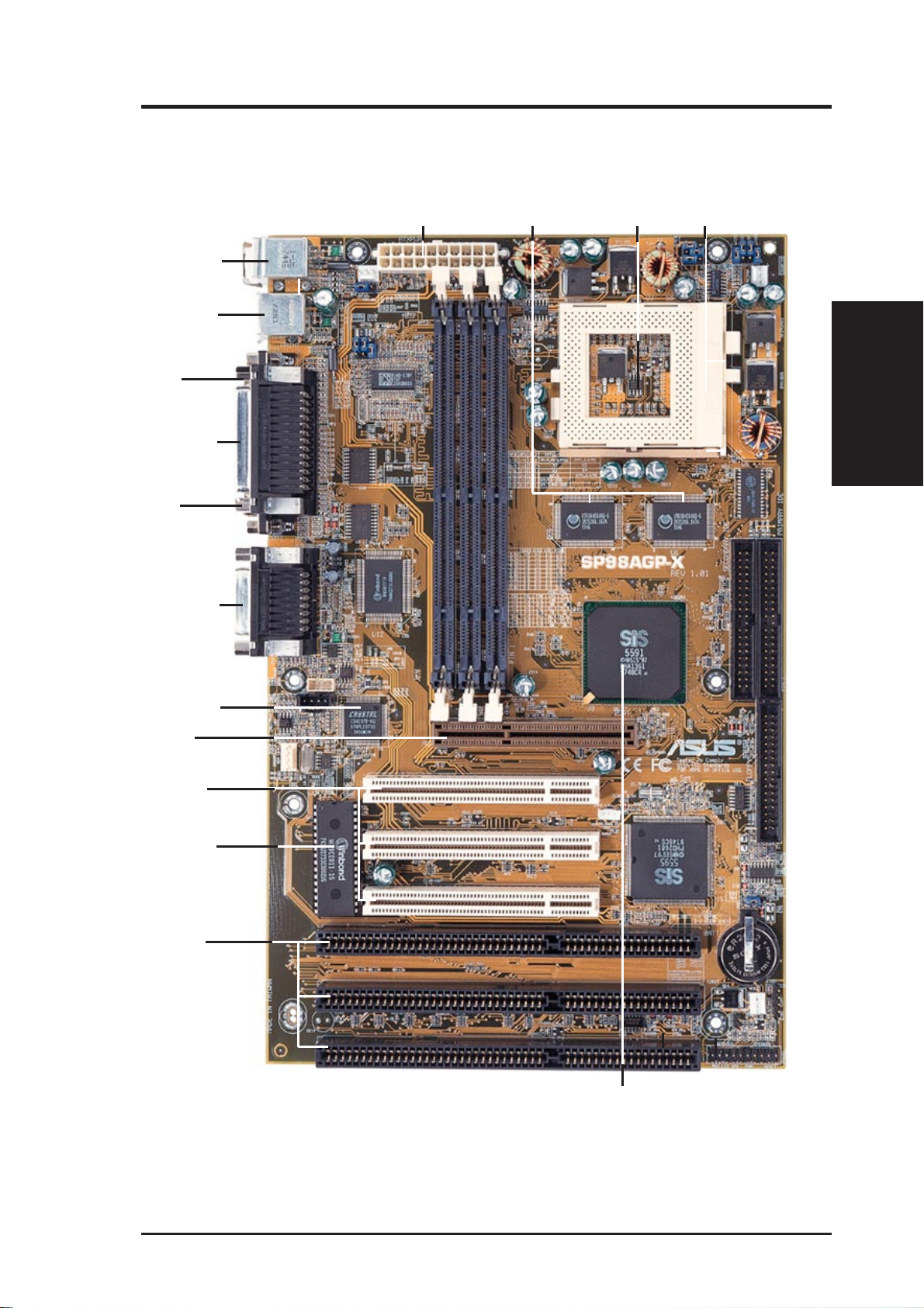
The ASUS SP98AGP-X Motherboard
T: PS/2 Mouse
B: PS/2 Keyboard
T: USB Port 1
B: USB Port 2
COM 1
T: Parallel Conn.
B: Serial Conn.
COM 2
(Optional)
T:Joystick/Midi
B:Out/In/Mic
ATX Power
Connector
512KB/1024KB Pipelined
Burst L2 Cache
CPU Thermal
Sensor
CPU ZIF
Socket 7
II. FEATURES
Motherboard Parts
(Optional)
Audio Chipset
AGP Port
3 PCI Slots
Programmable
Flash ROM
3 ISA Slots
SiS 5591
Chipset
ASUS SP98AGP-X User’s Manual 11
III. INSTALLATION
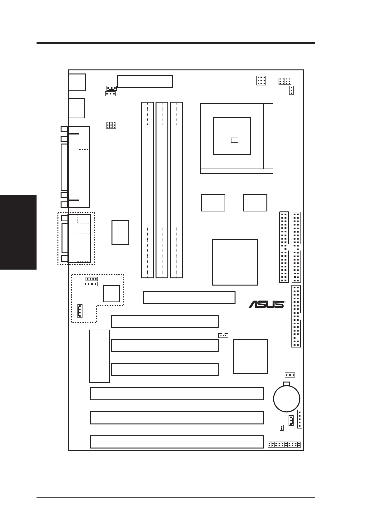
ASUS SP98AGP-X Motherboard Layout
PS/2
USB
Parallel Port
Motherboard Layout
III. INSTALLATION
Top: Mouse
Bottom: Keyboard
PWR_FAN
KBV_SEL
Top: USB 1
Bottom: USB 2
COM 1
COM 2
Line
Out
Line
In
Board Power Input
for ATX Power Supply
FS2
FS1
FS0
BUS FREQ
Multi-I/O
Chip
CPU ZIF Socket 7
CPU Thermal Sensor
(Hardware Monitor)
LM75
512KB/1024KB Onboard L2 Cache
DIMM Socket 1 (64-bit, 168-pin module)
DIMM Socket 2 (64-bit, 168-pin module)
DIMM Socket 3 (64-bit, 168-pin module)
BF2
BF1
BF0
BUS Freq.
VID3
VID2
VID1
VID0
CPU Voltage
CPU_FAN
Secondary IDE
Primary IDE
Game/Midi Port
Mic
In
CD 2
CD 1
Audio
Chipset
Modem
Connector
Programmable
BIOS EEPROM
Row
PCI Slot 1
PCI Slot 2
PCI Slot 3
ISA Slot 1
ISA Slot 2
ISA Slot 3
54
AGP Slot
32
10
SiS 5591
Chipset
Wake on LAN
SiS 5595
Chipset
with LM78
Hardware
Monitor
R
Floppy Drives
RTCLR
CR2032
3 Volt
Lithium Cell
CHA_FAN
IDE LED
Panel Connections
Infrared Con. (IrDA)
NOTE: Outlined items (thick dashes) are optional and may not be present.
12 ASUS SP98AGP-X User’s Manual

III. INSTALLATION
Jumpers
1) RTCLR p. 15 Real Time Clock RAM (Operation/Clear Data)
2) KBV_SEL p. 18 Keyboard Voltage Selection
3) FS0, FS1, FS2 p. 16 CPU External Clock (BUS) Frequency Selection
4) BF0, BF1, BF2 p. 16 CPU:BUS Frequency Ratio
5) VID0, 1, 2, 3 p. 18 CPU Voltage Regulator Output Selection
Expansion Slots
1) System Memory p. 19 System Memory Upgrade
2) CPU ZIF Socket 7 p. 22 Central Processing Unit (CPU) Socket
3) SLOT 1, 2, 3 p. 23 16-bit ISA Bus Expansion Slots
4) PCI 1, 2, 3 p. 23 32-bit PCI Bus Expansion Slots
Connectors
1) PS2KEYBOARD p. 25 PS/2 Keyboard Connector (6-pin Female)
2) PS2MOUSE p. 25 PS/2 Mouse Connector (6-pin Female)
3) PRINT p. 26 Parallel (Printer) Port Connector (25-pin Female)
4) COM1, COM2 p. 26 Serial Port COM1 & COM2 (T wo 9-pin Male)
5) FLOPPY p. 2 6 Floppy Drive Connector (34-pin Block)
6) AUDIO (optional) p. 27 Audio Port -Line Out, Line In, Mic (Three 1/8” Female)
7) GAME (optional) p. 27 Joystick/Midi Connector (15-pin Female)
8) USB p. 27 Universal Serial BUS Ports 1 & 2 (Two 4-pin Female)
9) Primary/Second. IDE p. 28 Primary / Secondary IDE Connector (40-pin Blocks)
10) IDELED p. 28 IDE LED Activity Light
11) CHA_/CPU_/PWR_FAN p. 29 Chassis, CPU, Power Supply Fan Power Lead (3-pin Block)
12) MDM (optional) p. 29 Modem connector (4 pins)
13) IR p. 30 Infrared Port Module Connector
14) ATXPWR p. 30 ATX Motherboard Power Connector (20-pin Block)
15) WOL p. 31 Wake on LAN (3 pins)
16) CD1 (optional) p. 31 Stereo audio in connector (4-pin Block)
17) CD2 (optional) p. 31 Stereo audio in connector (4-pin Block)
18) MSG.LED (PANEL) p. 32 System Message LED (2 pins)
19) SMI (PANEL) p. 32 SMI Switch Lead (2 pins)
20) PWR (PANEL) p. 32 ATX Power & Soft-Off Switch Lead (2 pins)
21) RESET (PANEL) p. 32 Reset Switch Lead (2 pins)
22)
KEYLOCK (
23)
KEYLOCK (
24) SPEAKER (PANEL) p. 32 Speaker Output Connector (4 pins)
PANEL)p. 32 System Power LED Lead ( 3 pins)
PANEL)p. 32 Keyboard Lock Switch Lead (2 pins)
*
III. INSTALLATION
*
The onboard hardware monitor uses the address 290H-297H so legacy ISA cards must not
use this address, otherwise conflicts will occur.
ASUS SP98AGP-X User’s Manual 13
III. INSTALLATION
III. INSTALLATION
Installation Steps
Before using your computer, you must complete the following steps:
1. Set Jumpers on the Motherboard
2. Install System Memory
3. Install the Central Processing Unit (CPU)
4. Install Expansion Cards
5. Connect Ribbon Cables, Cabinet Wires, and Power Supply
6. Setup the BIOS Software
1. Jumpers
Several hardware settings are made through the use of jumper caps to connect jumper
pins (JP) on the motherboard. See “Motherboard Layout” for locations of jumpers.
The jumper settings will be described numerically such as [----], [1-2], [2-3] for no
Jumpers
connection, connect pins 1&2, and connect pins 2&3 respectively . Pin 1 for our motherboards is always on top
the keyboard connector away from yourself. A “1” is written besides pin 1 on jumpers
with three pins. The jumpers will also be shown graphically such as to connect
pins 1&2 and to connect pins 2&3. Jumpers with two pins will be shown as
for Short (On) and for Open (Off). For manufacturing simplicity, the jumpers may be sharing pins from other groups. Use the diagrams in this manual instead of
following the pin layout on the board. Settings with two jumper numbers require that
both jumpers be moved together. To connect the pins, simply place a plastic jumper
cap over the two pins as diagramed.
WARNING! Computer motherboards, baseboards and components, such as SCSI
cards, contain very delicate Integrated Circuit (IC) chips. To protect them against
damage from static electricity , you should follow some precautions whenever you
work on your computer.
1. Unplug your computer when working on the inside.
PIN 1
or on the left
PIN 1
when holding the motherboard with
2. Use a grounded wrist strap before handling computer components. If you do
not have one, touch both of your hands to a safely grounded object or to a
metal object, such as the power supply case.
3. Hold components by the edges and try not to touch the IC chips, leads or
connectors, or other components.
4. Place components on a grounded antistatic pad or on the bag that came with
the component whenever the components are separated from the system.
14 ASUS SP98AGP-X User’s Manual
III. INSTALLATION
Jumper Settings
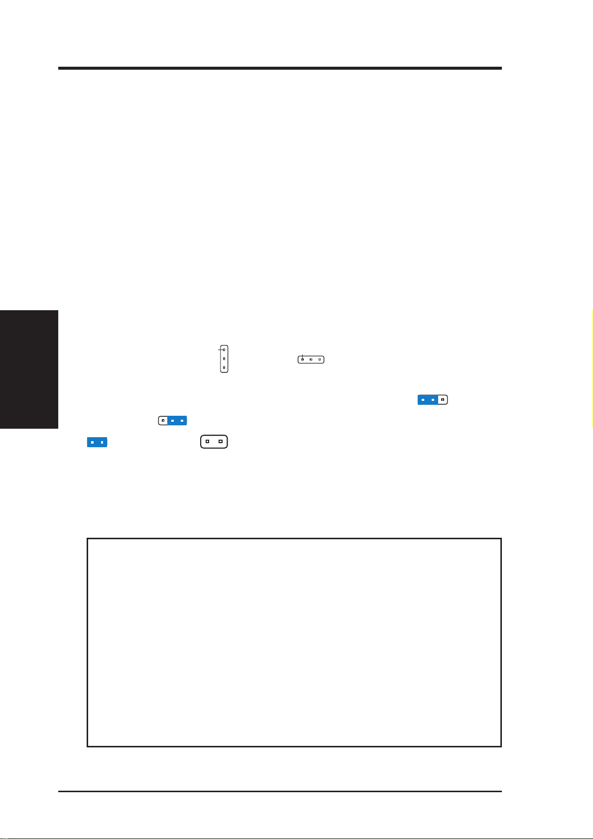
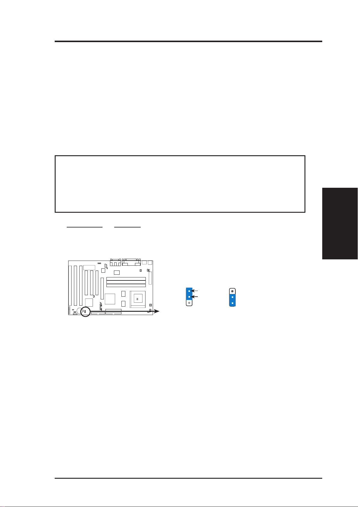
1. Real Time Clock (RTC) RAM (RTCLR)
The CMOS RAM is powered by the onboard button cell battery. To clear the
R TC data: (1) T urn of f your computer and remove the AC power , (2) Move this
jumper to “Clear CMOS,” (3) Move the jumper back to “Normal,” (4) T urn on
your computer, (5) Hold down <Delete> during bootup and enter BIOS setup to
re-enter user preferences.
Battery Test Jumper (RTCLR)
You can test the battery’s current by removing this jumper and attaching a current meter to pins 1&2.
WARNING! You must unplug the power cord to your power supply to ensure
that there is no power to your motherboard. The CMOS RAM containing BIOS
setup information may be cleared by this action. You must enter BIOS to “Load
Setup Defaults” and re-enter any user information after removing and reapplying this jumper.
RTC RAM RTCLR
Normal [1-2] (Default)
Clear CMOS [2-3] (momentarily)
RTCLR
R
RTC_VDD (Normal/Clear CMOS)
Normal (Default)
Jumpers
III. INSTALLATION
RTCLR
BATTERY TEST
Clear CMOS
ASUS SP98AGP-X User’s Manual 15
III. INSTALLATION
2. Keyboard Power Selection (KBV_SEL)
This jumper allows you to select the power current for your keyboard. Make
sure that your power supply can support at least 300mAmp +5VSB before selecting +5VSB.
Multi-I/O KBV_SEL
+5V [1-2] (Default)
+5VSB [2-3]
III. INSTALLATION
Jumpers
KBV_SEL
1
2
3
+5V (Default)
R
KBV_SEL
1
2
3
+5VSB
Keyboard Voltage Selection
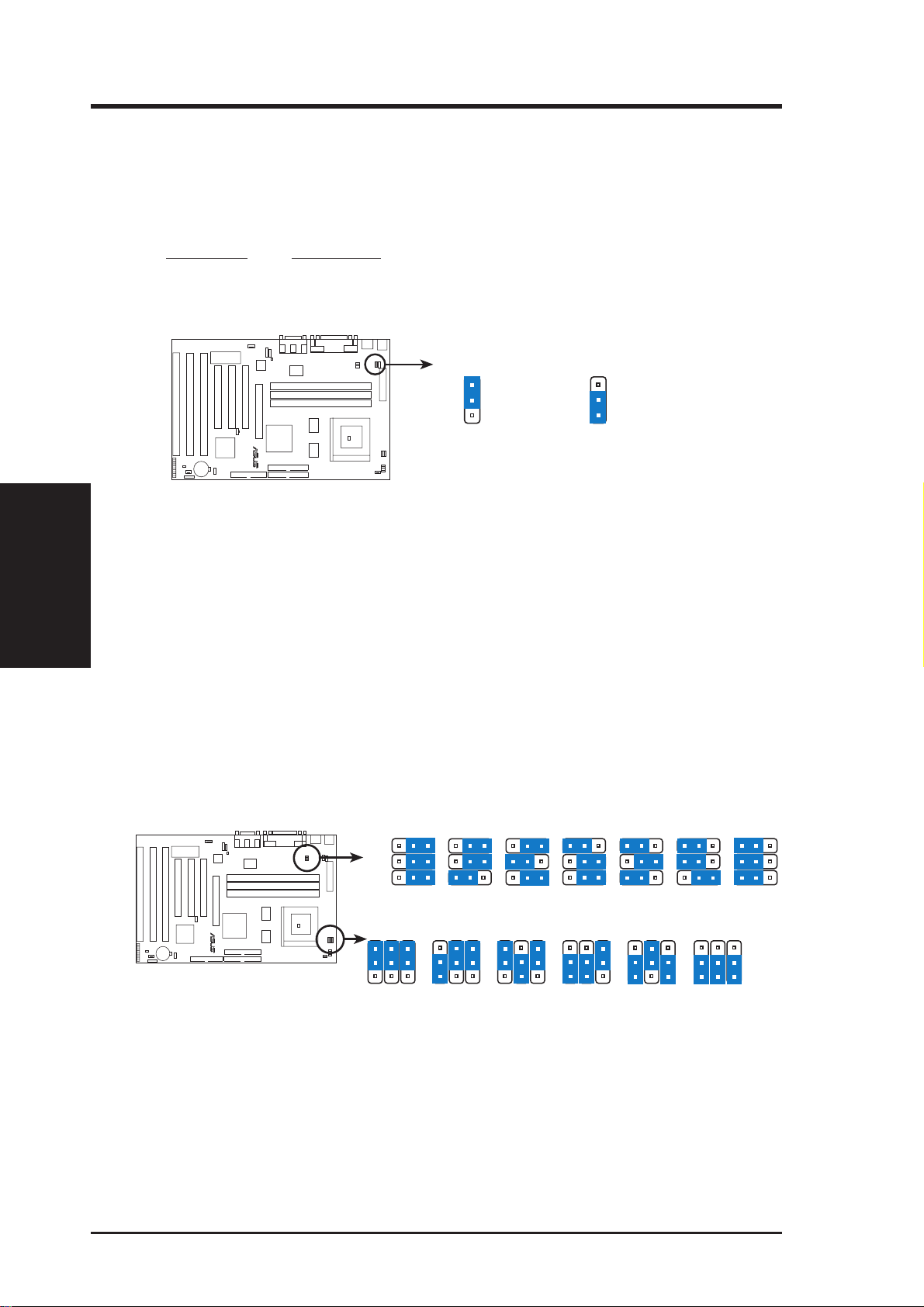
3. CPU External (BUS) Frequency Selection (FS0, FS1, FS2)
These jumpers tell the clock generator what frequency to send to the CPU. These
allow the selection of the CPU’ s External frequency (or BUS Clock). The BUS Clock
times the BUS Ratio equals the CPU’ s Internal frequency (the advertised CPU speed).
4. CPU to BUS Frequency Ratio (BF0, BF1, BF2)
These jumpers set the frequency ratio between the Internal frequency of the CPU
and the External frequency (called the BUS Clock) within the CPU. These must
be set together with the CPU External (BUS) Frequency Selection jumpers .
3
1
2
3
2
1
BF0
BF1
2.5x(5/2)
2.5x(5/2)
1.0x(1/1)
2.0x(2/1)
2.5x(5/2)
BF2
R
Match the “Ratio” column of
the table on the opposite page
to these CPU types:
CPU Types
CPU A →
CPU B →
CPU C →
CPU D →
CPU E →
3
2
1
FS2
FS1
FS0
60MHz 66.8MHz
CPU External Clock (BUS) Frequency Selection
BF0
BF2
BF1
1
2
3
1.5x(3/2)
3.5x(7/2)
3.0x(3/1)
3.0x(3/1)
3.5x(7/2)
CPU : BUS Frequency Ratio
2.0x(2/1)
2.0x(2/1)
2.0x(2/1)
2.0x(2/1)
2.0x(2/1)
BF0
3
2
1
BF1
BF2
1
2
3
2
1
68.5MHz 75MHz 83.3MHz
BF0
BF2
BF1
3.0x(3/1)
3.0x(3/1)
----
----
3.0x(3/1)
3
16 ASUS SP98AGP-X User’s Manual
1
2
3
3
2
1
BF0
BF1
----
----
----
----
4.0x(4/1)
3
2
1
90MHz 100MHz
BF2
1
2
3
4.5x(9/2)
BF0
----
----
----
----
BF1
1
BF2
1
2
3
3
2

III. INSTALLATION
Set the jumpers by the Internal speed of the Intel, AMD, IBM, or Cyrix CPU as follows:
(BUS Freq.) (Freq. Ratio)
CPU Model Freq. Ratio BUS Freq. FS2 FS1 FS0 BF0 BF1 BF2
Intel Pentium P54C 166MHz A-2.5x 66MHz [2-3] [2-3] [1-2] [2-3] [2-3] [1-2]
Intel Pentium P54C 150MHz A-2.5x 60MHz [2-3] [2-3] [2-3] [2-3] [2-3] [1-2]
Intel Pentium P54C 133MHz A-2.0x 66MHz [2-3] [2-3] [1-2] [2-3] [1-2] [1-2]
Intel Pentium P54C 120MHz A-2.0x 60MHz [2-3] [2-3] [2-3] [2-3] [1-2] [1-2]
Intel Pentium P54C 100MHz A-1.5x 66MHz [2-3] [2-3] [1-2] [1-2] [1-2] [1-2]
Intel Pentium P54C 90MHz A-1.5x 60MHz [2-3] [2-3] [2-3] [1-2] [1-2] [1-2]
AMD-K5-PR13 100MHz A-1.5x 66MHz [2-3] [2-3] [1-2] [1-2] [1-2] [1-2]
AMD-K5-PR120 90MHz A-1.5x 60MHz [2-3] [2-3] [2-3] [1-2] [1-2] [1-2]
AMD-K5-PR100 100MHz A-1.5x 66MHz [2-3] [2-3] [1-2] [1-2] [1-2] [1-2]
AMD-K5-PR90 90MHz A-1.5x 60MHz [2-3] [2-3] [2-3] [1-2] [1-2] [1-2]
Intel Pentium P55C 233MHz B-3.5x 66MHz [2-3] [2-3] [1-2] [1-2] [1-2] [1-2]
Intel Pentium P55C 200MHz B-3.0x 66MHz [2-3] [2-3] [1-2] [1-2] [2-3] [1-2]
Intel Pentium P55C 166MHz B-2.5x 66MHz [2-3] [2-3] [1-2] [2-3] [2-3] [1-2]
IBM/Cyrix 6x86MX-PR233 200MHz B-3.0x 66MHz [2-3] [2-3] [1-2] [1-2] [2-3] [1-2]
IBM/Cyrix 6x86MX-PR233 166MHz B-2.0x 83MHz [1-2] [2-3] [1-2] [2-3] [1-2] [1-2]
IBM/Cyrix 6x86MX-PR200 166MHz B-2.5x 66MHz [2-3] [2-3] [1-2] [2-3] [2-3] [1-2]
IBM/Cyrix 6x86MX-PR200 150MHz B-2.0x 75MHz [1-2] [2-3] [2-3] [2-3] [1-2] [1-2]
IBM/Cyrix 6x86MX-PR166 150MHz B-2.5x 60MHz [2-3] [2-3] [2-3] [2-3] [2-3] [1-2]
*IBM/Cyrix 6x86-PR166+ 133MHz C-2.0x 66MHz [2-3] [2-3] [1-2] [2-3] [1-2] [1-2]
*IBM/Cyrix 6x86L-PR166+ 133MHz D-2.0x 66MHz [2-3] [2-3] [1-2] [2-3] [1-2] [1-2]
AMD-K6-PR300 300MHz E-4.5x 66MHz [2-3] [2-3] [1-2] [2-3] [2-3] [2-3]
AMD-K6-PR266 266MHz E-4.0x 66MHz [2-3] [2-3] [1-2] [2-3] [1-2] [2-3]
AMD-K6-PR233 233MHz E-3.5x 66MHz [2-3] [2-3] [1-2] [1-2] [1-2] [1-2]
AMD-K6-PR200 200MHz E-3.0x 66MHz [2-3] [2-3] [1-2] [1-2] [2-3] [1-2]
AMD-K6-PR166 166MHz E-2.5x 66MHz [2-3] [2-3] [1-2] [2-3] [2-3] [1-2]
Jumpers
III. INSTALLATION
*NOTE: The only IBM or Cyrix 6x86(L or M1) that is supported on this motherboard is Rev 2.7 or later. Look on the
underside of the CPU for the serial number . The number should
read G8DC6620A or later.
ASUS SP98AGP-X User’s Manual 17
III. INSTALLATION
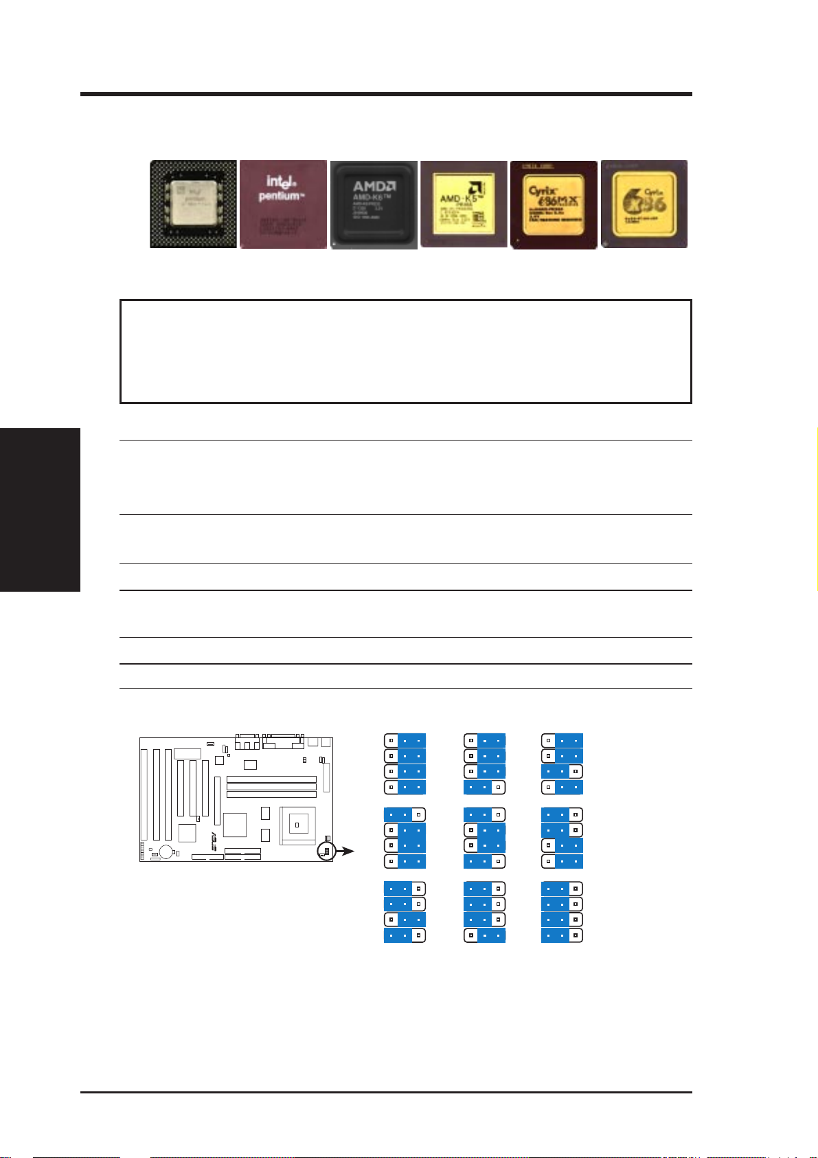
5. Voltage Regulator Output Selection (VID0, 1, 2, 3)
These jumpers set the voltage supplied to the CPU.
III. INSTALLATION
Jumpers
Pentium MMX (P55C)
(150MHz-233MHz)
Intel Pentium (P54C)
(75MHz-200MHz)
AMD-K6
(PR166 and faster)
AMD-K5
(PR75-PR133)
IBM/Cyrix 6x86(MX)
(PR166 and faster)
IBM/Cyrix 6x86(M1)
(PR166 and faster)
WARNING! Because CPU designs change rapidly, the following chart is only
intended as a simple quideline and is not intended to be true for your CPU. Look
for the CPU voltage included with your CPU and follow the Voltage setting
diagramed below the chart.
Manufacturer CPU Type Single Plane Dual Plane VID3 VID2 VID1 VID0
Intel P54C/P54CS 3.5V(VRE) ---- [1-2] [1-2] [1-2] [1-2]
AMD K5 3.5V(VRE) ---- [1-2] [1-2] [1-2] [1-2]
IBM/Cyrix 6x86 3.5V(VRE) ---- [1-2] [1-2] [1-2] [1-2]
Intel P54C/P54CS 3.4V(STD) ---- [1-2] [1-2] [1-2] [2-3]
AMD K5 3.4V(STD) ---- [1-2] [1-2] [1-2] [2-3]
AMD(.35 micron) K6-PR233 ---- 3.2V(Dual) [1-2] [1-2] [2-3] [2-3]
AMD(.35 micron) K6-166,200 ---- 2.9V(Dual) [1-2] [2-3] [2-3] [1-2]
IBM/Cyrix 6x86MX ---- 2.9V(Dual) [1-2] [2-3] [2-3] [1-2]
Intel P55C-MMX ---- 2.8V(Dual) [1-2] [2-3] [2-3] [2-3]
AMD (.25micron) K6-233,266,300 ---- 2.2V(Dual) [2-3] [2-3] [1-2] [2-3]
R
Voltage Regulator Output Selection
123
VID3
VID2
VID1
VID0
VID3
VID2
VID1
VID0
2.8 Volts
VID3
VID2
VID1
VID0
3.3 Volts
VID3
VID2
VID1
VID0
VID3
VID2
VID1
VID0
VID3
VID2
VID1
VID0
123
2.9 Volts
3.4 Volts
123
VID3
VID2
VID1
VID0
2.2 Volts2.0 Volts 2.1 Volts
VID3
VID2
VID1
VID0
3.2 Volts
VID3
VID2
VID1
VID0
3.5 Volts
18 ASUS SP98AGP-X User’s Manual
III. INSTALLATION
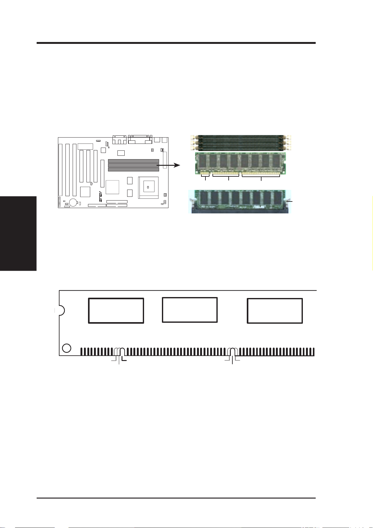
2. System Memory (DIMM)
Only Dual Inline Memory Modules (DIMMs) can be used with this motherboard.
Three sockets are available for 3.3Volt (power level) Unbuffered Synchronous
DRAMs (SDRAMs; 8, 16, 32, 64, or 128MB) or EDO DRAM (8, 16, 32, 64, 128, or
256MB) to form a memory size between 8MB to 768MB. One side (with memory
chips) of the DIMM module takes up one Row on the motherboard. If ECC-supported DIMM is used, you can enable the ECC function through BIOS setup –
CHIPSET FEATURES SETUP “Data Integrity Mode.”
IMPORTANT: You must first set the memory speed through the “EDO/FPM Con-
figuration” under the BIOS Chipset Setup of the BIOS SOFTWARE.
Install memory in any combination as follows:
DIMM Type 168-pin DIMM Memory Modules Total Memory
Socket 1 SDRAM 8, 16, 32, 64, 128MB x1
(Rows 0&1) EDO 8, 16, 32, 64, 128, 256MB
Socket 2 SDRAM 8, 16, 32, 64, 128MB x1
(Rows 2&3) EDO 8, 16, 32, 64, 128, 256MB
Socket 3 SDRAM 8, 16, 32, 64, 128MB x1
(Rows 4&5) EDO 8, 16, 32, 64, 128, 256MB
Total System Memory (Max 768MB) =
WARNING: Memory modules must have 18 chips or less. Memory modules with
more that 18 chips will cause unstable operation.
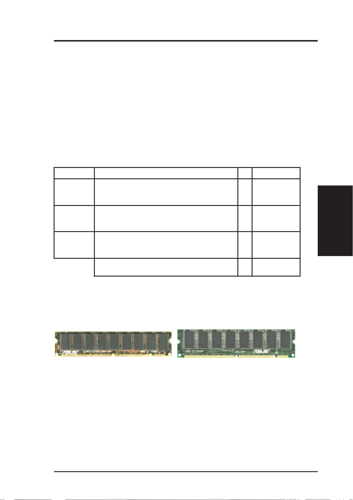
ASUS DIMM Module Examples:
ECC EDO DIMM (9 chips) Non-ECC SDRAM DIMM (8 chips)
System Memory
III. INSTALLATION
General DIMM Notes: (not true for all memory modules)
• Four possible memory chips are supported: EDO or SDRAM with and without parity.
• SDRAM chips are generally thinner with higher pin density than EDO chips.
• BIOS shows EDO or SDRAM memory on bootup screen.
• 8 chip/side modules do not support parity, only 9 chip/side modules support parity.
• Single sided modules are usually 16 or 64 MB, double sided are usually 8, 32, or 128MB.
ASUS SP98AGP-X User’s Manual 19
III. INSTALLATION
DIMM Memory Installation Procedures:
Insert the module(s) as shown. Because the number of pins are different on either
side of the breaks, the module will only fit in the orientation as shown. DRAM
SIMM modules have the same pin contact on both sides. SDRAM DIMM modules
have different pin contact on each side and therefore have a higher pin density.
88 Pins60 Pins20 Pins
III. INSTALLATION
System Memory
168 Pin DIMM Memory Sockets
The Dual Inline Memory Module (DIMM) memory modules must be 3.3Volt Unbuffered Synchronous DRAM (SDRAM) or Extended Data Output (EDO) . You
can identify the type of DIMM module by the illustration below:
168-Pin DIMM Notch Key Definitions (3.3V)
R
DRAM Key Position
RFU
Buffered
Unbuffered
Voltage Key Position
5.0V
Reserved
3.3V
Lock
The notch on the DIMM module will shift between left, center, or right to identify
the type and also to prevent the wrong type to be inserted into the DIMM slot on the
motherboard. You must ask your retailer for the specifications before purchasing.
Four clock signals are supported on this motherboard.
20 ASUS SP98AGP-X User’s Manual
 Loading...