

Page 1
Page 2

Version 1.0
Published March 2020
Copyright©2020 ASRock INC. All rights reserved.
Copyright Notice:
No part of this documentation may be reproduced, transcribed, transmitted, or
translated in any language, in any form or by any means, except duplication of
documentation by the purchaser for backup purpose, without written consent of
ASRock Inc.
Products and corporate names appearing in this documentation may or may not
be registered trademarks or copyrights of their respective companies, and are used
only for identication or explanation and to the owners’ benet, without intent to
infringe.
Disclaimer:
Specications and information contained in this documentation are furnished for
informational use only and subject to change without notice, and should not be
constructed as a commitment by ASRock. ASRock assumes no responsibility for
any errors or omissions that may appear in this documentation.
With respect to the contents of this documentation, ASRock does not provide
warranty of any kind, either expressed or implied, including but not limited to
the implied warranties or conditions of merchantability or tness for a particular
purpose.
In no event shall ASRock, its directors, ocers, employees, or agents be liable for
any indirect, special, incidental, or consequential damages (including damages for
loss of prots, loss of business, loss of data, interruption of business and the like),
even if ASRock has been advised of the possibility of such damages arising from any
defect or error in the documentation or product.
is device complies with Part 15 of the FCC Rules. Operation is subject to the following
two conditions:
(1) this device may not cause harmful interference, and
(2) this device must accept any interference received, including interference that
may cause undesired operation.
CALIFORNIA, USA ONLY
e Lithium battery adopted on this motherboard contains Perchlorate, a toxic substance
controlled in Perchlorate Best Management Practices (BMP) regulations passed by the
California Legislature. When you discard the Lithium battery in California, USA, please
follow the related regulations in advance.
“Perchlorate Material-special handling may apply, see ww w.dtsc.ca.gov/hazardouswaste/
perchlorate”
ASRock Website: http://www.asrock.com
Page 3

AUSTRALIA ONLY
Our goods come with guarantees that cannot be excluded under the Australian
Consumer Law. You are entitled to a replacement or refund for a major failure and
compensation for any other reasonably foreseeable loss or damage caused by our
goods. You are also entitled to have the goods repaired or replaced if the goods fail
to be of acceptable quality and the failure does not amount to a major failure. If
you require assistance please call ASRock Tel : +886-2-28965588 ext.123 (Standard
International call charges apply)
e terms HDMI® and HDMI High-Denition Multimedia Interface, and the
HDMI logo are trademarks or registered trademarks of HDMI Licensing LLC in the
United States and other countries.
Page 4
CE Warning
is device complies with directive 2014/53/EU issued by the Commision of the European
Community.
is equipment complies with EU radiation exposure limits set forth for an uncontrolled
environment.
is equipment should be installed and operated with minimum distance 20cm between
the radiator & your body.
Operations in the 5.15-5.35GHz band are restricted to indoor usage only.
Radio transmit power per transceiver ty pe
Function Frequency Maximum Output Power (EIRP)
2400-2483.5 MHz 18.5 + / -1.5 dbm
5150-5250 MHz 21.5 + / -1.5 dbm
WiFi
Bluetooth 2400-2483.5 MHz 8.5 + / -1.5 dbm
5250-5350 MHz
5470-5725 MHz
18.5 + / -1.5 dbm (no TPC)
21.5 + / -1.5 dbm (TPC)
25.5 + / -1.5 dbm (no TPC)
28.5 + / -1.5 dbm (TPC)
Page 5

Contents
Chapter 1 Introduction 1
1.1 Package Contents 1
1.2 Specications 2
1.3 Motherboard Layout 9
1.4 I/O Panel 11
Chapter 2 Installation 14
2.1 Installing the CPU 15
2.2 Installing the CPU Fan and Heatsink 18
2.3 Installing Memory Modules (DIMM) 19
2.4 Expansion Slots (PCI Express Slots) 21
2.5 MOS Heatsink Height 22
2.6 Jumpers Setup 23
2.7 Onboard Headers and Connectors 24
2.8 Smart Switches 30
2.9 Dr. Debug 32
2.10 SLITM Operation Guide 38
2.11 CrossFireXTM , 3-Way CrossFireXTM and Quad CrossFireXTM
Operation Guide 41
2.11.2 Installing Three CrossFireXTM-Ready Graphics Cards 43
2.12 M.2_SSD (NGFF) Module Installation Guide
(M 2 _1) 45
2.13 M.2_SSD (NGFF) Module Installation Guide (M2_2) 48
Page 6

2.14 M.2_SSD (NGFF) Module Installation Guide (M2_3) 52
Chapter 3 Software and Utilities Operation 56
3.1 Installing Drivers 56
3.2 ASRock Motherboard Utility (A-Tuning) 57
3.2.1 Installing ASRock Motherboard Utility (A-Tuning) 57
3.2.2 Using ASRock Motherboard Utility (A-Tuning) 57
3.3 ASRock Live Update & APP Shop 60
3.3.1 UI Overview 60
3.3.2 Apps 61
3.3.3 BIOS & Drivers 64
3.3.4 Setting 65
3.4 Nahimic Audio 66
3.5 ASRock Polychrome SYNC 67
Chapter 4 UEFI SETUP UTILITY 70
4.1 Introduction 70
4.2 EZ Mode 71
4.3 Advanced Mode 72
4.3.1 UEFI Menu Bar 72
4.3.2 Navigation Keys 73
4.4 Main Screen 74
4.5 OC Tweaker Screen 75
4.6 Advanced Screen 87
4.6.1 CPU Conguration 88
4.6.2 Chipset Conguration 90
Page 7

4.6.3 Storage Conguration 93
4.6.4 Intel(R) Thunderbolt 95
4.6.5 Super IO Conguration 96
4.6.6 ACPI Conguration 97
4.6.7 USB Conguration 98
4.6.8 Trusted Computing 99
4.7 Tools 100
4.8 Hardware Health Event Monitoring Screen 102
4.9 Security Screen 107
4.10 Boot Screen 108
4.11 Exit Screen 111
Page 8

Chapter 1 Introduction
ank you for purchasing ASRock Z 490 Taichi motherboard, a reliable
motherboard produced under ASRock’s consistently stringent quality control.
It delivers excellent performance with robust design conforming to ASRock’s
commitment to quality and endurance.
In this documentation, Chapter 1 and 2 contains the introduction of the
motherboard and step-by-step installation guides. Chapter 3 contains the operation
guide of the soware and utilities. Chapter 4 contains the conguration guide of
the BIOS setup.
Becau se the motherboard specications and the BIOS soware might be updated, the
content of this documentation will be subject to change without notice. In case any modications of this documentation occur, the updated version will be available on ASRock’s
website w ithout further notice. If you require technical support related to this motherboard, please visit our website for specic information about the model you are using. You
may nd the l atest VGA cards and CPU suppor t list on ASRock’s website a s well. ASRock
website http://www.asrock.com.
Z490 Taichi
1.1 Package Contents
ASRock Z490 Taichi Motherboard (ATX Form Factor)
•
ASRock Z490 Taichi Quick Installation Guide
•
ASRock Z490 Taichi Support CD
•
4 x Serial ATA (SATA) Data Cables (Optional)
•
1 x ASRock SLI_HB_Bridge_2S Card
•
1 x ASRock WiFi 2.4/5 GHz Antenna
•
1 x ASRock Screwdriver (Optional)
•
3 x Screws for M.2 Sockets (Option al)
•
2 x Standos for M.2 Sockets (Opt iona l)
•
English
1
Page 9

1.2 Specications
Platform
CPU
Chipset
Memory
•
•
•
•
•
•
•
•
•
•
•
•
•
* Please refer to Memory Support List on ASRock's website for
more information. (http://www.asrock.com/)
* CoreTM (i9/i7) support DDR4 up to 2933; CoreTM (i5/i3),
Pentium® and Celeron® support DDR4 up to 2666.
•
•
•
•
ATX Form Factor
2oz Copper PCB
Suppor ts 10th Gen and future generation Intel® CoreTM
Processors (Socket 1200)
Digi Power design
14 Power Phase design
Supports Intel® Turbo Boost Ma x 3.0 Technology
Supports Intel® K-Series unlocked CPUs
Supports ASRock BCLK Full-range Overclocking
Supports ASRock Hyper BCLK Engine III
Intel® Z490
Dual Channel DDR4 Memory Technology
4 x DDR4 DIMM Slots
Support s DDR4 4666 +(OC)*/4 600/4500/4400/4333/4 266
(OC)/4133(OC)/4000(OC)/3866(OC)/3800(OC)/3733(OC)/
3600(OC)/3200(OC)/2933/2800/2666/2400/2133 non-ECC,
un-buered memory
Supports ECC UDIMM memory modules (operate in non-
ECC mode)
Max. capacity of system memory: 128GB
Supports Intel® Extreme Memory Prole (XMP) 2.0
15μ Gold Contact in DIMM Slots
English
2
Expansion
Slot
3 x PCI Express 3.0 x16 Slots (PCIE1/PCIE3/PCIE5: single at
•
x16 (PCIE1); dual at x16 (PCIE1) / x8 (PCIE3); triple at x16
(PCIE1) / x8 (PCIE3) / x4 (PCIE5))*
* Supports NVMe SSD as boot disks
2 x PCI Express 3.0 x1 Slots
•
Page 10

Graphics
Supports AMD Quad CrossFireXTM, 3-Way CrossFireXTM
•
and CrossFireXTM
Supports NVIDIA® SLI
•
Support NVIDIA® SLITM with NVIDIA® Quadro graphics
•
cards
Supports NVIDIA® NVLinkTM with dual NVIDIA® GeForce®
•
RTX series graphics cards**
** NVIDIA NVLink Bridge does not come with the package.
Please purchase it from NVIDIA® if necessary.
1 x Vertical M.2 Socket (Key E) with the bundled WiFi-
•
802.11ax module (on the rear I/O)
15μ Gold Contact in VGA PCIe Slot (PCIE1)
•
Intel® UHD Graphics Built-in Visuals and the VGA outputs
•
can be supported only with processors which are GPU
integrated.
Hardware Accelerated Codecs: AVC/H.264, HEVC/H.265
•
8bit, HEVC/H.265 10bit, VP8, VP9 8bit, VP9 10bit, MPEG 2,
MJ PEG, VC-1
* VP9 10bit and VC-1 are for decode only.
* VP8 and VP9 encode are not supported by Windows OS.
Graphics, Media & Compute: Microso DirectX 12, OpenGL
•
4.5, Intel® Built In Visuals, Intel® Quick Sync Video, Hybrid /
Switchable Graphics, OpenCL 2.1
Display & Content Security: Rec. 2020 (Wide Color Gamut),
•
Microso PlayReady 3.0, Intel® SGX Content Protection,
UHD/HDR Blu-ray Disc
Dual graphics output: support HDMI and DisplayPort 1.4
•
ports by independent display controllers
Supports HDMI 1.4 with max. resolution up to 4K x 2K
•
(4096x2160) @ 30Hz
Supports DisplayPort 1.4 with max. resolution up to 4K x 2K
•
(4096x2304) @ 60Hz
Supports Auto Lip Sync, Deep Color (12bpc), xvYCC and
•
HBR (High Bit Rate Audio) with HDMI 1.4 Port (Compliant
HDMI monitor is required)
Supports HDCP 2.3 with HDMI 1.4 and DisplayPort 1.4
•
Ports
Supports 4K Ultra HD (UHD) playback with HDMI 1.4 and
•
DisplayPort 1.4 Ports
TM
Z490 Taichi
English
3
Page 11

Audio
7.1 CH HD Audio with Content Protection (Realtek
•
ALC1220 Audio Codec)
Premium Blu-ray Audio support
•
Supports Surge Protection
•
WIMA Audio Capacitors (For Front Outputs)
•
ESS SABR E9218 DAC for Front Panel Audio
•
120dB SNR DAC with Dierential Amplier
•
Pure Power-In
•
Direct Drive Technology
•
PCB Isolate Shielding
•
Impedance Sensing on Rear Out port
•
Individual PCB Layers for R/L Audio Channel
•
Gold Audio Jacks
•
15μ Gold Audio Connector
•
Nahimic Audio
•
English
LAN
1 x 2.5 Gigabit LAN 10/100/1000/2500 Mb/s (Dragon RTL-
8125BG)
Supports Dragon 2.5G LAN Soware
•
- Smart Auto Adjust Bandwidth Control
- Visual User Friendly UI
- Visual Network Usage Statistics
- Optimized Default Setting for Game, Browser, and
Streaming Modes
- User Customized Priority Control
Supports Wake-On-LAN
•
Supports Lightning/ESD Protection
•
Supports Energy Ecient Ethernet 802.3az
•
Supports PXE
•
1 x Gigabit LAN 10/100/1000 Mb/s (Intel® I219V)
Supports Wake-On-LAN
•
Supports Lightning/ESD Protection
•
Supports Energy Ecient Ethernet 802.3az
•
Supports PXE
•
4
Page 12

Wireless
LAN
Rear Panel
I/O
Intel® 802.11ax WiFi Module
•
Supports IEEE 802.11a/b/g/n/ax
•
Supports Dual-Band (2.4/5 GHz)
•
Supports WiFi6 802.11ax (2.4Gbps)
•
2 antennas to support 2 (Transmit) x 2 (Receive) diversity
•
technolog y
Supports Bluetooth 5.1 + High speed class II
•
Supports MU-MIMO
•
2 x Antenna Ports
•
1 x PS/2 Mouse/Keyboard Port
•
1 x HDMI Port
•
1 x DisplayPort 1.4
•
1 x Optical SPDIF Out Port
•
2 x USB 3.2 Gen2 Type-A Ports (10 Gb/s) (ReDriver)
•
(Supports ESD Protection)
1 x USB 3.2 Gen2x2 Type-C Port (20 Gb/s) (ASMedia
•
ASM3242) (Supports ESD Protection)
* M2_ 3, SATA3_4, SATA3_5 and USB32_TC_1 share lanes. If
either one of them is in use, USB32_TC_1 will downgrade to 16
Gb/s ma x.
5 x USB 3.2 Gen1 Ports (Supports ESD Protection)
•
* USB3_3 is from Intel® Z490; USB3_12 and USB3_4 _5 are from
ASMedia ASM1074 hub.
* Ultra USB Power is supported on USB3_4_5 ports.
* ACPI wake-up function is not supported on USB3_4_5 ports.
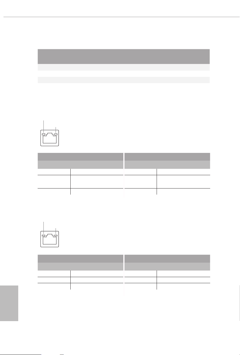
2 x RJ-45 LAN Ports with LED (ACT/LINK LED and SPEED
•
LED)
1 x BIOS Flashback Button
•
HD Audio Jacks: Rear Speaker / Centra l / Bass / Line in /
•
Front Speaker / Microphone (Gold Audio Jacks)
Z490 Taichi
Storage
6 x SATA3 6.0 Gb/s Connectors, support RAID (RAID 0,
•
RAID 1, RAID 5, RAID 10, Intel Rapid Storage Technology
17), NCQ, AHCI and Hot Plug*
2 x SATA3 6.0 Gb/s Connectors by ASMedia ASM1061,
•
support NCQ, AHCI and Hot Plug
* M2_ 2, SATA3_0 and SATA3_1 share lanes. If either one of
them is in use, the others will be disabled.
* M2_ 3, SATA3_4 and SATA3_5 share lanes. If either one of
them is in use, the others will be disabled.
English
5
Page 13

English
Connector
* M2_ 3, SATA3_4, SATA3_5 and USB32_TC_1 share lanes. If
either one of them is in use, USB32_TC_1 will downgrade to 16
Gb/s ma x.
1 x Ultra M.2 Socket (M2_1), supports M Key type 2280 M.2
•
PCI Express module up to Gen3 x4 (32 Gb/s)**
1 x Ultra M.2 Socket (M2_2), supports M Key ty pe
•
2260/2280 M.2 SATA3 6.0 Gb/s module and M.2 PCI
Express module up to Gen3 x4 (32 Gb/s)**
1 x Ultra M.2 Socket (M2_3), supports M Key ty pe
•
2230/2242/2260/2280/22110 M.2 SATA3 6.0 Gb/s module
and M.2 PCI Express module up to Gen3 x4 (32 Gb/s)**
** Supports Intel® OptaneTM Technology (M2 _1 and M2_2 only)
** Supports NVMe SSD as boot disks
** Supports ASRock U.2 Kit
1 x SPI TPM Header
•
1 x Power LED and Speaker Header
•
2 x RGB LED Headers
•
* Support in total up to 12V/3A, 36W LED Strip
2 x Addressable LED Headers
•
* Support in total up to 5V/3A, 15W LED Strip
1 x CPU Fan Connector (4-pin)
•
* e CPU Fan Connector supports the CPU fan of ma ximum
1A (12W) fan power.
1 x CPU/Water Pump Fan Connector (4-pin) (Smart Fan
•
Speed Control)
6 x Chassis/Water Pump Fan Connectors (4-pin) (Smart Fan
•
Speed Control)
* e Chassis/Water Pump Fan supports the water cooler fan of
maximum 2A (24W) fan power.
* CPU_FAN2/WP_3A, CHA_FAN1/WP, CHA_FAN2/WP,
CHA_FAN3/WP, CHA_FAN4/WP, CHA_FAN5/WP and
CHA_FAN6/WP can auto detect if 3-pin or 4-pin fan is in use.
* CPU_FAN2/WP_3A supports the water cooler fan of
maximum 3A (36W) fan power.
6
Page 14

BIOS
Feature
1 x 24 pin ATX Power Connector (Hi-Density Power
•
Connec tor)
2 x 8 pin 12V Power Connectors (Hi-Density Power
•
Connec tor)
1 x Front Panel Audio Connector (15μ Gold Audio
•
Connec tor)
1 x underbolt AIC Connector (5-pin) (Supports ASRock
•
underbolt 3 AIC R2.0 Card only)
2 x USB 2.0 Headers (Support 4 USB 2.0 ports) (Intel® Z490)
•
(Supports ESD Protection)
2 x USB 3.2 Gen1 Headers (Support 4 USB 3.2 Gen1 ports)
•
(ASMedia ASM1074 hub) (Supports ESD Protection)
1 x Front Panel Type C USB 3.2 Gen2 Header (Intel® Z490)
•
(Supports ESD Protection)
1 x Clear CMOS Button
•
1 x Dr. Debug with LED
•
1 x Power Button with LED
•
1 x Reset Button with LED
•
AMI UEFI Legal BIOS with multilingual GUI support
•
ACPI 6.0 Compliant wake up events
•
SMBIOS 2.7 Support
•
CPU Core/Cache, CPU GT, DRAM, VPPM, VCCSFR,
•
VCCPLL, VCCSTG, VCCSTG_OUT, PCH Voltage, VCCIO,
VCCST, VCCSA, CPU Internal PLL, GT PLL, Ring PLL,
System Agent PLL , Memory Controller PLL Voltage Multi-
adjustment
Z490 Taichi
Hardware
Monitor
Temperature Sensing: CPU, CPU/Water Pump, Chassis/
•
Water Pump Fans
Fan Tachometer: CPU, CPU/Water Pump, Chassis/Water
•
Pump Fans
Quiet Fan (Auto adjust chassis fan speed by CPU
•
temperature): CPU, CPU/Water Pump, Chassis/Water Pump
Fans
Fan Multi-Speed Control: CPU, CPU/Water Pump, Chassis/
•
Water Pump Fans
Voltage monitoring: +12V, +5V, +3.3V, CPU Vcore, DRAM,
•
VPPM, PCH, VCCSA, VCCST, VCCIO, VCCFSR_OC,
VCCSFR
English
7
Page 15
Microso® Windows® 10 64-bit
OS
Certications
* For detailed product information, please visit our website: http://www.asrock .com
Please realiz e that the re is a certain r isk involved with o verclocking, including adjusting
the setting in the BIOS, applying Untied Overclocking Technolog y, or using third-party
overclocking to ols. O verclocking may aect your system’s stability, or even c ause damage to
the components and devices of your system. It should be don e at your ow n risk and expense.
We are not responsibl e for possible damage caused by overclo cking.
•
FCC, CE
•
ErP/EuP ready (ErP/EuP ready power supply is required)
•
English
8
Page 16

Intel
Z490
DD R4_A2 ( 64 bit, 2 88-pi n modul e)
DD R4_A1 ( 64 bit, 2 88-pi n modul e)
DD R4_B2 ( 64 bit, 2 88-pi n modul e)
DD R4_B1 ( 64 bit, 2 88-pi n modul e)
ATX12V1
ATX PWR 1
LAN
PCIE1
PCIE3
HDLEDRESET
PLEDPWRBTN
1
SPK_PLED1
1
HD_AUDIO1
SATA3_2 _3
SATA3_4 _5
SATA3_A 1_A2
RoHS
8
9
11
14
15
16
17
USB_1_21USB_3_4
1
25
SATA3_0 _1
1
6
5
PCIE2
M2_ 4
CT11
CT24
CT34
CT35
CT32 CT31
CT23
CT33
1
USB3_ 8_9
1
21
CPU_FAN1
28
PCIE4
CT42
CHA_FAN1/WP
CPU_FAN2/WP_3A
CHA_FAN5/WP
3
33
LAN
30
2
ADDR_LED2
1
34
35
AUDIO
CODEC
Dr.
Debug
ATX12V2
RGB_LED2
1
7
CHA_FAN6
/WP
1
USB3_ 6_7
10
PANEL1
Reset
Power
22
24
1
SPI_TPM_J1
CLRMOS1
1
RGB_LED1
1
ADDR_LED1
1
T B1
M2_3
M2_ 1
HD MI1
DI SPL AY1
20
PCIE5
4
CHA_FAN3
/WP
18
19
2729
CHA_FAN4/WP
31
USB31_TC_2
12
13
BIOS
ROM
Z49 O Taich i
CMOS
Battery
M2_2
USB 3.2 Gen1
T: USB4
B: USB5
USB 3.2 Gen2
T: USB1
B: USB2
Top:
Central/Bass
Center :
REAR SPK
Top:
LINE IN
Center :
FRONT
Bottom :
Optica l
SPDIF
Bottom :
MIC IN
USB 3.2 Ge n1
T: USB1
B: USB2
PS2
Keybo ard
/Mous e
M2_WIFI_2
Top:
RJ-45
(I219V)
BIOS
_FB1
USB 3.2 Gen1
T: USB3_3
USB 3.2 Gen2x2
B: USB32_TC_1
1
CLRC
BTN1
23
Top:
2.5GLAN
(Realtek
RTL8125AG)
2632
CHA_FAN2/WP
1.3 Motherboard Layout
Z490 Taichi
English
9
Page 17

English
No. Description
1 8 pin 12V Power Connector (ATX12V1)
2 8 pin 12V Power Connector (ATX12V2)
3 CPU Fan Connector (CPU_FAN1)
4 CPU/Water Pump Fan Connector (CPU_FAN2/WP_3A)
5 2 x 288-pin DDR4 DIMM Slots (DDR4_A1, DDR4_B1)
6 2 x 288-pin DDR4 DIMM Slots (DDR4_A2, DDR4_B2)
7 Addressable LED Header (ADDR_LED2)
8 ATX Power Connector (ATXPWR1)
9 USB 3.2 Gen1 Header (USB3_ 8_9)
10 USB 3.2 Gen1 Header (USB3_6_7)
11 RGB LED Header (RGB_LED2)
12 Front Panel Type C USB 3.2 Gen2 Header (USB31_TC_2)
13 Chassis/Water Pump Fan Connector (CHA_FAN5/WP)
14 SATA3 Connectors (SATA3_0_1)
15 SATA3 Connectors (SATA3_2_3)
16 SATA3 Connectors (SATA3_4_5)
17 SATA3 Connectors (SATA3_A1_A2)
18 Chassis/Water Pump Fan Connector (CHA_FAN6/WP)
19 Chassis/Water Pump Fan Connector (CHA_FAN3/WP)
20 Power LED and Speaker Header (SPK_PLED1)
21 System Panel Header (PANEL1)
22 Power Button (PWRBTN1)
23 Clear CMOS Button (CLRCBTN1)
24 Reset Button (RSTBTN1)
25 USB 2.0 Header (USB_3_4)
26 USB 2.0 Header (USB_1_2)
27 SPI TPM Header (SPI_TPM_J1)
28 Clear CMOS Button (CLRCBTN1)
29 RGB LED Header (RGB_LED1)
30 Chassis/Water Pump Fan Connector (CHA_FAN4/WP)
31 Chassis/Water Pump Fan Connector (CHA_FAN2/WP)
32 Addressable LED Header (ADDR_LED1)
33 underbolt AIC Connector (TB1)
34 Front Panel Audio Header (HD_AUDIO1)
35 Chassis/Water Pump Fan Connector (CHA_FAN1/WP)
10
Page 18
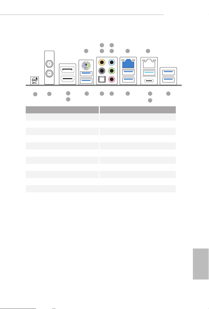
1.4 I/O Panel
254
31
Z490 Taichi
6
7
17
18
No. Description No. Description
1 PS/2 Mouse/Keyboard Port 10 USB 3.2 Gen2x2 Type-C Port
2 Central / Bass (Orange) (USB32_TC_1)
3 Rear Speaker (Black) 11 USB 3.2 Gen2 Ports (USB31_1_2)
4 Line In (Light Blue) 12 Microphone (Pink)
5 Front Speaker (Lime)* 13 Optical SPDIF Out Port
6 2.5G LAN RJ-45 Port 14 USB 3.2 Gen1 Ports (USB3_12)
(Dragon RTL8125BG)** 15 DisplayPort 1.4
7 LAN RJ-45 Port (Intel® I219V)*** 16 HDMI Port
8 USB 3.2 Gen1 Ports (USB3_4_5)**** 17 Antenna Ports (on I/O Panel Shield)
9 USB 3.2 Gen1 Type-A Port 18 BIOS Flashback Button
(USB3_3)
15
16
121314
11
9 8
10
11
English
Page 19
* If you use a 2-channel spea ker, please connect the s peaker’s plug into “Front Speaker Jack”. See the table below
for connection d etails in accordance w ith the type of speaker you use.
Audio Output
Channels
Front Speaker
(No. 5)
Rear Speaker
(No. 3)
Central / Bass
(No. 2)
Line In
(No. 4)
2 V -- -- --
4 V V -- --
6 V V V --
8 V V V V
**ere are two LEDs on each LAN port. Plea se refer to the table below for the LA N port LED indic ations.
ACT/LINK LED
SPEED LED
LAN Por t
Activity / Link LED Speed LED
Status Description Status Description
O No Link O 10Mbps connection
Blinking Data Activity Orange
100Mbps/1Gbps
connection
On Link Green 2.5Gbps connection
*** ere are two LEDs on each LAN port. Please refer to the table below for the LAN port LED indications.
ACT/LINK LED
SPEED LED
English
12
LAN Por t
Activity / Link LED Speed LED
Status Description Status Description
O No Link O 10Mbps connection
Blinking Data Activity Orange 100Mbps connection
On Link Green 1Gbps connection
**** ACPI wake-up function is not supported on USB3_ 4_5 ports.
Page 20

1.5 WiFi-802.11ax Module and ASRock WiFi 2.4/5 GHz
Antenna
WiFi-802.11ax + BT Module
is motherboard comes with an exclusive WiFi 802.11 a/b/g/n/ax + BT v5.1
module (pre-installed on the rear I/O panel) that oers support for WiFi 802.11 a/b/
g/n/ax connectivity standards and Bluetooth v5.1. WiFi + BT module is an easy-to-
use wireless local area network (WLAN) adapter to support WiFi + BT. Bluetooth
v5.1 standard features Smart Ready technology that adds a whole new class of
functionality into the mobile devices. BT 5.1 also includes Low Energy Technology
and ensures extraordinary low power consumption for PCs. e 2T2R WiFi
solution sets a WiFi high speed standard and oers max link rate up to 2.4Gbps.
* e transmission speed may vary according to the environment.
Z490 Taichi
ASRock WiFi 2.4/5 GHz Antenna
English
13
Page 21

Chapter 2 Installation
is is an ATX form factor motherboard. Before you install the motherboard, study
the conguration of your chassis to ensure that the motherboard ts into it.
Pre-installation Precautions
Take note of the following precautions before you install motherboard components
or change any motherboard settings.
Make sure to unplug the power cord before installing or removing the motherboard
•
components. Failure to do so may cause physical injuries and damages to motherboard
components.
In order to avoid damage from static electricity to the motherboard’s components,
•
NEVER place your motherboard directly on a carpet. Also remember to use a grounded
wrist strap or touch a safety grounded object before you handle the components.
Hold components by the edges and do not touch the ICs.
•
Whenever you uninstall any components, place them on a grounded anti-static pad or
•
in the bag that comes with the components.
When placing screws to secure the motherboard to the chassis, please do not over-
•
tighten the screws! Doing so may damage the motherboard.
English
14
Page 22
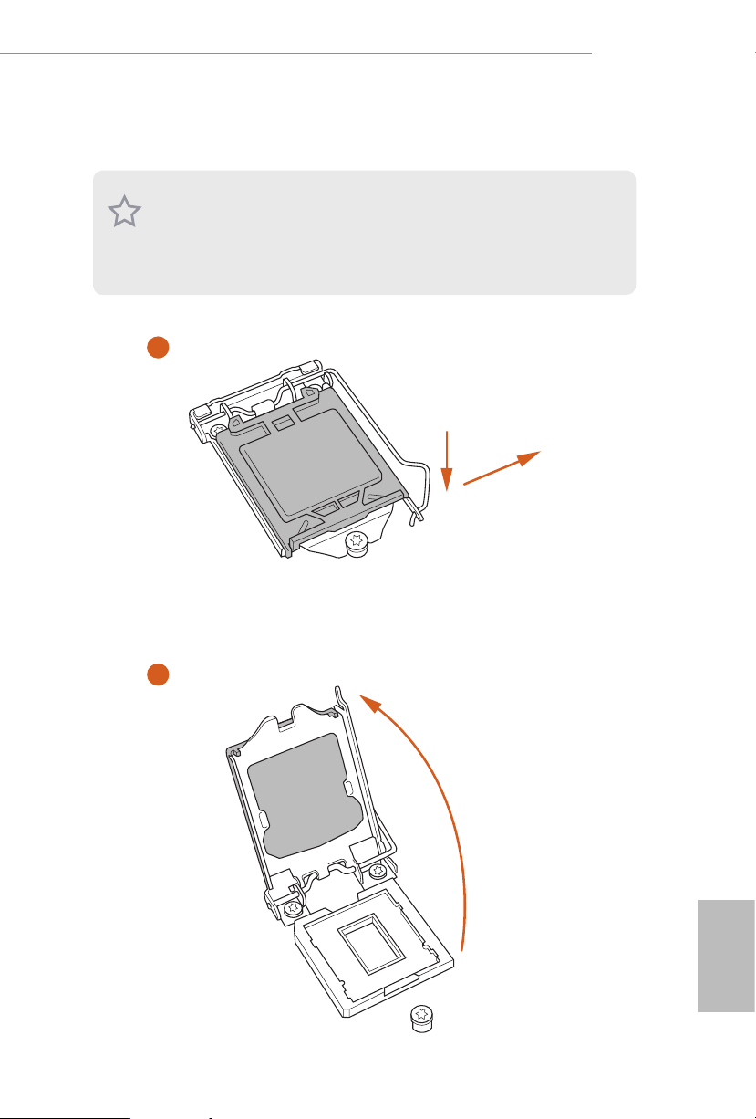
2.1 Installing the CPU
1
1. Before you insert the 1200-Pin CPU into the socke t, please check if the Pn P cap is on the
socket, if the CPU surface is unclean, or if there are any bent pins in the sock et. Do not
force to in sert the CPU into the socket if above situation is found . Otherwise, the CPU
will be seriously damaged.
2. Unplug all power c ables before in stalling the CPU.
Z490 Taichi
A
B
2
15
English
Page 23
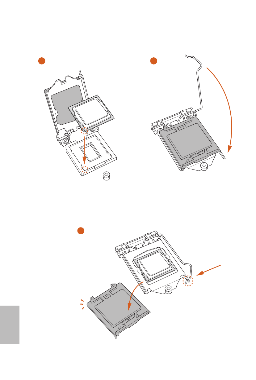
3
5
4
English
16
Page 24

Please save and replace the cover if the processor i s removed. e cover must be placed if
you wish to return the motherboard for aer service.
Z490 Taichi
17
English
Page 25
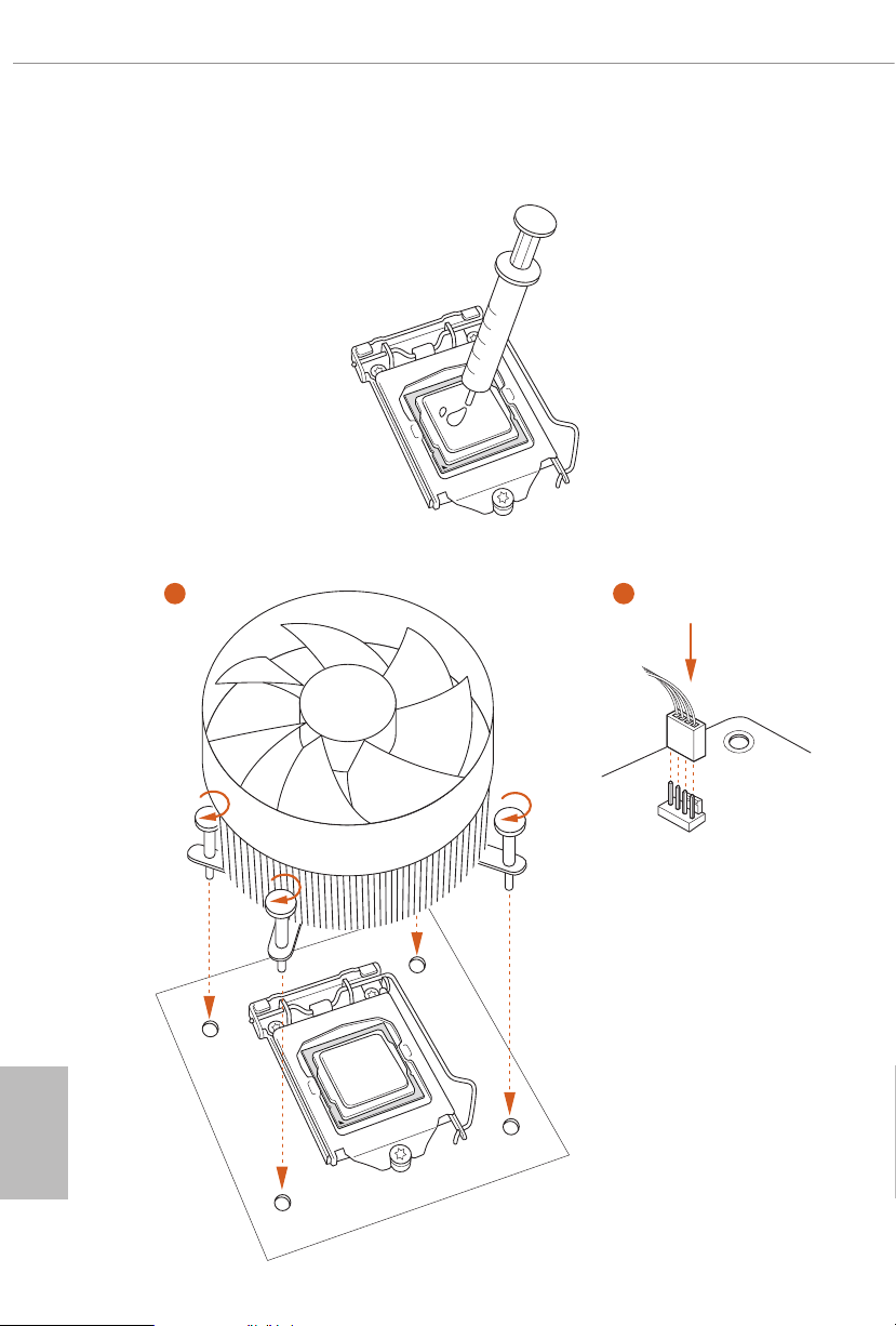
2.2 Installing the CPU Fan and Heatsink
1 2
English
18
CPU_FAN
Page 26
2.3 Installing Memory Modules (DIMM)
is motherboard provides four 288-pin DDR4 (Double Data Rate 4) DIMM slots,
and supports Dual Channel Memory Technology.
1. For dual channel cong uration , you always need to in stall identical (the same b rand,
speed , size and chip-type) DDR4 DIMM pairs.
2. It is unable to activate Dual Channel Memor y Technolog y with only one or three memor y
module installed.
3. It is not allowed to install a DDR, DDR2 or DDR3 memory module into a DDR4 sl ot;
otherwise , this motherboard and DIM M may be damaged.
Dual Channel Memory Conguration
Priority DDR4_A1 DDR4_A2 DDR4_B1 DDR4_B2
1 Populated Populated
2 Populated Populated Populated Populated
e DIMM only ts in one correct orie ntation. It will cause permanent dam age to the
motherboard and the DIMM if you force the DIMM into the slot at incorrect orientation.
Z490 Taichi
19
English
Page 27
1
2
English
20
3
Page 28

2.4 Expansion Slots (PCI Express Slots)
ere are 5 PCI Express slots on the motherboard.
Before installing an ex pansion card, please make sure that the power supply is switched o
or the power cord is unplug ged. Pl ease re ad the documentation of the expansion card and
make necessary hardware settings for the card before you start the installation.
PCIe slots:
PCIE1 (PCIe 3.0 x16 slot) is used for PCI Express x16 lane width graphics cards.
PCIE2 (PCIe 3.0 x1 slot) is used for PCI Express x1 lane width cards.
PCIE3 (PCIe 3.0 x16 slot) is used for PCI Express x8 lane width graphics cards.
PCIE4 (PCIe 3.0 x1 slot) is used for PCI Express x1 lane width cards.
PCIE5 (PCIe 3.0 x16 slot) is used for PCI Express x4 lane width graphics cards.
PCIe Slot Congurations
PCIE1 PCIE3 PCIE5
Single Graphics Card x16 N/A N/A
Z490 Taichi
Two Graphics Cards in
CrossFireXTM or SLITM
Mode
ree Graphics Cards in
3-Way CrossFireXTM Mode
For a better ther mal environme nt, ple ase connect a ch assis fan to the motherboard’s
chassis fan connector (CHA_ FA N1~6/WP) when u sing multiple graphics cards.
x16 x8 N/A
x16 x8 x4
English
21
Page 29
2.5 MOS Heatsink Height
MOS-N Heatsink Height
42.0 mm
English
22
37.5 mm
30.8 mm
42.0 mm
Page 30
2.6 Jumpers Setup
e illustration shows how jumpers are setup. When the jumper cap is placed on
the pins, the jumper is “Short”. If no jumper cap is placed on the pins, the jumper is
“O pen”.
Z490 Taichi
Clear CMOS Jumper
(CLRCMO S1)
(see p.9, No. 28)
CLRCMOS1 allows you to clear the data in CMOS. e data in CMOS includes
system setup information such as system password, date, time, and system setup
parameters. To clear and reset the system parameters to default setup, please
turn o the computer and unplug the power cord, then use a jumper cap to short
the pins on CLRCMOS1 for 3 seconds. Please remember to remove the jumper
cap aer clearing the CMOS. If you need to clear the CMOS when you just nish
updating the BIOS, you must boot up the system rst, and then shut it down
before you do the clear-CMOS action.
2-pin Jumper
Short: Clear CMOS
Open: Default
23
English
Page 31

2.7 Onboard Headers and Connectors
1
Onboard headers and connectors are NOT jump ers. Do NOT place jumper caps over these
heade rs and connectors. Placing jumper caps over the headers and connectors will cause
permanent damage to the motherboard.
System Panel Header
(9-pi n PANEL1)
(see p.9, No. 21)
PWRBTN (Power Button):
Connec t to the power button on the ch assi s front panel. You may congure the way to tur n
o your system using the power button.
RESET (Reset B utton):
Connec t to the reset button on the ch assi s front panel. P ress the reset button to re start the
computer if the computer f reezes and fails to per form a normal restar t.
PLED (Syste m Power LED):
Connec t to the power status indicator on the chas sis front panel. e LED i s on when the
system is operating. e LED keeps blinking when the system is in S1/S3 sleep state. e
LED is o when the system is in S4 slee p state or powered o (S5).
HDLED (Ha rd Drive Activity LED):
Connec t to the hard drive ac tivity LED on the chassis front panel. e LED is on when the
hard drive is reading or wr iting data.
e front panel de sign may dier by chassis. A front panel module mainly consists of powe r
button, reset button , power LED, hard dr ive activity LED, speaker and etc. When connecting your ch assi s front panel module to thi s header, make sure the wire a ssignments and the
pin assignments are matched correctly.
PLED+
PLED-
HDLED-
HDLED+
PWRBTN#
GND
GND
RESET#
GND
Connect the power
button, reset button and
system status indicator on
the chassis to this header
according to the pin
assignments below. Note
the positive and negative
pins before connecting
the cables.
English
24
Page 32

Z490 Taichi
1
+5V
DUMMY
PLED+
PLED+
PLED-
DUMMY
SPEAKER
DUMMY
GND
GND
P+
P-
USB_PWR
P+
P-
USB_PWR
1
Power LED and Speaker
Header
(7-pin SPK_PLED1)
(see p.9, No. 20)
Serial ATA3 Connectors
(SATA3_0_1:
see p.9, No. 14)
(SATA3_2_3:
see p.9, No. 15)
(SATA3_4_5:
see p.9, No. 16)
(SATA3_A1_A2:
see p.9, No. 17)
SATA3_2SATA3_4
SATA3_A1 SATA3_0
Please connect the
chassis power LED and
the chassis speaker to this
header.
ese eight SATA3
connectors support SATA
data cables for internal
storage devices with up to
6.0 Gb/s data transfer rate.
* M2_ 2, SATA3_0 and
SATA3_3SATA3_5
SATA3_1 share lanes. If
either one of them is in
use, the others will be
disabled.
* M2_ 3, SATA3_4 and
SATA3_5 share lanes. If
either one of them is in
use, the others will be
SATA3_A2 SATA3_1
disabled.
* M2_ 3, SATA3_4,
SATA3_5 and USB32_
TC_1 share lanes. If
either one of them is in
use, USB32_TC_1 will
downgrade to 16 Gb/s
max.
*To minimize the boot
time, use Intel® Z490
SATA ports (SATA3_0)
for your SSDs.
USB 2.0 Headers
(9-pin USB_1_2)
(see p.9, No. 26)
(9-pin USB_3_4)
(see p.9, No. 25)
ere are two headers
on this motherboard.
Each USB 2.0 header can
support two ports.
English
25
Page 33

USB 3.2 Gen1 Headers
J_SENSE
OUT2_L
1
MIC_RET
PRESENCE#
GND
OUT2_R
MIC2_R
MIC2_L
OUT_RET
1
IntA_PB_SSTX+
IntA_PB_SSRX+
A_SSRX+
A_SSTX+
ype-C Cable
(19-pin USB3_6_7)
(see p.9, No. 10)
Dummy
IntA_PB_D+
IntA_PB_D-
GND
IntA_PB_SSTX-
GND
IntA_PB_SSRX-
VbusV
IntA_PA_D+
IntA_PA_D-
GND
IntA_P
IntA_PA_SSTX-
GND
IntA_P
IntA_PA_SSRX-
VbusV
ere are two headers on
this motherboard. Each
USB 3.2 Gen1 header can
support two ports.
(19-pin USB3_8_9)
(see p.9, No. 9)
Front Panel Type C USB
3.2 Gen2 Header
(20-pin USB31_TC_2)
(see p.9, No. 12)
Front Panel Audio Header
(9-pin HD_ AUDIO1)
(see p.9, No. 34)
Vbus
IntA_PA_SSRX-
IntA_PA_SSRX+
GND
IntA_PA_SSTX-
IntA_PA_SSTX+
GND
IntA_PA_D-
IntA_PA_D+
USB T
VbusVbus
IntA_PB_SSRX-
IntA_PB_SSRX+
GND
IntA_PB_SSTX-
IntA_PB_SSTX+
GND
IntA_PB_D-
IntA_PB_D+
Dummy
1
ere is one Front
Panel Type C USB 3.2
Gen2 Header on this
motherboard. is header
is used for connecting a
USB 3.2 Gen2 module for
additional USB 3.2 Gen2
ports.
is header is for
connecting audio devices
to the front audio panel.
English
26
High Denition Audio supports Jack Sens ing, but the panel wire on the chassis mus t support HDA to function correctly. Ple ase fol low the instructions in our manual and chassis
manual to install your system.
Page 34

Z490 Taichi
GND
OL
GND
OL
GND
OL
1
GND
OL
1
FAN_SPEED_CONTROL
1 2 3 4
Chassis/Water Pump Fan
Connectors
(4-pin CHA_FAN1/WP)
(see p.9, No. 35)
(4-pin CHA_FAN2/WP)
(see p.9, No. 31)
(4-pin CHA_FAN3/WP)
(see p.9, No. 19)
(4-pin CHA_FAN4/WP)
(see p.9, No. 30)
(4-pin CHA_FAN5/WP)
(see p.9, No. 13)
(4-pin CHA_FAN6/WP)
(see p.9, No. 18)
CPU Fan Connector
(4-pin CPU_FAN1)
(see p.9, No. 3)
FAN_VOLTAGE
FAN_SPEED
FAN_SPEED_CONTR
1 2 3 4
2
3
4
FAN_VOLTAGE
FAN_SPEED
FAN_SPEED_CONTR
1 2 3 4
2
3
4
CPU_FAN_SPEED
FAN_VOLTAGE
GND
FAN_VOLTAGE
CHA_FAN_SPEED
FAN_SPEED_CONTR
FAN_VOLTAGE
CHA_FAN_SPEED
FAN_SPEED_CONTR
is motherboard
provides six 4-Pin water
cooling
chassis
fan
connectors. If you plan to
connect a 3-Pin
chassis
water cooler fan, please
connect it to Pin 1-3.
is motherboard
provides a 4-Pin CPU fan
(Quiet Fan) connector.
If you plan to connect a
3-Pin CPU fan, please
connect it to Pin 1-3.
English
27
Page 35

CPU/Water Pump Fan
FA
4
1
8 5
1
Connector
(4-pin CPU_FAN2/
WP_ 3A)
(see p.9, No. 4)
N_SPEED_CONTROL
CPU_FAN_SPEED
FAN_VOLTAGE
GND
is motherboard
4
provides a 4-Pin water
3
2
cooling CPU fan
1
connector. If you plan
to connect a 3-Pin CPU
water cooler fan, please
connect it to Pin 1-3.
English
ATX Power Connector
(24-p i n ATX PWR1)
(see p.9, No. 8)
ATX 12V Power
Connectors
(8-pin ATX12V1)
(see p.9, No. 1)
(8-pin ATX12V2)
(see p.9, No. 2)
underbolt AIC
Connectors
(5-p i n TB1)
(see p.9, No. 33)
12
24
is motherboard pro-
vides a 24-pin ATX power
connector. To use a 20-pin
ATX power supply, please
plug it along Pin 1 and Pin
1
13
13.
is motherboard
provides two 8-pin ATX
12V power connectors. To
use a 4-pin ATX power
supply, please plug it along
Pin 1 and Pin 5.
*Warning: Please make
sure that the power cable
connected is for the CPU
and not the graphics
card. Do not plug the
PCIe power cable to this
connector.
Please connect a underbolt™
add-in card (AIC) to the
underbolt AIC connector via
the GPIO cable.
*Please install the underbolt™
AIC card to PCIE3 (default
slot).
28
Page 36

Z490 Taichi
1
SPI_DQ3
#
1
1
DO_ADDR
D
1
SPI TPM Header
(13 -pi n SPI_T PM _J1)
(see p.9, No. 27)
RGB LED Headers
(4-p i n RGB_LED1)
(see p.9, No. 29)
(4-pi n RGB _LED2)
(see p.9, No. 11)
Addressable LED Headers
(3-pin A DDR_LE D1)
(see p.9, No. 32)
(3-pin A DDR_LE D2)
(see p.9, No. 7)
+3.3V
Dummy
CLK
RSMRST#
SPI_MISO
SPI_CS0
SPI_DQ2
12V GRB
B
R
G
12V
DO_ADDR
VOUT
GND
VOUT
1
SPI_MOSI
RST#
TPM_PIRQ
SPI_TPM_CS
GND
GN
is connector supports SPI
Trusted Platform Module (TPM)
system, which can securely store
keys, digital certicates, pass-
words, and data. A TPM system
also helps enhance network
security, protects digital
identities, and ensures platform
integrity.
ese two RGB headers are used
to connect RGB LED extension
cable which allows
users to choose from various LED
lighting eects.
Caution: Never install the RGB
LED cable in the wrong orienta-
tion; otherwise, the cable may
be damaged.
*Please refer to page 67 for
further instructions on these two
headers.
ese two
are used to connect
Addressable
Addressable
headers
LED extension cable which
allows users to choose from
various LED lighting eects.
Caution: Never install the
Addressable LED cable in the
wrong orientation; otherwise,
the cable may be damaged.
*Please refer to page 68 for
further instructions on this
header.
English
29
Page 37

2.8 Smart Switches
e motherboard has four smart switches: Power Button, Reset Button, Clear
CMOS Buttons and BIOS Flashback Button, allowing users to quickly turn on/o
the system, reset the system, clear the CMOS values or ash the BIOS.
Power Button
(P WR BTN1)
(see p.9, No. 22)
Reset Button
(R STB T N1)
(see p.9, No. 24)
Clear CMOS Button
(CLRCBTN1)
(see p.9, No. 23)
Power
Reset
Power Button allows users
to quickly turn on/o the
system.
Reset Button allows
users to quickly reset the
system.
Clear CMOS Button
allows users to quickly
clear the CMOS values.
English
30
Page 38

Z490 Taichi
BIOS Flashback Button
(BIOS_FB1)
BIOS Flashback Switch allows users
to ash the BIOS.
(see p.11, No. 18)
ASRock BIOS Flashback feature allows you to update BIOS without poweri ng on the system, even
without CPU.
To use the USB BIOS Flashback function, Plea se follow the steps below.
1. Download the latest BIOS le from ASRock's website : http://www.asrock.com.
2. Copy t he BIOS le to your USB ash drive. Please make sure the le system of
your USB ash drive must be FAT32.
3. Extract BIOS le from the zip le.
4. Rename the le to “creative.rom” and save it to the root director y of X: USB ash drive.
5. Plug the 24 pin power connector to t he motherboard. en turn on the power supply's AC
switch.
*ere is no need to power on t he system.
6. en plug your USB drive to the USB BIOS Flashback port.
7. Press the BIOS Flashback Switch for about three seconds. en the LED starts to blink.
8. Wait unti l the LED stops blink ing, i ndicating that BIOS ashing has been completed.
*If the LED light turns solid green, this means that the BIOS Flashback is not
operating properly. Please make sure that you plug t he USB drive to the USB BIOS Flashback
port.
USB BIOS Flashback port
English
31
Page 39

2.9 Dr. Debug
Dr. Debug is used to provide code information, which makes troubleshooting even
easier. Please see the diagrams below for reading the Dr. Debug codes.
Code Description
0x10 PEI_COR E_STARTE D
0x11 PEI_CAR_CPU_INIT
0x15 PEI_CAR_NB_INIT
0x19 PEI_CAR_SB_INIT
0x 31 PEI_MEMORY_INSTALLED
0x32 PEI_CPU_INIT
0x33 PEI_CPU_CACHE_INIT
0x34 PEI_CPU_AP_INIT
0x35 PEI_CPU_BSP_SELECT
English
32
0x36 PEI_CPU_SMM_INIT
0x37 PEI_MEM_NB_INIT
0x3B PEI_MEM_SB_INIT
0x4F PEI_DXE_IPL_STARTED
0x60 DXE_CORE_STARTED
0x61 DXE_NVRAM_INIT
0x62 DXE_SBRU N_I NIT
Page 40

0x63 DXE _CPU_ INIT
0x68 DXE_NB_HB_INIT
0x69 DXE_NB_INIT
0x6A DXE_NB_SMM_INIT
0x70 DXE_SB_I NIT
0x71 DXE_SB_SMM_INIT
0x72 DXE_SB_DEVICES_INIT
0x78 DXE_ACPI_INIT
0x79 DXE _CSM _INIT
Z490 Taichi
0x90 DXE_BDS_STARTED
0x91 DXE_BDS_CONNECT_DRIVERS
0x92 DXE_PCI_BUS_BEGIN
0x93 DXE_PCI_BUS_HPC_INIT
0x94 DXE_PCI_BUS_ENUM
0x95 DXE_PCI_BUS_REQUEST_RESOURCES
0x96 DXE_PCI_BUS_ASSIGN_RESOURCES
0x97 DXE_CON_OUT_CONNECT
0x98 DXE_CON_IN_CONNECT
English
33
Page 41

0x99 DXE_SIO_I NIT
0x 9A DXE_USB_BEGIN
0x9B DXE_USB_ R ESET
0x9C DXE_USB_DETECT
0x9D DXE_USB_ENABLE
0xA0 DXE_IDE_BEGIN
0xA1 DXE_IDE_RESET
0xA2 DXE_IDE _DETECT
0xA3 DXE_IDE_ENABLE
0xA4 DXE_SCSI_BEGIN
0xA5 DXE _SC SI _RESET
English
34
0xA6 DXE_SCSI_DETECT
0xA7 DX E_SCSI_ENA BL E
0xA8 DX E_SET UP_VER IFYING_ PASSWORD
0xA9 DXE_SETUP_START
0xAB DXE_SETUP_INPUT_WAIT
0xAD DXE _READY_TO_BOOT
0xAE DXE_LEGACY_BOOT
Page 42

0xAF DXE_EXIT_BOOT_SERVICES
0xB0 RT_SET_VIRTUAL_ADDRESS _MAP_BEGIN
0x B1 RT_SET_VIRTUAL_ADDRESS_MAP_END
0xB2 DXE _LEGACY_OPROM _IN IT
0xB3 DXE_RESET_SYSTEM
0xB4 DXE_USB_HOTPLUG
0xB5 DXE_PCI_BUS _HOTPLUG
0xB6 DXE_NVRAM_CLEANUP
0xB7 DXE_CONFIGURATION_RESET
Z490 Taichi
0xF0 PEI _REC OVERY_AUTO
0xF1 PEI_RECOVERY_USER
0xF2 PEI_RECOV ERY_STARTED
0xF3 PEI_RECOVERY_CAPSULE_FOUND
0xF4 PEI_ RECOVERY_CAPSULE_LOADED
0xE0 PEI_S3_STARTED
0xE1 PEI_S3_BOOT_SCRIPT
0xE2 PEI_S3_VIDEO_REPOST
English
35
Page 43

0xE3 P E I _S 3_OS _WAK E
0x50 PEI_MEMORY_INVALID_TYPE
0x53 PEI_MEMORY_NOT_DETECTED
0x55 PEI_MEMORY_NOT_INSTALLED
0x57 PEI_CPU_M ISMATCH
0x58 PEI_CPU_SELF_TEST_FAILED
0x59 PEI_CPU_NO_MICROCODE
0x5A PEI_CPU_ERROR
0x5B PEI_R ESET_NOT_ AVAILABLE
0xD0 DXE _CPU_ERROR
0x D1 DXE_NB_ERROR
English
36
0xD2 DXE_SB_ERROR
0xD3 DXE_ARCH_PROTOCOL_NOT_AVAILABLE
0xD4 DXE_PCI_BUS_OUT_OF_RESOURCES
0xD5 DX E _LEGAC Y_OPROM_NO_ SPACE
0xD6 DXE_NO_CON_OUT
0xD7 DXE_NO_CON_IN
Page 44

0xD8 DXE_I NVALID_ PASSWORD
0xD9 DXE_BOOT_OPTION_LOAD_ERROR
0x DA DXE_BOOT_OPTION_FAILED
0xDB DXE_FLASH_UPDATE_FAILED
0xDC DX E _RE SET_NOT_AVA IL ABLE
0xE8 PEI_MEMORY_S3_RESUME_FAILED
0xE9 PEI_S3_RESUME_PPI_NOT_FOUND
0xEA PEI_S3_ BOOT_ SCRIPT_ ERROR
0xEB PEI_S3_OS_WAKE_ERROR
Z490 Taichi
37
English
Page 45

2.10 SLITM Operation Guide
is motherboard supports NVIDIA® SLITM (Scalable Link Interface) technology
that allows you to install up to two identical PCI Express x16 graphics cards.
Requirements
1. You should only use identic al SLITM-ready g raphics cards that are NV IDIA® certied.
2. Make sure that your graphics card driver supports NVI DIA® SLITM technology.
Download the drivers from the N VIDIA® website: www.nvidia.com
3. Make sure that your power supply unit (PSU) can provide at least the minimum
power your syste m require s. It is recommended to use a NVIDIA® certied PSU.
Please refer to the NVIDIA® website for details.
2.10.1 Installing Two SLITM-Ready Graphics Cards
Step 1
Insert one graphics card into PCIE1 slot
and the other graphics card to PCIE3 slot.
Make sure that the cards are properly
seated on the slots.
English
38
Step 2
If required, connect the auxiliary power
source to the PCI Express graphics cards.
Page 46

SLI_HB_Bridge_2S Card
ASRock SLI_HB_Bridge_2S Card
Step 3
Align and insert the ASRock SLI_HB_
Bridge_2S Card to the goldngers on each
graphics card. Make sure the ASRock SLI_
HB_Bridge_2S Card is rmly in place.
Step 4
Connect a VGA cable or a DVI cable to the
monitor connector or the DVI connector of
the graphics card that is inserted to PCIE1
slot.
Z490 Taichi
39
English
Page 47

2.10.2 Driver Installation and Setup
Install the graphics card drivers to your system. Aer that, you can enable the
Multi-Graphics Processing Unit (GPU) in the N VIDIA® nView system tray utilit y.
Please follow the below procedures to enable the multi-GPU.
For SLITM mode
Step 1
Double-click the NVIDIA Control Panel
icon in the Windows® sy stem tray.
Step 2
In the le pane, click Set SLI and PhysX
conguration. en select Maximize 3D
performance and click Apply.
Step 3
Reboot your system.
Step 4
You can freely enjoy the benets of SLITM.
English
40
Page 48

Z490 Taichi
2.11 CrossFireXTM , 3-Way CrossFireXTM and Quad CrossFireXTM
Operation Guide
is motherboard supports CrossFireXTM, 3-way CrossFireXTM and Quad
CrossFireXTM that allows you to install up to three identical PCI Express x16
graphics cards.
1. You should only use identical CrossFireXTM-ready g raphics cards that are AM D
certied.
2. Make sure that your graphics card driver supports AMD CrossFire XTM technology.
Download the drivers from the A MD’s website: www.amd.com
3. Make sure that your power supply unit (PSU) can provide at least the minimum
power your syste m require s. It is recommended to use a AMD certied PSU. Plea se
refer to the AMD’s website for d etail s.
4. If you pair a 12-pipe CrossFireXTM Edition card with a 16-pipe card, both cards will
operate a s 12-pipe cards while in CrossFireXTM mode.
5. Dierent CrossFireXTM cards may require dierent method s to enable CrossFireXTM. Please refer to A MD graphics card manuals for de tailed installation guide.
2.11.1 Installing Two CrossFireXTM-Ready Graphics Cards
CrossFire Bridge
Step 1
Insert one graphics card into PCIE1 slot
and the other graphics card to PCIE3 slot.
Make sure that the cards are properly
seated on the slots.
Step 2
Connect two graphics cards by installing
a CrossFire Bridge on the CrossFire Bridge
Interconnects on the top of the graphics
cards. (e CrossFire Bridge is provided
with the graphics card you purchase, not
bundled with this motherboard. Please
refer to your graphics card vendor for
deta ils .)
English
41
Page 49

Step 3
Connect a VGA cable or a DVI cable to the
monitor connector or the DVI connector of
the graphics card that is inserted to PCIE1
slot.
English
42
Page 50

2.11.2 Installing Three CrossFireXTM-Ready Graphics Cards
Step 1
Insert one graphics card into PCIE1 slot,
another graphics card to PCIE3 slot, and
the other graphics card to PCIE5 slot.
Make sure that the cards are properly
seated on the slots.
Step 2
Use one CrossFire Bridge to connect
CrossFire Bridge
the graphics cards on PCIE1 and PCIE3
slots, and use the other CrossFire Bridge
to connect the graphics cards on PCIE3
and PCIE5 slots. (e CrossFire Bridge
is provided with the graphics card
you purchase, not bundled with this
motherboard. Please refer to your graphics
card vendor for details.)
Z490 Taichi
Step 3
Connect a VGA cable or a DVI cable to the
monitor connector or the DVI connec-
tor of the graphics card that is inserted to
PCIE1 slot.
English
43
Page 51

2.11.3 Driver Installation and Setup
Step 1
Power on your computer and boot into OS.
Step 2
Remove the AMD drivers if you have any VGA drivers installed in your system.
e Catalyst Unins talle r is an optional do wnload. We recommend us ing this utility
to uninstall any previously installed Catalyst drivers prior to installation. Pl ease
check A MD’s website for AMD driver update s.
Step 3
Install the required drivers and CATALYST Control Center then restart your
computer. Please check AMD’s website for details.
Step 4
Double-click the AMD Catalyst Control
AMD Catalyst Control Center
Center icon in the Windows® sy stem tray.
Step 5
In the le pane, click Performance and
then AMD CrossFireXTM. en select
Enable AMD CrossFireX and click Apply.
Select the GPU number according to your
graphics card and click Apply.
English
44
Page 52

Z490 Taichi
2.12 M.2_SSD (NGFF) Module Installation Guide (M2_1)
e Ultra M.2 Socket (M2_1) supports type 2280 M.2 PCI Express module up to Gen3 x4 (32
Gb/s).
Installing the M.2_SSD (NGFF) Module
Step 1
Prepare a M.2_SSD (NGFF) module
and the screw.
Step 2
Depending on the PCB type and
length of your M.2_SSD (NGFF)
module, nd the corresponding nut
location to be used.
No. 1
Nut Location A
PCB Length 8cm
Module Type Type2280
English
45
Page 53

Step 3
1
2
1
1
Before installing a M.2 (NGFF) SSD
module, please loosen the screws to
remove the M.2 heatsink.
*Please remove the protective lms
1
1
on the bottom side of the M.2
heatsink before you install a M.2
SSD module.
1
Step 4
Align and gently insert the M.2
(NGFF) SSD module into the M.2
slot. Please be aware that the M.2
(NGFF) SSD module only ts in one
orientation.
A
English
46
A
o
20
Step 5
Tighten the screw with a screwdriver
to secure the module into place.
Please do not overtighten the screw
NUT1NUT2
as this might damage the module.
Page 54

M.2_SSD (NGFF) Module Support List (M2_1)
Vendor Interface P/N
ADATA PCIe3 x4 ASX7000NP-128GT-C
ADATA PCIe3 x4 ASX8000NP-256GM-C
ADATA PCIe3 x4 ASX7000NP-256GT-C
ADATA PCIe3 x4 ASX8000NP-512GM-C
ADATA PCIe3 x4 ASX7000NP-512GT-C
Apacer PCIe3 x4 AP240GZ280
Corsair PCIe3 x4 CSSD-F240GBMP500
Intel PCIe3 x4 SSDPEKKF256G7
Intel PCIe3 x4 SSDPE KKF512G7
Kingston PCIe3 x4 SKC1000/480G
Kingston PCIe2 x4 SH2280S3/480G
OCZ PCIe3 x4 RVD400-M2280-512G (NVME)
PAT R IOT PCIe3 x4 PH240GPM280SSDR NVME
Plextor PCIe3 x4 PX-128M8PeG
Plextor PCIe3 x4 PX-1TM 8PeG
Plextor PCIe3 x4 PX-256M8PeG
Plextor PCIe3 x4 PX-512M8Pe G
Plextor PCIe PX-G256M6 e
Plextor PCIe PX-G512M6e
Samsung PCIe3 x4 SM961 MZVPW128HEGM (NVM)
Samsung PCIe3 x4 PM961 MZVLW128HEGR (NVME)
Samsung PCIe3 x4 960 EVO (MZ-V6E250) (NVME)
Samsung PCIe3 x4 960 EVO (MZ-V6E250BW) (NVME)
Samsung PCIe3 x4 SM951 (N VME)
Samsung PCIe3 x4 SM951 (MZHPV256HDGL)
Samsung PCIe3 x4 SM951 (MZHPV512HDGL)
Samsung PCIe3 x4 SM951 (N VME)
Samsung PCIe x4 XP941-512G (MZHPU512HCGL)
SanDisk PCIe SD6PP4M-12 8G
SanDisk PCIe SD6PP4M-256G
TEAM PCIe3 x4 TM8FP2240G 0C101
TEAM PCIe3 x4 TM8FP2480GC110
WD PCIe3 x4 WDS256G1X0C-00ENX0 (NVME)
WD PCIe3 x4 W DS512G1X0 C-0 0ENX0 (NVME)
Z490 Taichi
For the latest updates of M.2_SSD (NFGG) module support list, please visit our website for
details: http://www.asrock.com
English
47
Page 55

2.13 M.2_SSD (NGFF) Module Installation Guide (M2_2)
The M.2, a lso known as the Next Generation Form Factor (NGFF), is a sma ll size a nd
versatile card edge connec tor t hat aims to replace mPCIe and mSATA. The Ult ra M.2
Socket (M2_2) supports type 2260/2280 M.2 PCI Express module up to Gen3 x4 (32 Gb/s).
* M2_ 2, SATA3_0 and SATA3_1 share lanes. If either one of them is in use, the others will
be disabled.
Installing the M.2_SSD (NGFF) Module
Step 1
is motherboard supports M.2_SSD
(NGFF) module t ype 2260 and 2280
only. Prepare a proper PCB lenth of
module, the screw and the stando.
Step 2
Depending on the PCB type and
2
1
length of your M.2_SSD (NGFF)
module, nd the corresponding nut
location to be used.
English
48
A
B
No. 1 2
Nut Location A B
PCB Length 6cm 8cm
Module Type Ty pe 2260 Type 228 0
Page 56

Z490 Taichi
1
2
1
1
Step 3
Before installing a M.2 (NGFF) SSD
module, please loosen the screws to
remove the M.2 heatsink.
*Please remove the protective lms
1
1
on the bottom side of the M.2
heatsink before you install a M.2
1
SSD module.
Step 4
Prepare the M.2 stando that comes
with the package. en hand tighten
the stando into the desired nut
location on the motherboard. Align
AB
and gently insert the M.2 (NGFF)
SSD module into the M.2 slot. Please
be aware that the M.2 (NGFF) SSD
module only ts in one orientation.
AB
o
20
Step 5
Tighten the screw with a screwdriver
to secure the module into place.
Please do not overtighten the screw
NUT1NUT2B
as this might damage the module.
English
49
Page 57

English
M.2_SSD (NGFF) Module Support List (M2_2)
Vendor Interface P/N
ADATA SATA3 AXNS381E-128GM-B
ADATA SATA3 AXNS3 81E-256GM-B
ADATA SATA3 ASU800NS38-256GT-C
ADATA SATA3 ASU800NS38-512GT-C
ADATA PCIe3 x4 ASX7000NP-128GT-C
ADATA PCIe3 x4 ASX8000NP-256GM-C
ADATA PCIe3 x4 ASX7000NP-256GT-C
ADATA PCIe3 x4 ASX8000NP-512GM-C
ADATA PCIe3 x4 ASX7000NP-512GT-C
Apacer PCIe3 x4 AP240GZ280
Corsair PCIe3 x4 CSSD-F240GBMP500
Crucial SATA3 CT120M500SSD4
Crucial SATA3 CT240M500SSD4
Intel SATA3 Intel SSDSCKGW080A401/80G
Intel PCIe3 x4 SSDPEKKF256G7
Intel PCIe3 x4 SSDPE KKF512G7
Kingston SATA3 SM2280S3
Kingston PCIe3 x4 SKC1000/480G
Kingston PCIe2 x4 SH2280S3/480G
OCZ PCIe3 x4 RVD400-M2280-512G (NVME)
PAT R IOT PCIe3 x4 PH240GPM280SSDR NVME
Plextor PCIe3 x4 PX-128M8PeG
Plextor PCIe3 x4 PX-1TM 8PeG
Plextor PCIe3 x4 PX-256M8PeG
Plextor PCIe3 x4 PX-512M8Pe G
Plextor PCIe PX- G256M6 e
Plextor PCIe PX-G512M6e
Samsung PCIe3 x4 SM961 MZVPW128HEGM (NVM)
Samsung PCIe3 x4 PM961 MZVLW128HEGR (NVME)
Samsung PCIe3 x4 960 EVO (MZ-V6E250) (NVME)
Samsung PCIe3 x4 960 EVO (MZ-V6E250BW) (NVME)
Samsung PCIe3 x4 SM951 (N VME)
Samsung PCIe3 x4 SM951 (MZHPV256HDGL)
Samsung PCIe3 x4 SM951 (MZHPV512HDGL)
Samsung PCIe3 x4 SM951 (N VME)
Samsung PCIe x4 XP941-512G (MZHPU512HCGL)
SanDisk PCIe SD6PP4M-12 8G
SanDisk PCIe SD6PP4M-256G
Team SATA3 TM8PS4128GMC105
Team SATA3 TM8PS4256GMC105
50
Page 58

Z490 Taichi
TEAM PCIe3 x4 TM8FP2240G 0C101
TEAM PCIe3 x4 TM8FP2480GC110
Tra nscend SATA3 TS512GMTS600
Tra nscend SATA3 TS512GMTS800
V-Col or SATA3 VLM100-120G-2280B-RD
V-Col or SATA3 VLM100 -240 G-2280RGB
V-Col or SATA3 VSM100-240G -22 80
V-Col or SATA3 VLM100 -240 G-2280B-RD
WD SATA3 WDS100T1B0B-00AS40
WD SATA3 WDS240G1G0B-00RC30
WD PCIe3 x4 WDS256G1X0C-00ENX0 (NVME)
WD PCIe3 x4 W DS512G1X0 C-0 0ENX0 (NVME)
For the latest updates of M.2_SSD (NFGG) module support list, please visit our website for
details: http://www.asrock.com
51
English
Page 59

2.14 M.2_SSD (NGFF) Module Installation Guide (M2_3)
5
The M.2, a lso known as the Next Generation Form Factor (NGFF), is a sma ll size a nd
versatile card edge connec tor t hat aims to replace mPCIe and mSATA. The Ult ra M.2
Socket (M2 _3) supports type 2230/2242/2260/2280/22110 M.2 SATA3 6.0 Gb/s module
and M.2 PCI Express module up to Gen3 x4 (32 Gb/s).
* M2_ 3, SATA3_4 and SATA3_5 share lanes. If either one of them is in use, the others will
be disabled.
* Enter the BIOS Setup and go to Advanced\USB Conguration to disable "ird Party
USB 3.2 Controller"; otherwise, M2_3 will support M.2 PCI Express module up to Gen3 x2
(16 Gb/s) by default.
Installing the M.2_SSD (NGFF) Module
Step 1
Prepare a M.2_SSD (NGFF) module
and the screw.
Step 2
4
3
2
1
Depending on the PCB type and
length of your M.2_SSD (NGFF)
module, nd the corresponding nut
location to be used.
English
52
A
BCDE
No. 1 2 3 4 5
Nut Location A B C D E
PCB Length 3cm 4.2cm 6cm 8cm 11c m
Module Type Ty pe 2 230 Type 224 2 Type2 260 Ty pe 2280 Type 2 2110
Page 60

Z490 Taichi
Step 3
1
1
1
1
2
1
1
Before installing a M.2 (NGFF) SSD
module, please loosen the screws to
remove the M.2 heatsink.
*Please remove the protective lms
on the bottom side of the M.2
heatsink before you install a M.2
SSD module.
Step 4
Prepare the M.2 stando that comes
with the package. en hand tighten
the stando into the desired nut
location on the motherboard. Align
ABCDE
and gently insert the M.2 (NGFF)
SSD module into the M.2 slot. Please
be aware that the M.2 (NGFF) SSD
module only ts in one orientation.
o
ABCDE
20
Step 5
Tighten the screw with a screwdriver
to secure the module into place.
NUT1NUT2DE
Please do not overtighten the screw
as this might damage the module.
English
53
Page 61

English
M.2_SSD (NGFF) Module Support List (M2_3
Vendor Interface P/N
ADATA SATA3 AXNS330E-32GM-B
ADATA SATA3 AXNS381E-128GM-B
ADATA SATA3 AXNS3 81E-256GM-B
ADATA SATA3 ASU800NS38-256GT-C
ADATA SATA3 ASU800NS38-512GT-C
ADATA PCIe3 x4 ASX7000NP-128GT-C
ADATA PCIe3 x4 ASX8000NP-256GM-C
ADATA PCIe3 x4 ASX7000NP-256GT-C
ADATA PCIe3 x4 ASX8000NP-512GM-C
ADATA PCIe3 x4 ASX7000NP-512GT-C
Apacer PCIe3 x4 AP240GZ280
Corsair PCIe3 x4 CSSD-F240GBMP500
Crucial SATA3 CT120M500SSD4
Crucial SATA3 CT240M500SSD4
Intel SATA3 Intel SSDSCKGW080A401/80G
Intel PCIe3 x4 SSDPEKKF256G7
Intel PCIe3 x4 SSDPE KKF512G7
Kingston SATA3 SM2280S3
Kingston PCIe3 x4 SKC1000/480G
Kingston PCIe2 x4 SH2280S3/480G
OCZ PCIe3 x4 RVD400-M2280-512G (NVME)
PAT R IOT PCIe3 x4 PH240GPM280SSDR NVME
Plextor PCIe3 x4 PX-128M8PeG
Plextor PCIe3 x4 PX-1TM 8PeG
Plextor PCIe3 x4 PX-256M8PeG
Plextor PCIe3 x4 PX-512M8Pe G
Plextor PCIe PX- G256M6 e
Plextor PCIe PX-G512M6e
Samsung PCIe3 x4 SM961 MZVPW128HEGM (NVM)
Samsung PCIe3 x4 PM961 MZVLW128HEGR (NVME)
Samsung PCIe3 x4 960 EVO (MZ-V6E250) (NVME)
Samsung PCIe3 x4 960 EVO (MZ-V6E250BW) (NVME)
Samsung PCIe3 x4 SM951 (N VME)
Samsung PCIe3 x4 SM951 (MZHPV256HDGL)
Samsung PCIe3 x4 SM951 (MZHPV512HDGL)
Samsung PCIe3 x4 SM951 (N VME)
Samsung PCIe x4 XP941-512G (MZHPU512HCGL)
SanDisk PCIe SD6PP4M-12 8G
SanDisk PCIe SD6PP4M-256G
Team SATA3 TM4PS4128GMC105
Team SATA3 TM4 PS 4256GMC105
Team SATA3 TM8PS4128GMC105
Team SATA3 TM8PS4256GMC105
)
54
Page 62

Z490 Taichi
TEAM PCIe3 x4 TM8FP2240G 0C101
TEAM PCIe3 x4 TM8FP2480GC110
Tra nscend SATA3 TS256GMTS400
Tra nscend SATA3 TS512GMTS600
Tra nscend SATA3 TS512GMTS800
V-Col or SATA3 VLM100-120G-2280B-RD
V-Col or SATA3 VLM100 -240 G-2280RGB
V-Col or SATA3 VSM100-240G -22 80
V-Col or SATA3 VLM100 -240 G-2280B-RD
WD SATA3 WDS100T1B0B-00AS40
WD SATA3 WDS240G1G0B-00RC30
WD PCIe3 x4 WDS256G1X0C-00ENX0 (NVME)
WD PCIe3 x4 W DS512G1X0 C-0 0ENX0 (NVME)
For the latest updates of M.2_SSD (NFGG) module support list, please visit our website for
details: http://www.asrock.com
55
English
Page 63

Chapter 3 Software and Utilities Operation
3.1 Installing Drivers
e Support CD that comes with the motherboard contains necessary drivers and
useful utilities that enhance the motherboard’s features.
Running The Support CD
To begin using the support CD, insert the CD into your CD-ROM drive. e CD
automatically displays the Main Menu if “AUTORUN” is enabled in your computer.
If the Main Menu does not appear automatically, locate and double click on the le
“ASRSETUP.EXE” in the Support CD to display the menu.
Drivers Menu
e drivers compatible to your system will be auto-detected and listed on the
support CD driver page. Please click Install All or follow the order from top to
bottom to install those required drivers. erefore, the drivers you install can work
properly.
Utilities Menu
e Utilities Menu shows the application soware that the motherboard supports.
Click on a specic item then follow the installation wizard to install it.
English
56
Page 64

3.2 ASRock Motherboard Utility (A-Tuning)
ASRock Motherboard Utility (A-Tuning) is ASRock’s multi purpose soware suite
with a new interface, more new features and improved utilities.
3.2.1 Installing ASRock Motherboard Utility (A-Tuning)
ASRock Motherboard Utility (A-Tuning) can be downloaded from ASRock Live
Update & APP Shop. Aer the installation, you will nd the icon “ASRock Mother-
board Utility (A-Tuning)“ on your desktop. Double-click the
“ASRock Motherboard Utility (A-Tuning)“ icon, ASRock Motherboard Utility
(A-Tu n i ng) main menu will pop up.
3.2.2 Using ASRock Motherboard Utility (A-Tuning)
ere are ve sections in ASRock Motherboard Utility (A-Tuning) main menu:
Operation Mode, OC Tweaker, System Info, FAN-Tastic Tuning and Settings.
Operation Mode
Choose an operation mode for your computer.
Z490 Taichi
57
English
Page 65

OC Tw eaker
Congurations for overclocking the system.
System Info
View information about the system.
*e System Browser tab may not appear for certain models.
English
58
Page 66

Z490 Taichi
FAN-Tastic Tuning
Congure up to ve dierent fan speeds using the graph. e fans will automatically shi
to the next speed level when the assigned temperature is met.
Settings
Congure ASRock ASRock Motherboard Utility (A-Tuning). Click to select "Auto
run at Windows Startup" if you want ASRock Motherboard Utility (A-Tuning) to
be launched when you start up the Windows operating system.
English
59
Page 67

3.3 ASRock Live Update & APP Shop
e ASRock Live Update & APP Shop is an online store for purchasing and
downloading soware applications for your ASRock computer. You can quickly and
easily install various apps and support utilities. With ASRock Live Update & APP
Shop, you can optimize your system and keep your motherboard up to date simply
with a few clicks.
Double-click on your desktop to access ASRock Live Update & APP Shop
utility.
*You need to be connected to the Internet to download apps f rom the ASRock Live Update & APP Shop.
3.3.1 UI Overview
Category Panel
Hot News
English
60
Information Panel
Category Panel: e category panel contains several category tabs or buttons that
when selected the information panel below displays the relative information.
Information Panel: e information panel in the center displays data about the
currently selected category and allows users to perform job-related tasks.
Hot News: e hot news section displays the various latest news. Click on the image
to visit the website of the selected news and know more.
Page 68

3.3.2 Apps
When the "Apps" tab is selected, you will see all the available apps on screen for you
to download.
Installing an App
Step 1
Find the app you want to install.
Z490 Taichi
e most recommended app appears on the le side of the screen. e other various
apps are shown on the right. Please scroll up and down to see more apps listed.
You can check the price of the app and whether you have already intalled it or not.
- e red icon displays the price or "Free" if the app is free of charge.
- e green "Installed" icon means the app is installed on your computer.
Step 2
Click on the app icon to see more details about the selected app.
English
61
Page 69

Step 3
If you want to install the app, click on the red icon to start downloading.
Step 4
When installation completes, you can nd the green "Installed " icon appears on the
upper right corner.
English
62
To uninstall it, simply click on the trash can icon .
*e trash icon may not appear for certain apps.
Page 70

Upgrading an App
You can only upgrade the apps you have already installed. When there is an
available new version for your app, you will nd the mark of "New Version"
appears below the installed app icon.
Step 1
Click on the app icon to see more details.
Z490 Taichi
Step 2
Click on the yellow icon to start upgrading.
English
63
Page 71

3.3.3 BIOS & Drivers
Installing BIOS or Drivers
When the "BIOS & Drivers" tab is selected, you will see a list of recommended or
critical updates for the BIOS or drivers. Please update them all soon.
Step 1
Please check the item information before update. Click on to see more details.
Step 2
English
64
Click to select one or more items you want to update.
Step 3
Click Update to start the update process.
Page 72

3.3.4 Setting
In the "Setting" page, you can change the language, select the server location, and
determine if you want to automatically run the ASRock Live Update & APP Shop
on Windows startup.
Z490 Taichi
65
English
Page 73

3.4 Nahimic Audio
Nahimic audio soware provides an incredible high denition sound technology which
boosts the audio and voice performance of your system. Nahimic Audio interface is
composed of four tabs: Audio, Microphone, Sound Tracker and Settings.
ere are four functions in Nahimic audio :
No. Function Description
From this tab, you can mute the current audio device, choose
Audio
1
between four factory audio proles, turn all audio eects
on/o, restores the current prole to its default settings and
access Surround Sound and various features.
English
66
Microphone
2
3
4
Sound
Tracker
Settings
From this tab, you can mute the current mic device, choose
between two factory mic proles, turn/o all microphone
eects, restore the current prole to its default settings, and
access Static Noise Suppression and various features.
e Sound Tracker provides a visual indication localizing
the sources of the sounds while in a game. ese are
represented by dynamic segments pointing the direction
of the sounds: the more opaque they are, the stronger the
sounds are.
From this tab, you can access all settings and information of
the soware.
Page 74

Z490 Taichi
1
1
3.5 ASRock Polychrome SYNC
ASRock Polychrome SYNC is a lighting control utility specically designed for unique indi-
viduals with sophisticated tastes to build their own stylish colorful lighting system. Simply by
connecting the LED strip, you can customize various lighting schemes and patterns, including
Static, Breathing, Strobe, Cycling, Music, Wave and more.
Connecting the LED Strip
Connect your RGB LED strips to the
motherboard.
RGB LED Headers (RGB_LED1, RGB_LED2)
on the
Z49O Ta ichi
RGB_LED2
B
R
G
12V
1
B
R
G
V
2
1
RGB_LED1
12V GRB
1. Never insta ll the RGB LED cable in the wrong orientation; otherwise, the cabl e may be
damaged.
2. Before installing or re moving your RGB LED c able, please power o your system and
unplug the power cord from the power supply. Failure to do so may c ause damages to
motherboard components.
1. Please note that the RGB LED strips do not come with the package.
2. e RGB LED header suppor ts standard 5050 RGB LED str ip (12V/G/R/B), with a
maximum power rating of 3A (12V) and length within 2 meters.
English
67
Page 75

Connecting the Addressable RGB LED Strip
D
1
DO_ADDR
Connect your
ADDR _LED2)
Addressable RGB LED
on the motherboard.
Z49O Ta ichi
strips to the
Addressable LED Headers (ADDR_LED1,
ADDR_LED2
GND
VOUT
1
English
ADDR_LED1
GN
DO_ADDR
VOUT
1
1. Never insta ll the RGB LED cable in the wrong orientation; otherwise, the cabl e may be
damaged.
2. Before installing or re moving your RGB LED c able, please power o your system and
unplug the power cord from the power supply. Failure to do so may c ause damages to
motherboard components.
1. Please note that the RGB LED strips do not come with the package.
2. e RGB LED header suppor ts WS2812B addressable RGB LED strip (5V/Data/
GND), with a ma ximum power rating of 3A (5V) and length within 2 meters.
68
Page 76

ASRock Polychrome SYNC Utility
Now you can adjust the RGB LED color through the ASRock Polychrome SYNC Utility.
Download this utility from the ASRock Live Update & APP Shop and start coloring your
PC style your way!
Drag the tab to customize your
preference.
Toggle on/o the
RGB LED switch
Sync RGB LED eects
for all LED regions of
the motherboard
Select a RGB LED light eect
from the drop-down menu.
Z490 Taichi
69
English
Page 77

Chapter 4 UEFI SETUP UTILITY
4.1 Introduction
is section explains how to use the UEFI SETUP UTILITY to congure your
system. You may run the UEFI SETUP UTILITY by pressing <F2> or <Del> right
aer you power on the computer, other wise, the Power-On-Self-Test (POST) will
continue with its test routines. If you wish to enter the UEFI SETUP UTILITY aer
POST, restart the system by pressing <Ctl> + <Alt> + <Delete>, or by pressing the
reset button on the system chassis. You may also restart by turning the system o
and then back on.
Becau se the UEFI soware is constantly being upd ated, the following UEFI setup
screens and de scriptions are for refe rence purpose only, and they may not exactly
match what you see on your scre en.
English
70
Page 78

4.2 EZ Mode
e EZ Mode screen appears when you enter the BIOS setup program by default. EZ
mode is a dashboard which contains multiple readings of the system’s current status.
You can check the most crucial information of your system, such as CPU speed,
DRAM frequency, SATA information, fan speed, etc.
Press <F6> or click the "Advanced Mode" button at the upper right corner of the
screen to switch to "Advanced Mode" for more options.
Z490 Taichi
No. Function
Help
1
Load UEFI Defaults
2
Save Changes and Exit
3
Discard Changes
4
Change Language
5
Switch to Advanced Mode
6
English
71
Page 79

4.3 Advanced Mode
e Advanced Mode provides more options to congure the BIOS settings. Refer to
the following sections for the detailed congurations.
To access the EZ Mode, press <F6> or click the "EZ Mode" button at the upper right
corner of the screen.
4.3.1 UEFI Menu Bar
e top of the screen has a menu bar with the following selections:
Main
OC Tweaker
Advanced
Tool
H/W Monitor
Security
Boot
Exit
For setting system time/date information
For overclocking congurations
For advanced system congurations
Useful tools
Displays current hardware status
For security settings
For conguring boot settings and boot priority
Exit the current screen or the UEFI Setup Utility
English
72
Page 80

4.3.2 Navigation Keys
Use < > key or < > key to choose among the selections on the menu bar, and
use < > key or < > key to move the cursor up or down to select items, then
press <Enter> to get into the sub screen. You can also use the mouse to click your
required item.
Please check the following table for the descriptions of each navigation key.
Navigation Key(s) Description
Z490 Taichi
+ / -
<Tab>
<PGUP>
<PGDN>
<HOME>
<END>
<F1>
<F5>
<F7>
<F9>
<F10>
<F12>
<ESC>
To change option for the selected items
Switch to next function
Go to the previous page
Go to the next page
Go to the top of the screen
Go to the bottom of the screen
To display the General Help Screen
Add / Remove Favorite
Discard changes and exit the SETUP UTILITY
Load optimal default values for all the settings
Save changes and exit the SETUP UTILITY
Print screen
Jump to the Exit Screen or exit the current screen
73
English
Page 81

4.4 Main Screen
When you enter the UEFI SETUP UTILITY, the Main screen will appear and
display the system overview.
e availability and location of BIOS settings can be dierent for dierent models
and BIOS versions .
English
74
My Favorite
Display your collection of BIOS items. Press F5 to add/remove your favorite items.
Page 82

4.5 OC Tweaker Screen
In the OC Tweaker screen, you can set up overclocking features.
Z490 Taichi
Becau se the UEFI soware is constantly being upd ated, the following UEFI setup
screens and de scriptions are for refe rence purpose only, and they may not exactly
match what you see on your scre en.
Advanced Turbo
You can use this option to increase your system performance. is option appears only
when your CPU supports this function. is option appears only when you adopt K-Series
CPU.
Load Optimized CPU OC Setting
You can use this option to load optimized CPU overclocking setting. Please note that
overclocking may cause damage to your CPU and motherboard. It should be done at your
own risk and expense.
Load Optimized GPU OC Setting
You can use this option to load optimized GPU overclocking setting. Please note that
overclocking may cause damage to your GPU and motherboard. It should be done at your
own risk and expense. is option appears only when you adopt K-Series CPU.
English
75
Page 83

CPU Conguration
AVX Ratio Oset
AVX Ratio Oset species a negative oset from the CPU Ratio for AVX workloads.
AVX is a more stressful workload that lower the AVX ratio to ensure maximum
possible ratio for SSE workloads.
CPU PLL Spread Spectrum
Enable Spread Spectrum to reduce electromagnetic interference for passing EMI
tests. Disable to achieve higher clock speeds when overclocking.
SRC PLL Spread Spectrum
Enable Spread Spectrum to reduce electromagnetic interference for passing EMI
tests. Disable to achieve higher clock speeds when overclocking.
BCLK Advanced Setting
Congure BCLK advanced settings.
BCLK Aware Adaptive Voltage
BCLK Aware Adaptive Voltage enable/disable. When enabled, pcode will be aware
of the BCLK frequency when calculating the CPU V/F curves. is is ideal for
BCLK OC to avoid high voltage overrides.
Boot Performance Mode
Select the performance state that the BIOS will set before OS hando.
English
76
FCLK Frequency
Congure the FCLK Frequency.
Ring to Core Ratio Oset
Disable Ring to Core Ratio Oset so the ring and core can run at the same fre-
quency.
Intel SpeedStep Technology
Intel SpeedStep technology allows processors to switch between multiple frequen-
cies and voltage points for better power saving and heat dissipation.
Intel Turbo Boost Technology
Intel Turbo Boost Technolog y enables the processor to run above its base operating
frequency when the operating system requests the highest performance state.
Page 84

Intel Thermal Velocity Boost Ratio Clipping
is service controls Core frequency reduction caused by high package tempera-
tures for processors that implement the Intel ermal Velocity Boost (TVB) feature.
It is required to be disabled for supporting overclocking at frequencies higher than
the default max turbo frequency.
Intel Thermal Velocity Boost Voltage Optimizations
is service controls thermal based voltage optimizations for processors that
implment the Intel ermal Velocity Boost (TVB) feature.
Dual Tau Boost
Enable Dual Tau Boost feature. is is only applicable for CMLS 35W/65W/125W
skus.is item is only supported with processors with Cong TDP support.
Long Duration Power Limit
Congure Package Power Limit 1 in watts. When the limit is exceeded, the CPU
ratio will be lowered aer a period of time. A lower limit can protect the CPU and
save power, while a higher limit may improve performance.
Long Duration Maintained
Congure the period of time until the CPU ratio is lowered when the Long
Duration Power Limit is exceeded.
Z490 Taichi
Short Duration Power Limit
Congure Package Power Limit 2 in watts. When the limit is exceeded, the CPU
ratio will be lowered immediately. A lower limit can protect the CPU and save
power, while a higher limit may improve performance.
CPU Core Current Limit
Congure the current limit of the CPU core. A lower limit can protect the CPU and
save power, while a higher limit may improve performance.
GT Current Limit
Congure the current limit of the GT slice. A lower limit can protect the CPU and
save power, while a higher limit may improve performance.
DRAM Conguration
Memory Information
Allows users to browse the serial presence detect (SPD) and Intel extreme memory prole
(XMP) for DDR4 modules.
English
77
Page 85

DRAM Timing Conguration
DRAM Frequency
If [Auto] is selected, the motherboard will detect the memory module(s) inserted
and assign the appropriate frequency automatically.
Primary Timing
CAS# Latency (tCL)
e time between sending a column address to the memory and the beginning of the data
in response.
RAS# to CAS# Delay and Row Precharge (tRCDtRP)
RAS# to CAS# Delay : e number of clock cycles required between the opening of a row
of memory and accessing columns within it.
Row Precharge: e number of clock cycles required between the issuing of the precharge
command and opening the next row.
RAS# Active Time (tRAS)
e number of clock cycles required between a bank active command and issuing the
precharge command.
Command Rate (CR)
e delay between when a memor y chip is selected and when the rst active command can
be issued.
English
78
Secondary Timing
Write Recovery Time (tWR)
e amount of delay that must elapse aer the completion of a valid write operation,
before an active bank can be precharged.
Refresh Cycle Time (tRFC)
e number of clocks from a Refresh command until the rst Activate command to
the same rank.
RAS to RAS Delay (tRRD_L)
e number of clocks between two rows activated in dierent banks of the same
rank.
RAS to RAS Delay (tRRD_S)
e number of clocks between two rows activated in dierent banks of the same
rank.
Page 86

Z490 Taichi
Write to Read Delay (tWTR_L)
e number of clocks between the last valid write operation and the next read command to
the same interna l bank.
Write to Read Delay (tWTR_S)
e number of clocks between the last valid write operation and the next read command to
the same interna l bank.
Read to Precharge (tRTP)
e number of clocks that are inserted between a read command to a row pre-
charge command to the same rank.
Four Activate Window (tFAW)
e time window in which four activates are allowed the same rank.
CAS Write Latency (tCWL)
Congure CAS Write Latency.
Third Timing
tREFI
Congure refresh cycles at an average periodic interval.
tCKE
Congure the period of time the DDR4 initiates a minimum of one refresh
command internally once it enters Self-Refresh mode.
Turn Around Timing
tRDRD_sg
Congure between module read to read delay.
tRDRD_dg
Congure between module read to read delay.
tRDRD_dr
Congure between module read to read delay.
tRDRD_dd
Congure between module read to read delay.
English
79
Page 87

tRDWR_sg
Congure between module read to write delay.
tRDWR_dg
Congure between module read to write delay.
tRDWR_dr
Congure between module read to write delay.
tRDWR_dd
Congure between module read to write delay.
tWRRD_sg
Congure between module write to read delay.
tWRRD_dg
Congure between module write to read delay.
tWRRD_dr
Congure between module write to read delay.
tWRRD_dd
Congure between module write to read delay.
English
80
tWRWR_sg
Congure between module write to write delay.
tWRWR_dg
Congure between module write to write delay.
tWRWR_dr
Congure between module write to write delay.
tWRWR_dd
Congure between module write to write delay.
Round Trip Timing
RTL Init Value
Congure round trip latency init value for round trip latency training.
Page 88

IOL Init Value
Congure IO latency init value for IO latency training.
RTL (CH A)
Congure round trip latency for channel A.
RTL (CH B)
Congure round trip latency for channel B.
IOL (CH A)
Congure IO latency for channel A.
IOL (CH B)
Congure IO latency for channel B.
IOL Oset (CH A)
Congure IO latency oset for channel A.
IOL Oset (CH B)
Congure IO latency oset for channel B.
Z490 Taichi
RFR Delay (CH A)
Congure RFR Delay for Channel A.
RFR Delay (CH B)
Congure RFR Delay for Channel B.
ODT Setting
ODT WR (A1)
Congure the memory on die termination resistors' WR for channel A1.
ODT WR (A2)
Congure the memory on die termination resistors' WR for channel A2.
ODT WR (B1)
Congure the memory on die termination resistors' WR for channel B1.
ODT WR (B2)
Congure the memory on die termination resistors' WR for channel B2.
English
81
Page 89

ODT NOM (A1)
Use this to change ODT (CH A1) Auto/Manual settings. e default is [Auto].
ODT NOM (A2)
Use this to change ODT (CH A2) Auto/Manual settings. e default is [Auto].
ODT NOM (B1)
Use this to change ODT (CH B1) Auto/Manual settings. e default is [Auto].
ODT NOM (B2)
Use this to change ODT (CH B2) Auto/Manual settings. e default is [Auto].
ODT PARK (A1)
Congure the memory on die termination resistors' PARK for channel A1.
ODT PARK (A2)
Congure the memory on die termination resistors' PARK for channel A2.
ODT PARK (B1)
Congure the memory on die termination resistors' PARK for channel B1.
ODT PARK (B2)
Congure the memory on die termination resistors' PARK for channel B2.
English
82
COMP Setting
RCOMP0: DQ ODT (Read)
Default is 121.
RCOMP1: DQ /CLK Ron (Drive Strength)
Default is 75.
RCOMP2: CMD/CTL Ron (Drive Strength)
Default is 100.
DQ ODT Driving
Adjust ODT Driving for better signal. Default is 60.
DQ Driving
Adjust DQ Driving for better signal. Default is 26.
Page 90

Command Driving
Adjust Command Driving for better signal. Default is 20.
Control Driving
Adjust Control Driving for better signa l. Default is 20.
Clock Driving
Adjust Clock Driving for better signal. Default is 26.
DQ Slew Rate
Adjust DQ Slew Rate for better signal. Default is 59.
Command Slew Rate
Adjust Command Slew Rate for better signal. Default is 53 for IN, 89 for 2N.
Contorl Slew Rate
Adjust Control Slew Rate for better signal. Default is 53.
Clock Slew Rate
Adjust Clock Slew Rate for better signal. Default is 53.
Z490 Taichi
MRS Setting
MRS tCL
Congure the tCL for Memory MRS MR0.
MRS tWRtRTP
Congure the tWRtRTP for Memory MRS MRC.
MRS tCWL
Congure the tCWL for Memor y MRS MR2.
MRS tCCD_L
Congure the tCL for Memory MRS MR6.
Advanced Setting
ASRock Timing Optimization
Congure the fast path through the MRC.
English
83
Page 91

Realtime Memory Timing
Congure the realtime memory timings.
[Enabled] e system will allow performing realtime memory timing changes aer
MRC_DONE.
Command Tristate
Congure the Command Tristate Support.
Exit On Failure
Congure the Exit On Failure for MRC training steps.
Reset On Training Fail
Reset system if the MRC training fails.
MRC Fast Boot
Enable Memory Fast Boot to skip DRAM memory training for booting faster.
CPU V/F Curve
Congure CPU Voltage/Frequency Cur ve.
Voltage Conguration
CPU Core/Cache Voltage
Input voltage for the processor by the external voltage refulator.
English
84
CPU Core/Cache Load-Line Calibration
CPU Core/Cache Load-Line Calibration helps prevent CPU voltage droop when the
system is under heav y loading.
CPU GT Voltage
Congure the voltage for the integrated GPU.
CPU GT Load-Line Calibration
GT Load-Line Calibration helps prevent integrated GPU voltage droop when the
system is under heav y load.
VCCSA Voltage
Use this to congure VCCSA Voltage. e default value is [Auto].
Page 92

DRAM Voltage
Use this to congure DRAM Voltage. e default value is [Auto].
DRAM Activating Power Supply
Congure the voltage for the DRAM Activating Power Supply.
PCH Voltage
Congure the chipset voltage (1.0V).
VCCSFR Voltage
Congure the voltage for the VCCSFR.
VCCIO Voltage
Congure the voltage for the VCCIO.
VCCSTG Voltage
Congure the voltage for the VCCTG.
PLL Voltage Conguration
CPU Internal PLL Voltage
Default is 0.900V. Each step is 0.0175V. Adding 9~15 steps will help CPU PLL to
lock internal clock during High frequency under Ln2 cooling. For Example: 1.0575V
~ 1.1625V will be proper value. But the voltage level will be dierent on each
processor. User has to nd the best value for your own processor. VCCPLL Voltage
must be at least 150mV higher than the target PLL voltage, or your system will hang.
Z490 Taichi
GT PLL Voltage
Default is 0.900V. Each step is 0.0175V. Adding 9~15 steps will help CPU PLL to
lock internal clock during High frequency under Ln2 cooling. For Example: 1.0575V
~ 1.1625V will be proper value. But the voltage level will be dierent on each
processor. User has to nd the best value for your own processor. VCCPLL Voltage
must be at least 150mV higher than the target PLL voltage, or your system will hang.
Ring PLL Voltage
Default is 0.900V. Each step is 0.0175V. Adding 9~15 steps will help CPU PLL to
lock internal clock during High frequency under Ln2 cooling. For Example: 1.0575V
~ 1.1625V will be proper value. But the voltage level will be dierent on each
processor. User has to nd the best value for your own processor. VCCPLL Voltage
must be at least 150mV higher than the target PLL voltage, or your system will hang.
English
85
Page 93

System Agent PLL Voltage
Default is 0.900V. Each step is 0.0175V. Adding 9~15 steps will help CPU PLL to
lock internal clock during High frequency under Ln2 cooling. For Example: 1.0575V
~ 1.1625V will be proper value. But the voltage level will be dierent on each
processor. User has to nd the best value for your own processor. VCCPLL Voltage
must be at least 150mV higher than the target PLL voltage, or your system will hang.
Memory Controller PLL Voltage
Default is 0.900V. Each step is 0.0175V. Adding 9~15 steps will help CPU PLL to
lock internal clock during High frequency under Ln2 cooling. For Example: 1.0575V
~ 1.1625V will be proper value. But the voltage level will be dierent on each
processor. User has to nd the best value for your own processor. VCCPLL Voltage
must be at least 150mV higher than the target PLL voltage, or your system will hang.
Save User Default
Type a prole name and press enter to save your settings as user default.
Load User Default
Load previously saved user defaults.
Save User UEFI Setup Prole to Disk
It helps you to save current UEFI settings as an user prole to disk.
Load User UEFI Setup Prole from Disk
You can load previous saved prole from the disk.
English
86
Page 94

4.6 Advanced Screen
In this section, you may set the congurations for the following items: CPU
Conguration, Chipset Conguration, Storage Conguration, Intel(R) underbolt,
Super IO Conguration, ACPI Conguration, USB Conguration and Trusted
Computing.
Z490 Taichi
Setting wrong values in this sec tion may cause the system to malfunction.
UEFI Conguration
UEFI Setup Style
Select the default mode when entering the UEFI setup utility.
Active Page on Entry
Select the default page when entering the UEFI setup utility.
Full HD UEFI
When [Auto] is selected, the resolution will be set to 1920 x 1080 if the monitor
supports Full HD resolution. If the monitor does not support Full HD resolution,
then the resolution will be set to 1024 x 768. When [Disable] is selected, the
resolution will be set to 1024 x 768 directly.
English
87
Page 95

4.6.1 CPU Conguration
Intel Hyper Threading Technology
Intel Hyper reading Technology allows multiple threads to run on each core, so
that the overall performance on threaded soware is improved.
Active Processor Cores
Select the number of cores to enable in each processor package.
English
88
CPU C States Support
Enable CPU C States Support for power saving. It is recommended to keep C3, C6,
and C7 all enabled for better power saving.
Enhanced Halt State (C1E)
Enable Enhanced Halt State (C1E) for lower power consumption.
CPU C3 State Support
Enable C3 deep sleep state for lower power consumption.
CPU C6 State Support
Enable C6 deep sleep state for lower power consumption.
CPU C7 State Support
Enable C7 deep sleep state for lower power consumption.
Page 96

Package C State Support
Enable CPU, PCIe, Memor y, Graphics C State Support for power saving.
CFG Lock
is item allows you to disable or enable the CFG Lock.
C6DRAM
Enable/Disable moving of DRAM contents to PRM memory when CPU is in C6
state.
CPU Thermal Throttling
Enable CPU internal thermal control mechanisms to keep the CPU from overheat-
ing.
Intel Virtualization Technology
Intel Virtualization Technology allows a platform to run multiple operating systems
and applications in independent partitions, so that one computer system can
function as multiple virtual systems.
Hardware Prefetcher
Automatically prefetch data and code for the processor. Enable for better
performance.
Z490 Taichi
Adjacent Cache Line Prefetch
Automatically prefetch the subsequent cache line while retrieving the currently
requested cache line. Enable for better performance.
Software Guard Extensions (SGX)
Intel SGX is a set of new CPU instructions that can be used by applications to set
aside private regions of code and data.
English
89
Page 97

4.6.2 Chipset Conguration
Primary Graphics Adapter
Select a primary VGA.
Above 4G Decoding
Enable or disable 64bit capable Devices to be decoded in Above 4G Address Space
(only if the system supports 64 bit PCI decoding).
English
90
VT-d
Intel® Virtualization Technology for Directed I/O helps your virtual machine
monitor better utilize hardware by improving application compatibility and
reliability, and providing additional levels of manageability, security, isolation, and
I/O performance.
SR-IOV Support
If system has SR-IOV capable PCIe Devices, this option Enables or Disables Single
Root IO Virtualization Support.
DMI Link Speed
Congure DMI Slot Link Speed. Auto mode is optimizing for overclocking.
PCIE1 Link Speed
Select the link speed for PCIE1.
Page 98

PCIE2 Link Speed
Select the link speed for PCIE2.
PCIE3 Link Speed
Select the link speed for PCIE3.
PCIE4 Link Speed
Select the link speed for PCIE4.
PCIE5 Link Speed
Select the link speed for PCIE5.
PCI Express Native Control
Select Enable for enhanced PCI Express power saving in OS.
PCIE ASPM Support
is option enables/disables the ASPM support for all CPU downstream devices.
PCH PCIE ASPM Support
is option enables/disables the ASPM support for all PCH PCIE devices.
Z490 Taichi
DMI ASPM Support
is option enables/disables the control of ASPM on CPU side of the DMI Link.
PCH DMI ASPM Support
is option enables/disables the ASPM support for all PCH DMI devices.
Share Memory
Congure the size of memory that is allocated to the integrated graphics processor when
the system boots up.
IGPU Multi-Monitor
Select disable to disable the integrated graphics when an external graphics card is installed.
Select enable to keep the integrated graphics enabled at all times.
Inte(R) Ethernet Connection I219-V
Enable or disable the onboard network interface controller (Intel® I219V).
Realtek RTL8125BG
Enable or disable the onboard network interface controller (Realtek RTL8125BG).
English
91
Page 99

Onboard HD Audio
Enable/disable onboard HD audio. Set to Auto to enable onboard HD audio and
automatically disable it when a sound card is installed.
Front Panel
Enable/disable front panel HD audio.
Onboard HDMI HD Audio
Enable audio for the onboard digital outputs.
Onboard WAN Device
Use this item to enable or disable the onboard WAN device.
WAN Radio
Enable/disable the WiFi module's connectivity.
Bluetooth
Enable/disable the Bluetooth connectivity.
Deep Sleep
Congure deep sleep mode for power saving when the computer is shut down.
Restore on AC/Power Loss
Select the power state aer a power failure. If [Power O] is selected, the power will
remain o when the power recovers. If [Power On] is selected, the system will start
to boot up when the power recovers.
English
92
Turn On Onboard LED in S5
Turn on Onboard LED in the ACPI S5 state.
Restore Onboard LED Default
Restore Onboard LED default value.
RGB LED
is option enables/disables the RGB LED.
Page 100

4.6.3 Storage Conguration
SATA Controller(s)
Enable/disable the SATA controllers.
Z490 Taichi
SATA Mode Selection
AHCI: Supports new features that improve performance.
RAID: Combine multiple disk drives into a logical unit.
SATA Aggressive Link Power Management
SATA Aggressive Link Power Management allows SATA devices to enter a low
power state during periods of inactivity to save power. It is only supported by AHCI
mode.
Hard Disk S.M.A.R.T.
S.M.A.R.T stands for Self-Monitoring, Analysis, and Reporting Technology. It is a
monitoring system for computer hard disk drives to detect and report on various
indicators of reliability.
Third Party SATA 3 Controller
Enable or disable the third party SATA3 controller.
English
93
 Loading...