

Page 1

SCP-P4040-4G-ENP2
Installation and Use
P/N: 6806800P60B
August 2014
Page 2

©
Copyright 2014 Artesyn Embedded Technologies, Inc.
All rights reserved.
Trademarks
Artesyn Embedded Technologies, Artesyn and the Artesyn Embedded Technologies logo are trademarks and service marks of
Artesyn Embedded Technologies, Inc.© 2014 Artesyn Embedded Technologies, Inc. All other product or service names are the
property of their respective owners.
Intel® is a trademark or registered trademark of Intel Corporation or its subsidiaries in the United States and other countries.
Java™ and all other Java-based marks are trademarks or registered trademarks of Oracle America, Inc. in the U.S. and other countries.
Microsoft®, Windows® and Windows Me® are registered trademarks of Microsoft Corporation; and Windows XP™ is a trademark of
Microsoft Corporation.
PICMG®, CompactPCI®, AdvancedTCA™ and the PICMG, CompactPCI and AdvancedTCA logos are registered trademarks of the PCI
Industrial Computer Manufacturers Group.
UNIX® is a registered trademark of The Open Group in the United States and other countries.
Notice
While reasonable efforts have been made to assure the accuracy of this document, Artesyn assumes no liability resulting from any
omissions in this document, or from the use of the information obtained therein. Artesyn reserves the right to revise this document
and to make changes from time to time in the content hereof without obligation of Artesyn to notify any person of such revision or
changes.
Electronic versions of this material may be read online, downloaded for personal use, or referenced in another document as a URL to
an Artesyn website. The text itself may not be published commercially in print or electronic form, edited, translated, or otherwise
altered without the permission of Artesyn.
It is possible that this publication may contain reference to or information about Artesyn products (machines and programs),
programming, or services that are not available in your country. Such references or information must not be construed to mean that
Artesyn intends to announce such Artesyn products, programming, or services in your country.
Limited and Restricted Rights Legend
If the documentation contained herein is supplied, directly or indirectly, to the U.S. Government, the following notice shall apply
unless otherwise agreed to in writing by Artesyn.
Use, duplication, or disclosure by the Government is subject to restrictions as set forth in subparagraph (b)(3) of the Rights in
Technical Data clause at DFARS 252.227-7013 (Nov. 1995) and of the Rights in Noncommercial Computer Software and
Documentation clause at DFARS 252.227-7014 (Jun. 1995).
Contact Address
Artesyn Embedded Technologies Artesyn Embedded Technologies
Marketing Communications
2900 S. Diablo Way, Suite 190
Tempe, Arizona 85282
Lilienthalstr. 17-19
85579 Neubiberg/Munich
Germany
Page 3

Contents
Contents
About this Manual . . . . . . . . . . . . . . . . . . . . . . . . . . . . . . . . . . . . . . . . . . . . . . . . . . . . . . . . . . . . . . . . . . . . . . . 11
1 Introduction . . . . . . . . . . . . . . . . . . . . . . . . . . . . . . . . . . . . . . . . . . . . . . . . . . . . . . . . . . . . . . . . . . . . . . . . . 15
1.1 Features . . . . . . . . . . . . . . . . . . . . . . . . . . . . . . . . . . . . . . . . . . . . . . . . . . . . . . . . . . . . . . . . . . . . . . . . . . . 15
1.2 Standard Compliances . . . . . . . . . . . . . . . . . . . . . . . . . . . . . . . . . . . . . . . . . . . . . . . . . . . . . . . . . . . . . . 16
1.3 Mechanical Data . . . . . . . . . . . . . . . . . . . . . . . . . . . . . . . . . . . . . . . . . . . . . . . . . . . . . . . . . . . . . . . . . . . . 18
1.4 Ordering Information . . . . . . . . . . . . . . . . . . . . . . . . . . . . . . . . . . . . . . . . . . . . . . . . . . . . . . . . . . . . . . . 19
1.5 Production Identification . . . . . . . . . . . . . . . . . . . . . . . . . . . . . . . . . . . . . . . . . . . . . . . . . . . . . . . . . . . . 20
2 Hardware Preparation and Installation . . . . . . . . . . . . . . . . . . . . . . . . . . . . . . . . . . . . . . . . . . . . . . . . . 21
2.1 Environmental and Power Requirements . . . . . . . . . . . . . . . . . . . . . . . . . . . . . . . . . . . . . . . . . . . . . . 21
2.2 Unpacking and Inspecting the Board . . . . . . . . . . . . . . . . . . . . . . . . . . . . . . . . . . . . . . . . . . . . . . . . . . 23
2.3 Installing and Removing the Module on the Carrier Board . . . . . . . . . . . . . . . . . . . . . . . . . . . . . . . 24
3 Controls, LEDs, and Connectors . . . . . . . . . . . . . . . . . . . . . . . . . . . . . . . . . . . . . . . . . . . . . . . . . . . . . . . . 27
3.1 Connectors and Switches . . . . . . . . . . . . . . . . . . . . . . . . . . . . . . . . . . . . . . . . . . . . . . . . . . . . . . . . . . . . 27
3.1.1 On-Board Connectors . . . . . . . . . . . . . . . . . . . . . . . . . . . . . . . . . . . . . . . . . . . . . . . . . . . . . . . . 27
3.2 On Board LEDs . . . . . . . . . . . . . . . . . . . . . . . . . . . . . . . . . . . . . . . . . . . . . . . . . . . . . . . . . . . . . . . . . . . . . 28
4 Functional Description . . . . . . . . . . . . . . . . . . . . . . . . . . . . . . . . . . . . . . . . . . . . . . . . . . . . . . . . . . . . . . . . 29
4.1 Overview . . . . . . . . . . . . . . . . . . . . . . . . . . . . . . . . . . . . . . . . . . . . . . . . . . . . . . . . . . . . . . . . . . . . . . . . . . 29
4.2 Block Diagram . . . . . . . . . . . . . . . . . . . . . . . . . . . . . . . . . . . . . . . . . . . . . . . . . . . . . . . . . . . . . . . . . . . . . 30
4.3 Processor Core and Cache Memory Complex . . . . . . . . . . . . . . . . . . . . . . . . . . . . . . . . . . . . . . . . . . . 31
4.4 Integrated Memory Controller . . . . . . . . . . . . . . . . . . . . . . . . . . . . . . . . . . . . . . . . . . . . . . . . . . . . . . . 31
4.5 Local Bus . . . . . . . . . . . . . . . . . . . . . . . . . . . . . . . . . . . . . . . . . . . . . . . . . . . . . . . . . . . . . . . . . . . . . . . . . . 32
4.5.1 Clock . . . . . . . . . . . . . . . . . . . . . . . . . . . . . . . . . . . . . . . . . . . . . . . . . . . . . . . . . . . . . . . . . . . . . . . 33
4.5.2 NOR Flash . . . . . . . . . . . . . . . . . . . . . . . . . . . . . . . . . . . . . . . . . . . . . . . . . . . . . . . . . . . . . . . . . . . 33
4.5.3 NAND Flash . . . . . . . . . . . . . . . . . . . . . . . . . . . . . . . . . . . . . . . . . . . . . . . . . . . . . . . . . . . . . . . . . 34
4.6 HSSI OR SERDES Block . . . . . . . . . . . . . . . . . . . . . . . . . . . . . . . . . . . . . . . . . . . . . . . . . . . . . . . . . . . . . . . 34
4.7 Thermal Management . . . . . . . . . . . . . . . . . . . . . . . . . . . . . . . . . . . . . . . . . . . . . . . . . . . . . . . . . . . . . . 37
4.8 Main Memory . . . . . . . . . . . . . . . . . . . . . . . . . . . . . . . . . . . . . . . . . . . . . . . . . . . . . . . . . . . . . . . . . . . . . . 38
4.8.1 Memory Interface . . . . . . . . . . . . . . . . . . . . . . . . . . . . . . . . . . . . . . . . . . . . . . . . . . . . . . . . . . . . 38
4.9 Memory Map . . . . . . . . . . . . . . . . . . . . . . . . . . . . . . . . . . . . . . . . . . . . . . . . . . . . . . . . . . . . . . . . . . . . . . 40
SCP-P4040-4G-ENP2 Installation and Use (6806800P60B)
3
Page 4

Contents
Contents
Contents
4.10 GPIO . . . . . . . . . . . . . . . . . . . . . . . . . . . . . . . . . . . . . . . . . . . . . . . . . . . . . . . . . . . . . . . . . . . . . . . . . . . . . . 41
4.11 SDHC . . . . . . . . . . . . . . . . . . . . . . . . . . . . . . . . . . . . . . . . . . . . . . . . . . . . . . . . . . . . . . . . . . . . . . . . . . . . . 44
4.12 SPI Interface . . . . . . . . . . . . . . . . . . . . . . . . . . . . . . . . . . . . . . . . . . . . . . . . . . . . . . . . . . . . . . . . . . . . . . . 45
4.13 LAN . . . . . . . . . . . . . . . . . . . . . . . . . . . . . . . . . . . . . . . . . . . . . . . . . . . . . . . . . . . . . . . . . . . . . . . . . . . . . . . 45
4.13.1 MDIO . . . . . . . . . . . . . . . . . . . . . . . . . . . . . . . . . . . . . . . . . . . . . . . . . . . . . . . . . . . . . . . . . . . . . . . 45
4.13.2 PHY . . . . . . . . . . . . . . . . . . . . . . . . . . . . . . . . . . . . . . . . . . . . . . . . . . . . . . . . . . . . . . . . . . . . . . . . 46
4.14 UART Interface . . . . . . . . . . . . . . . . . . . . . . . . . . . . . . . . . . . . . . . . . . . . . . . . . . . . . . . . . . . . . . . . . . . . . 46
4.15 RTC & WDT . . . . . . . . . . . . . . . . . . . . . . . . . . . . . . . . . . . . . . . . . . . . . . . . . . . . . . . . . . . . . . . . . . . . . . . . 46
4.16 USB . . . . . . . . . . . . . . . . . . . . . . . . . . . . . . . . . . . . . . . . . . . . . . . . . . . . . . . . . . . . . . . . . . . . . . . . . . . . . . . 47
4.16.1 Four USB Ports . . . . . . . . . . . . . . . . . . . . . . . . . . . . . . . . . . . . . . . . . . . . . . . . . . . . . . . . . . . . . . . 48
4.17 I2C Interface . . . . . . . . . . . . . . . . . . . . . . . . . . . . . . . . . . . . . . . . . . . . . . . . . . . . . . . . . . . . . . . . . . . . . . . 48
4.17.1 I2C Device EEPROM . . . . . . . . . . . . . . . . . . . . . . . . . . . . . . . . . . . . . . . . . . . . . . . . . . . . . . . . . . 50
4.17.2 I2C Device EEPROM . . . . . . . . . . . . . . . . . . . . . . . . . . . . . . . . . . . . . . . . . . . . . . . . . . . . . . . . . . 51
4.17.3 I2C Device WDT. . . . . . . . . . . . . . . . . . . . . . . . . . . . . . . . . . . . . . . . . . . . . . . . . . . . . . . . . . . . . . 51
4.17.4 I2C Device RTC . . . . . . . . . . . . . . . . . . . . . . . . . . . . . . . . . . . . . . . . . . . . . . . . . . . . . . . . . . . . . . 51
4.17.5 I2C Device Clock Generator . . . . . . . . . . . . . . . . . . . . . . . . . . . . . . . . . . . . . . . . . . . . . . . . . . . 52
4.17.6 I2C Device USB . . . . . . . . . . . . . . . . . . . . . . . . . . . . . . . . . . . . . . . . . . . . . . . . . . . . . . . . . . . . . . 52
5 Clock Structure. . . . . . . . . . . . . . . . . . . . . . . . . . . . . . . . . . . . . . . . . . . . . . . . . . . . . . . . . . . . . . . . . . . . . . . 55
6 On-Boards Power Domains . . . . . . . . . . . . . . . . . . . . . . . . . . . . . . . . . . . . . . . . . . . . . . . . . . . . . . . . . . . . 57
6.1 Power Controlling Sequence . . . . . . . . . . . . . . . . . . . . . . . . . . . . . . . . . . . . . . . . . . . . . . . . . . . . . . . . . 58
7 BSP . . . . . . . . . . . . . . . . . . . . . . . . . . . . . . . . . . . . . . . . . . . . . . . . . . . . . . . . . . . . . . . . . . . . . . . . . . . . . . . . . 59
7.1 BSP Build Requirements . . . . . . . . . . . . . . . . . . . . . . . . . . . . . . . . . . . . . . . . . . . . . . . . . . . . . . . . . . . . . 59
7.1.1 Install Build Tools of SDK1.0 . . . . . . . . . . . . . . . . . . . . . . . . . . . . . . . . . . . . . . . . . . . . . . . . . . . 59
7.2 BSP Source Code Package. . . . . . . . . . . . . . . . . . . . . . . . . . . . . . . . . . . . . . . . . . . . . . . . . . . . . . . . . . . . 60
7.2.1 De-Compose Source Code Package . . . . . . . . . . . . . . . . . . . . . . . . . . . . . . . . . . . . . . . . . . . . 60
7.2.2 Setup Build Environment. . . . . . . . . . . . . . . . . . . . . . . . . . . . . . . . . . . . . . . . . . . . . . . . . . . . . . 61
7.3 Build BSP Images . . . . . . . . . . . . . . . . . . . . . . . . . . . . . . . . . . . . . . . . . . . . . . . . . . . . . . . . . . . . . . . . . . . 61
7.3.1 Build U-Boot. . . . . . . . . . . . . . . . . . . . . . . . . . . . . . . . . . . . . . . . . . . . . . . . . . . . . . . . . . . . . . . . . 63
7.3.2 Build Linux Kernel . . . . . . . . . . . . . . . . . . . . . . . . . . . . . . . . . . . . . . . . . . . . . . . . . . . . . . . . . . . . 63
7.3.3 Build ROOTFS. . . . . . . . . . . . . . . . . . . . . . . . . . . . . . . . . . . . . . . . . . . . . . . . . . . . . . . . . . . . . . . . 64
7.3.4 Build Misc Firmware . . . . . . . . . . . . . . . . . . . . . . . . . . . . . . . . . . . . . . . . . . . . . . . . . . . . . . . . . . 64
4
SCP-P4040-4G-ENP2 Installation and Use (6806800P60B)
Page 5

Contents
7.4 DEPLOY BSP IMAGES . . . . . . . . . . . . . . . . . . . . . . . . . . . . . . . . . . . . . . . . . . . . . . . . . . . . . . . . . . . . . . . . 64
7.4.1 Pre-Deployment Steps. . . . . . . . . . . . . . . . . . . . . . . . . . . . . . . . . . . . . . . . . . . . . . . . . . . . . . . . 65
7.4.2 Deploying BSP Images on NOR FLASH . . . . . . . . . . . . . . . . . . . . . . . . . . . . . . . . . . . . . . . . . . 66
7.5 RAMBOOT . . . . . . . . . . . . . . . . . . . . . . . . . . . . . . . . . . . . . . . . . . . . . . . . . . . . . . . . . . . . . . . . . . . . . . . . . 67
7.6 NORBOOT . . . . . . . . . . . . . . . . . . . . . . . . . . . . . . . . . . . . . . . . . . . . . . . . . . . . . . . . . . . . . . . . . . . . . . . . . 67
7.7 NFSBOOT . . . . . . . . . . . . . . . . . . . . . . . . . . . . . . . . . . . . . . . . . . . . . . . . . . . . . . . . . . . . . . . . . . . . . . . . . . 67
Safety Notes . . . . . . . . . . . . . . . . . . . . . . . . . . . . . . . . . . . . . . . . . . . . . . . . . . . . . . . . . . . . . . . . . . . . . . . . . . . . . 69
Sicherheitshinweise . . . . . . . . . . . . . . . . . . . . . . . . . . . . . . . . . . . . . . . . . . . . . . . . . . . . . . . . . . . . . . . . . . . . . . 71
SCP-P4040-4G-ENP2 Installation and Use (6806800P60B)
5
Page 6

Contents
Contents
Contents
6
SCP-P4040-4G-ENP2 Installation and Use (6806800P60B)
Page 7

List of Tables
Table 1-1 Standard Compliances . . . . . . . . . . . . . . . . . . . . . . . . . . . . . . . . . . . . . . . . . . . . . . . . . . . . . . . . . . 16
Table 1-2 PCB Dimensions . . . . . . . . . . . . . . . . . . . . . . . . . . . . . . . . . . . . . . . . . . . . . . . . . . . . . . . . . . . . . . . 19
Table 1-3 Ordering Information . . . . . . . . . . . . . . . . . . . . . . . . . . . . . . . . . . . . . . . . . . . . . . . . . . . . . . . . . . . 19
Table 2-1 Environmental Requirements . . . . . . . . . . . . . . . . . . . . . . . . . . . . . . . . . . . . . . . . . . . . . . . . . . . . 21
Table 2-2 Critical Temperature Spots . . . . . . . . . . . . . . . . . . . . . . . . . . . . . . . . . . . . . . . . . . . . . . . . . . . . . . 22
Table 2-3 Power Requirement (with solder-down memory chips) . . . . . . . . . . . . . . . . . . . . . . . . . . . . . 23
Table 2-4 Power Dissipation . . . . . . . . . . . . . . . . . . . . . . . . . . . . . . . . . . . . . . . . . . . . . . . . . . . . . . . . . . . . . . 23
Table 3-1 JTAG connector pin-out . . . . . . . . . . . . . . . . . . . . . . . . . . . . . . . . . . . . . . . . . . . . . . . . . . . . . . . . . 27
Table 3-2 LED and statements of the system . . . . . . . . . . . . . . . . . . . . . . . . . . . . . . . . . . . . . . . . . . . . . . . . 28
Table 4-1 NOR Flash Map . . . . . . . . . . . . . . . . . . . . . . . . . . . . . . . . . . . . . . . . . . . . . . . . . . . . . . . . . . . . . . . . 33
Table 4-2 NAND FLASH Map . . . . . . . . . . . . . . . . . . . . . . . . . . . . . . . . . . . . . . . . . . . . . . . . . . . . . . . . . . . . . . 34
Table 4-3 Options of the SERDES routed to COM Express Connectors . . . . . . . . . . . . . . . . . . . . . . . . . . 34
Table 4-4 Memory Capacities . . . . . . . . . . . . . . . . . . . . . . . . . . . . . . . . . . . . . . . . . . . . . . . . . . . . . . . . . . . . . 40
Table 4-5 Memory Map . . . . . . . . . . . . . . . . . . . . . . . . . . . . . . . . . . . . . . . . . . . . . . . . . . . . . . . . . . . . . . . . . . 40
Table 4-6 GPIO . . . . . . . . . . . . . . . . . . . . . . . . . . . . . . . . . . . . . . . . . . . . . . . . . . . . . . . . . . . . . . . . . . . . . . . . . 41
Table 4-7 SD or Micro SD card on the Carrier . . . . . . . . . . . . . . . . . . . . . . . . . . . . . . . . . . . . . . . . . . . . . . . 44
Table 4-8 Real Time Clock . . . . . . . . . . . . . . . . . . . . . . . . . . . . . . . . . . . . . . . . . . . . . . . . . . . . . . . . . . . . . . . . 46
Table 4-9 WDT . . . . . . . . . . . . . . . . . . . . . . . . . . . . . . . . . . . . . . . . . . . . . . . . . . . . . . . . . . . . . . . . . . . . . . . . . 47
Table 4-10 USB PHY . . . . . . . . . . . . . . . . . . . . . . . . . . . . . . . . . . . . . . . . . . . . . . . . . . . . . . . . . . . . . . . . . . . . . . 48
Table 4-11 USB HUB . . . . . . . . . . . . . . . . . . . . . . . . . . . . . . . . . . . . . . . . . . . . . . . . . . . . . . . . . . . . . . . . . . . . . . 48
Table 4-12 I2C Interface . . . . . . . . . . . . . . . . . . . . . . . . . . . . . . . . . . . . . . . . . . . . . . . . . . . . . . . . . . . . . . . . . . 50
Table 5-1 Configuration of the frequency of SERDES reference clock by GPIO . . . . . . . . . . . . . . . . . . . 56
Table 7-1 BSP Source Code Package Layout . . . . . . . . . . . . . . . . . . . . . . . . . . . . . . . . . . . . . . . . . . . . . . . . 60
SCP-P4040-4G-ENP2 Installation and Use (6806800P60B)
7
Page 8

List of Tables
8
SCP-P4040-4G-ENP2 Installation and Use (6806800P60B)
Page 9

List of Figures
Figure 1-1 Declaration of Conformity . . . . . . . . . . . . . . . . . . . . . . . . . . . . . . . . . . . . . . . . . . . . . . . . 17
Figure 1-2 SCP-P4040-4G-ENP2 Mechanical Dimensions (Top and side views) . . . . . . . . . . . . 18
Figure 1-3 Location of Product Serial Number . . . . . . . . . . . . . . . . . . . . . . . . . . . . . . . . . . . . . . . . 20
Figure 4-1 SCP-P4040-4G-ENP2 Function Block Diagram . . . . . . . . . . . . . . . . . . . . . . . . . . . . . . 30
Figure 4-2 Distribution of local bus on P4040 . . . . . . . . . . . . . . . . . . . . . . . . . . . . . . . . . . . . . . . . . 32
Figure 4-3 Distribution of SERDES Lanes . . . . . . . . . . . . . . . . . . . . . . . . . . . . . . . . . . . . . . . . . . . . . 36
Figure 4-4 Board Thermal Management . . . . . . . . . . . . . . . . . . . . . . . . . . . . . . . . . . . . . . . . . . . . . 37
Figure 4-5 Memory Interface . . . . . . . . . . . . . . . . . . . . . . . . . . . . . . . . . . . . . . . . . . . . . . . . . . . . . . . 39
Figure 4-6 Distribution of GPIO . . . . . . . . . . . . . . . . . . . . . . . . . . . . . . . . . . . . . . . . . . . . . . . . . . . . . 43
Figure 4-7 Distribution of SPI Bus . . . . . . . . . . . . . . . . . . . . . . . . . . . . . . . . . . . . . . . . . . . . . . . . . . . 45
Figure 4-8 Distribution of I2C buses . . . . . . . . . . . . . . . . . . . . . . . . . . . . . . . . . . . . . . . . . . . . . . . . . 49
Figure 5-1 Clock Distribution . . . . . . . . . . . . . . . . . . . . . . . . . . . . . . . . . . . . . . . . . . . . . . . . . . . . . . . 55
Figure 6-1 Power Tree . . . . . . . . . . . . . . . . . . . . . . . . . . . . . . . . . . . . . . . . . . . . . . . . . . . . . . . . . . . . . 57
Figure 6-2 Power Sequence of SCP-P4040-4G-ENP2 . . . . . . . . . . . . . . . . . . . . . . . . . . . . . . . . . . . 58
SCP-P4040-4G-ENP2 Installation and Use (6806800P60B)
9
Page 10

List of Figures
10
SCP-P4040-4G-ENP2 Installation and Use (6806800P60B)
Page 11

About this Manual
Overview of Contents
This manual is divided into following chapters and appendix.
Introduction provides an overview of the product's features.
Hardware Preparation and Installation provides instructions for installing and removing the
module.
Controls, LEDs, and Connectors provides informations on the pin assignments on the various
connectors on the board
Functional Description describes the functions of the various components on the board
Clock Structure describes the clock distribution in the SCP-P4040-4G-ENP2. and the setup
utility used to configure the product.
On-Boards Power Domains describes the power supply system for the module.
BSP describe how to build SCP-P4040-4G-ENP2 Basic Support Package (BSP) and deploy
the built images on SCP-P4040-4G-ENP2.
Abbreviations
This document uses the following abbreviations:
Abbreviation Definition
AC '97 Audio CODEC (Coder-Decoder).
ACPI Advanced Configuration Power Interface -
software standard to implement power saving modes in PC-AT
systems.
Basic Module COM Express
Carrier Board An application specific circuit board that accepts a COM
Express
DP Display Port.
DVI Digital Visual Interface
EEPROM Electrically Erasable Programmable Read-Only Memory.
GPI General Purpose Input.
SCP-P4040-4G-ENP2 Installation and Use (6806800P60B)
TM
module.
TM
125mm x 95mm module form factor.
11
Page 12

About this Manual
Abbreviation Definition
GPIO General Purpose Input Output.
GPO General Purpose Output.
HDMI High Definition Multimedia Interface.
I2C Inter Integrated Circuit - 2 wire (clock and data) signaling scheme
IDE Integrated Device Electronics - parallel interface for hard disk
LPC Low Pin-Count Interface: a low speed interface used for peripheral
LVDS Low Voltage Differential Signaling - widely used as a physical
About this Manual
allowing communication between integrated circuits, primarily
used to read and load register values.
drives - also known as PATA.
circuits such as Super I/O controllers, which typically combine
legacy-device support into a single IC.
interface for TFT flat panels. LVDS can be used for many highspeed signaling applications. In this document, it refers only to
TFT flat-panel applications.
12
PCI Peripheral Component Interface.
PCIE Peripheral Component Interface Express - next-generation high
speed Serialized I/O bus.
PHY Ethernet controller physical layer device.
Pin-out Type A reference to one of five COM Express definitions for what signals
appear on the COM Express module connector pins.
SPD Serial Presence Detect - refers to serial EEPROM on DRAMs that
has DRAM module configuration information.
S0, S1, S2, S3, S4,
S5
SATA Serial AT Attachment: serial-interface standard for hard disks.
SDVO Serialized Digital Video Output - Intel defined
System states describing the power and activity level.
S0 Full power, all devices powered S1 S2 S3 Suspend to RAM
System context stored in RAM; RAM is in standby.
S4 Suspend to Disk System context stored on disk.S5 Soft Off
Main power rail off, only standby power rail present.
format for digital video output that can be used with Carrier Board
conversion ICs to create parallel, TMDS, and LVDS flat panel
formats as well as NTSC and PAL TV outputs.
SCP-P4040-4G-ENP2 Installation and Use (6806800P60B)
Page 13
Abbreviation Definition
Super I/O An integrated circuit; typically interfaced via the LPC bus that
USB Universal Serial Bus.
VGA Video Graphics Adapter - PC-AT graphics adapter standard
WDT Watch Dog Timer.
Conventions
The following table describes the conventions used throughout this manual.
Notation Description
About this Manual
provides legacy PC I/O functions including PS2 keyboard and
mouse ports, serial and parallel port(s) and a floppy interface.
defined by IBM.
0x00000000 Typical notation for hexadecimal numbers (digits are
0 through F), for example used for addresses and
offsets
0b0000 Same for binary numbers (digits are 0 and 1)
bold Used to emphasize a word
Screen Used for on-screen output and code related elements
or commands in body text
Courier + Bold Used to characterize user input and to separate it
from system output
Reference Used for references and for table and figure
descriptions
File > Exit Notation for selecting a submenu
<text> Notation for variables and keys
[text] Notation for software buttons to click on the screen
and parameter description
... Repeated item for example node 1, node 2, ..., node
12
.
.
.
Omission of information from example/command
that is not necessary at the time being.
SCP-P4040-4G-ENP2 Installation and Use (6806800P60B)
13
Page 14
About this Manual
Notation Description
.. Ranges, for example: 0..4 means one of the integers
| Logical OR.
About this Manual
0,1,2,3, and 4 (used in registers).
Indicates a hazardous situation which, if not avoided,
could result in death or serious injury.
Indicates a hazardous situation which, if not avoided,
may result in minor or moderate injury
Indicates a property damage message.
Summary of Changes
This manual has been revised and replaces all prior editions.
Part Number Publication Date Description
6806800P60A August 2012 Initial Version.
6806800P60B August 2014 Re-branded to Artesyn template.
14
No danger encountered. Pay attention to important
information.
SCP-P4040-4G-ENP2 Installation and Use (6806800P60B)
Page 15

Introduction
The SCP-P4040-4G-ENP2 is a COM Express module based on the Freescale Power PC P40x0
platform.This board provides some of the universal interfaces such as Gigabit Ethernet, USB,
PCIE, and so on.
1.1 Features
Following are the features of the SCP-P4040-4G-ENP2:
Form Factor: Basic (95mm x 125mm) Bullet list 2
P4040 CPU supported
Boot Options:
– 16 bits width NOR flash from local bus (standard product default)
– NAND flash from local bus
Chapter 1
– I2C EEPROM
Note: Selectable via carrier
Operating System:
– Linux
– VxWorks
Note: VxWorks is only a plan rather than requirement Supported CPU: P4040
(P4040) dual channel laid down DDR3, 2GB per channel, ECC (with option to populate only
one channel (top) at 2GB)
(P4040) 16 lanes of SERDES routed to COME connectors, which can be configured as PCIE,
XAUI, SRIO, SGMII
4 UARTs or 2 DUARTs
(P4040) 0/1/2 GE ports (option available to use this port as USB)
(P4040) 5/4/0 USB ports
1588 signals output to the COME connectors
Total 3 I2C buses
1 SPI bus with 3 chip select signals
Connected from the SDHC pins to COME connectors
SCP-P4040-4G-ENP2 Installation and Use (6806800P60B)
15
Page 16

Introduction
Connected from the tamper detect pins to COME connectors
8 GPI and 8 GPO to COME connectors
On-board RTC and WDT device
Provide both remote and local thermal sensor
JTAG connector on module
Aurora testing points on module
On-board regulators supply required voltages to devices on the module
12V and 5V standby power supplied to module from ATX-type (or other type) power
supply through COME connectors
1.2 Standard Compliances
This product meets the following standards:
16
Table 1-1 Standard Compliances
Standard Description
UL60950-1 EN 60950-1 IEC
60950-1 CAN/CSA
C22.2 No 60950-1
CISPR 22 CISPR 24 EN55022 EN
55024
ENTSI EN 300 019 Series Environmental Requirement
Directive 2011/65/EU Directive on the restriction of the use of certain hazardous
NEBS Standard GR-63-CORE
ETSI EN 300019 series
Safety requirements
EMC Requirements on system level
substances in electrical and electronic equipment (ROHS)
Environmental requirements
SCP-P4040-4G-ENP2 Installation and Use (6806800P60B)
Page 17
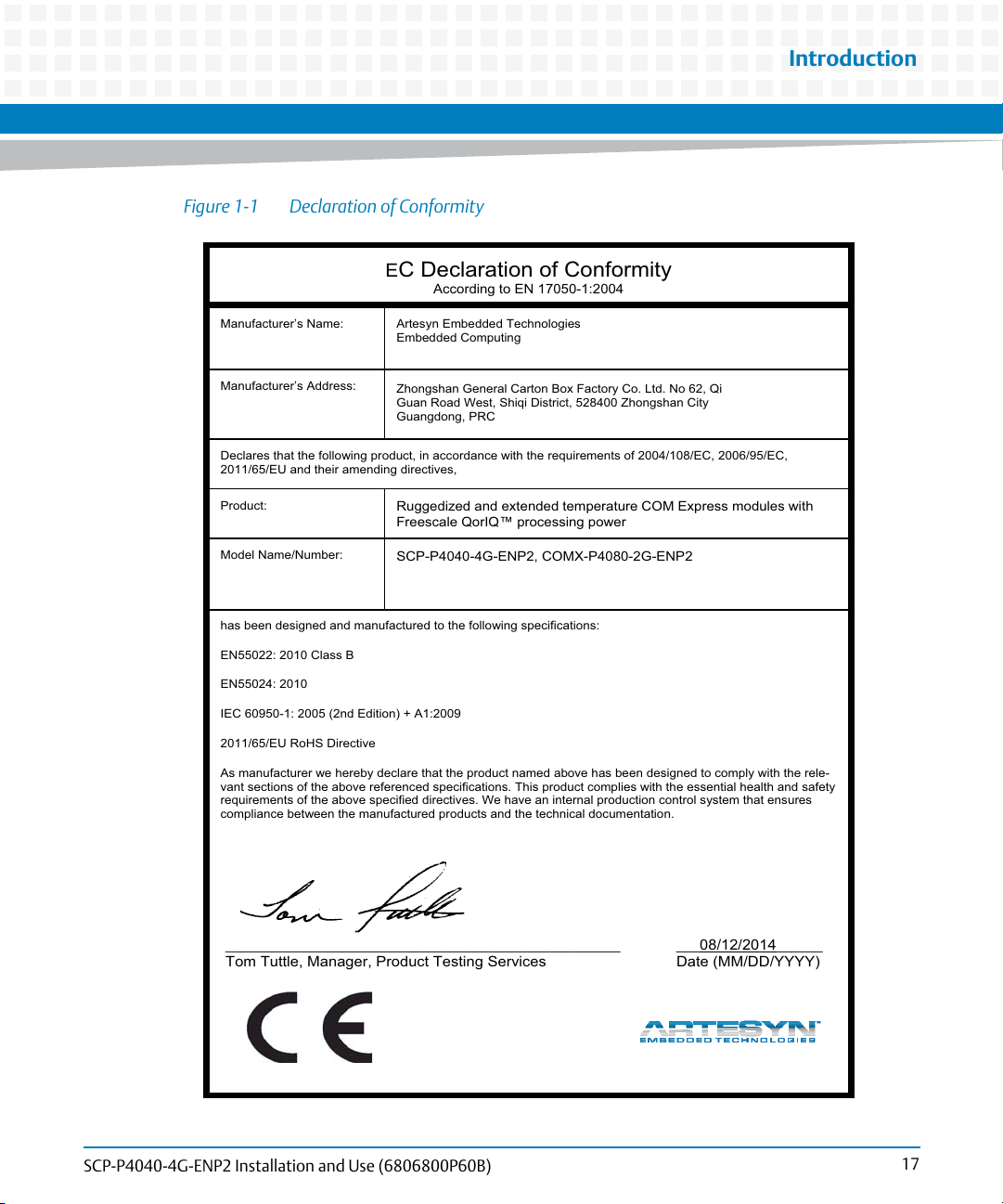
Figure 1-1 Declaration of Conformity
E
C Declaration of Conformity
According to EN 17050-1:2004
Introduction
Manufacturer’s Name:
Manufacturer’s Address:
Declares that the following product, in accordance with the requirements of 2004/108/EC, 2006/95/EC,
2011/65/EU and their amending directives,
Product:
Model Name/Number:
has been designed and manufactured to the following specifications:
EN55022: 2010 Class B
EN55024: 2010
IEC 60950-1: 2005 (2nd Edition) + A1:2009
2011/65/EU RoHS Directive
As manufacturer we hereby declare that the product named above has been designed to comply with the rele-
vant sections of the above referenced specifications. This product complies with the essential health and safety
requirements of the above specified directives. We have an internal production control system that ensures
compliance between the manufactured products and the technical documentation.
Artesyn Embedded Technologies
Embedded Computing
Zhongshan General Carton Box Factory Co. Ltd. No 62, Qi
Guan Road West, Shiqi District, 528400 Zhongshan City
Guangdong, PRC
Ruggedized and extended temperature COM Express modules with
Freescale QorIQ™ processing power
SCP-P4040-4G-ENP2, COMX-P4080-2G-ENP2
___________________________________________________ ___
Tom Tuttle, Manager, Product Testing Services Date (MM/DD/YYYY)
SCP-P4040-4G-ENP2 Installation and Use (6806800P60B)
08/12/2014
______
17
Page 18
Introduction
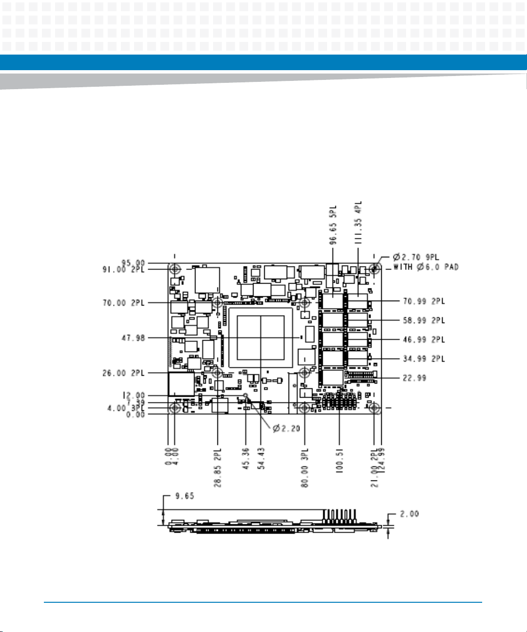
1.3 Mechanical Data
Mechanical Information:
The following figures are the top and bottom view of the board.
Figure 1-2 SCP-P4040-4G-ENP2 Mechanical Dimensions (Top and side views)
18
SCP-P4040-4G-ENP2 Installation and Use (6806800P60B)
Page 19
Table 1-2 PCB Dimensions
Characteristic Value
Height 95 mm
Length 125 mm
Thickness 2 mm
Mounting height top side (component side 1)
Mounting height bottom side (component side 2)
1.4 Ordering Information
Supported Board Models:
As of the printing date of this manual, this guide supports the board models listed in the
following table.
Introduction
Table 1-3 Ordering Information
Order Number Description
SCP-P4040-4G-ENP2 QorIQ P4040 with 4GB memory, ENP2. COM Express Basic size
SCP-P4040-4G-ENP2 Installation and Use (6806800P60B)
19
Page 20
Introduction
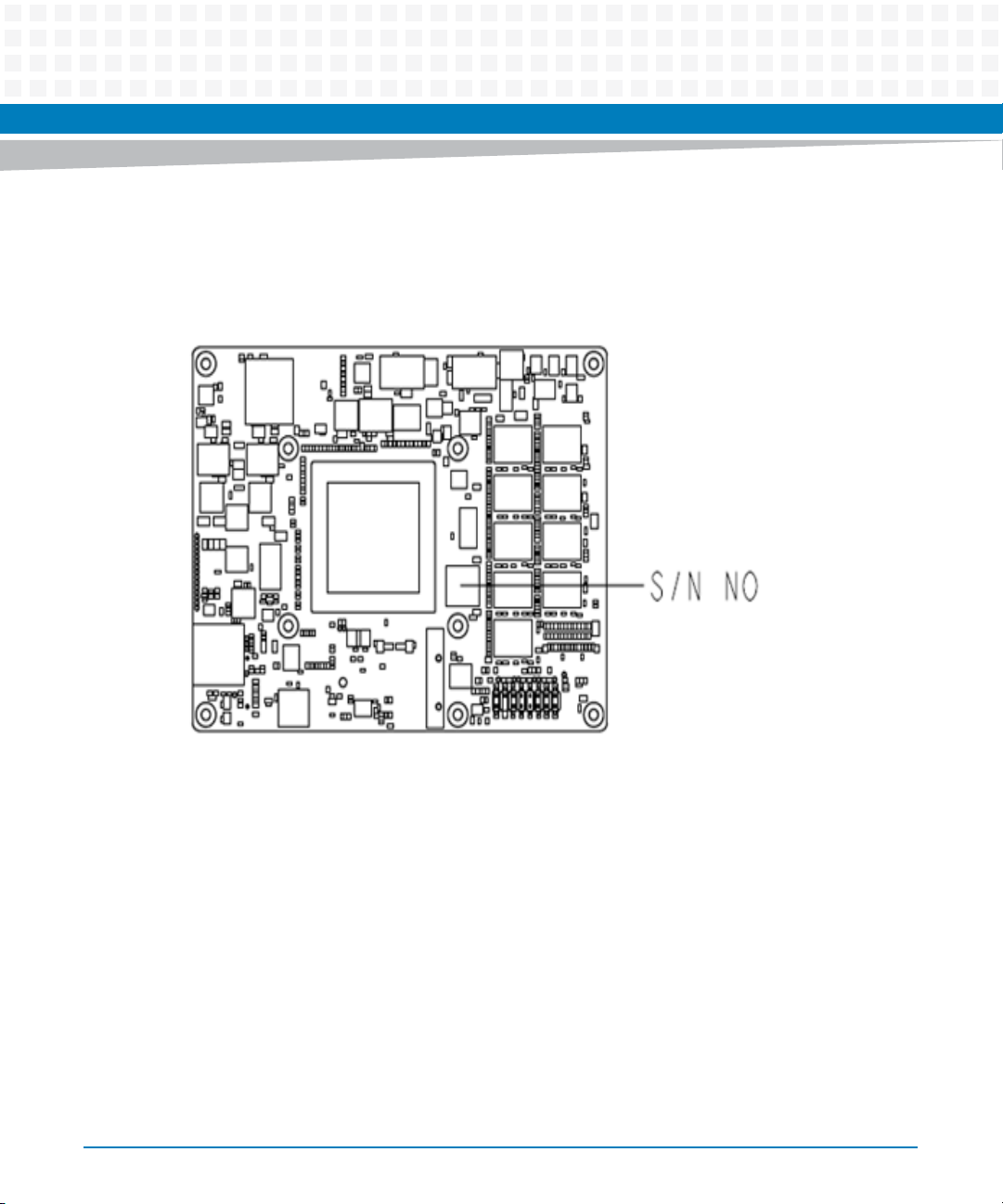
1.5 Production Identification
The following figure shows the location of the board's serial number.
Figure 1-3 Location of Product Serial Number
20
SCP-P4040-4G-ENP2 Installation and Use (6806800P60B)
Page 21
Hardware Preparation and Installation
2.1 Environmental and Power Requirements
You must make sure that following environmental requirements meet when board is operated
in your system configuration.
Operating temperatures refer to the temperature of air circulation around the board,
but not the component temperature.
Environmental Requirements
The following table provides the environmental requirement details for the board.
Chapter 2
Table 2-1 Environmental Requirements
Environmental Factor Operating Non-operating
o
Temperature -40
Humidity to 100% RH to 100% RH
Vibration Random
(1hr/axis)
Shock 30g/11mS(half sine)
Altitude -60 to 4000 m ASL
Vibration Sine
(10mins/axis)
Thermal Requirements
A standard passive heat sink or heat spreader can be provided by Artesyn; 12 CFM system
airflow volume (at 71oC) is needed for the heat sink to keep sufficient cooling to the SCPP4040-4G-ENP2. Contact your Artesyn sales representative for current information on the
detailed thermal information of the SCP-P4040-4G-ENP2.
C to +71oC -50oC to +100
0.04g2/Hz, 15 to 2000Hz
(8GRMS)
5G 15 to 2000Hz
o
C
SCP-P4040-4G-ENP2 Installation and Use (6806800P60B)
21
Page 22
Hardware Preparation and Installation
The following table summarized components that exhibit significant temperature raises and
their maximum allowable operating temperature. These components should be monitored in
order to assess thermal performance during customized thermal solution development.
Table 2-2 Critical Temperature Spots
Component Identifier Heat Dissipation Power (W) Maximum Allowable Temperature (oC)
CPU: P4040 16.8 CPU: 105 (Tj)
GbE Transceiver:
BCM5482
Memory SDRAM: 4GB 3 95 (Tc)
0.86 125 (Tj)
System Overheating
Colling Vents
Improper cooling can lead to system damage and an void the manufacturer's
warranty. To ensure proper cooling and undisturbed airflow through the system do
not obstruct the ventilation openings of the system. Make sure that the fresh air
supply is not mixed with hot exhaust from other devices.
Personal Injury
During operation, hot surfaces may be present on the heat sinks and the components
of the product.
To prevent injury from hot surface, do not touch any of the exposed components or
heatsinks on the product when handling. Use the handle and face plate, where
applicable, or the board edge when removing the product from the enclosure.
22
Power Requirements
SCP-P4040-4G-ENP2 Installation and Use (6806800P60B)
Page 23
Hardware Preparation and Installation
This board is designed to operate with the input voltages and currents as defined in the
following tables.
Table 2-3 Power Requirement (with solder-down memory chips)
State 12v VCC_RCT
Idle 2.81A 100 uA
Full Loading (Linux) 2.91A 100 uA
Table 2-4 Power Dissipation
Item Configuration Power
1 Total power dissipation (W) 34.92
2.2 Unpacking and Inspecting the Board
Damage of Circuits
Electrostatic discharge and incorrect installation and removal of the product can
damage circuits or shorten their life.
Before touching the product make sure that you are working in an ESD-safe
environment or wear and ESD wrist strap or ESD shoes. Hold the product by its
edges and do not touch any components or circuits.
1. Verify that you have received all items of your shipment:
Printed Quick Start Guide and Safety Notes
SCP-P4040-4G-ENP2 Board
Drivers CD
SCP-P4040-4G-ENP2 Installation and Use (6806800P60B)
23
Page 24

Hardware Preparation and Installation
2. Check for damage and report any damage or differences to customer service.
3. Remove the desiccant bag shipped together with the product.
Damage of Circuits
Environmental Damage
Improperly disposing of used products may harm the environment
Always dispose of used products according to your country's legislation and
manufacturer's instructions
2.3 Installing and Removing the Module on the Carrier Board
The heat sink/heat spreader is already assembled with the module before these operations.
Installing the COM module on the carrier board
1. Line up the board-to-board connector of the module assembly with the board-to-board
connector of the carrier board.
2. Make sure that the interconnectors are properly aligned and that the five standoffs on
the module have contact with the top of the carrier board.
3. From the bottom side of the carrier board, locate the screw holes on module and carrier
board.
4. Use the screws to fasten the module to the carrier board.
Removing the COM module from the carrier board
1. From the back side of the carrier, locate the five screws that connect the module assembly
to the carrier board.
24
SCP-P4040-4G-ENP2 Installation and Use (6806800P60B)
Page 25

Hardware Preparation and Installation
2. Loosen and remove the screws.
3. While holding the edges, pull the module from the carrier board.
This installation procedure is only for reference. Assemble the heatsink and the
module based on your own thermal solution.
SCP-P4040-4G-ENP2 Installation and Use (6806800P60B)
25
Page 26

Hardware Preparation and Installation
26
SCP-P4040-4G-ENP2 Installation and Use (6806800P60B)
Page 27

Controls, LEDs, and Connectors
3.1 Connectors and Switches
3.1.1 On-Board Connectors
JTAG Header
The following table lists the pin-out of JTAG connector:
Table 3-1 JTAG connector pin-out
Pin Number Signal Name
1 TDO
2NC
3 TDI
Chapter 3
4TRST
5RUNSTOP
6 VDDSENSE
7 TCK
8 CKSTP INPUT
9TMS
10 NC
11 SRST
12 NC
13 HRST
14 NC
15 CKSTP OUTPUT
16 GND
SCP-P4040-4G-ENP2 Installation and Use (6806800P60B)
27
Page 28

Controls, LEDs, and Connectors
3.2 On Board LEDs
There are several LEDs provided on the module to denote the statements of the system.
The following table lists the LED IDs:
Table 3-2 LED and statements of the system
LED ID Statement of the system
D17 Thermal issue
D18~D19 Debug LED 1~2
D3 System asleep
D7 DDR3 power OK
D4 3.3V power OK
D5 2.5V power OK
D6 1.8V power OK
D13 CORE power OK
D9 PLATFORM power OK
D10 1.5V power OK
D1 USB hub 1 active
D2 USB hub 1 high speed
D15 USB hub 2 active
D16 USB hub 2 high speed
28
SCP-P4040-4G-ENP2 Installation and Use (6806800P60B)
Page 29

Functional Description
The following sections describe the physical and electrical structure of the board in detail.
4.1 Overview
The SCP-P4040-4G-ENP2 is a COM Express module based on the Freescale Power PC P40x0
platform.This board provides some of the universal interfaces such as Gigabit Ethernet, USB,
PCIE, and so on. This board is designed to support the QorIQ P4040 integrated processor
running at the speed of 1.2GHz.
The QorIQ P4040 integrated communication processor combines four Power Architecture™
processor cores with high performance data path acceleration logic, network and peripheral
bus interfaces required for networking, telecommunication, data communication, wireless
infrastructure, and military/aerospace applications.
Chapter 4
SCP-P4040-4G-ENP2 Installation and Use (6806800P60B)
29
Page 30

Functional Description
Freescale
QorIQ
P4040
1.2GHz
COM
Express
Connectors
4.2 Block Diagram
Figure 4-1 SCP-P4040-4G-ENP2 Function Block Diagram
Test Points Aurora x2
Vertical
Debug Header
9xDDR3
2Gbyte
9xDDR3
2Gbyte
JTAG/OOP
Channel 1
1200 Mts
Channel 2
1200
Bank 1 [0 5 ]
SerDes
Block
Bank1 [0 3]
Bank1 [4 7]
Bank2 [10 13]
Bank2 [14 17]
RGMI
RGMI
USB
PHY
Dual
GbE
PHY
256
NOR
Flash
Voltage
Monitor
EE
PROM
PCIex4/SR10x4
PCIex4/SR10x4/4xSGML
PCIex4/4xSGML/XAUI
4/4xSGML/XAUI
USB
HUB
10/100/10000-T
10/100/10000-T
USB
PHY
M001
M002
S010
4XUART
8XGP10
IEEE 1588
Local Bus (1x16)
1GB
NAND
Flash
I2C to
GPIO
I2C
TEMP
Sensor
2
C
I
RTC
I2C
SP1
Reset
Temp Detect
8 x GPO
WDT
4x USB
1XUSBVLP
WDT
V DAT
30
SCP-P4040-4G-ENP2 Installation and Use (6806800P60B)
Page 31

Functional Description
4.3 Processor Core and Cache Memory Complex
The QorIQ P4040 has four high-performance 32-bit Power Architecture Book E-compliant
e500mc cores. Each e500mc is a superscalar dual issue processor that supports out-of-order
execution and in-order completion, thus making it perform better than other RISC and CISC
architectures.
Features of e500mc
36 bit physical addressing
512-entry 4-Kbyte pages
3 Integer units (2 simple, 1 complex)
1.5GHz at 1.0V
64-Byte cache line size
L1 caches
User, Supervisor, and Hypervisor instruction level privileges
APU, classic double precision floating point unit
128-Kb private L2 cache running at the same frequency of CPU
2-Mbyte of shared L3 CoreNet platform cache (CPC)
4.4 Integrated Memory Controller
The P4040 consists of two DDR controllers that support DDR2 and DDR3 SDRAM. It can
support a maximum of 64GByte of main memory. It is capable of ECC, detects and corrects all
single bit errors, double-bit and within a nibble errors. The DDR controller is capable of selfrefresh mode (for compliant DDR SDRAM DIMMs) and an initialization bypass during system
power-on after an abnormal shutdown for use by designers in preventing re-initialization.
SCP-P4040-4G-ENP2 Installation and Use (6806800P60B)
31
Page 32

Functional Description
4.5 Local Bus
The local bus is connected to a 2 Gb or 256 MB NOR Flash and a 08 G bits or 1 G Bytes NAND
flash. The NOR flash is used to store the RCW data, U-boot, and Linux kernel. By default, the
NAND flash is used to store the file system. There are a totally four chip-selectsignals included
in the local bus from CS0 to CS3. Among the CS0 to CS3, only CS0 is enabled during power on
reset. So, the chip-select-signal (CS) of the device connected to local bus from which the
system boots must be connected to CS0.
Local bus with 16 bits data bus (DQ0~DQ15) are directly routed to COM Express connectors.
A “low” state is required to enable local bus output and a “high” state or '1' is required to
disable.
The following figure illustrates the distribution of local bus on P4040:
Figure 4-2 Distribution of local bus on P4040
32
SCP-P4040-4G-ENP2 Installation and Use (6806800P60B)
Page 33

4.5.1 Clock
The eLBC clock is generated by platform clock. The divisor is configured by CLKDIV in Clock
Ratio Register (LCRR). The divisor is 32 when GPCM is selected as RCW source. So the eLBC
clock is platform clock / 32 = 800MHz / 32 = 25MHz.
4.5.2 NOR Flash
The NOR FLASH is attached to the GPCM on local bus and works at 16-bit mode.
The NOR FLASH is Numonyx™ PC28F00 BM29EW H. Its size is 2Gb/ 256MB. It has 2048 uniform
blocks, 128K bytes or 64K words each.
The physical address for NOR FLASH is 0xFE0000000 - 0xFEFFFFFFF.
The NOR FLASH should contain RCW data, u-boot image, u-boot environment variables, kernel
image, device tree blob, RAMDISK image and FMAN ucode image. The detailed map is
described in the following table:N
Functional Description
Table 4-1 NOR Flash Map
Block# Blocks Start End Size Description Static/Variable
0 1 0000 0000 0001 FFFF 128 KB Active RCW
Option Data
1 12 0002 0000 0019 FFFF 1536 KB RCW Option Data Static
13 3 001A 0000 0020 0000 384KB Not Used Static
16 112 0020 0000 00FF FFFF 14 MB FMAN ucode
Image
128 1792 0100 0000 0EFF FFFF 224 MB RAMDISK Image Static
1920 120 0F00 0000 0FEF FFFF 15 MB Kernel Image Static
2040 3 0FF0 0000 0FF5 FFFF 384 KB Device Tree Blob Static
2043 1 0FF6 0000 0FF7 FFFF 128 KB U-Boot Env
Variable
2044 4 0FF8 0000 0FFF FFFF 512 KB U-Boot Image Static
SCP-P4040-4G-ENP2 Installation and Use (6806800P60B)
Static
Static
Static
33
Page 34

Functional Description
4.5.3 NAND Flash
The NAND FLASH is attached to the FCM on local bus and works at 8-bit mode.
The NAND FLASH is Micron MT29F8G08ADADAH4 whose FLASH size is 08 G bits or 1 G Bytes.
The pages are large and each page contains 2112 bytes including 2048 bytes of data and 64
bytes of spare. There are totally 8192 blocks, each block contains 64 pages including 128 KB of
data and 4 KB of spare.
The NAND FLASH is only used as NAND FLASH JFFS2 rootfs.The detailed map is described in the
following table:
Table 4-2 NAND FLASH Map
Start Address End Address Size Description
0000 0000 00FF FFFF 16 MB Not Used
0100 0000 3FFF FFFF 1GB - 16MB NAND FLASH JFFS2 rootfs
4.6 HSSI OR SERDES Block
SCP-P4040-4G-ENP2 contains SERDES 3 banks including a total of 18 lanes. From the 18 lanes
of SERDES, 12 are routed to the COM Express connectors, defined as SERDES0~ SERDES7
(SERDES0~7 of bank 1) and SERDES16~SERDES19 (SERDES10~13 of bank 2).
SERDES8~SERDES9 of bank 1 are used for Aurora debugger defined as Aurora0~1.
The remaining 4 lanes of bank 3 are not used in P4040.
The protocol running at each lane or each group of lanes routed to COM Express connectors are
configured by the RCW, available options are shown in the following table:
Table 4-3 Options of the SERDES routed to COM Express Connectors
Bank1
Option
#
1 PEX1 x4
34
SerDes 0 ~
3 (SLOT J6)
(2.5Gbps)
Bank1 SerDes
4 ~ 7 (SLOT J14)
PEX2 x4
(2.5Gbps)
Bank2 SerDes
10 ~ 13 (SLOT
J10)
XAUI
(3.125Gbps)
SCP-P4040-4G-ENP2 Installation and Use (6806800P60B)
RCW
[SRDS_PRTCL]
0x05 XAUI FM1 10 GEC
Bank 3# SerDes
14~17(slot J2)
Page 35

Functional Description
Table 4-3 Options of the SERDES routed to COM Express Connectors (continued)
Bank1
Option
#
2 PEX1 x4
3 PEX1 x4
4 PEX1 x4
5 PEX1 x4
6 PEX1 x4
7 SRIO2 x4
8 SRIO2 x4
9 SRIO2 x4
10 SRIO2 x4
SerDes 0 ~
3 (SLOT J6)
(2.5Gbps)
(5Gbps)
(5Gbps)
(2.5Gbps)
(5Gbps)
(3.125Gbps)
(3.125Gbps)
(2.5Gbps)
(3.125Gbps)
Bank1 SerDes
4 ~ 7 (SLOT J14)
PEX2 x4
(5Gbps)
PEX2 x4
(2.5Gbps)
PEX2 x4
(5Gbps)
SGMII x 4
(1.25Gbps)
SGMII x 4
(1.25Gbps)
SRIO1 x4
(3.125Gbps)
SRIO1 x4
(3.125Gbps)
SRIO1 x4
(2.5Gbps)
SRIO1 x4
(3.125Gbps)
Bank2 SerDes
10 ~ 13 (SLOT
J10)
XAUI
(3.125Gbps)
XAUI
(3.125Gbps)
XAUI
(3.125Gbps)
XAUI
(3.125Gbps)
XAUI
(3.125Gbps)
PEX3 x4
(2.5Gbps)
PEX3 x4 (5Gbps) 0x19
XAUI
(3.125Gbps)
SGMII x 4
(1.25Gbps)
RCW
[SRDS_PRTCL]
0x05 XAUI FM1 10 GEC
0x05 XAUI FM1 10 GEC
0x05 XAUI FM1 10 GEC
0x0F XAUI FM1 10 GEC
0x0F Reserved
0x19 Reserved
0x13
0x16
Bank 3# SerDes
14~17(slot J2)
2
2
11 PEX1 x4
(2.5Gbps)
12 PEX1 x4
(5Gbps)
SCP-P4040-4G-ENP2 Installation and Use (6806800P60B)
SRIO1 x4
(2.5Gbps)
SRIO1 x4
(2.5Gbps)
XAUI
(3.125Gbps)
XAUI
(3.125Gbps)
0x22
0x22
35
Page 36

Functional Description
The following figure illustrates the distribution of SERDES lanes on P4040:
Figure 4-3 Distribution of SERDES Lanes
36
SCP-P4040-4G-ENP2 Installation and Use (6806800P60B)
Page 37

4.7 Thermal Management
SCP-P4040-4G-ENP2 provides a thermal management strategy.This includes CPU junction
temperature monitoring. The following diagram shows thermal management strategy:
Figure 4-4 Board Thermal Management
Functional Description
A thermal diode is integrated in P40x0, which connects to a thermal sensor ADT7411. The CPU
can get the junction temperature via I2C.
When the junction temperature goes up to105oC, ADT7411 drives INT# to low, indicates an
interrupt to CPU. A red LED D17 can show the interrupt status.
LED Definition Status Description
D17 INT# signal is active ON The CPU temperature
SCP-P4040-4G-ENP2 Installation and Use (6806800P60B)
goes up to 105 ° C
OFF Normal status
37
Page 38

Functional Description
4.8 Main Memory
4.8.1 Memory Interface
QorIQ P40x0 supports two individual DDR channels that may be configured for DDR2 and
DDR3. Each channel consists of 64-bit data and 8 ECC bits. Both unbuffered and registered
memory subsystem schemes are supported.
The module supports 4 GB DDR3 1066MHz ECC memories per channel. 2 GB each channel, one
on top assembly and another at bottom of the PCB. Each channel contains 9x SDRAM chips on
the module.
Total bottom height limit is specified as xx mm while the SDRAM's height is 1.2mm (max).
The memory interface includes all the necessary termination and IO powers.
38
SCP-P4040-4G-ENP2 Installation and Use (6806800P60B)
Page 39

Functional Description
The following figure illustrates the DDR memory architecture per controller:
Figure 4-5 Memory Interface
SCP-P4040-4G-ENP2 Installation and Use (6806800P60B)
39
Page 40

Functional Description
Table 4-4 Memory Capacities
Characteristic Value
Memory technology DDR3
SDRAM chip MT41J256M8HX-15E IT:D
Memory Size 2Gb 256x8
Supply voltage 1.5V
Oracle Number 5106813C55
4.9 Memory Map
The following table provides the memory map of SCP-P4040-4G-ENP2.
Table 4-5 Memory Map
Address# 32-bit Effective
Base Address
1 0000 0000 0 0000 0000 8000 0000 - 2GB DDR3 Memory, NOTE1
2 8000 0000 C 0000 0000 2000 0000 - 512MB PCIE1 MEM
3 A000 0000 C 2000 0000 2000 0000 - 512MB PCIE2 MEM, NOTE2
4 A000 0000 C 2000 0000 1000 0000 - 256MB RIO1 MEM, NOTE2
5 B000 0000 C 3000 0000 1000 0000 - 256MB RIO2 MEM, NOTE2
6 C000 0000 C 4000 0000 0800 0000 - 512MB PCIE3 MEM
7 E000 0000 F E000 0000 1000 0000 - 256MB LBC NOR FLASH
8 F000 0000 F 0000 0000 0040 0000 - 4MB DCSR
9 F400 0000 F F400 0000 0020 0000 - 2MB BMAN MEM
10 F420 0000 F F420 0000 0020 0000 - 2MB QMAN MEM
11 F800 0000 F F800 0000 0001 0000 - 64KB PCIE1 IO
12 F801 0000 F F801 0000 0001 0000 - 64KB PCIE2 IO
13 F802 0000 F F802 0000 0001 0000 - 64KB PCIE3 IO
14 FFA0 0000 F FFA0 0000 0010 0000 - 1MB NAND FLASH Buffer
15 FE00 0000 F FE00 0000 0100 0000 - 16MB CCSR
36-bit Physical
Base Address Size Description
40
SCP-P4040-4G-ENP2 Installation and Use (6806800P60B)
Page 41

Table 4-5 Memory Map (continued)
Functional Description
Address# 32-bit Effective
16 FFFF F000 0 FFFF F000 0000 1000 - 4KB BOOT PAGE
Only upto 2GB memory is mapped in u-boot and the other memory is left unmapped
and not used if more than 2GB memory is fitted. More than 2GB can be used in Linux.
Up to 4GB has been verified.
Address #4 and #5 is used instead of address #3 if RIO is configured.
4.10 GPIO
SCP-P4040-4G-ENP2 consists of totally 21 GPIOs. The following table lists the GPIOs:
Table 4-6 GPIO
GPIO Name Function
Base Address
36-bit Physical
Base Address Size Description
CPU_GPIO0 GPI0 of COME connectors
CPU_GPIO1 GPI1 of COME connectors
CPU_GPIO2 GPI3 of COME connectors
CPU_GPIO3 GPI4 of COME connectors
CPU_GPIO4 GPO0 of COME connectors
CPU_GPIO5 GPO1 of COME connectors
CPU_GPIO6 GPO3 of COME connectors
CPU_GPIO7 GPO4 of COME connectors
CPU_GPIO19 Clock generators enable control
CPU_GPIO20 Carried board reset output
SCP-P4040-4G-ENP2 Installation and Use (6806800P60B)
41
Page 42

Functional Description
Table 4-6 GPIO (continued)
GPIO Name Function
CPU_GPIO23 Clock generator of bank 1 frequency
CPU_GPIO24 Clock generator of bank 2 frequency
CPU_GPIO26 Clock generator of bank 3 frequency
IOEXT_GPI5 GPI5 of COME connectors
IOEXT_GPI6 GPI6 of COME connectors
IOEXT_GPI7 GPI7 of COME connectors
IOEXT_GPI8 GPI8 of COME connectors
IOEXT_GPO5 GPO5 of COME connectors
IOEXT_GPO6 GPO6 of COME connectors
selection
selection
selection
IOEXT_GPO7 GPO7 of COME connectors
IOEXT_GPO8 GPO8 of COME connectors
GPIO18, 19, 20, 23, 24 and 26 are multiplexed with other functional blocks. The pins should be
configured as GPIO in RCW data.
GPIO18/19: RCW [DMA1]=1b
GPIO20: RCW [DMA2]=10b
GPIO23/24/26: RCW [IRQ]=1b
42
SCP-P4040-4G-ENP2 Installation and Use (6806800P60B)
Page 43

Functional Description
After reset, the direction for all GPIOs are set to input. So all the GPIOs used as output needs to
be reconfigured.
Figure 4-6 Distribution of GPIO
SCP-P4040-4G-ENP2 Installation and Use (6806800P60B)
43
Page 44

Functional Description
4.11 SDHC
SCP-P4040-4G-ENP2 provides an SD/MMC interface to the COM Express connector and there
should be a SD card connector provided on the carrier.
This module not only supports SD card but also Micro SD card in which there is no write protect
signal. The sixth bit of the switcher S2 is provided to define whether a SD card or Micro SD card
is embedded in the carrier board.
Table 4-7 SD or Micro SD card on the Carrier
S2.6 Card on the carrier
ON SD card
OFF (Default) Micro SD card
44
SCP-P4040-4G-ENP2 Installation and Use (6806800P60B)
Page 45

4.12 SPI Interface
SCP-P4040-4G-ENP2 provides a SPI bus with 3 chip-select signals. All SPI bus signals are routed
to COM Express connectors.
The following figure illustrates the distribution of SPI bus:
Figure 4-7 Distribution of SPI Bus
Functional Description
4.13 LAN
This module provides 1 GE port with LED controlling signals routing to the COM Express
connectors and the magnetic must be placed on carrier board. The interface used between
MAC and PHY BCM5482 is the RGMII bus in P4040, which is multiplexed with USB1 ULPI bus, so
RCW [EC1] should be set to 00 as RGMII protocol.
U-boot should provide the driver of dTSEC and TCP/IP protocol stack. The U-boot can use TFTP
to download images to memory.
4.13.1 MDIO
There are totally two groups of MDIO buses in P4040. The first group is called EMI1 which
complies with IEEE 802.3 Clause 22. EMI1 has two pins: EMI1_MDC and EMI1_MDIO. It is
available externally only on dTSEC0@FMan1. EMI1 is used for the communication between
dTSEC, MAC, and PHY. SGMII PHY is also managed by EMI1.
The second group is called EMI2 which complies with IEEE 802.3ae Clause 45. EMI2 has two
pins: EMI2_MDC and EMI2_MDIO. It is available externally only on 10GEC of FMan1. EMI2
is used for the communication between 10GEC and PHY.
SCP-P4040-4G-ENP2 Installation and Use (6806800P60B)
45
Page 46

Functional Description
4.13.2 PHY
dTSEC0@FMan1 is connected to BCM5482 via RGMII. There are totally two ports included in
the GE PHY BCM5482 and only first port is used.The MDIO address for the first port is 0x01 and
the second is 0x02.
The MDIO addresses for 4 SGMII PHYs are 0x1C, 0x1D, 0x1E and 0x1F when SerDes option
#5/#6 or #10 is applied.
4.14 UART Interface
SCP-P4040-4G-ENP2 consists of 4 UARTS (Tx and Rx signals for each UART) or 2 DUARTS (Tx,
Rx, CTS, RTS signals for each DUART) that are routed to the COM Express connectors. Several
optional resistors are provided to determine whether UARTS or DUARTS are routed.
When UARTS are routed, R383, R385, R387, and R389 are installed and R382, R384, R386, and
R388 are removed, and vice versa.
UART option is the default setting.
4.15 RTC & WDT
The RTC and WDT functions provided in the module are embedded separated in 2 ICs, U2100
and U2101 respectively. The WDT is accessed through I2C1 bus of the processor, and the RTC
is accessed through I2C2 bus, both with an address of 0xD0.The WDT triggers a reset output
signal for power-on reset, and the RTC provides a 32 KHz clock output for the RTC clock input
of the processor. Battery backup for the RTC is supplied by the VCC_BAT pin on the COME
connectors.
Table 4-8 Real Time Clock
Characteristic Value
Vendor ST Micro
46
SCP-P4040-4G-ENP2 Installation and Use (6806800P60B)
Page 47

Table 4-8 Real Time Clock (continued)
Characteristic Value
Device M41T62LC6F
Function Real-time clock with
alarm interrupt,
programmable square
wave output
Package LCC8 (1.5 mm x 3.2 mm)
Oracle Number 5106837C55
Table 4-9 WDT
Characteristic Value
Vendor ST Micro
Device M41T65Q6F
Functional Description
Function Watchdog output
Package QFN16 (3 mm x 3 mm)
Oracle Number 5106837C56
4.16 USB
This module consists of one USB PHY (USB3315) and one 4-ports (USB4~USB7) USB hub
(USB2514). The interface between the USB controller and USB PHY is ULPI bus, the second
group of multiplexing interface RGMII/ULPI. So the RCW should be properly set for the using of
the second group of ULPI bus.
The operating mode of the USB hub is configured by hardware strapping, and it can also be
configured by I2C bus by changing the state of the strapping pins. Hardware strapping is the
default method. The I2C bus address of the USB hub is 0x58 when configured.
SCP-P4040-4G-ENP2 Installation and Use (6806800P60B)
47
Page 48

Functional Description
By default configuration, all 4 USB ports of the hub are removable and all indicating signals are
active high. Two LED provided on the module to indicate the operating state of the USB hub.
One is hub active indicating LED and the other is hub high speed indicating LED.
Table 4-10 USB PHY
Characteristic Value
Vendor SMSC
Device USB3315C-CP-TR
Function USB Transceiver (PHY)
Package QFN24 (4.0mm x 4.0mm x 1.0mm)
Oracle Number 5106812C21
Table 4-11 USB HUB
Characteristic Value
Vendor SMSC
Device USB2514Bi-AEZG
Function USB Hub Controller
Package QFN36 (6.0mm x 6.0mm x 1.0mm)
Oracle Number 5106812C33
4.16.1 Four USB Ports
All four USB interfaces are directly connected to the COM Express connector.
All the four USB ports signals with two over current detecting signals, USB_OC_0_1_N and
USB_OC_2_3_N are routed to the COM Express connectors. USB_OC_0_1_N is for USB0 and
USB1, USB_OC_2_3_N is for USB2 and USB3.
4.17 I2C Interface
The Freescale Power PC P4040 consists of four I2C buses. Among four I2C buses, the I2C3 bus
is multiplexed with SDHC bus and remaining I2C buses are routed to COM Express connectors.
48
SCP-P4040-4G-ENP2 Installation and Use (6806800P60B)
Page 49

Functional Description
There is only one device attached to the second I2C bus I2C2, and there are 6 devices attached
o the first I2C bus I2C1.
The following figure illustrates the distribution of the I2C buses:
Figure 4-8 Distribution of I2C buses
SCP-P4040-4G-ENP2 Installation and Use (6806800P60B)
49
Page 50

Functional Description
Table 4-12 I2C Interface
Address Bus Component Function Oracle Number
0xDC I2C1 9FG104DGILFT Clock Generator 51NL9655W46
0xD0 I2C1 M41T65Q6F Watchdog 5106837C56
0x30 I2C1 PCA9557PW-T IO-Expander 51NL9637V06
0xAC I2C1 MCP98243T-BE/ST SPD Channel A 5106819C29
0xA4 I2C1 MCP98243T-BE/ST SPD Channel B 5106819C29
0x90 I2C1 ADT7411ARQZ-
REEL7
0xAE I2C1 AT24C02-SSHM-T
AT24C512C-SSHM-T
0xA8 I2C1 AT24C512C-XHM-T Processor ID EEPROM 5106813D81
0xD0 I2C2 M41T62LC6F RTC 5106837C55
4.17.1 I2C Device EEPROM
The ADT7411 thermal sensor is a dual-channel digital thermometer and under/over
temperature alarm. It is used in computers and thermal management systems. The ADT7411
thermal sensor is located on I2C1, U2900. The device address is 0x90. It is designed for
monitoring P4040 processor temperature.
The ADT7411 can accurately measure the temperature of a remote thermal diode to ±1°C and
the ambient temperature to ±3°C. The temperature measurement range defaults to 0°C to
+127°C, but can be switched to a wider measurement range of-55°C to +150°C. The ADT7411
communicates over a 2-wire serial interface compatible with system management bus
(SMBus) standards. An ALERT output signals when on-chip or remote temperature is out of
range. The THERM output is a comparator output that allows on/off control of a cooling fan.
The ALERT output can be reconfigured as a second THERM output, if required.
Voltage Monitor/ Temp
Sense
2kb Boot Config
EEPROM 512kb Boot
Config EEPROM
227975
5106813C77
5106813D51
50
By default, u-boot should mask THERM and ALERT output, set the temperature measurement
range from 0°C to +127°C. For setting operation mode and fetching the monitoring
temperature, u-boot should provide u-boot commands.
SCP-P4040-4G-ENP2 Installation and Use (6806800P60B)
Page 51

4.17.2 I2C Device EEPROM
I2C device consists of two I2C EEPROMs, AT24C02C and AT24C512C. These EEPROMs are
located on I2C1; one is for ID EEPROM (U30, AT24C02C, storing board serial number, MAC
address and so on.) and the other is for Processor EEPROM (U2001, AT24C512C, storing
processor ID and so on). The I2C addresses of these EEPROMs are 0xAE and 0xA8.
The EEPROM provides 2048 bits of serial electrically erasable and programmable read-only
memory (EEPROM) organized as 256 words of 8 bits each.
AT24C02 support SEQUENTIAL READ and page write.
Sequential reads are initiated by either a current address read or a random address read. After
micro-controller receives a data word, it responds with an acknowledge. As long as the
EEPROM receives an acknowledge, it will continue to increment the data word address and
serially clock out sequential data words. When the memory address limit is reached, the data
word address will roll over and the sequential read will continue.
Functional Description
AT24C02's 32K EEPROM was internally organized with 32 pages of 8 bytes each. A page write is
initiated the same as a byte write, but the micro-controller does not send a stop condition after
the first data word is clocked in. Instead, after the EEPROM acknowledges receipt of the first
data word, the micro-controller can transmit up to seven more data words.
4.17.3 I2C Device WDT
The WDT M41T65Q is located on I2C1, U2101 and the device address is 0xD0.
U-boot has the following considerations:
By default, u-boot should mask event output and disable WDT.
U-boot should provide commands for enabling WDT and disabling WDT.
4.17.4 I2C Device RTC
The RTC M41S62L is located on I2C2, U2100 and the device address is 0xD0.
SCP-P4040-4G-ENP2 Installation and Use (6806800P60B)
51
Page 52

Functional Description
U-boot has the following considerations:
U-boot should provide commands for setting RTC date/time and getting RTC date/time.
4.17.5 I2C Device Clock Generator
The clock generator ICS9FG104 is located on I2C1, U17 and the device address is 0xDC.
The ICS9FG104 is a Frequency Timing Generator that provides four differential output pairs
that are compliant to the Intel CK410 specification. It also provides support for PCI-Express and
SATA. The part synthesizes several output frequencies from either a 14.31818 MHz crystal or a
25 MHz crystal. The device can also be driven by a reference clock input instead of a crystal. It
provides outputs with cycle-to-cycle jitter of less than 50 ps and output-to-output skew of less
than 35 ps. The ICS9FG104 also provides a copy of the reference clock.
Frequency selection can be accomplished via strap pins or SMBus control. By default, strap pins
work.
For SCP-P4040-4G-ENP2, the input clock for ICS9FG104 is 25 MHz and three differential output
pairs are provided. First pair are connected to SerDes Bank 1, second pair are connected to x2
Aurora Connector, and third pair are connected to COM Express connector. The forth output
pairs are not connected.
When using strap pins to select output frequency, SEL14M_25M# (FS3) is attached to ground
(0) by option resistor. FS2 and FS1 have internal 120K pull down and the option resistors should
not be soldered. FS0 is controlled by GPIO23 and S1.2. When FS0 is 0 (low level), 100MHz clock
output is selected and When FS0 is 1 (high level), 125MHz clock output is selected.
4.17.6 I2C Device USB
I2C device consists of one USB2514 located on I2C2, U25 and the device address is 0x58.
USB2514 is a USB hub controller IC with four downstream ports for embedded USB solutions.
The 4-port hub is fully compliant with the USB 2.0 Specification and will attach to an upstream
port as a Full-Speed Hub or as a Full-/High-Speed Hub, and High Speed (if operating as a HighSpeed Hub) downstream devices on all of the enabled downstream ports.
52
SCP-P4040-4G-ENP2 Installation and Use (6806800P60B)
Page 53

Functional Description
The SMSC Hub must be configured in order to correctly function when attached to a USB host
controller. There are three principal ways to configure the hub: SMBus, EEPROM, or by internal
default setting. In all cases, the configuration method will be determined by the CFG_SEL2,
CFG_SEL1 and CFG_SEL0 pins immediately after RESET_N negation.
In SMBus case, the CFG_SEL1 and CFG_SEL0 pins must be 01, so that Hub can be configured as
an SMBus slave for external download of user-defined descriptors.
U-boot should initialize USB hub during boot-up and provide u-boot commands for
reading/writing the hub's registers.
SCP-P4040-4G-ENP2 Installation and Use (6806800P60B)
53
Page 54

Functional Description
54
SCP-P4040-4G-ENP2 Installation and Use (6806800P60B)
Page 55

Clock Structure
The SCP-P4040-4G-ENP2 needs several kinds of single ended and differential clocks for
booting up and normal operating. Following is the clock distribution tree:
Figure 5-1 Clock Distribution
Chapter 5
Crystal
Crystal
ICS9FG104
(<50ps)
ICS9FG104
(<50ps)
Reference clock for
Bank 1#
100 MHz
100 MHz
125 MHz
125 MHz
Device on
Carrier
Crystal
Device on
Carrier
GE PHY
Bank 1 Bank 2 Bank 3
P4040
COME Connector
Reference clock for
Bank 2#/3#
100 MHz
32.768 KHz
60 MHz
100 MHz
OSC
RTC
32.768
KHz
USB PHY
USB PHY
24 MHz
CY2305
24 MHz
OSC
SCP-P4040-4G-ENP2 Installation and Use (6806800P60B)
55
Page 56

Clock Structure
For ruggedized variant where dip switches are not mounted, the following signals connects to
COM Express connector and will be up to carrier to configure them:
SERDES bank 1
reference clock select
(pin B97 on COME)
Bank1_SEL_FS0=0,
100MHz
Bank1_SEL_FS0=1,
125MHz
*Default:100MHz *Default:125MHz *Default:125MHz
SERDES bank 2
reference clock select
(pin B98 on COME)
Bank2_SEL_S1=0,
100MHz
Bank2_SEL_S1=1,
125MHz
SERDES bank 3
reference clock select
(pin B99 on COME)
Bank2_SEL_S1=0,
100MHz
Bank2_SEL_S1=1,
125MHz
For standard commercial variant where dip switches are populated, the frequency of all the
three SERDES banks' reference clock is selectable between 100MHz and 125MHz by three bits
of switcher S1.
SERDES bank 1
reference clock
Default:100MHz Default:125MHz Default:125MHz
SERDES bank 2
reference clock
SERDES bank 3
reference clock
It can also be set by three GPIOs, referring to the following table:
Table 5-1 Configuration of the frequency of SERDES reference clock by GPIO
SERDES bank 1 reference
clock SERDES bank 2 reference clock SERDES bank 3 reference clock
56
CPU_GPIO23=0, 100MHz CPU_GPIO24=0, 100MHz CPU_GPIO26=0, 100MHz
CPU_GPIO23=1, 125MHz CPU_GPIO24=1, 125MHz CPU_GPIO26=1, 125MHz
Default:100MHz Default:125MHz Default:125MHz
The setting of these three bits of S1 or GPIOs depends on the protocols running at the SERDES
lanes of each bank. When the SERDES lanes are running at the speed of 3.125 Gbps, then the
corresponding bank reference clock should be set as 125 MHz, and at the speed besides 3.125
Gbps, it should be set as 100 MHz. For example, if lanes in bank 1 are configured as PCIE, then
the bank 1 reference clock should be set as 100 MHz, and if XAUI, then should be set as 125
MHz.
SCP-P4040-4G-ENP2 Installation and Use (6806800P60B)
Page 57

On-Boards Power Domains
This subsection describes the power supply system for the module. Power is supplied to
module from ATX-type (using Artesyn carrier) power supply through COME connectors and
on-board regulators supply required voltages to devices on the module.
Figure 6-1 Power Tree
Chapter 6
SCP-P4040-4G-ENP2 Installation and Use (6806800P60B)
57
Page 58

On-Boards Power Domains
6.1 Power Controlling Sequence
The power sequencing of SCP-P4040-4G-ENP2 differs between secure boot mode and non
secure boot mode. For secure boot mode, POVDD should be set to 1.5V DC and is powered at
least 100 system clock cycles after the rising edge of power on reset signal. For non-secure
boot mode, POVDD should be set to GND.
Figure 6-2 Power Sequence of SCP-P4040-4G-ENP2
58
SCP-P4040-4G-ENP2 Installation and Use (6806800P60B)
Page 59

BSP
7.1 BSP Build Requirements
Build Host
The Basic Support Package (BSP) is hosted by an x86 computer running Linux. At least 1 GB free
space is required where the BSP is hosted.
Build Tools
Artesyn is using build tools provided in Freescale SDK1.0 QorIQ-DPAA-SDK-20110609systembuilder.iso to build BSP images for SCP-P4040-4G-ENP2.
You can download the Freescale SDK ISO files from and install it on the build host
Chapter 7
7.1.1 Install Build Tools of SDK1.0
Following are the steps to install build tools of SDK1.0 from Freescale SDK on host computer:
1. Login to the Linux host as a non-root user, <user_name>.
2. Copy the QorIQ-DPAA-SDK-20110609-systembuilder.iso file to this Linux host.
3. Run the ISO file using the following command:
sudo mount -o loop QorIQ-DPAA-SDK-20110609-systembuilder.iso
/mnt/
4. Create a /opt/freescale directory and update access privileges using the following
command
sudo mkdir -p /unixopt/sdk1.0
sudo chmod a+rwx /unixopt/sdk1.0
5. Change directory to mount using the following command:
cd /mnt/
6. Install the Freescale LTIB using the following commands:.
/install
SCP-P4040-4G-ENP2 Installation and Use (6806800P60B)
59
Page 60

BSP
<Input /unixopt/sdk1.0 as the installation target directory>
Do not interrupt the installation process.
7. Execute the cd /unixopt/sdk1.0/QorIQ-DPAA-SDK-20110609-system builder
command.
8. Create a PDK project for P4040DS using the following command:
./scripts/create-config.py --config-file=fsl-p4040ds/samplecreate-config.ini
9. Setup cross-compile environment using the source build_p4040ds_release/bitbake.rc
command.
10. Build Freescale P4040DS BSP images for building test using the bitbake devel-image
command:
7.2 BSP Source Code Package
7.2.1 De-Compose Source Code Package
Copy the SCP-P4040-4G-ENP2 released BSP source code package
COMX_P4040_SRC_<Version Number>.tar.gz to the build host and un-compress it in
current directory:
tar xzvf COMX_P4040_SRC_<Version Number>.tar.gz
There will be a newly-created folder named p4040 which contains SCP-P4040-4G-ENP2 source
code.
Table 7-1 BSP Source Code Package Layout
File/Directory Name Description
build.sh Top script for building all of BSP images for BSP release. It calls Makefile
to perform the operations.
60
SCP-P4040-4G-ENP2 Installation and Use (6806800P60B)
Page 61

Table 7-1 BSP Source Code Package Layout (continued)
File/Directory Name Description
clean.sh Top script for cleaning all of BSP images and temporary objects for BSP
release. It calls Makefile to perform the operations.
linux/ linux/ directory contains Linux kernel, rootfs and rootfs building scripts.
Makefile Top makefile for building/cleaning all of BSP images for BSP release. It
calls Makefiles and scripts located in sub-directories to perform the
operations.
Makefile-p4040ds Top makefile for building/cleaning all of BSP images for P4040DS BSP
release. It calls Makefiles and scripts located in sub-directories to
perform the operations.
misc/ misc/ contains FMAN uCode and RCW.
u-boot/ U-Boot source code.
BSP
7.2.2 Setup Build Environment
If Freescale SDK1.0 is used as build tool, and the host linux is 32 bit, modify the Makefile
and set the environment variant PPC_TOOL_PATH as below:
SDK_INSTALL_PATH ?= /unixopt/sdk1.0/QorIQ-DPAA-SDK-20110609systembuilder
PPC_TOOL_PATH ?= $(SDK_INSTALL_PATH)/freescale-
2010.09/bin:$(SDK_INSTALL_PATH)/build_p4040ds_release/sysroots/
i686-linux/usr/bin
The build tool is not verified with SDK1.0 at 64bit Linux host.
7.3 Build BSP Images
Output Directory
SCP-P4040-4G-ENP2 Installation and Use (6806800P60B)
61
Page 62

BSP
By default, the output directory for building BSP images is /local/tmp/.You need to create this
directory and provide full privileges for all users to access. Use the following commands to
create directory and provide privileges:
sudo mkdir -p
sudo chmod a+rwx /local/ /local/tmp/
Build a Release
To build a release, run the./build.sh <Version_Number> command.
The version number is formatted as VxxxAxx, VxxxBxx, VxxxTxx or VxxxRxx.
For example: V100B00.
BSP Images
SCP-P4040-4G-ENP2 BSP images should be placed in /local/tmp/. It includes the
COMX_P4040_<Version_Number>.tar.gz package:
The COMX_P4040_<Version_Number>.tar.gz package contains:
comx.dtb: Device Tree Blob
fsl_fman_ucode_P3_P4_P5_101_8.bin: FMAN uCode
rcw.bin: RCW
rcw-codewarrior.bin: RCW used for codewarrior to burn image to NOR Flash
rootfs_ext2.img: RAMDISK image
rootfs_nfs.tar.gz: NFS rootfs
u-boot.bin (U-Boot)
uImage: Linux kernel image
62
SCP-P4040-4G-ENP2 Installation and Use (6806800P60B)
Page 63

7.3.1 Build U-Boot
The U-Boot is based on SDK1.0 whose version is U-Boot 2011.06-rc2.
Commands
1. Build by default
make uboot
2. Build Targets supported for UBoot
uboot: configures and builds u-boot.bin for NOR flash
uboot -clean: cleans the u-boot
Output
The built image is u-boot.bin in the current working directory.
BSP
7.3.2 Build Linux Kernel
The Linux kernel is based on SDK1.0 whose version is 2.6.34.6.
Command
1. Build by default
make kernel dtb
2. Build Targets supported for Linux kernel
config-default: copies the SCP-P4040 default configuration to current
configuration
kernel-config: configures the kernel based on current configuration
kernel: compiles kernel with current configuration
kernel-clean: cleans the kernel
dtb: compiles device tree binary
Output
The build images are uImage and comx.dtb in the current working directory.
SCP-P4040-4G-ENP2 Installation and Use (6806800P60B)
63
Page 64

BSP
7.3.3 Build ROOTFS
The rootfs for SCP-P4040-4G-ENP2 include RAMDISK and NFS.
Commands
1. make rootfs: The output image is/local/tmp/<username>/rootfs_ext2.img
2. Build Targets supported for rootfs
rootfs: builds rootfs
rootfs-ext2: builds rootfs for ram disk
rootfs-nfs: builds rootfs for nfs
rootfs-clean: clean the rootfs
Output
The build images are rootfs_ext2.img and rootfs_nfs.tar.gz in the current
working directory.
7.3.4 Build Misc Firmware
Misc Firmware for SCP-P4040-4G-ENP2 includes FMAN uCode and RCW image:
FMAN uCode is misc/fman_ucode/fsl_fman_ucode_P3_P4_P5_101_8.bin
RCW image is misc/rcw/rcw.bin
Both images are binary files and need not to re-build. They are copied to release package
while building.
7.4 DEPLOY BSP IMAGES
This section explains how to deploy BSP images. Assuming that you have built a BSP release
64
SCP-P4040-4G-ENP2 Installation and Use (6806800P60B)
Page 65

package COMX_P4040_V100B00.tar.gz by running ./build.sh V100B00 located at
/local/ tmp/.
7.4.1 Pre-Deployment Steps
The following steps must be performed before deployment:
1. Connect the board to your network using a network cable to the SGMII Ethernet port.
2. Setup a TFTP server in this network. Assuming that the IP address of this server is
192.168.0.100 and the root directory is /tftpboot/.
3. Create a comx_p4040/ in /tftpboot/ subdirectory.
4. Copy the COMX_P4040_<Version_Number>.tar.gz file into the directory
/tftpboot/comx_p4040/ on TFTP server.
5. Change current directory to /tftpboot/comx_p4040/.
BSP
6. Unzip the.tar.gz file to the current directory. The following files are extracted to
theCOMX_P4040_V100B00/:
comx.dtb
rcw.bin
rcw-codewarrior.bin
rootfs_ext2.img
rootfs_nfs.tar.gz
uImage
fsl_fman_ucode_P3_P4_P5_101_8.bin
u-boot.bin
7. Unzip the rootfs_nfs.tar.gz file to the /tftpboot/comx_p4040/ location using
the sudo tar xzvf COMX_P4040_V100B00/rootfs_nfs.tar.gz.
8. Add /tftpboot/comx_p4040/rootfs_nfs/ to NFS exports list in
/etc/exports:/tftpboot/comx_p4040/rootfs_nfs
*(rw,sync,no_root_squash)
9. Restart NFS service to export /tftpboot/comx_p4040/rootfs_nfs/ using the
sudo/sbin/service nfs restart command.
SCP-P4040-4G-ENP2 Installation and Use (6806800P60B)
65
Page 66

BSP
10. The following commands should be executed in U-boot command line.
11. Setup the U-Boot environment variables for the network settings. Example:
=> setenv ethaddr 00:01:af:12:23:01
=> setenv ipaddr 192.168.0.99
=> setenv netmask 255.255.255.0
=> setenv gatewayip 192.168.0.1
=> setenv serverip 192.168.0.100
=> setenv ethact FM1@DTSEC1
12. Setup the U-Boot environment variables for upgrade files. Example:
=> setenv rcwfile comx_p4040/COMX_P4040_V100B00/rcw.bin
=> setenv fmanfile
comx_p4040/COMX_P4040_V100B00/fsl_fman_ucode_P3_P4_P5_101_8.bin
=> setenv bootfile comx_p4040/COMX_P4040_V100B00/uImage
=> setenv norfsfile
comx_p4040/COMX_P4040_V100B00/rootfs_ext2.img
=> setenv fdtfile comx_p4040/COMX_P4040_V100B00/comx.dtb
=> setenv ubootfile comx_p4040/COMX_P4040_V100B00/u-boot.bin
=> setenv rootpath /tftpboot/comx_p4040/rootfs_nfs
13. Test that the network and filename settings can download the files successfully. Example:
=> tftpboot $loadaddr $rcwfile
=> tftpboot $loadaddr $fmanfile
=> tftpboot $loadaddr $bootfile
=> tftpboot $loadaddr $norfsfile
=> tftpboot $loadaddr $fdtfile
=> tftpboot $loadaddr $ubootfile
7.4.2 Deploying BSP Images on NOR FLASH
Following are the steps to delpoy BSP images on NOR FLASH:
1. Upgrade RCW, FMAN uCode, kernel, RAMDISK image, U-Boot and DTB on NOR FLASH
individually. Example:
=> run updrcw; run updfman; run updkernel; run updnorfs; run
updfdt; run upduboot
2. Erase previous U-Boot environment settings using the => run eraenv command.
3. Reset the board using the => reset command. The board will boot up with new BSP.
66
SCP-P4040-4G-ENP2 Installation and Use (6806800P60B)
Page 67

7.5 RAMBOOT
Run run ramboot in U-Boot. ramboot will load RAMDISK, Linux kernel and DTB into RAM via
network by TFTP and then boot.
7.6 NORBOOT
Run run norboot in U-Boot. norboot will load RAMDISK, Linux kernel and DTB from NOR
FLASH into RAM and then boot. For details, please refer to SCP-P4040-4G-ENP2 User Manual.
7.7 NFSBOOT
Run run nfsboot in U-Boot. nfsboot will load Linux kernel and DTB into RAM via network by
TFTP and then boot. And then mounting NFS on remote server as rootfs. For details, please
refer to SCP-P4040-4G-ENP2 User Manual.
BSP
SCP-P4040-4G-ENP2 Installation and Use (6806800P60B)
67
Page 68

BSP
68
SCP-P4040-4G-ENP2 Installation and Use (6806800P60B)
Page 69

Safety Notes
This section provides warnings that precede potentially dangerous procedures throughout
this manual. Instructions contained in the warnings must be followed during all phases of
operation, service, and repair of this equipment. You should also employ all other safety
precautions necessary for the operation of the equipment in your operating environment.
Failure to comply with these precautions or with specific warnings elsewhere in this manual
could result in personal injury or damage to the equipment.
Artesyn intends to provide all necessary information to install and handle the product in this
manual. Because of the complexity of this product and its various uses, we do not guarantee
that the given information is complete. If you need additional information, ask your Artesyn
representative.
The product has been designed to meet the standard industrial safety requirements. It must
not be used except in its specific area of office telecommunication industry and industrial
control.
Only personnel trained by Artesyn or persons qualified in electronics or electrical engineering
are authorized to install, remove or maintain the product.
The information given in this manual is meant to complete the knowledge of a specialist and
must not be used as replacement for qualified personnel.
Keep away from live circuits inside the equipment. Operating personnel must not remove
equipment covers. Only Factory Authorized Service Personnel or other qualified service
personnel may remove equipment covers for internal subassembly or component replacement
or any internal adjustment.
Do not install substitute parts or perform any unauthorized modification of the equipment or
the warranty may be voided. Contact your local Artesyn representative for service and repair
to make sure that all safety features are maintained.
SCP-P4040-4G-ENP2 Installation and Use (6806800P60B)
69
Page 70

Safety Notes
70
SCP-P4040-4G-ENP2 Installation and Use (6806800P60B)
Page 71

Sicherheitshinweise
Dieses Kapitel enthält Hinweise, die potentiell gefährlichen Prozeduren innerhalb dieses
Handbuchs vorrangestellt sind. Beachten Sie unbedingt in allen Phasen des Betriebs, der
Wartung und der Reparatur des Systems die Anweisungen, die diesen Hinweisen enthalten
sind. Sie sollten außerdem alle anderen Vorsichtsmaßnahmen treffen, die für den Betrieb des
Produktes innerhalb Ihrer Betriebsumgebung notwendig sind. Wenn Sie diese
Vorsichtsmaßnahmen oder Sicherheitshinweise, die an anderer Stelle diese Handbuchs
enthalten sind, nicht beachten, kann das Verletzungen oder Schäden am Produkt zur Folge
haben.
Artesyn ist darauf bedacht, alle notwendigen Informationen zum Einbau und zum Umgang mit
dem Produkt in diesem Handbuch bereit zu stellen. Da es sich jedoch um ein komplexes
Produkt mit vielfältigen Einsatzmöglichkeiten handelt, können wir die Vollständigkeit der im
Handbuch enthaltenen Informationen nicht garantieren. Falls Sie weitere Informationen
benötigen sollten, wenden Sie sich bitte an die für Sie zuständige Geschäftsstelle von Artesyn.
Das System erfüllt die für die Industrie geforderten Sicherheitsvorschriften und darf
ausschließlich für Anwendungen in der Telekommunikationsindustrie und im Zusammenhang
mit Industriesteuerungen verwendet werden.
Einbau, Wartung und Betrieb dürfen nur von durch Artesyn ausgebildetem oder im Bereich
Elektronik oder Elektrotechnik qualifiziertem Personal durchgeführt werden. Die in diesem
Handbuch enthaltenen Informationen dienen ausschließlich dazu, das Wissen von
Fachpersonal zu ergänzen, können dieses jedoch nicht ersetzen.
Halten Sie sich von stromführenden Leitungen innerhalb des Produktes fern. Entfernen Sie auf
keinen Fall Abdeckungen am Produkt. Nur werksseitig zugelassenes Wartungspersonal oder
anderweitig qualifiziertes Wartungspersonal darf Abdeckungen entfernen, um Komponenten
zu ersetzen oder andere Anpassungen vorzunehmen.
Installieren Sie keine Ersatzteile oder führen Sie keine unerlaubten eränderungen am Produkt
durch, sonst verfällt die Garantie. Wenden Sie sich für Wartung oder Reparatur bitte an die für
Sie zuständige Geschäftsstelle von Artesyn. So stellen Sie sicher, dass alle
sicherheitsrelevanten Aspekte beachtet werden.
SCP-P4040-4G-ENP2 Installation and Use (6806800P60B)
71
Page 72

Sicherheitshinweise
72
SCP-P4040-4G-ENP2 Installation and Use (6806800P60B)
Page 73

Page 74

Artesyn Embedded Technologies, Artesyn and the Artesyn Embedded Technologies logo are trademarks and service marks of Artesyn Embedded Technologies, Inc.
All other product or service names are the property of their respective owners.
©
2014 Artesyn Embedded Technologies, Inc.
 Loading...