

APC558
Dual Operational Amplifier
Features
••
• Power Supply Range :
••
• Signal Supply : 3V to 20V
• Dual Supply : ± 1.5V to ± 10V
••
• Large DC Voltage Gain : 100dB
••
••
• Large Output Swing : 0V ~ V
••
••
• Bandwidth(unity gain) : 2MHz
••
••
• Internally Frequency Compensated for Unity
••
Gain
••
• Low Input Offset Voltage : 1mV
••
- 1.5V
DD
Applications
••
• Amplifiers
••
••
• Filters
••
••
• Analog Circuit
••
General Description
The APC558 consists of two independent, high gain,
internally frequency compensated operational amplifiers which were designed specifically to operate
from a single power supply up to 20 volts. Operation
from dual power supplies is also possible and the
power supply current drain is essentially independent of the magnitude of the power supply voltage.
Application areas include transducer amplifiers, DC
gain blocks and all the conventional OP amplifier
circuits which can be more easily implemented in
single power supply systems. (For example, the
APC558 can be directly operated from the standard
+5V power supply voltage which is normally used in
digital systems.)
Ordering and Marking Information
APC 558
Handling Code
Temp. Range
Package Code
APC 558 J :
APC 558 K/O :
ANPEC reserves the right to make changes to improve reliability or manufacturability without notice, and advise
customers to obtain the latest version of relevant information to verify before placing orders.
Copyright ANPEC Electronics Corp.
Rev. A.4 - July., 2002
APC558
XXXXX
APC558
XXXXX
Package Code
J : P D IP K : SO P -8
O : TS S OP -8
Temp. Range
C : 0 to 7 0 C
Handling Code
TU : Tube
TR : Tape & Reel
XXXXX - Date Code
XXXXX - Date Code
°
www.anpec.com.tw1
APC558
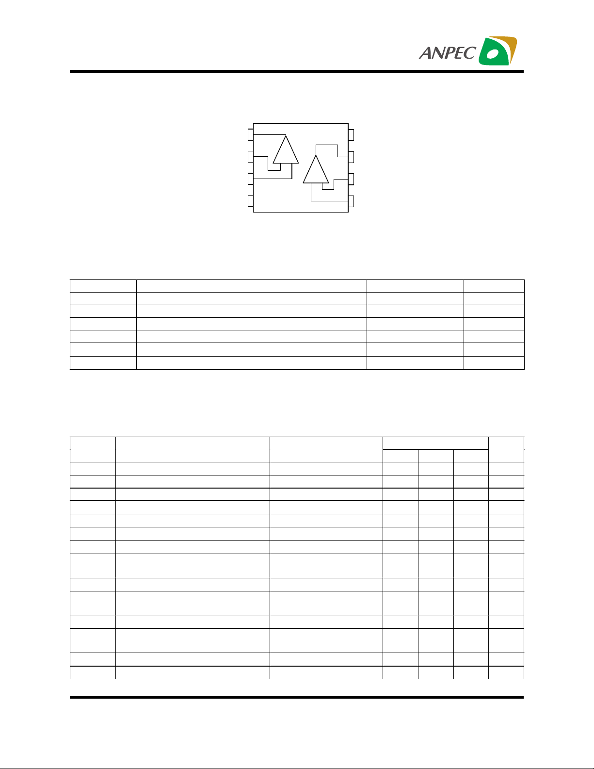
Block Diagram
Output A
Inverting Input A
Non-inverting Input A
1
2
3
-
V
DD
4
-
Absolute Maximum Ratings T
A
+
= 25°C
A
B
-+
+
8
V
DD
7
Output B
6
Inverting Input B
5
Non-inverting Input B
Symbol Parameter Rating Unit
V
DD
V
ID
V
I
P
D
T
A
T
STG
Electrical Characteristics
Supply Voltage 20 V
Differential Input Voltage 20 V
Input Voltage -0.3V to +20V V
Power Dissipation 500 mW
Operating Free-air Temperature Range 0 to 70
Storage Temperature Range -40 to +150
VDD=±10V, TA= 25°C
C
°
C
°
APC558Symbol Parameter Test Conditions
Min. Typ. Max.
13mV
9.5
±
9.5
±
V
V
V
V
I
BIAS
R
A
Input Offset Voltage
IO
I
Input Offset Current 2 10 nA
IO
R
10k
≤
S
Ω
Input Bias Current 25 70 nA
Input Resistance 0.3 5
IN
Large Signal Voltage Gain
V
Maximum Output Voltage Swing 1
OM1
Maximum Output Voltage Swing 2
OM2
Input Common-mode Voltage
ICM
R
R
R
L
10k
≥
L
2k
≥
L
O
Ω±
Ω±
=±10V
, V
≥2kΩ
86 100 dB
9
8.5± 9.0
9
±
Range
CMRR Common-mode Rejection Ratio
SVRR Supply Voltage Rejection Ratio
I
V
Operating Current 3.7 6 mA
CC
Equivalent Input Noise Voltage
NI
R
10k
≤
S
R
10k
≤
S
=100HZ
f
IN
RIAA, R
Ω
Ω,
S
V
=1k
=100mV,
P-P
30kHz,
Ω ,
60 65 dB
90 dB
1.4
µ
LPF
SR Slew Rate 650
mV/µs
GBWP Gain Bandwidth Product 2 MHz
Copyright ANPEC Electronics Corp.
Rev. A.4 - July., 2002
www.anpec.com.tw2
Unit
M
Ω
V
V
V
Vrms
APC558
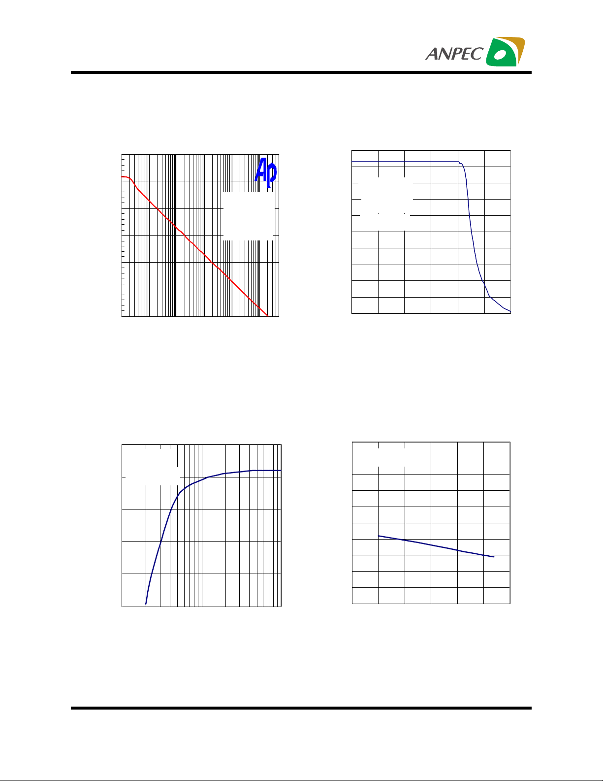
Typical Characteristics
Open Loop Voltage Gain vs Frequency
120
100
80
60
40
20
Open Loop Voltage Gain - dB
0
10 5M100 1k 10k 100k 1M
Frequency (Hz)
Figure 1
Maximum Output Voltage Swing vs Load
Resistance
TA= 25°C
VDD= ±10V
RL=2k
Maximum Output Voltage Swing vs
Frequency
20
18
16
TA= 25°C
14
VDD= ±10V
12
Ω
10
RL=2k
Ω
8
6
4
2
Maximum Output Voltage Swing -V
0
1 10 100 1k 10k 100k 1M
Frequency (Hz)
Figure 2
Operating Current vs Temperature
20
TA= 25°C
VDD= ±10V
18
16
14
12
Maximum Output Voltage Swing - V
10
0.1
0.2 0.5 5
Load Resistance - kΩ
Copyright ANPEC Electronics Corp.
Rev. A.4 - July., 2002
1
Figure 3
10
VDD= ±10V
9
8
7
6
5
4
3
Operating Current - mA
2
1
0
2
10
-50 -25 0 25 50 75 100
Temperature - °C
Figure 4
www.anpec.com.tw3
APC558
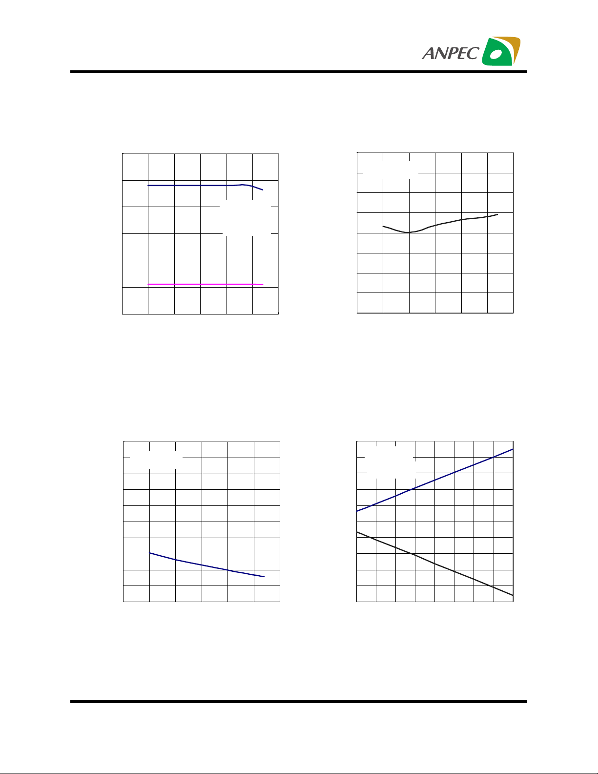
Typical Characteristics Cont.
Maximum Output Voltage Swing vs
Temperature
15
10
5
0
-5
-10
Maximum Output Voltage Swing - V
-15
-50 -25 0 25 50 75 100
Temperature - °C
Figure 5 Figure 6
Input Bias Current vs Temperature
VDD= ±10V
RL=10kΩ
Input Offset Voltage vs Temperature
2
VDD= ±10V
1.5
1
0.5
0
-0.5
-1
Input Offset Voltage - mV
-1.5
-2
-50 -25 0 25 50 75 100
Temperature - °C
Maximum Output Voltage Swing
vs Operating Voltage
100
VDD= ±10V
90
80
70
60
50
40
30
Input Bias Current - nA
20
10
0
-50 -25 0 25 50 75 100
Temperature - °C
Figure 7 Figure 8
Copyright ANPEC Electronics Corp.
Rev. A.4 - July., 2002
10
TA= 25°C
8
Ω
RL=2k
6
4
2
0
-2
-4
-6
-8
Maximum Output Voltage Swing - V
-10
±2±3±4±5±6±7±8±9±
Operating Voltage - V
www.anpec.com.tw4
10

APC558
0
Typical Characteristics Cont.
Operating Current vs Operating Voltage
10
TA= 25°C
9
8
7
6
5
4
3
Operating Current -mA
2
1
0
±2±3±4±5±6±7±8±9±
±
10
Operating Voltage - V
Figure 8
Voltage Follower pulse Response
7.5
5
2.5
0
7.5
5
2.5
0
Input Voltage - V Output Voltage - V
1
0 20 40 60 80 100
Time − µs
Figure 9
Copyright ANPEC Electronics Corp.
Rev. A.4 - July., 2002
www.anpec.com.tw5

APC558
φ
Package Information
PDIP-8 pin ( Reference JEDEC Registration MS-001)
D
E1
1
A
L
e2
e 3
A1
e 1
A2
Millimeters InchesDim
Min. Max. Min. Max.
A
A1
A2
D
e1
e2
e3
E
E1
0.38 0.015
2.92 3.68 0.115 0.145
9.02 10.16 0.355 0.400
2.54BSC 0.100BSC
0.36 0.56 0.014 0.022
1.14 1.78 0.045 0.070
7.62 BSC 0.300 BSC
6.10 7.11 0.240 0.280
E3
L
115
2.92 3.81 0.115 0.150
°
5.33 0.210
10.92 0.430
E
1
E3
15
°
Copyright ANPEC Electronics Corp.
Rev. A.4 - July., 2002
www.anpec.com.tw6

APC558
φ
Package Information
SOP- 8 pin ( Reference JEDEC Registration MS-012)
e1 e2
D
0.004max.
A1
HE
A
0.015X45
1
°
e
L
Millimeters InchesDim
Min. Max. Min. Max.
A 1.35 1.75 0.053 0.069
A1 0.10 0.25 0.004 0.010
D 4.80 5.00 0.189 0.197
E 3.80 4.00 0.150 0.157
H 5.80 6.20 0.228 0.244
L 0.40 1.27 0.016 0.050
e1 0.33 0.51 0.013 0.020
e2 1.27BSC 0.50BSC
18
Copyright ANPEC Electronics Corp.
Rev. A.4 - July., 2002
°
8
°
www.anpec.com.tw7

APC558
φ
φ
φ
Package Information
TSSOP-8
e
8
7
2 x E / 2
S
(2)
(L1)
GAUGE
PLANE
L
1
Dim
12
b
E1 E
e/2
D
A2
A
A1
0.25
(3)
Millimeters Inches
Min. Max. Min. Max.
A 1.2 0.047
A1 0.00 0.15 0.000 0.006
A2 0.80 1.05 0.031 0.041
b 0.19 0.30 0.007 0.012
D 2.9 3.1 0.114 0.122
e 0.65 BSC 0.026 BSC
E 6.40 BSC 0.252 BSC
E1 4.30 4.50 0.169 0.177
L 0.45 0.75 0.018 0.030
L1 1.0 REF 0.039REF
R 0.09 0.004
R1 0.09 0.004
S 0.2 0.008
10
212
312
°
REF 12° REF
°
REF 12° REF
°
8
°
0
°
8
°
Copyright ANPEC Electronics Corp.
Rev. A.4 - July., 2002
www.anpec.com.tw8

APC558
Physical Specifications
Terminal Material Solder-Plated Copper (Solder Material : 90/10 or 63/37 SnPb)
Lead Solderability Meets EIA Specification RSI86-91, ANSI/J-STD-002 Category 3.
Reflow Condition (IR/Convection or VPR Reflow)
Reference JEDEC Standard J-STD-020A APRIL 1999
Peak temperature
temperature
Pre-heat temperature
°
183 C
Time
Classification Reflow Profiles
Convection or IR/
Convection
Average ramp-up rate(183°C to Peak) 3°C/second max. 10 °C /second max.
Preheat temperature 125 ± 25°C)
Temperature maintained above 183°C
Time within 5°C of actual peak temperature
Peak temperature range
Ramp-down rate
Time 25°C to peak temperature
120 seconds max
60 – 150 seconds
10 –20 seconds 60 seconds
220 +5/-0°C or 235 +5/-0°C 215-219°C or 235 +5/-0°C
6 °C /second max. 10 °C /second max.
6 minutes max.
VPR
Package Reflow Conditions
pkg. thickness ≥≥≥≥ 2.5mm
and all bgas
Convection 220 +5/-0 °C Convection 235 +5/-0 °C
VPR 215-219 °C VPR 235 +5/-0 °C
IR/Convection 220 +5/-0 °C IR/Convection 235 +5/-0 °C
Copyright ANPEC Electronics Corp.
Rev. A.4 - July., 2002
pkg. thickness < 2.5mm and
pkg. volume ≥≥≥≥ 350 mm³
pkg. thickness < 2.5mm and pkg.
volume < 350mm³
www.anpec.com.tw9

APC558
Reliability test program
Test item Method Description
SOLDERABILITY MIL-STD-883D-2003
HOLT MIL-STD-883D-1005.7
PCT JESD-22-B, A102
TST MIL-STD-883D-1011.9
ESD MIL-STD-883D-3015.7 VHBM > 2KV, VMM > 200V
Latch-Up JESD 78 10ms , Itr > 100mA
245°C , 5 SEC
1000 Hrs Bias @ 125 °C
168 Hrs, 100 % RH , 121°C
-65°C ~ 150°C, 200 Cycles
Carrier Tape & Reel Dimensions
E
F
W
Po
A
P
P1
Ao
J
t
D
Bo
Ko
D1
T2
C
B
Application
A B C J T1 T2 W P E
330±1 62 ± 1.5
SOP-8
F D D1 Po P1 Ao Bo Ko t
5.5 ± 0.1 1.55 ±+0.1
Application
A B C J T1 T2 W P E
330 ± 1 62 +1.5
TSSOP-8
F D D1 Po P1 Ao Bo Ko t
5.5 ± 0. 1 1.5 + 0.1 1.5 + 0.1 4.0 ± 0.1 2.0 ± 0.1 7.0 ± 0.1 3.6 ± 0.3 1.6 ± 0.1 0.3±0.013
Copyright ANPEC Electronics Corp.
Rev. A.4 - July., 2002
12.75
+0.15
1.55+0.25
12.75+
0.15
T1
2 + 0.5 12.4 +0.2
2± 0.2
12 + 0.3
8± 0.1 1.75± 0.1
- 0.1
4.0 ± 0.1 2.0 ± 0.1 6.4 ± 0.1 5.2± 0.1 2.1± 0.1 0.3±0.013
2 + 0.5 12.4 ± 0.2 2 ± 0.2 12± 0. 3 8± 0.1 1.75±0.1
(mm)
www.anpec.com.tw10

APC558
Cover Tape Dimensions
Application Carrier Width Cover Tape Width Devices Per Reel
SOP- 8
TSSOP- 8
Customer Service
Anpec Electronics Corp.
Head Office :
5F, No. 2 Li-Hsin Road, SBIP,
Hsin-Chu, Taiwan, R.O.C.
Tel : 886-3-5642000
Fax : 886-3-5642050
Taipei Branch :
7F, No. 137, Lane 235, Pac Chiao Rd.,
Hsin Tien City, Taipei Hsien, Taiwan, R. O. C.
Tel : 886-2-89191368
Fax : 886-2-89191369
12 9.3 2500
12 9.3 2500
Copyright ANPEC Electronics Corp.
Rev. A.4 - July., 2002
www.anpec.com.tw11
 Loading...