Evaluation Board User Guide
One Technology Way • P. O . Box 9106 • Norwood, MA 02062-9106, U.S.A. • Tel : 781.329.4700 • Fax : 781.461.3113 • www.analog.com
UG-186
User Guide for ADP322/ADP323 Evaluation Board
FEATURES
Bias voltage range (V
LDO input voltage range (V
Output current range: 0 mA to 200 mA per output
Output voltage accuracy: ±1%
Operating temperature range: −40°C to +125°C
): 2.5 V to 5.5 V
BIAS
IN1/VIN2
, V
): 1.8 V to 5.5 V
IN3
GENERAL DESCRIPTION
The ADP322/ADP323 evaluation board is used to demonstrate the
functionality of the ADP322/ADP323 series of linear regulators.
Simple device measurements, such as line and load regulation,
dropout voltage, and ground current, can be demonstrated with
two voltage supplies, a few voltmeters, current meters, and load
resistors.
For more details about the ADP322/ADP323 linear regulators,
see the ADP322/ADP323 data sheet.
EVALUATION BOARD
PLEASE SEE THE LAST PAGE FOR AN IMPORTANT
WARNING AND LEGAL TERMS AND CONDITIONS.
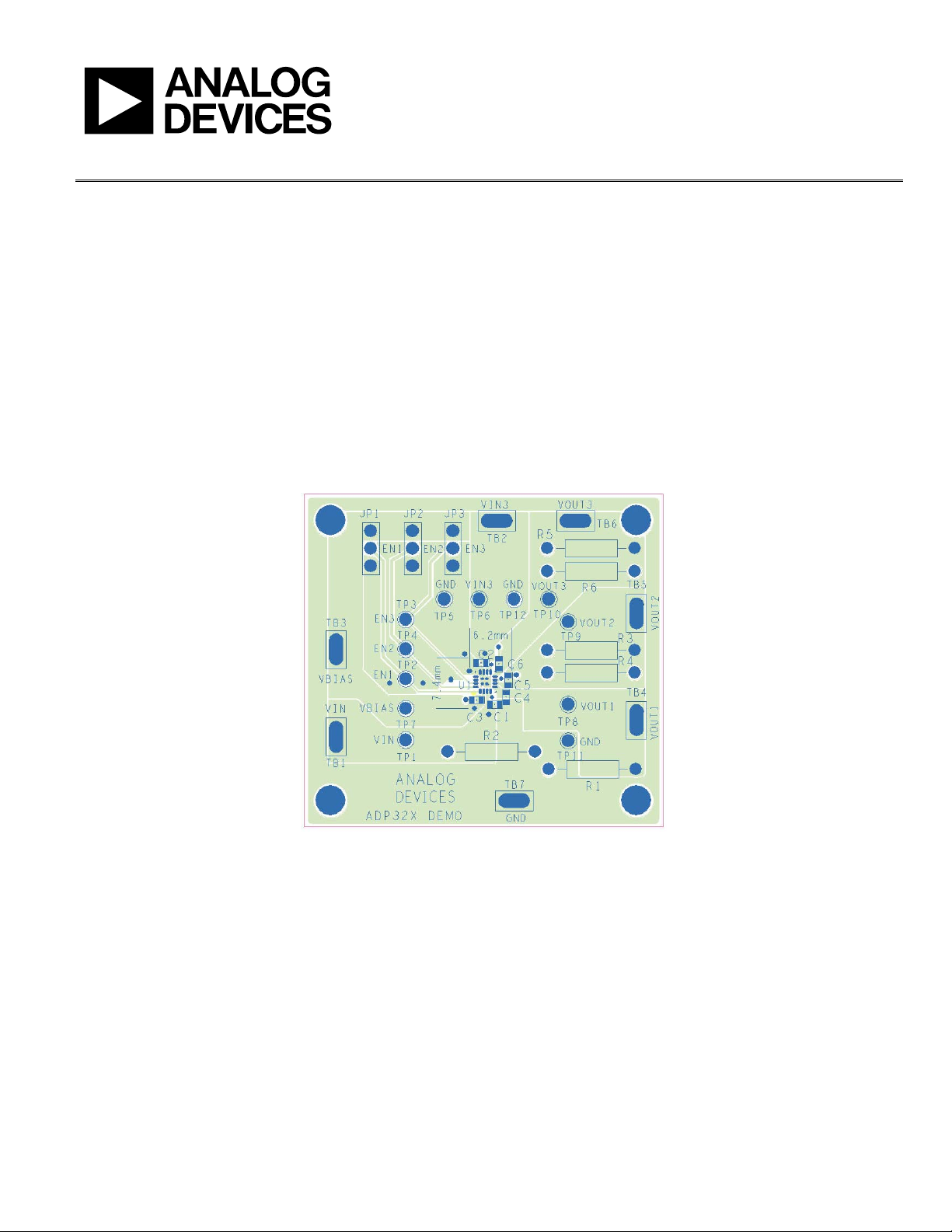
Figure 1. ADP322/ADP323 Evaluation Board
Rev. 0 | Page 1 of 12
9299-001

UG-186 Evaluation Board User Guide
TABLE OF CONTENTS
Features.............................................................................................. 1
General Description ......................................................................... 1
Evaluation Board .............................................................................. 1
Revision History ............................................................................... 2
Evaluation Board Hardware and Schematic ................................. 3
Output Voltage Measurements ....................................................... 4
Line Regulation Measurements.................................................. 4
Load Regulation Measurements................................................. 5
REVISION HISTORY
10/10—Revision 0: Initial Version
Dropout Voltage Measurements..................................................5
Ground and Bias Current Measurements ......................................6
Ground Current Measurement....................................................6
Bias Current Measurement ..........................................................7
Printed Circuit Board Layout Considerations...............................8
Ordering Information.......................................................................9
Bill of Materials..............................................................................9
Related Links......................................................................................9
Rev. 0 | Page 2 of 12

Evaluation Board User Guide UG-186
EVALUATION BOARD HARDWARE AND SCHEMATIC
1
1µF
1
C2
1
C1
1
EN1
EN3
VIN
TP5
TP6
TP7
VBIAS
C3
1µF
EN2
TP1
VIN3
U1
ADP322/ADP323
2
VBIAS
3
VIN1/VIN2
10
VIN3
1
EN1
16
EN2
15
EN3
NC
GND
11
12
1
TP2
1
TP3
1
TP4
VOUT1
FB1/NC
VOUT2
FB2/NC
VOUT3
FB3/NC
NC
NC
PAD
PAD
5
4
6
7
8
9
14
13
R2
RES
1 2
1 2
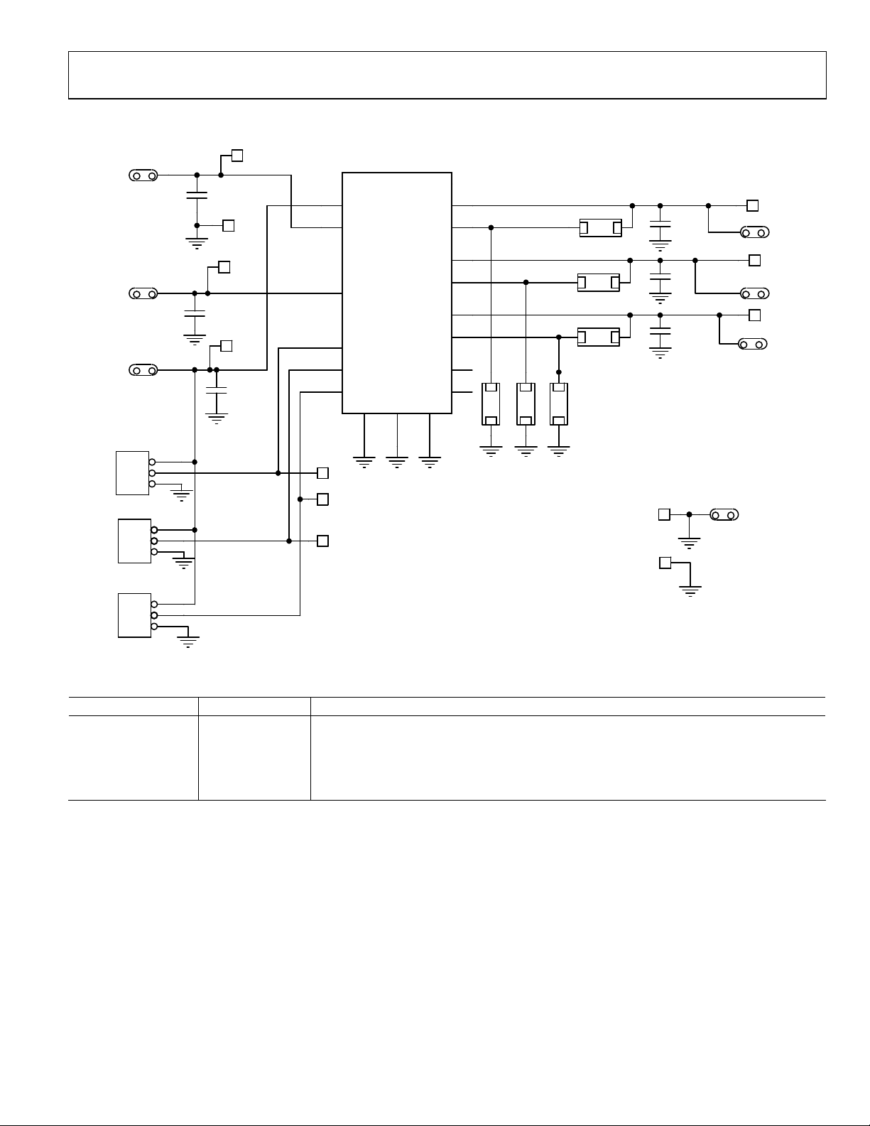
Figure 2. ADP322/ADP323 Evaluation Board Schematic
RES
R4
R1
1 2
R3
1 2
R5
1 2
2
R6
RES
1
RES
RES
RES
TP11
TP12
C4
1µF
C5
1µF
C6
1µF
1
VOUT1
VOUT2
VOUT3
1
TB7
1
1
1
TB4
TB5
TB6
GND
TP8
TP9
TP10
09299-002
TB1
TB2
TB3
JP1
1
2
3
HEADER_3
JP2
HEADER_3
JP3
HEADER_3
1µF
1
2
3
1
1
2
2
3
3
1
1
2
2
3
3
Table 1. Evaluation Board Hardware Components
Component Function Description
U11 Linear regulator ADP322/ADP323 low dropout linear regulator.
C1, C2, C3, C4, C5, C6 Input capacitor 1 μF input bypass capacitor, 0402 or 0603 case.
JP1, JP2, JP3 3-pin jumper These jumpers connect EN1, EN2, and EN3 to VBIAS for automatic startup.
R1, R2, R3, R4, R5, R6 Resistor
Resistors for setting output voltage for the ADP323, 0603 size. Short R1, R3, and R5 to connect
the output voltage to the feedback input for the ADP322.
1
Component varies depending on the evaluation board type ordered.
Rev. 0 | Page 3 of 12

UG-186 Evaluation Board User Guide
OUTPUT VOLTAGE MEASUREMENTS
VOLTMETER
1.99711
VOLTMETER VOLTMETER
1.99711 1.99711
VOLTAGE SOURCE
VOLTAGE SOURCE
VOLTMETER
1.99711
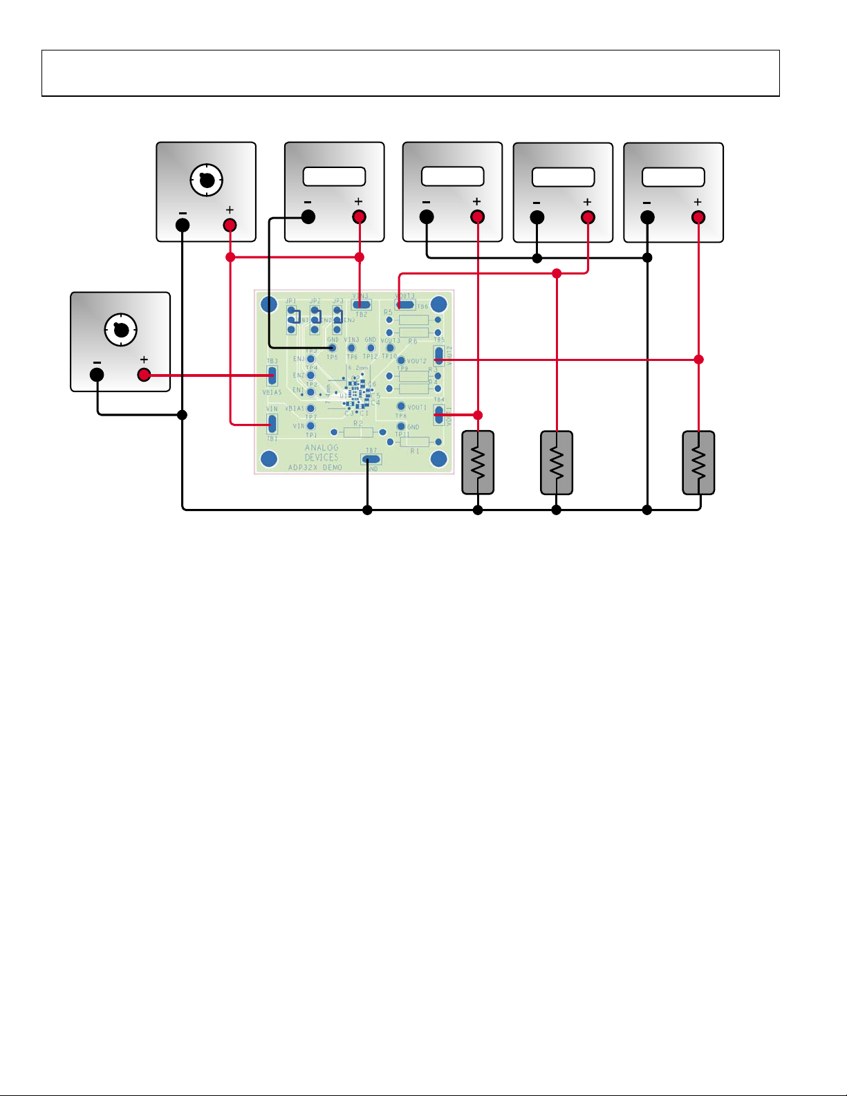
Figure 3. Output Voltage Measurement Setup
Figure 3 shows how the evaluation board can be connected to a
voltage source and voltmeters for basic output voltage accuracy
measurements. A resistor can be used as the load for the regulator. Ensure that the resistor has a power rating adequate to handle
the power expected to be dissipated across it. An electronic load
can be used as an alternative. In addition, ensure that the voltage
source can supply enough current for the expected load levels.
Follow these steps to connect to a voltage source and voltmeters:
1. Insert R1, R2, R3, R4, R5, and R6 to set voltages for an
ADP323. If an ADP322 is used, short R1, R3, and R5
to connect the output voltages to the feedback input for
each LDO.
2. Insert Jumpers JP1, JP2, and JP3 for automatic startup.
3. Connect the negative terminal (−) of the voltage sources to
one of the GND pads on the evaluation board.
4. Connect the positive terminal (+) of the main voltage
source to the VIN and VIN3 pads of the evaluation board.
5. Connect the positive terminal (+) of the bias voltage source
to the VBIAS pad of the evaluation board. Set the bias
voltage supply to a voltage from 2.5 V to 5.5 V.
6. Connect a load between VOUT1, VOUT2, and/or VOUT3
and one of the GND pads.
LOAD
LOAD LOAD
09299-003
7. Connect the negative terminal (−) of the voltmeters to one
of the GND pads.
8. Connect the positive terminal (+) of the voltmeters to
VOUT1, VOUT2, and/or VOUT3 and VIN/VIN3.
The voltage sources can now be turned on.
LINE REGULATION MEASUREMENTS
For line regulation measurements, the regulator’s outputs are
monitored while its input is varied. For good line regulation,
the outputs must change as little as possible with varying input
levels. To ensure that the device is not in dropout mode during
this measurement, V
(or 1.8 V, whichever is greater) and V
highest of the three output voltages. For example, for an ADP322/
ADP323 with a fixed 1.8 V output, V
2.3 V and 5.5 V. This measurement can be repeated under different
load conditions. Figure 4 shows the typical line regulation performance of the ADP322/ADP323 with a fixed 1.8 V output.
must be varied between V
IN
, where V
INMAX
must be varied between
IN
OUTNOM
OUTNOM
+ 0.5 V
is the
Rev. 0 | Page 4 of 12
 Loading...