Analog Devices SSM2122, SSM2120 Datasheet

SIGNAL
OUT
CURRENT
MIRRORS
–V
C
+V
C
V+
V+
V+
SIGNAL
INPUT
36kΩ
36kΩ
V+
V–
I
REF
Dynamic Range
13
16
15
14
22
21
20
19
18
17
12
TOP VIEW
(Not to Scale)
11
10
9
8
1
2
3
4
7
6
5
SSM2120
THRESH 1
+V
C2
SIG
OUT 2
V+
GND
LOG AV 1
CON
OUT 1
SIG
OUT 1
SIG
IN 2
–V
C2
CFT 2
+V
C1
CFT 1
–V
C1
SIG
IN 1
REC
IN 1
I
REF
LOG AV 2
CON
OUT 2
REC
IN 2
V– THRESH 2
14
13
12
11
16
15
10
9
8
1
2
3
4
7
6
5
TOP VIEW
(Not to Scale)
SSM2122
GND
+V
C2
SIG
OUT 2
V+
GND
SIG
OUT 1
+V
C1
CFT 1
SIG
IN 2
–V
C2
CFT 2
–V
C1
SIG
IN 1
I
REF
V–
GND
a
FEATURES
0.01% THD at +10 dBV In/Out
100 dB VCA Dynamic Range
Low VCA Control Feedthrough
100 dB Level Detection Range
Log/Antilog Control Paths
Low External Component Count
APPLICATIONS
Compressors
Expanders
Limiters
AGC Circuits
Voltage-Controlled Filters
Noise Reduction Systems
Stereo Noise Gates
GENERAL DESCRIPTION
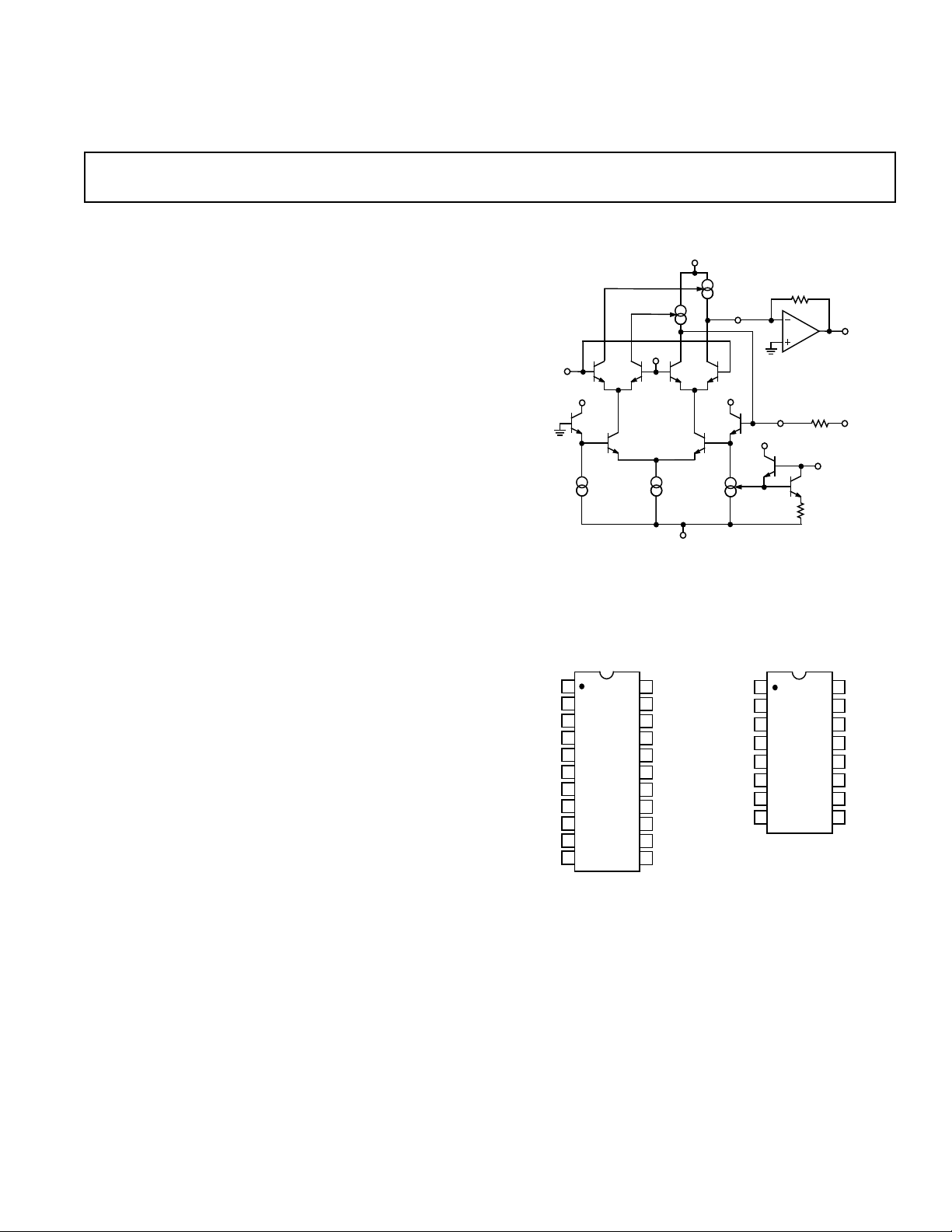
The SSM2120 is a monolithic integrated circuit designed for the
purpose of processing dynamic signals in various analog systems
including audio. This “dynamic range processor” consists of two
VCAs and two level detectors (the SSM2122 consists of two
VCAs only). These circuit blocks allow the user to logarithmically
control the gain or attenuation of the signals presented to the
level detectors depending on their magnitudes. This allows the
compression, expansion or limiting of ac signals, some of the
primary applications for the SSM2120.
Processors/Dual VCA
SSM2120/SSM2122
FUNCTIONAL BLOCK DIAGRAM
PIN CONNECTIONS
22-Pin Plastic DIP
(P Suffix)
16-Pin Plastic DIP
(P Suffix)
REV. C
Information furnished by Analog Devices is believed to be accurate and
reliable. However, no responsibility is assumed by Analog Devices for its
use, nor for any infringements of patents or other rights of third parties
which may result from its use. No license is granted by implication or
otherwise under any patent or patent rights of Analog Devices.
One Technology Way, P.O. Box 9106, Norwood, MA 02062-9106, U.S.A.
Tel: 617/329-4700 Fax: 617/326-8703
© Analog Devices, Inc., 1995

SSM2120/SSM2122–SPECIFICATIONS
(@VS = 615 V, TA = +258C, I
ELECTRICAL CHARACTERISTICS
unless otherwise noted)
Parameter Conditions Min Typ Max Units
POWER SUPPLY
Supply Voltage Range ±5 ±18 V
Positive Supply Current 810mA
Negative Supply Current –6 –8 mA
VCAs
Max I
(In/Out) ±300 ±325 ±350 µA
SIGNAL
Output Offset ±1 ±8 µA
Control Feedthrough (Trimmed) R
IN
= R
= 36 kΩ, –30 dB ≤ AV ≤ 0 dB ±750 µV
OUT
Gain Control Range Unity-Gain –85 +40 dB
Control Sensitivity 6 mV/dB
Gain Scale Factor Drift –3300 ppm/°C
Frequency Response Unity Gain or Less 250 kHz
Off Isolation At 1 kHz 100 dB
Current Gain +V
= –VC = 0 V –0.5 +0.5 dB
C
THD (Unity-Gain) +10 dBV IN/OUT 0.005 0.04 %
Noise (20 kHz Bandwidth) RE: 0 dBV –80 dB
LEVEL DETECTORS (SSM2120 ONLY)
Detection Range 90 95 dB
Input Current Range 0.085 2800 µA p-p
Rectifier Input Bias Current 4nA
Output Sensitivity (At LOG AV Pin) 3 mV/dB
Output Offset Voltage ±0.5 ±3.4 mV
Frequency Response
I
= 1 mA p-p 1000
IN
I
= 10 µA p-p 50 kHz
IN
I
= 1 µA p-p 7.5
IN
CONTROL AMPLIFIERS (SSM2120 ONLY)
Input Bias Current ±85 ±175 nA
Output Drive (Max Sink Current) 5.0 7.5 mA
Input Offset Voltage ±0.5 ±4.2 mV
Specifications are subject to change without notice.
= 200 mA, +VC = –VC = GND (AV = 0 dB). 0 dB = 1 V rms
REF
SSM2120/SSM2122
ABSOLUTE MAXIMUM RATINGS
Supply Voltage . . . . . . . . . . . . . . . . . . . . . . . . . . . . . . . . ±18 V
Operating Temperature Range . . . . . . . . . . . . –10°C to +55°C
Junction Temperature . . . . . . . . . . . . . . . . . . . . . . . . . +150°C
Storage Temperature . . . . . . . . . . . . . . . . . . –65°C to +150°C
Maximum Current into Any Pin . . . . . . . . . . . . . . . . . . 10 mA
Lead Temperature Range (Soldering, 60 sec) . . . . . . . +300°C
Package Type θ
1
JA
θ
JC
Units
Model Range Description Option
SSM2120 –10°C to +50°C 22-Pin Plastic DIP (N-22)
SSM2122 –10°C to +50°C 16-Pin Plastic DIP (N-16)
ORDERING GUIDE
Temperature Package Package
16-Pin Plastic DIP (P) 86 10 °C/W
22-Pin Plastic DIP (P) 70 7 °C/W
NOTE
1
θJA is specified for worst case mounting conditions, i.e., θJA is specified for
device in socket for P-DIP.
CAUTION
ESD (electrostatic discharge) sensitive device. Electrostatic charges as high as 4000 V readily
accumulate on the human body and test equipment and can discharge without detection.
Although the SSM2120/SSM2122 features proprietary ESD protection circuitry, permanent damage
may occur on devices subjected to high energy electrostatic discharges. Therefore, proper ESD
precautions are recommended to avoid performance degradation or loss of functionality.
–2–
WARNING!
ESD SENSITIVE DEVICE
REV. C

+V
GAIN – dB
0.03
THD – %
0.01
–20 20–10 0 10
0.003
C1
INPUT 1 OUTPUT 1
–V
C1
+V
C2
INPUT 2 OUTPUT 2
–V
C2
SSM2122
CFT 1
CFT 2
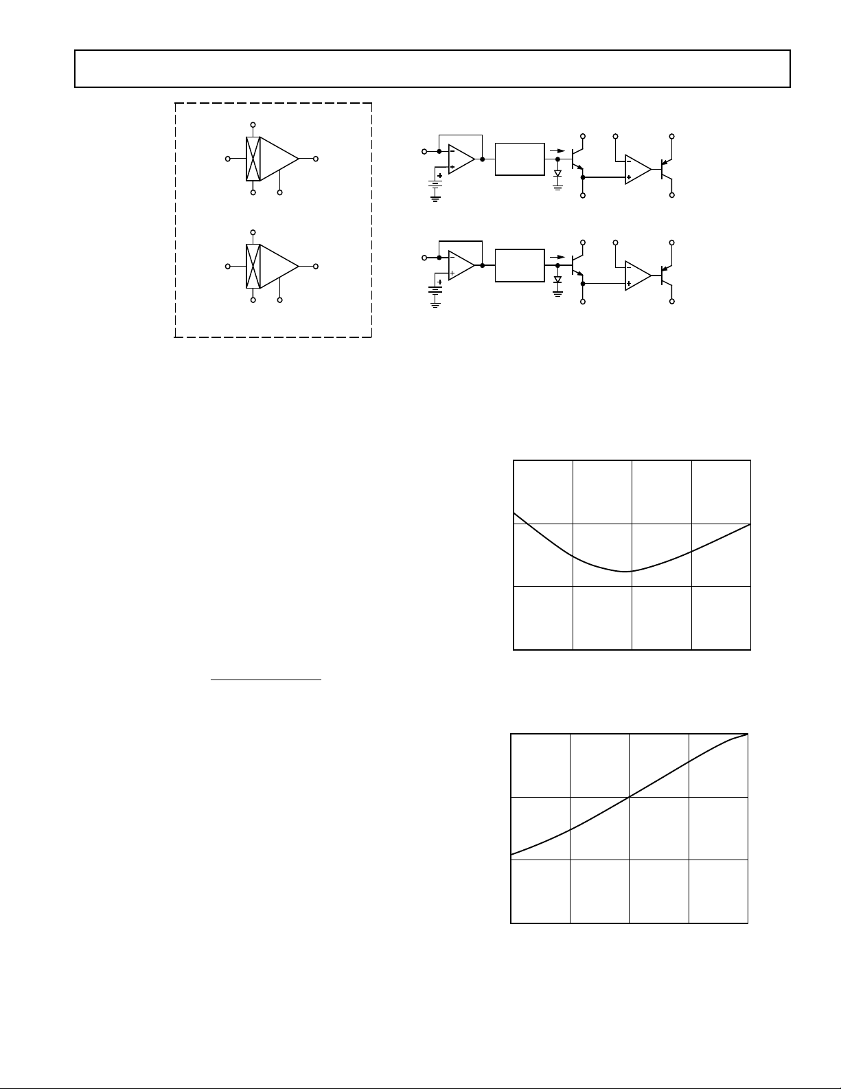
Figure 1. SSM2120 Block Diagram
REC
REC
IN 1
IN 2
SSM2120/SSM2122
V+ THRESH 1
|IIN|
FULL
WAVE
RECTIFIER
2V
LOG AV 1
V+ THRESH 2
|IIN|
FULL
WAVE
RECTIFIER
2V
LOG AV 2
CON
CON
OUT 1
V–
OUT 2
V–
VOLTAGE-CONTROLLED AMPLIFIERS
The two voltage-controlled amplifiers are full Class A current
in/current out devices with complementary dB/V gain control
ports. The control sensitivities are +6 mV/dB and –6 mV/dB. A
resistor divider (attenuator) is used to adapt the sensitivity of an
external control voltage to the range of the control port. It is
best to use 200 Ω or less for the attenuator resistor to ground.
VCA INPUTS
The signal inputs behave as virtual grounds. The input current
compliance range is determined by the current into the reference
current pin.
REFERENCE PIN
The reference current determines the input and output current
compliance range of the VCAs. The current into the reference
pin is set by connecting a resistor to V+. The voltage at the
reference pin is about two volts above V– and the current will be
[(V +)–((V–)+2V )]
=
I
REF
R
REF
The current consumption of the VCAs will be directly proportional to I
which is nominally 200 µA. The device will
REF
operate at lower current levels which will reduce the effective
dynamic range of the VCAs. With a 200 µA reference current,
the input and output clip points will be ± 400 µA. In general:
I
= ±2 I
CLIP
REF
VCA OUTPUTS
The VCA outputs are designed to interface directly with the virtual
ground inputs of external operational amplifiers configured as
current-to-voltage converters. The outputs must operate at virtual
ground because of the output stage’s finite output impedance.
The power supplies and selected compliance range determines
the values of input and output resistors needed. As an example,
with ±15 V supplies and ±400 µA maximum input and output
current, choose R
IN
= R
= 36 kΩ for an output compliance
OUT
range of ±14.4 V. Note that the signal path through the VCA
including the output current-to-voltage converter is noninverting.
VCA PERFORMANCE
Figures 2a and 2b show the typical THD and noise performance
of the VCAs over ±20 dB gain/attenuation. Full Class A operation
provides very low THD.
a. VCA THD Performance vs. Gain
(+10 dBV In/Out @ 1 kHz)
–70
–80
NOISE – dBV
–90
–20 20–10 0 10
GAIN – dB
b. VCA Noise vs. Gain (20 kHz Bandwidth)
Figure 2. Typical THD and Noise Performance
REV. C
–3–

SSM2120/SSM2122
TRIMMING THE VCAs
The control feedthrough (CFT) pins are optional control feedthrough null points. CFT nulling is usually required in applications
such as noise gating and downward expansion. If trimming is
not used, leave the CFT pins open.
Trim Procedure
1. Apply a 100 Hz sine wave to the control point attenuator.
The signal peaks should correspond to the control voltages
which induce the VCAs maximum intended gain and at least
30 dB of attenuation.
2. Adjust the 50 kΩ potentiometer for the minimum
feedthrough.
(Trimmed control feedthrough is typically well under 1 mV rms
when the maximum gain is unity using 36 kΩ input and output
resistors.)
Applications such as compressor/limiters typically do not require
control feedthrough trimming because the VCA operates at
unity-gain unless the signal is large enough to initiate gain
reduction. In this case the signal masks control feedthrough.
This trim is ineffective for voltage-controlled filter applications.
LEVEL DETECTION CIRCUITS
The SSM2120 contains two independent level detection
circuits. Each circuit contains a wide dynamic range full-wave
rectifier, logging circuit and a unipolar drive amplifier. These
circuits will accurately detect the input signal level over a
100 dB range from 30 nA to 3 mA peak-to-peak.
LEVEL DETECTOR THEORY OF OPERATION
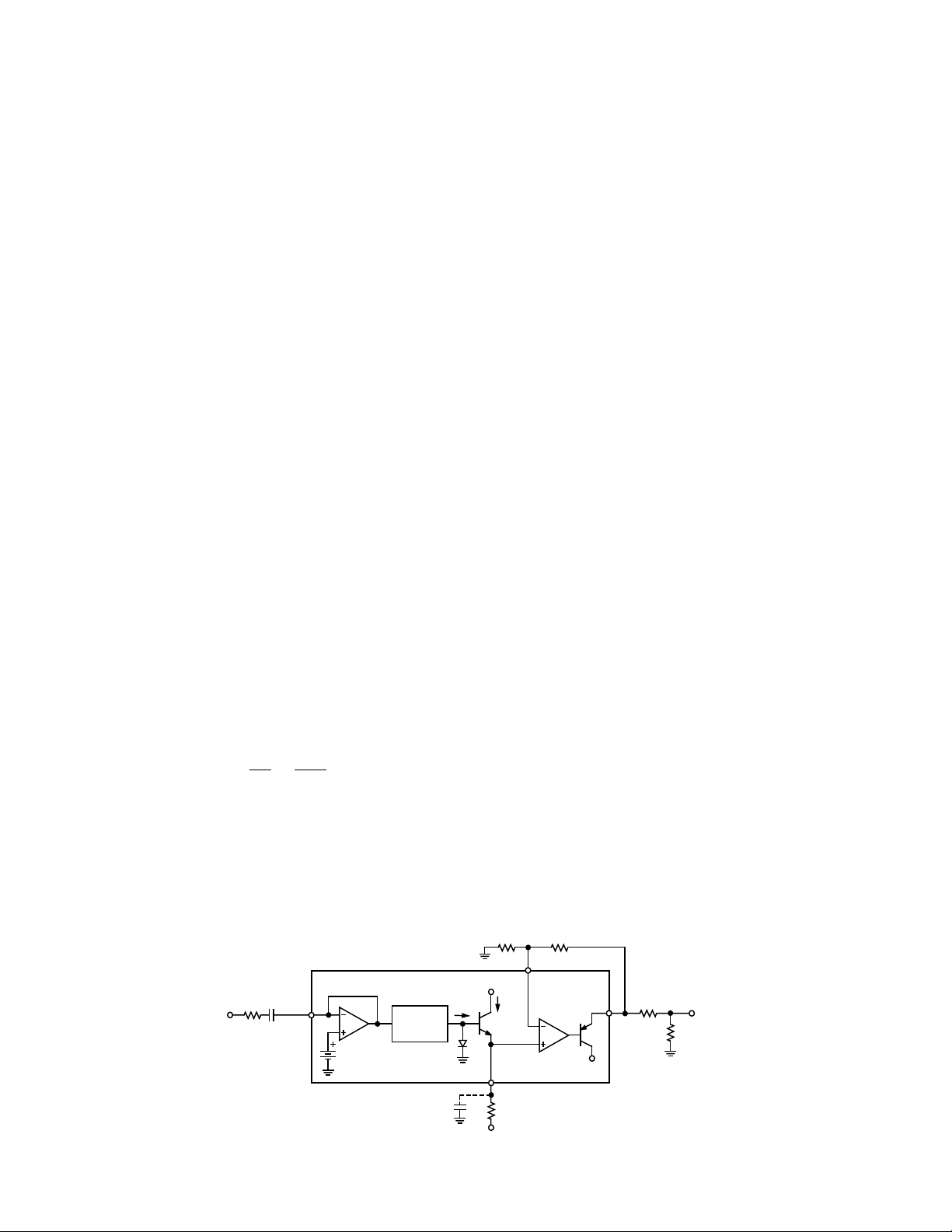
Referring to the level detector block diagram of Figure 3, the
REC
input is an AC virtual ground. The next block imple-
IN
ments the full-wave rectification of the input current. This
current is then fed into a logging transistor (Q
transistor (Q
) has a fixed collector current of I
2
) whose pair
1
. The LOG
REF
AV output is then:
AV =
kT
q
V
LOG
ln
|
|I
IN
I
REF
With the use of the LOG AV capacitor the output is then the log
of the average of the absolute value of I
.
IN
(The unfiltered LOG AV output has broad flat plateaus with
sharp negative spikes at the zero crossing. This reduces the
“work” that the averaging capacitor must do, particularly at low
frequencies.)
Note: It is natural to assume that with the addition of the
averaging capacitor, the LOG AV output would become the
average of the log of the absolute value of I
. However, since the
IN
capacitor forces an ac ground at the emitter of the output
transistor, the capacitor charging currents are proportional to
the antilog of the voltage at the base of the output transistor.
Since the base voltage of the output transistor is the log of the
absolute value of I
, the log and antilog terms cancel, so the
IN
capacitor becomes a linear integrator with a charging current
directly proportional to the absolute value of the input current.
This effectively inverts the order of the averaging and logging
functions. The signal at the output therefore is the log of the
average of the absolute value of I
.
IN
USING DETECTOR PINS RECIN, LOGAV, THRESH AND
CON
OUT
When applying signals to RECIN (rectifier input) an input series
resistor should be followed by a low leakage blocking capacitor
since REC
ground. Choose R
has a dc voltage of approximately 2.1 V above
IN
for a ±1.5 mA peak signal. For ± 15 V
IN
operation this corresponds to a value of 10 kΩ.
A 1.5 MΩ value of R
a 10 µA reference current in the logging transistor (Q
from log average to –15 V will establish
REF
). This
1
will bias the transistor in the middle of the detector’s dynamic
current range in dB to optimize dynamic range and accuracy.
The LOG AV outputs are buffered and amplified by unipolar
drive op amps. The 39 kΩ, 1 kΩ resistor network at the
THRESH pin provides a gain of 40.
An attenuator from the CON
(control output) to the
OUT
appropriate VCA control port establishes the control sensitivity.
Use 200 Ω for the attenuator resistor to ground and choose
R
for the desired sensitivity. Care should be taken to minimize
CON
capacitive loads on the control outputs CON
. If long lines
OUT
or capacitive loads are present, it is best to connect the series
resistor R
as closely to the CON
CON
pin as possible.
OUT
DYNAMIC LEVEL DETECTOR CHARACTERISTICS
Figures 4 and 5 show the dynamic performance of the level
detector to a change in signal level. The input to the detector (not
shown) is a series of 500 ms tone bursts at 1 kHz in successive
10 dBV steps. The tone bursts start at a level of –60 dBV (with
R
= 10 k) and return to –60 dBV after each successive 10 dB
IN
step. Tone bursts range from –60 dBV to +10 dBV. Figure 4
shows the logarithmic level detector output. The output of the
detector is 3 mV/dB at LOG AV and the amplifier gain is 40
which yields 120 mV/dB. Thus, the output at CON
OUT
is seen
to increase by 1.2 V for each 10 dBV increase in input level.
1kΩ
39kΩ
INPUT
I
REF
LOG AV
R
REF
THRESH
CON
OUT
V–
R
CON
200Ω
TO V
C
V+
R
REC
IN
IN
RECTIFIER
2V
FULL
WAVE
|IIN|
Q2
Q1
C
AV
V–
Figure 3. Level Detector
–4–
REV. C
 Loading...