Ultraprecision
V
www.BDTIC.com/ADI
FEATURES
Ultralow offset voltage
= 25°C, 25 μV maximum
T
A
Outstanding offset voltage drift 0.1 μV/°C maximum
Excellent open-loop gain and gain linearity
12 V/μV typical
CMRR: 130 dB minimum
PSRR: 115 dB minimum
Low supply current 2.0 mA maximum
Fits industry-standard precision op amp sockets
GENERAL DESCRIPTION
The OP177 features one of the highest precision performance of
any op amp currently available. Offset voltage of the OP177 is
only 25 μV maximum at room temperature. The ultralow V
the OP177 combines with its exceptional offset voltage drift
(TCV
) of 0.1 μV/°C maximum to eliminate the need for
OS
external V
adjustment and increases system accuracy over
OS
temperature.
The OP177 open-loop gain of 12 V/μV is maintained over the
ull ±10 V output range. CMRR of 130 dB minimum, PSRR of
f
120 dB minimum, and maximum supply current of 2 mA are
just a few examples of the excellent performance of this
of
OS
Operational Amplifier
OP177
PIN CONFIGURATION
1
TRIM VOS TRIM
OS
OP177
2
–IN
3
+IN
TOP VIEW
4
(Not to Scale)
NC = NO CONNECT
Figure 1. 8-Lead PDIP (P-Suffix),
8-Lead
SOIC (S-Suffix)
operational amplifier. The combination of outstanding
s
pecifications of the OP177 ensures accurate performance in
high closed-loop gain applications.
This low noise, bipolar input op amp is also a cost effective
ternative to chopper-stabilized amplifiers. The OP177
al
provides chopper-type performance without the usual problems
of high noise, low frequency chopper spikes, large physical size,
limited common-mode input voltage range, and bulky external
storage capacitors.
The OP177 is offered in the −40°C to +85°C extended industrial
t
emperature ranges. This product is available in 8-lead PDIP, as
well as the space saving 8-lead SOIC.
8
7
V+
6
OUT
5
NCV–
00289-001
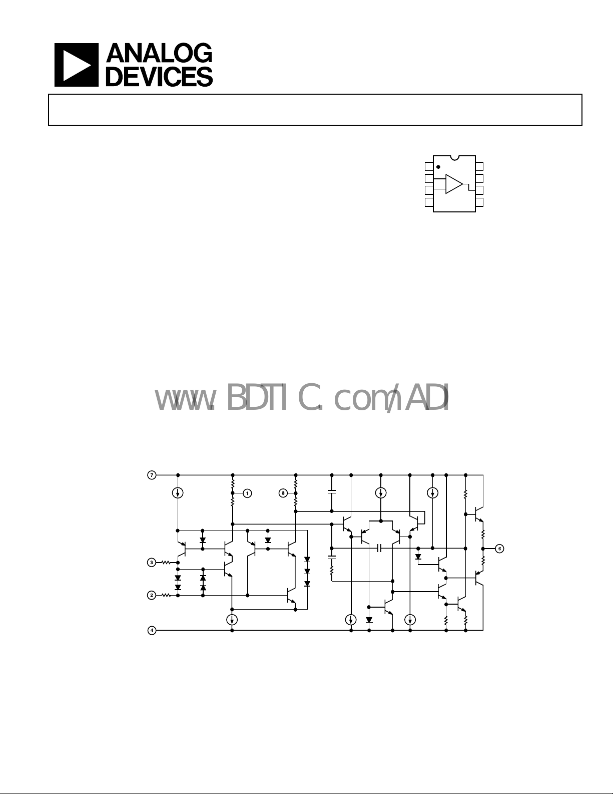
FUNCTIONAL BLOCK DIAGRAM
V+
2B
Q
5
R
NONINVERTI NG
INPUT
INVERTING
INPUT
3
Q
21
Q
R
22
4
V–
Rev. E
Information furnished by Analog Devices is believed to be accurate and reliable. However, no
responsibility is assumed by Anal og Devices for its use, nor for any infringements of patents or ot her
rights of third parties that may result from its use. Specifications subject to change without notice. No
license is granted by implication or otherwise under any patent or patent rights of Analog Devices.
Trademarks and registered trademarks are the property of their respective owners.
(OPTIO NAL NULL)
R
1A
Q
7
Q
3
Q
1
Q
23
Q
24
AND R2BARE ELECTRONI CALLY ADJUST ED ON CHIP AT F ACTORY.
*R
2A
Q
8
Q
6
Q
Q
Figure 2. Simplified Schematic
R2B*R2A*
R
1B
4
2
C
1
Q
9
Q11Q
C
3
Q
27
R
5
Q
26
Q
25
Q
10
12
C
2
Q
Q
13
Q
17
14
R
7
Q
19
R
9
OUTPUT
R
Q
16
Q
15
R
6
10
Q
20
Q
18
R
8
00289-002
One Technology Way, P.O. Box 9106, Norwood, MA 02062-9106, U.S.A.
Tel: 781.329.4700 www.analog.com
Fax: 781.461.3113 ©2006 Analog Devices, Inc. All rights reserved.

OP177
www.BDTIC.com/ADI
TABLE OF CONTENTS
Features .............................................................................................. 1
Gain Linearity................................................................................9
Pin Configuration............................................................................. 1
General Description......................................................................... 1
Functional Block Diagram .............................................................. 1
Revision History ............................................................................... 2
Specifications..................................................................................... 3
Electrical Characteristics............................................................. 3
Test Cir c ui t s ................................................................................... 4
Absolute Maximum Ratings............................................................ 5
Thermal Resistance ...................................................................... 5
ESD Caution.................................................................................. 5
Typical Performance Characteristics ............................................. 6
Application Information.................................................................. 9
REVISION HISTORY
5/06—Rev. D to Rev. E
Changes to Figure 1.......................................................................... 1
Change to Specifications Table 1 .................................................... 3
Changes to Specifications Table 2................................................... 4
Changes to Table 3............................................................................ 5
Changes to Figure 23 and Figure 24............................................... 9
Changes to Figure 32...................................................................... 12
Updated the Ordering Guide........................................................ 14
4/06—Rev. C to Rev. D
hange to Pin Configuration Caption........................................... 1
C
Changes to Features.......................................................................... 1
Change to Table 2 ............................................................................. 4
Change to Figure 2 ........................................................................... 4
Changes to Figure 10 and Figure 11............................................... 6
Changes to Figure 12 through Figure 17....................................... 7
Changes to Figure 18 through Figure 22....................................... 8
Thermocouple Amplifier with Cold-Junction
Compensation................................................................................9
Precision High Gain Differential Amplifier ........................... 10
Isolating Large Capacitive Loads.............................................. 10
Bilateral Current Source............................................................ 10
Precision Absolute Value Amplifier......................................... 10
Precision Positive Peak Detector.............................................. 12
Precision Threshold Detector/Amplifier ................................ 12
Outline Dimensions ....................................................................... 13
Ordering Guide .......................................................................... 14
Change to Figure 27....................................................................... 10
Changes to Figure 30 and Figure 31............................................. 11
Updated Outline Dimensions....................................................... 13
Changes to Ordering Guide.......................................................... 13
1/05—Re
Edits to Features.................................................................................1
dits to General Description ...........................................................1
E
Edits to Pin Connections..................................................................1
Edits to Electrical Characteristics .............................................. 2, 3
Global deletion of references to OP177E............................ 3, 4, 10
Edits to Absolute Maximum Ratings..............................................5
Edits to Package Type .......................................................................5
Edits to Ordering Guide...................................................................5
Edit to Outline Dimensions.......................................................... 11
11/95—Rev. 0: Initial Version
v. B to Rev. C
Rev. E | Page 2 of 16

OP177
www.BDTIC.com/ADI
SPECIFICATIONS
ELECTRICAL CHARACTERISTICS
@ VS = ±15 V, TA = 25°C, unless otherwise noted.
Table 1.
OP177F OP177G
Parameter Symbol Conditions Min Typ Max Min Typ Max Unit
INPUT OFFSET VOLTAGE V
LONG-TERM INPUT OFFSETT
1
OS
10 25 20 60 μV
Voltage Stability ΔVOS/time 0.3 0.4 μV/mo
INPUT OFFSET CURRENT I
INPUT BIAS CURRENT I
OS
B
INPUT NOISE VOLTAGE en fO = 1 Hz to 100 Hz
INPUT NOISE CURRENT i
n
0.3 1.5 0.3 2.8 nA
−0.2 +1.2 +2 −0.2 +1.2 +2.8 nA
2
118 150 118 150 nV rms
fO = 1 Hz to 100 Hz
2
3 8 3 8 pA rms
INPUT RESISTANCE
Differential Mode
INPUT RESISTANCE COMMON MODE R
3
R
IN
INCM
26 45 18.5 45 MΩ
200 200 GΩ
INPUT VOLTAGE RANGE4 IVR ±13 ±14 ±13 ±14 V
COMMON-MODE REJECTION RATIO CMRR VCM = ±13 V 130 140 115 140 dB
POWER SUPPLY REJECTION RATIO PSRR VS = ±3 V to ±18 V 115 125 110 120 dB
LARGE SIGNAL VOLTAGE GAIN AVO RL ≥ 2 kΩ, VO = ±10 V5 5000 12,000 2000 6000 V/mV
OUTPUT VOLTAGE SWING VO RL ≥ 10 kΩ ±13.5 ±14.0 ±13.5 ±14.0 V
R
R
≥ 2 kΩ ±12.5 ±13.0 ±12.5 ±13.0 V
L
≥ 1 kΩ ±12.0 ±12.5 ±12.0 ±12.5 V
L
SLEW RATE2 SR RL ≥ 2 kΩ 0.1 0.3 0.1 0.3 V/μs
CLOSED-LOOP BANDWIDTH2 BW A
= 1 0.4 0.6 0.4 0.6 MHz
VCL
OPEN-LOOP OUTPUT RESISTANCE RO 60 60 Ω
POWER CONSUMPTION P
D
V
SUPPLY CURRENT I
SY
VS = ±15 V, no load 50 60 50 60 mW
= ±3 V, no load 3.5 4.5 3.5 4.5 mW
S
VS = ±15 V, no load 1.6 2 1.6 2 mA
OFFSET ADJUSTMENT RANGE RP = 20 kΩ ±3 ±3 mV
1
Long-term input offset voltage stability refers to the averaged trend line of VOS vs. time over extended periods after the first 30 days of operation. Excluding the initial
hour of operation, changes in V
2
Sample tested.
3
Guaranteed by design.
4
Guaranteed by CMRR test condition.
5
To ensure high open-loop gain throughout the ±10 V output range, AVO is tested at −10 V ≤ VO ≤ 0 V, 0 V ≤ VO ≤ +10 V, and –10 V ≤ VO ≤ +10 V.
during the first 30 operating days are typically less than 2.0 μV.
OS
Rev. E | Page 3 of 16

OP177
Ω
www.BDTIC.com/ADI
@ VS = ±15 V, −40°C ≤ TA ≤ +85°C, unless otherwise noted.
Table 2.
OP177F OP177G
Parameter Symbol Conditions Min Typ Max Min Typ Max Unit
INPUT
Input Offset Voltage VOS 15 40 20 100 μV
Average Input Offset Voltage Drift
1
TCVOS 0.1 0.3 0.7 1.2 μV/°C
Input Offset Current IOS 0.5 2.2 0.5 4.5 nA
Average Input Offset Current Drift
Input Bias Current I
Average Input Bias Current Drift
2
2
TCIOS 1.5 40 1.5 85 pA/°C
B
−0.2 +2.4 +4 +2.4 ±6 nA
TCIB 8 40 15 60 pA/°C
Input Voltage Range3 IVR ±13 ±13.5 ±13 ±13.5 V
COMMON-MODE REJECTION RATIO CMRR VCM = ±13 V 120 140 110 140 dB
POWER SUPPLY REJECTION RATIO PSRR VS = ±3 V to ±18 V 110 120 106 115 dB
LARGE-SIGNAL VOLTAGE GAIN4 AVO RL ≥ 2 kΩ, VO = ±10 V 2000 6000 1000 4000 V/mV
OUTPUT VOLTAGE SWING VO RL ≥ 2 kΩ ±12 ±13 ±12 ±13 V
POWER CONSUMPTION PD VS = ±15 V, no load 60 75 60 75 mW
SUPPLY CURRENT ISY VS = ±15 V, no load 20 2.5 2 2.5 mA
1
TCVOS is sample tested.
2
Guaranteed by endpoint limits.
3
Guaranteed by CMRR test condition.
4
To ensure high open-loop gain throughout the ±10 V output range, AVO is tested at −10 V ≤ VO ≤ 0 V, 0 V ≤ VO ≤ +10 V, and −10 V ≤ VO ≤ +10 V.
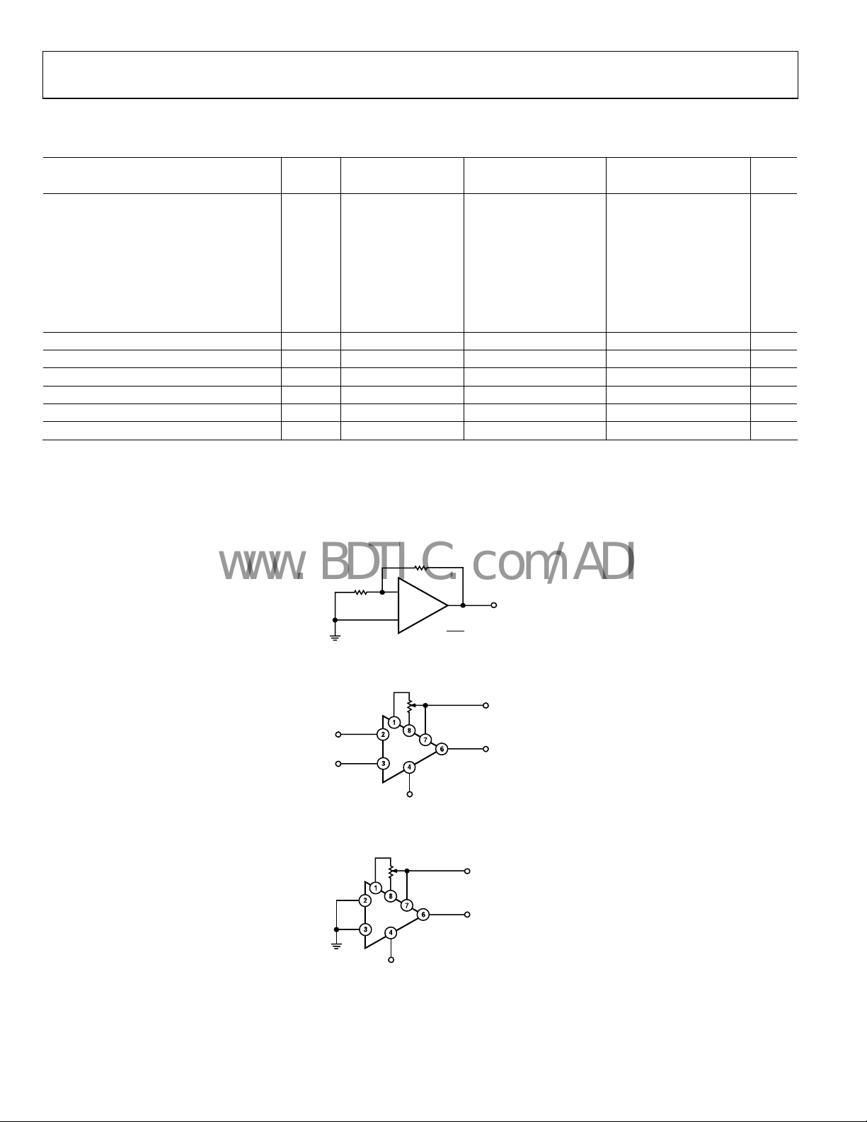
TEST CIRCUITS
50Ω
–
OP177
+
Figure 3. Typical Offset Vo
–
INPUT
+
–
OP177
+
Figure 4. Optional Of
20kΩ
–
OP177
+
200k
V
O
V
=
OS
4000
ltage Test Circuit
20kΩ
V
TRIM RANGE IS
OS
TYPICALLY ±3.0mV
V–
fset Nulling Circuit
+20V
PINOUT S SHOWN FO R
P AND Z PACKAGES
V
O
00289-003
V+
OUTPUT
00289-004
–20V
Figure 5. Burn-In Circuit
Rev. E | Page 4 of 16
0289-005

OP177
www.BDTIC.com/ADI
ABSOLUTE MAXIMUM RATINGS
Table 3.
Parameter Ratings
Supply Voltage ±22 V
Internal Power Dissipation
Differential Input Voltage ±30 V
Input Voltage ±22 V
Output Short-Circuit Duration Indefinite
Storage Temperature Range −65°C to +125°C
Operating Temperature Range −40°C to +85°C
Lead Temperature (Soldering, 60 sec) 300°C
DICE Junction Temperature (TJ) −65°C to +150°C
1
For supply voltages less than ±22 V, the absolute maximum input voltage is
equal to the supply voltage.
1
500 mW
ESD CAUTION
ESD (electrostatic discharge) sensitive device. Electrostatic charges as high as 4000 V readily accumulate on
the human body and test equipment and can discharge without detection. Although this product features
proprietary ESD protection circuitry, permanent damage may occur on devices subjected to high energy
electrostatic discharges. Therefore, proper ESD precautions are recommended to avoid performance
degradation or loss of functionality.
Stresses above those listed under Absolute Maximum Ratings
may cause permanent damage to the device. This is a stress
rating only; functional operation of the device at these or any
other conditions above those indicated in the operational
section of this specification is not implied. Exposure to absolute
maximum rating conditions for extended periods may affect
device reliability.
THERMAL RESISTANCE
θJA is specified for worst-case mounting conditions, that is, θJA
is specified for device in socket for PDIP; θ
device soldered to printed circuit board for SOIC package.
Table 4. Thermal Resistance
Package Type θ
8-Lead PDIP (P-Suffix) 103 43 °C/W
8-Lead SOIC (S-Suffix) 158 43 °C/W
is specified for
JA
JA
θ
Unit
JC
Rev. E | Page 5 of 16
 Loading...