Analog Devices OP177 Datasheet

Ultraprecision
NC = NO CONNECT
a
FEATURES
Ultralow Offset Voltage:
TA = +258C: 10 mV max
–558C ≤ T
Outstanding Offset Voltage Drift: 0.1 mV/8C max
Excellent Open-Loop Gain and Gain Linearity:
12 V/mV typ
CMRR: 130 dB min
PSRR: 120 dB min
Low Supply Current: 2.0 mA max
Fits Industry Standard Precision Op Amp Sockets
(OP07/OP77)
GENERAL DESCRIPTION
The OP177 features the highest precision performance of any
op amp currently available. Offset voltage of the OP177 is only
10 µV max at room temperature and 20 µV max over the full
military temperature range of –55°C to +125°C. The ultralow
V
of the OP177, combines with its exceptional offset voltage
OS
drift (TCV
external V
temperature.
The OP177’s open-loop gain of 12 V/µV is maintained over the
full ±10 V output range. CMRR of 130 dB min, PSRR of
120 dB min, and maximum supply current of 2 mA are just a
few examples of the excellent performance of this operational
amplifier. The OP177’s combination of outstanding specifications
insure accurate performance in high closed-loop gain applications.
≤ +1258C: 20 mV max
A
) of 0.1 µV/°C max, to eliminate the need for
OS
adjustment and increases system accuracy over
OS
Operational Amplifier
OP177
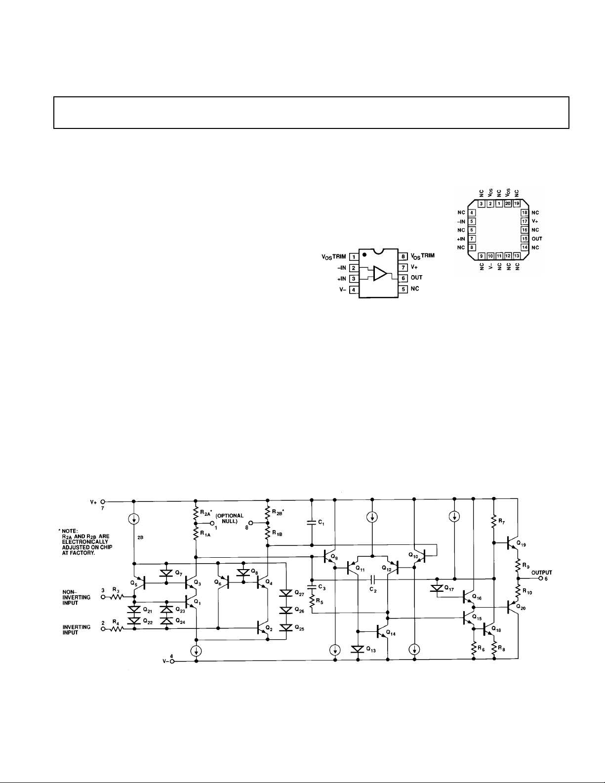
PIN CONNECTIONS
Epoxy Mini-DIP
(P Suffix)
8-Pin Hermetic DIP
(Z-Suffix)
8-Pin SO
(S-Suffix)
NC = NO CONNECT
This low noise bipolar input op amp is also a cost effective
alternative to chopper-stabilized amplifiers. The OP177 provides
chopper-type performance without the usual problems of high
noise, low frequency chopper spikes, large physical size, limited
common-mode input voltage range, and bulky external storage
capacitors.
The OP177 is offered in both the –55°C to +125°C military,
and the –40°C to +85°C extended industrial temperature
ranges. This product is available in 8-pin ceramic and epoxy
DIPs, as well as the space saving 8-pin Small-Outline (SO) and
the Leadless Chip Carrier (LCC) packages.
OP177BRC/883
LCC (RC Suffix)
REV. B
Information furnished by Analog Devices is believed to be accurate and
reliable. However, no responsibility is assumed by Analog Devices for its
use, nor for any infringements of patents or other rights of third parties
which may result from its use. No license is granted by implication or
otherwise under any patent or patent rights of Analog Devices.
Figure 1. Simplified Schematic
© Analog Devices, Inc., 1995
One Technology Way, P.O. Box 9106, Norwood, MA 02062-9106, U.S.A.
Tel: 617/329-4700 Fax: 617/326-8703

OP177–SPECIFICATIONS
ELECTRICAL CHARACTERISTICS
(@ VS = 615 V, TA = +258C, unless otherwise noted)
OP177A OP177B
Parameter Symbol Conditions Min Typ Max Min Typ Max Units
Input Offset Voltage V
Long-Term Input Offset Voltage Stability ∆V
Input Offset Current I
Input Bias Current I
Input Noise Voltage e
Input Noise Current i
n
Input Resistance Differential-Mode R
Input Resistance Common-Mode R
OS
/Time (Note 1) 0.2 0.2 µV/Mo
OS
OS
B
n
IN
INCM
fo = 1 Hz to 100 Hz
fo = 1 Hz to 100 Hz
(Note 3) 26 45 26 45 MΩ
–0.2 1.5 –0.2 2.0 nA
2
2
410 1025µV
0.3 1.0 0.3 1.5 nA
118 150 118 150 nV rms
38 38pA
rms
200 200 GΩ
Input Voltage Range IVR (Note 4) ±13 ± 14 ±13 ±14 V
Common-Mode Rejection Ratio CMRR V
Power Supply Rejection Ratio PSRR V
Large Signal Voltage Gain A
Output Voltage Swing V
VO
O
Slew Rate SR R
Closed-Loop Bandwidth BW A
Open-Loop Output Resistance R
Power Consumption P
Supply Current I
O
D
SY
Offset Adjustment Range Rp = 20 kΩ
NOTES
1
Long-Term Input Offset Voltage Stability refers to the averaged trend line of VOS vs. Time over extended periods after the first 30 days of operation. Excluding the
initial hour of operation, changes in VOS during the first 30 operating days are typically less than 2.0 µV.
2
Sample tested.
3
Guaranteed by design.
4
Guaranteed by CMRR test condition.
5
To insure high open-loop gain throughout the ±10 V output range, AVO is tested at –10 V ≤ VO ≤ 0 V, 0 V ≤ VO ≤ +10 V, and –10 V ≤ VO ≤ +10 V.
Specifications subject to change without notice.
= ±13 V 130 140 130 140 dB
CM
= ±3 V to ±18 V 120 125 115 125 dB
S
RL ≥ 2 kΩ, VO = ±10 V55000 12000 5000 12000 V/mV
RL ≥ 10 kΩ±13.5 ±14.0 ±13.5 ±14.0 V
≥ 2 kΩ±12.5 ±13.0 ±12.5 ±13.0 V
R
L
≥ 1 kΩ±12.0 ±12.5 ±12.0 ±12.5 V
R
L
L
VCL
≥ 2 kΩ
= +1
2
2
0.1 0.3 0.1 0.3 V/µs
0.4 0.6 0.4 0.6 MHz
60 60 Ω
VS = ±15 V, No Load 50 60 50 60 mW
= ±3 V, No Load 3.5 4.5 3.5 4.5 mW
V
S
VS = ±15 V, No Load 1.6 2.0 1.6 2.0 mA
±3 ±3mV
ELECTRICAL CHARACTERISTICS
(@ VS = 615 V, –55°C ≤ TA ≤ +1258C, unless otherwise noted)
OP177A OP177B
Parameter Symbol Conditions Min Typ Max Min Typ Max Units
Input Offset Voltage V
OS
Average Input Offset Voltage Drift TCV
Input Offset Current I
OS
Average Input Offset Current Drift TCI
Input Bias Current I
B
Average Input Bias Current Drift TCI
OS
B
OS
(Note 1) 0.03 0.1 0.1 0.3 µV/°C
(Note 2) 1.5 25 1.5 25 pA/°C
–0.2 2.4 4 –0.2 2.4 4 nA
(Note 2) 8 25 8 25 pA/°C
10 20 25 55 µV
0.5 1.5 0.5 2.0 nA
Input Voltage Range IVR (Note 3) ±13 ±13.5 ±13 ±13.5 V
Common-Mode Rejection Ratio CMRR V
Power Supply Rejection Ratio PSRR V
Large-Signal Voltage Gain A
Output Voltage Swing V
Power Consumption P
Supply Current I
NOTES
1
TCVOS is 100% tested.
2
Guaranteed by endpoint limits.
3
Guaranteed by CMRR test condition.
4
To insure high open-loop gain throughout the ±10 V output range, AVO is tested at –10 V ≤ VO ≤ 0 V, 0 V ≤ VO ≤ +10 V, and –10 V ≤ VO ≤ +10 V.
Specifications subject to change without notice.
VO
O
D
SY
= ±13 V 120 140 120 140 dB
CM
= ±3 V to ±18 V 120 125 110 120 dB
S
RL ≥ 2 kΩ, VO = ±10 V42000 6000 2000 6000 V/mV
RL ≥ 2 kΩ±12 ±13.0 ±12 ±13.0 V
VS = ±15 V, No Load 60 75 60 75 mW
VS = ±15 V, No Load 2.0 2.5 2.0 2.5 mA
–2–
REV. B

ELECTRICAL CHARACTERISTICS
(@ VS = 615 V, TA = +258C, unless otherwise noted)
OP177
Parameter Symbol Conditions Min Typ Max Min Typ Max Min Typ Max Units
OP177E OP177F OP177G
Input Offset Voltage V
OS
41010252060µV
Long-Term Input Offset
Voltage Stability ∆VOS/Time (Note 1) 0.2 0.3 0.4 µV/Mo
Input Offset Current I
Input Bias Current I
Input Noise Voltage e
Input Noise Current i
OS
B
n
n
fo = 1 Hz to 100 Hz
fo = 1 Hz to 100 Hz
2
2
0.3 1.0 0.3 1.5 0.3 2.8 nA
–0.2 1.0 1.5 –0.2 1.2 2.0 –0.2 1.2 2.8 nA
118 150 118 150 118 150 nV rms
38 38 38pA
rms
Input Resistance
Differential-Mode R
IN
(Note 3) 26 45 26 45 18.5 45 MΩ
Input Resistance
Common-Mode R
INCM
200 200 200 GΩ
Input Voltage Range IVR (Note 4) ± 13 ±14 ±13 ±14 ±13 ±14 V
Common-Mode
Rejection Ratio CMRR VCM = ±13 V 130 140 130 140 115 140 dB
Power Supply
Rejection Ratio PSRR VS = ±3 V to ±18 V 120 125 115 125 110 120 dB
Large Signal RL ≥ 2 kΩ,
Voltage Gain A
VO
VO = ±10 V
5
5000 12000 5000 12000 2000 6000 V/mV
Output Voltage
Swing V
O
RL ≥ 10 kΩ±13.5 ±14.0 ±13.5 ±14.0 ± 13.5 ±14.0 V
RL ≥ 2 kΩ±12.5 ±13.0 ±12.5 ±13.0 ± 12.5 ±13.0 V
Slew Rate SR RL ≥ 2 kΩ
RL ≥ 1 kΩ±12.0 ±12.5 ±12.0 ±12.5 ± 12.0 ±12.5 V
Closed-Loop
Bandwidth BW A
VCL
= +1
2
2
0.1 0.3 0.1 0.3 0.1 0.3 V/µs
0.4 0.6 0.4 0.6 0.4 0.6 MHz
Open-Loop Output
Resistance R
Power Consumption P
O
D
VS = ±15 V, No Load 50 60 50 60 50 60 mW
60 60 60 Ω
VS = ±3 V, No Load 3.5 4.5 3.5 4.5 3.5 4.5 mW
Supply Current I
SY
VS = ±15 V, No Load 1.6 2.0 1.6 2.0 1.6 2.0 mA
Offset Adjustment
Range RP = 20 kΩ±3 ±3 ±3mV
NOTES
1
Long-Term Input Offset Voltage Stability refers to the averaged trend line of VOS vs. time over extended periods after the first 30 days of operation. Excluding the initial hour of operation, changes in VOS during the first 30 operating days are typically less than 2.0 µV.
2
Sample tested.
3
Guaranteed by design.
4
Guaranteed by CMRR test condition.
5
To insure high open-loop gain throughout the ±10 V output range, AVO is tested at –10 V ≤ VO ≤ 0 V, 0 V ≤ VO ≤ +10 V, and –10 V ≤ VO ≤ +10 V.
Specifications subject to change without notice.
REV. B
–3–

OP177–SPECIFICATIONS
ELECTRICAL CHARACTERISTICS
(@ VS = 615 V, –40°C ≤ TA ≤ +858C, unless otherwise noted)
OP177E OP177F OP177G
Parameter Symbol Conditions Min Typ Max Min Typ Max Min Typ Max Units
Input Offset Voltage V
OS
10 20 15 40 20 100 µV
Average Input Offset
Voltage Drift TCV
Input Offset Current I
OS
(Note 1) 0.03 0.1 0.1 0.3 0.7 1.2 µV/°C
OS
0.5 1.5 0.5 2.2 0.5 4.5 nA
Average Input Offset
Current Drift TCI
Input Bias Current I
B
(Note 2) 1.5 25 1.5 40 1.5 85 pA/°C
OS
–0.2 2.4 4 –0.2 2.4 4 2.4 ±6.0 nA
Average Input Bias
Current Drift TCI
(Note 2) 8 25 8 40 15 60 pA/°C
B
Input Voltage Range IVR (Note 3) ±13 ± 13.5 ±13 ± 13.5 ±13.0 ±13.5 V
Common-Mode
Rejection Ratio CMRR VCM = ±13 V 120 140 120 140 110 140 dB
Power Supply Rejection
Ratio PSRR VS = ±3 V to ±18 V 120 125 110 120 106 115 dB
Large-Signal
Voltage Gain A
Output Voltage Swing V
Power Consumption P
Supply Current I
NOTES
1
OP177E: TCVOS is 100% tested.
2
Guaranteed by endpoint limits.
3
Guaranteed by CMRR test condition.
4
To insure high open-loop gain throughout the ±10 V output range, AVO is tested at –10 V ≤ VO ≤ 0 V, 0 V ≤ VO ≤ +10 V, and –10 V ≤ VO ≤ +10 V.
Specifications subject to change without notice.
VO
O
D
SY
RL ≥ 2 kΩ, VO = ±10 V42000 6000 2000 6000 1000 4000 V/mV
RL ≥ 2 kΩ±12 ±13.0 ±12 ±13.0 ±12.0 ±13.0 V
VS = ±15 V, No Load 60 75 60 75 60 75 mW
VS = ±15 V, No Load 2.0 2.5 2.0 2.5 2.0 2.5
mA
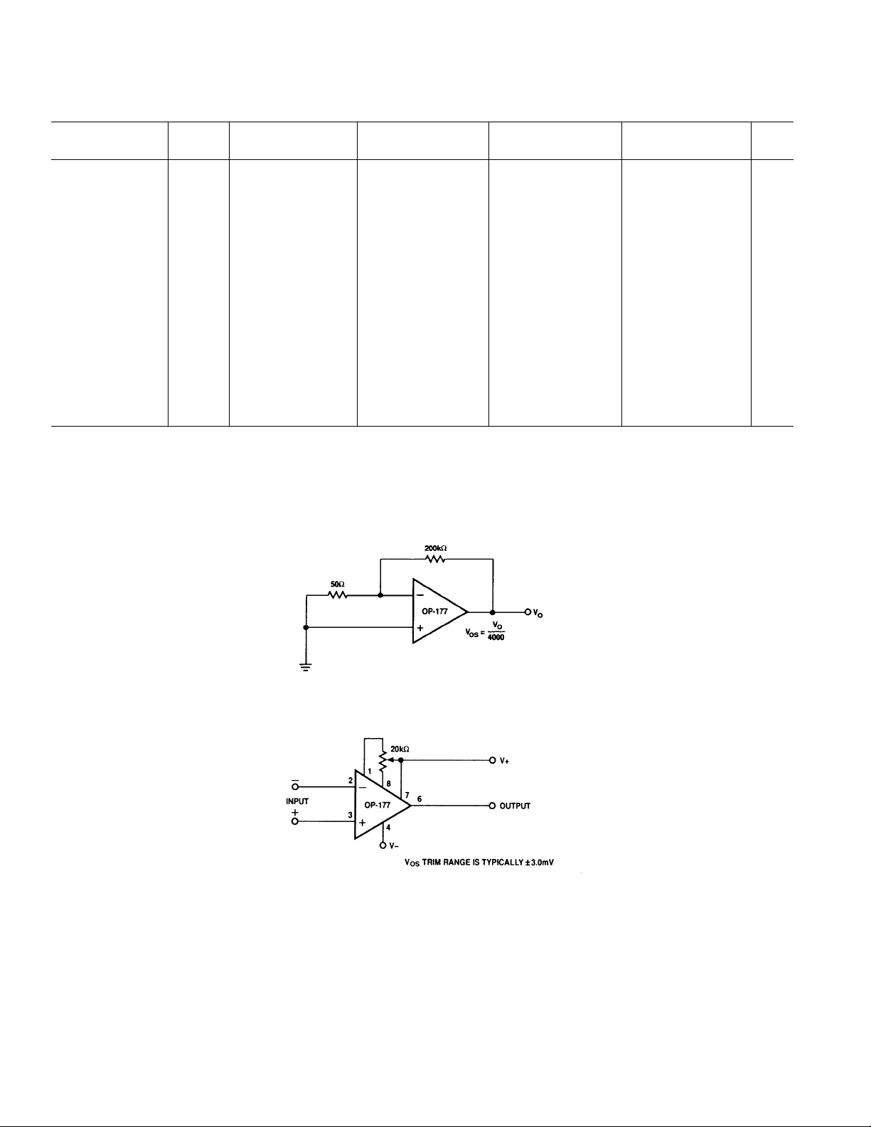
Figure 2. Typical Offset Voltage Test Circuit
Figure 3. Optional Offset Nulling Circuit
REV. B–4–
 Loading...