Precision Low Noise, Low Input
–
+
FEATURES
Low offset voltage: 60 μV maximum
Very low offset voltage drift: 0.7 μV/°C maximum
Low input bias current: 2 nA maximum
Low noise: 8 nV/√Hz typical
CMRR, PSRR, and A
Low supply current: 400 μA per amplifier
Dual supply operation: ±2.5 V to ±15 V
Unity-gain stable
No phase reversal
Inputs internally protected beyond supply voltage
APPLICATIONS
Wireless base station control circuits
Optical network control circuits
Instrumentation
Sensors and controls
Thermocouples
Resistor thermal detectors (RTDs)
Strain bridges
Shunt current measurements
Precision filters
> 120 dB minimum
VO
Bias Current Operational Amplifiers
OP1177/OP2177/OP4177
PIN CONFIGURATIONS
NC
1
IN
2
18
NC
–IN
OP1177
+IN
V–
45
NC = NO CONNECT
NC
V+
OUT
NC
02627-001
OP1177
IN
3
V–
4
NC = NO CONNECT
Figure 1. 8-Lead MSOP (RM Suffix) Figure 2. 8-Lead SOIC_N (R Suffix)
OUT A
1
–IN A
2
OUT A
–IN A
+IN A
18
OP2177
45
V–
V+
OUT B
–IN B
+IN B
02627-003
+IN A
OP2177
3
V–
4
Figure 3. 8-Lead MSOP (RM Suffix) Figure 4. 8-Lead SOIC_N (R Suffix)
OUT A
1
213
–IN A
+IN A
3
OP4177
V+
4
5
+IN B
69
–IN B
78
OUT B
OUT D
14
–IN D
+IN D
12
11
V–
+IN C
10
–IN C
OUT C
OUT A
OUT B
02627-005
–IN A
+IN A
+IN B
–IN B
1
OP4177
V+
7
Figure 5. 14-Lead SOIC_N (R Suffix) Figure 6. 14-Lead TSSOP (RU Suffix)
NC
8
V+
7
OUT
6
NC
5
02627-002
V+
8
OUT B
7
–IN B
6
+IN B
5
OUT D
14
–IN D
+IN D
V–
+IN C
–IN C
8
OUT C
02627-004
02627-006
GENERAL DESCRIPTION
The OPx177 family consists of very high precision, single, dual,
and quad amplifiers featuring extremely low offset voltage and
drift, low input bias current, low noise, and low power consumption. Outputs are stable with capacitive loads of over 1000 pF
with no external compensation. Supply current is less than 500 A
per amplifier at 30 V. Internal 500 series resistors protect the
inputs, allowing input signal levels several volts beyond either
supply without phase reversal.
Unlike previous high voltage amplifiers with very low offset
voltages, the OP1177 (single) and OP2177 (dual) amplifiers
are available in tiny 8-lead surface-mount MSOP and 8-lead
narrow SOIC packages. The OP4177 (quad) is available in
TSSOP and 14-lead narrow SOIC packages. Moreover, specified
performance in the MSOP and the TSSOP is identical to
Rev. G
Information furnished by Analog Devices is believed to be accurate and reliable. However, no
responsibility is assumed by Analog Devices for its use, nor for any infringements of patents or other
rights of third parties that may result from its use. Specifications subject to change without notice. No
license is granted by implication or otherwise under any patent or patent rights of Analog Devices.
Trademarks and registered trademarks are the property of their respective owners.
performance in the SOIC package. MSOP and TSSOP are
available in tape and reel only.
The OPx177 family offers the widest specified temperature
range of any high precision amplifier in surface-mount packaging.
All versions are fully specified for operation from −40°C to
+125°C for the most demanding operating environments.
Applications for these amplifiers include precision diode
power measurement, voltage and current level setting, and
level detection in optical and wireless transmission systems.
Additional applications include line-powered and portable
instrumentation and controls—thermocouple, RTD, strainbridge, and other sensor signal conditioning—and precision filters.
One Technology Way, P.O. Box 9106, Norwood, MA 02062-9106, U.S.A.
Tel: 781.329.4700 www.analog.com
Fax: 781.461.3113 ©2001–2009 Analog Devices, Inc. All rights reserved.

OP1177/OP2177/OP4177
TABLE OF CONTENTS
Features .............................................................................................. 1
Overload Recovery Time .......................................................... 15
Applications ....................................................................................... 1
Pin Configurations ........................................................................... 1
General Description ......................................................................... 1
Revision History ............................................................................... 2
Specifications ..................................................................................... 3
Electrical Characteristics ............................................................. 4
Absolute Maximum Ratings ............................................................ 5
Thermal Resistance ...................................................................... 5
ESD Caution .................................................................................. 5
Typical Performance Characteristics ............................................. 6
Functional Description .................................................................. 14
Total Noise-Including Source Resistors ................................... 14
Gain Linearity ............................................................................. 14
Input Overvoltage Protection ................................................... 15
Output Phase Reversal ............................................................... 15
THD + Noise ............................................................................... 16
Capacitive Load Drive ............................................................... 16
Stray Input Capacitance Compensation .................................. 17
Reducing Electromagnetic Interference .................................. 17
Proper Board Layout .................................................................. 18
Difference Amplifiers ................................................................ 18
A High Accuracy Thermocouple Amplifier ........................... 19
Low Power Linearized RTD ...................................................... 19
Single Operational Amplifier Bridge ....................................... 20
Realization of Active Filters .......................................................... 21
Band-Pass KRC or Sallen-Key Filter ........................................ 21
Channel Separation .................................................................... 21
References on Noise Dynamics and Flicker Noise ............... 21
Outline Dimensions ....................................................................... 22
Ordering Guide .......................................................................... 24
Settling Time ............................................................................... 15
REVISION HISTORY
11/09—Rev. F to Rev. G
Changes to Figure 64 ...................................................................... 19
Changes to Ordering Guide .......................................................... 24
Updated Outline Dimensions ....................................................... 22
5/09—Rev. E to Rev. F
Changes to Figure 64 ...................................................................... 19
Changes to Ordering Guide .......................................................... 24
10/07—Rev. D to Rev. E
Changes to General Description .................................................... 1
Changes to Table 4 ............................................................................ 5
Updated Outline Dimensions ....................................................... 22
7/06—Rev. C to Rev. D
Changes to Table 4 ............................................................................ 5
Changes to Figure 51 ...................................................................... 14
Changes to Figure 52 ...................................................................... 15
Changes to Figure 54 ...................................................................... 16
Changes to Figure 58 to Figure 61 ................................................ 17
Changes to Figure 62 and Figure 63 ............................................. 18
Changes to Figure 64 ...................................................................... 19
Changes to Figure 65 and Figure 66 ............................................. 20
Rev. G | Page 2 of 24
Changes to Figure 67 and Figure 68............................................. 21
Removed SPICE Model Section ................................................... 21
Updated Outline Dimensions ....................................................... 22
Changes to Ordering Guide .......................................................... 24
4/04—Rev. B to Rev. C
Changes to Ordering Guide ............................................................. 4
Changes to TPC 6 .............................................................................. 5
Changes to TPC 26 ............................................................................ 7
Updated Outline Dimensions ....................................................... 17
4/02—Rev. A to Rev. B
Added OP4177 ......................................................................... Global
Edits to Specifications ....................................................................... 2
Edits to Electrical Characteristics Headings .................................. 4
Edits to Ordering Guide ................................................................... 4
11/01—Rev. 0 to Rev. A
Edit to Features .................................................................................. 1
Edits to TPC 6 ................................................................................... 5
7/01—Revision 0: Initial Version

OP1177/OP2177/OP4177
SPECIFICATIONS
ELECTRICAL CHARACTERISTICS
VS = ±5.0 V, VCM = 0 V, TA = 25°C, unless otherwise noted.
Table 1.
Parameter Symbol Conditions Min Typ1 Max Unit
INPUT CHARACTERISTICS
Offset Voltage
OP1177 VOS 15 60 V
OP2177/OP4177 VOS 15 75 V
OP1177/OP2177 VOS −40°C < TA < +125°C 25 100 V
OP4177 VOS −40°C < TA < +125°C 25 120 V
Input Bias Current IB −40°C < TA < +125°C −2 +0.5 +2 nA
Input Offset Current IOS −40°C < TA < +125°C −1 +0.2 +1 nA
Input Voltage Range −3.5 +3.5 V
Common-Mode Rejection Ratio CMRR VCM = −3.5 V to +3.5 V 120 126 dB
−40°C < TA < +125°C 118 125 dB
Large Signal Voltage Gain AVO R
Offset Voltage Drift
OP1177/OP2177 ∆VOS/∆T −40°C < TA < +125°C 0.2 0.7 V/°C
OP4177 ∆VOS/∆T −40°C < TA < +125°C 0.3 0.9 V/°C
OUTPUT CHARACTERISTICS
Output Voltage High VOH I
Output Voltage Low VOL I
Output Current I
V
OUT
POWER SUPPLY
Power Supply Rejection Ratio
OP1177 PSRR VS = ±2.5 V to ±15 V 120 130 dB
−40°C < TA < +125°C 115 125 dB
OP2177/OP4177 PSRR VS = ±2.5 V to ±15 V 118 121 dB
−40°C < TA < +125°C 114 120 dB
Supply Current per Amplifier ISY V
−40°C < TA < +125°C 500 600 A
DYNAMIC PERFORMANCE
Slew Rate SR RL = 2 kΩ 0.7 V/s
Gain Bandwidth Product GBP 1.3 MHz
NOISE PERFORMANCE
Voltage Noise en p-p 0.1 Hz to 10 Hz 0.4 V p-p
Voltage Noise Density en f = 1 kHz 7.9 8.5 nV/√Hz
Current Noise Density in f = 1 kHz 0.2 pA/√Hz
MULTIPLE AMPLIFIERS CHANNEL SEPARATION CS DC 0.01 V/V
f = 100 kHz −120 dB
1
Typical values cover all parts within one standard deviation of the average value. Average values given in many competitor data sheets as typical give unrealistically
low estimates for parameters that can have both positive and negative values.
= 2 kΩ, VO = −3.5 V to +3.5 V 1000 2000 V/mV
L
= 1 mA, −40°C < TA < +125°C +4 +4.1 V
L
= 1 mA, −40°C < TA < +125°C −4.1 −4 V
L
< 1.2 V ±10 mA
DROPOUT
= 0 V 400 500 A
O
Rev. G | Page 3 of 24

OP1177/OP2177/OP4177
ELECTRICAL CHARACTERISTICS
VS = ±15 V, VCM = 0 V, TA = 25°C, unless otherwise noted.
Table 2.
Parameter Symbol Conditions Min Typ1 Max Unit
INPUT CHARACTERISTICS
Offset Voltage
OP1177 VOS 15 60 V
OP2177/OP4177 VOS 15 75 V
OP1177/OP2177 VOS −40°C < TA < +125°C 25 100 V
OP4177 VOS −40°C < TA < +125°C 25 120 V
Input Bias Current IB −40°C < TA < +125°C −2 +0.5 +2 nA
Input Offset Current IOS −40°C < TA < +125°C −1 +0.2 +1 nA
Input Voltage Range −13.5 +13.5 V
Common-Mode Rejection Ratio CMRR VCM = −13.5 V to +13.5 V,
−40°C < TA < +125°C 120 125 dB
Large Signal Voltage Gain AVO R
Offset Voltage Drift
OP1177/OP2177 ∆VOS/∆T −40°C < TA < +125°C 0.2 0.7 V/°C
OP4177 ∆VOS/∆T −40°C < TA < +125°C 0.3 0.9 V/°C
OUTPUT CHARACTERISTICS
Output Voltage High VOH I
Output Voltage Low VOL I
Output Current I
V
OUT
Short-Circuit Current ISC ±25 mA
POWER SUPPLY
Power Supply Rejection Ratio
OP1177 PSRR VS = ±2.5 V to ±15 V 120 130 dB
−40°C < TA < +125°C 115 125 dB
OP2177/OP4177 PSRR VS = ±2.5 V to ±15 V 118 121 dB
−40°C < TA < +125°C 114 120 dB
Supply Current per Amplifier ISY V
−40°C < TA < +125°C 500 600 A
DYNAMIC PERFORMANCE
Slew Rate SR RL = 2 kΩ 0.7 V/s
Gain Bandwidth Product GBP 1.3 MHz
NOISE PERFORMANCE
Voltage Noise en p-p 0.1 Hz to 10 Hz 0.4 V p-p
Voltage Noise Density en f = 1 kHz 7.9 8.5 nV/√Hz
Current Noise Density in f = 1 kHz 0.2 pA/√Hz
MULTIPLE AMPLIFIERS CHANNEL SEPARATION CS DC 0.01 V/V
f = 100 kHz −120 dB
1
Typical values cover all parts within one standard deviation of the average value. Average values given in many competitor data sheets as typical give unrealistically
low estimates for parameters that can have both positive and negative values.
= 2 kΩ, VO = –13.5 V to +13.5 V 1000 3000 V/mV
L
= 1 mA, −40°C < TA < +125°C +14 +14.1 V
L
= 1 mA, −40°C < TA < +125°C −14.1 −14 V
L
< 1.2 V ±10 mA
DROPOUT
= 0 V 400 500 A
O
Rev. G | Page 4 of 24

OP1177/OP2177/OP4177
ABSOLUTE MAXIMUM RATINGS
Table 3.
Parameter Rating
Supply Voltage 36 V
Input Voltage VS− to VS+
Differential Input Voltage ±Supply Voltage
Storage Temperature Range
R, RM, and RU Packages −65°C to +150°C
Operating Temperature Range
OP1177/OP2177/OP4177 −40°C to +125°C
Junction Temperature Range
R, RM, and RU Packages −65°C to +150°C
Lead Temperature, Soldering (10 sec) 300°C
Stresses above those listed under Absolute Maximum Ratings
may cause permanent damage to the device. This is a stress
rating only; functional operation of the device at these or any
other conditions above those indicated in the operational
section of this specification is not implied. Exposure to absolute
maximum rating conditions for extended periods may affect
device reliability.
THERMAL RESISTANCE
θJA is specified for the worst-case conditions, that is, a device
soldered in a circuit board for surface-mount packages.
Table 4. Thermal Resistance
Package Type θJA θ
8-Lead MSOP (RM-8)1 190 44 °C/W
8-Lead SOIC_N (R-8) 158 43 °C/W
14-Lead SOIC_N (R-14) 120 36 °C/W
14-Lead TSSOP (RU-14) 240 43 °C/W
1
MSOP is available in tape and reel only.
Unit
JC
ESD CAUTION
Rev. G | Page 5 of 24

OP1177/OP2177/OP4177
TYPICAL PERFORMANCE CHARACTERISTICS
50
VSY = ±15V
45
40
35
30
25
20
15
NUMBER OF AMPLIFIERS
10
5
0
–30 –20 –10 0 10 20 30 40
–40
INPUT OFFSET VOLTAGE (µV)
Figure 7. Input Offset Voltage Distribution
02627-007
1.8
VSY = ±15V
= 25°C
T
A
1.6
1.4
1.2
1.0
0.8
0.6
ΔOUTPUT VOL TAGE (V)
0.4
0.2
0
0.001 10
SOURCE
SINK
0.01 0.1 1
LOAD CURRENT (mA)
Figure 10. Output Voltage to Supply Rail vs. Load Current
02627-010
90
80
70
60
50
40
30
NUMBER OF AMPLIFIERS
20
10
0
0.15 0.25 0.35 0.45 0. 55 0.65
0.05
INPUT OFFSET VOLTAGE DRIFT (µV/°C)
Figure 8. Input Offset Voltage Drift Distribution
VSY = ±15V
02627-008
140
VSY = ±15V
120
100
80
60
40
NUMBER OF AMPL IFIERS
20
0
0.1 0.2 0.3 0.4 0.5 0.6 0.7
0
INPUT BIAS CURRENT (nA)
Figure 9. Input Bias Current Distribution
02627-009
3
2
1
0
–1
INPUT BI AS CURRE NT (nA)
–2
–3
–50 150
0 50 100
TEMPERATURE (°C)
Figure 11. Input Bias Current vs. Temperature
60
VSY = ±15V
C
= 0
L
50
R
=
∞
L
40
30
GAIN
20
10
OPEN-LOOP GAIN (dB)
0
–10
–20
100k 10M
1M
FREQUENCY (Hz)
Figure 12. Open-Loop Gain and Phase Shift vs. Frequency
PHASE
VSY = ±15V
270
225
180
135
90
45
0
–45
–90
2627-011
PHASE SHIFT (Degrees)
02627-012
Rev. G | Page 6 of 24

OP1177/OP2177/OP4177
V
120
100
80
60
AV = 100
40
AV = 10
20
0
AV = 1
–20
CLOSED-LOOP GAIN (dB)
–40
–60
–80
1k 100M
10k 100k 1M 10M
FREQUENCY (Hz)
VSY = ±15V
V
= 4mV p-p
IN
C
= 0
L
R
=
∞
L
Figure 13. Closed-Loop Gain vs. Frequency
02627-013
VOLTAGE (100mV/DIV)
GND
VSY = ±15V
= 1,000pF
C
L
= 2kΩ
R
L
= 100mV
V
IN
= 1
A
V
TIME (100µ s/DIV)
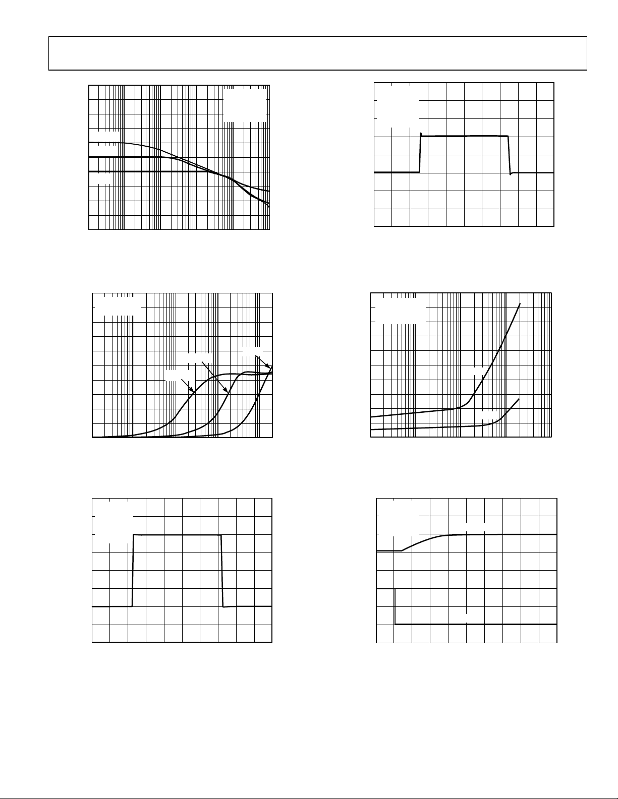
Figure 16. Small Signal Transient Response
02627-016
500
VSY = ±15V
450
= 50mV p-p
V
IN
400
350
300
250
200
150
OUTPUT IMPEDANCE (Ω)
100
50
0
100
1k 10k 100k 1M
FREQUENCY (Hz)
AV = 10
AV = 100
AV = 1
2627-014
Figure 14. Output Impedance vs. Frequency
VSY = ±15V
C
= 300pF
L
R
= 2kΩ
L
V
= 4V
IN
A
= 1
V
50
VSY = ±15V
45
= 2kΩ
R
L
= 100mV p-p
V
IN
40
35
30
25
20
15
10
SMALL SIG NAL OVERSHO OT (%)
5
0
1 10k
10 100 1k
CAPACITANCE (pF)
+OS
–OS
02627-017
Figure 17. Small Signal Overshoot vs. Load Capacitance
VSY = ±15V
R
= 10kΩ
L
A
= –100
–15V
V
V
= 200mV
IN
0V
OUTPUT
VOLTAGE (1V/DIV)
GND
TIME (100µs/ DIV)
Figure 15. Large Signal Transient Response
02627-015
+200m
0V
TIME (10µs/DIV)
Figure 18. Positive Overvoltage Recovery
INPUT
2627-018
Rev. G | Page 7 of 24

OP1177/OP2177/OP4177
–
V
√
OUTPUT
15V
0V
VSY = ±15V
R
= 10kΩ
L
A
= –100
V
V
= 200mV
IN
0V
VSY = ±15V
(0.2µV/DIV)
NOISE
V
200m
CMRR (dB)
PSRR (dB)
INPUT
TIME (4µs/DIV)
Figure 19. Negative Overvoltage Recovery
140
120
100
80
60
40
20
0
10 10M
100 1k 10k 100k 1M
FREQUENCY (Hz)
VSY = ±15V
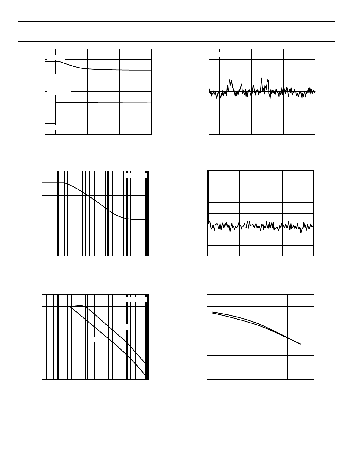
Figure 20. CMRR vs. Frequency
140
120
100
80
60
+PSRR
VSY = ±15V
–PSRR
2627-019
TIME (1s/DIV)
2627-022
Figure 22. 0.1 Hz to 10 Hz Input Voltage Noise
18
VSY = ±15V
16
Hz)
14
12
10
8
6
VOLTAGE NOISE DENSITY (nV/
4
2
2627-020
50 100 150 2000 250
FREQUENCY ( Hz)
02627-023
Figure 23. Voltage Noise Density vs. Frequency
35
30
+I
25
20
15
SC
–I
SC
V
SY
= ±15V
40
20
0
10 10M
100 1k 10k 100k 1M
FREQUENCY (Hz)
Figure 21. PSRR vs. Frequency
02627-021
10
SHORT-CIRCUIT CURRENT (mA)
5
0
–50 150
0 50 100
TEMPERATURE ( °C)
Figure 24. Short-Circuit Current vs. Temperature
2627-024
Rev. G | Page 8 of 24
 Loading...