

High Speed ADC USB FIFO Evaluation Kit
HSC-ADC-EVALB-SC/HSC-ADC-EVALB-DC
FEATURES
Buffer memory board for capturing digital data
used with high speed ADC evaluation boards
to simplify evaluation
32 kB FIFO depth at 133 MSPS (upgradable)
Measures performance with ADC Analyzer™
Real-time FFT and time domain analysis
Analyzes SNR, SINAD, SFDR, and harmonics
Simple USB port interface (2.0)
Supporting ADCs with serial port interfaces (SPI®)
On-board regulator circuit, no power supply required
6 V, 2 A switching power supply included
Compatible with Windows® 98 (2nd ed.), Windows 2000,
Windows Me, and Windows XP
EQUIPMENT NEEDED
Analog signal source and antialiasing filter
Low jitter clock source
High speed ADC evaluation board and ADC data sheet
PC running Windows 98 (2nd ed.), Windows 2000,
Windows Me, or Windows XP
Latest version of ADC Analyzer
USB 2.0 port recommended (USB 1.1-compatible)
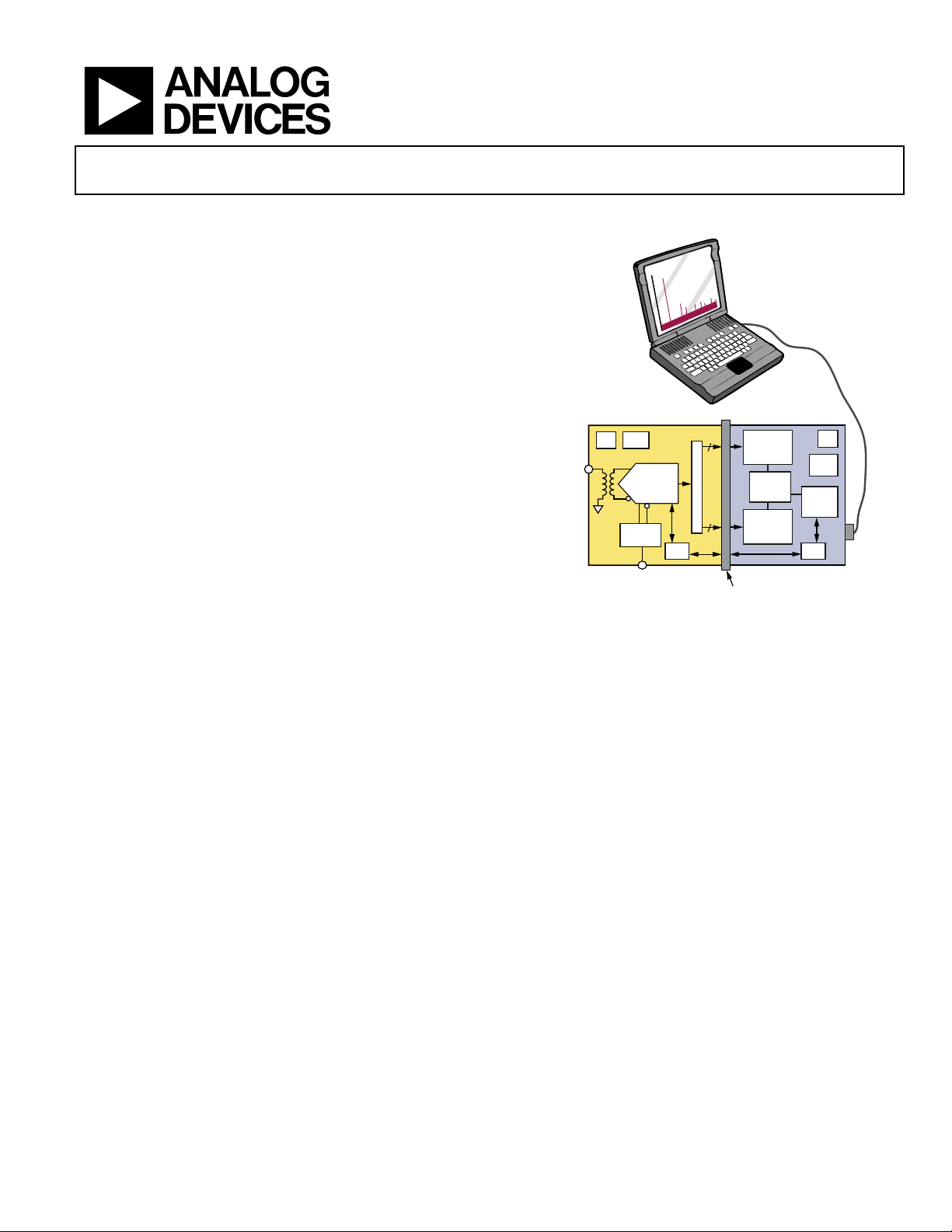
PRODUCT DESCRIPTION
The high speed ADC FIFO evaluation kit includes the latest
version of ADC Analyzer and a buffer memory board to capture
blocks of digital data from the Analog Devices high speed
analog-to-digital converter (ADC) evaluation boards. The FIFO
board is connected to the PC through a USB port and is used
with ADC Analyzer to quickly evaluate the performance of high
speed ADCs. Users can view an FFT for a specific analog input
and encode rate to analyze SNR, SINAD, SFDR, and harmonic
information.
The evaluation kit is easy to set up. Additional equipment needed
includes an Analog Devices high speed ADC evaluation board,
a signal source, and a clock source. Once the kit is connected
and powered, the evaluation is enabled instantly on the PC.
Two versions of the FIFO are available. The HSC-ADC-EVALBDC is used with multichannel ADCs and converters with demultiplexed digital outputs. The HSC-ADC-EVALB-SC evaluation
board is used with single-channel ADCs. See
the FIFO appropriate for your high speed ADC evaluation
board.
Rev. 0
Information furnished by Analog Devices is believed to be accurate and reliable. However, no
responsibility is assumed by Anal og Devices for its use, nor for any infringements of patents or ot her
rights of third parties that may result from its use. Specifications subject to change without notice. No
license is granted by implication or otherwise under any patent or patent rights of Analog Devices.
Trademarks and registered trademarks are the property of their respective owners.
Table 1 to choose
FUNCTIONAL BLOCK DIAGRAM
STANDARD
USB 2.0
HSC-ADC-EVALB-SC
HSC-ADC-EVAL B-DC
CHB FIFO,
32K,
133MHz
TIMING
CIRCUIT
CHA FIFO,
32K,
133MHz
120-PIN CO NNECTOR
OR
+3.0V
REG
USB
CTLR
SPI
FILTERED
ANALOG
INPUT
SINGLE OR DUAL
HIGH-SPEED ADC
EVALUATION BOARD
PS REG
ADC
CLOCK
CIRCUIT
CLOCK INP UT
n
LOGIC
n
SPI
Figure 1.
PRODUCT HIGHLIGHTS
1. Easy to Set Up. Connect the included power supply and
signal sources to the two evaluation boards. Then connect
to the PC and evaluate the performance instantly.
2. ADIsimADC™. ADC Analyzer supports virtual ADC
evaluation using ADI proprietary behavioral modeling
technology. This allows rapid comparison between multiple
ADCs, with or without hardware evaluation boards. For more
information, see AN-737 at
3. USB Port Connection to PC. PC interface is a USB 2.0
connection (1.1-compatible) to the PC. A USB cable is
provided in the kit.
4. 32 kB FIFO. The FIFO stores data from the ADC for processing.
A pin-compatible FIFO family is used for easy upgrading.
5. Up to 133 MSPS Encode Rate on Each Channel. Single-
channel ADCs with encode rates up to 133 MSPS can be used
with the FIFO board. Multichannel and demultiplexed output
ADCs can also be used with the FIFO board with clock rates
up to 266 MSPS.
6. Supports ADC with Serial Port Interface or SPI. Some ADCs
include a feature set that can be changed via the SPI. The FIFO
supports these SPI-driven features through the existing USB
connection to the computer without additional cabling needed.
One Technology Way, P.O. Box 9106, Norwood, MA 02062-9106, U.S.A.
Tel: 781.329.4700 www.analog.com
Fax: 781.461.3113 ©2006 Analog Devices, Inc. All rights reserved.
www.analog.com/ADIsimADC.
PS
05870-001

HSC-ADC-EVALB-SC/HSC-ADC-EVALB-DC
TABLE OF CONTENTS
Features .............................................................................................. 1
Equipment Needed........................................................................... 1
Product Description ......................................................................... 1
Functional Block Diagram .............................................................. 1
Product Highlights........................................................................... 1
Revision History ............................................................................... 2
FIFO Evaluation Board Easy Start.................................................. 3
Requirements ................................................................................ 3
Easy Start Steps ............................................................................. 3
Virtual Evaluation Board Easy Start With ADIsimADC ............ 4
Requirements ................................................................................ 4
Easy Start Steps ............................................................................. 4
FIFO 4.1 Data Capture Board Features ......................................... 5
FIFO 4.1 Supported ADC Evaluation Boards .......................... 6
Theory of Operation ........................................................................ 9
Clocking with Interleaved Data................................................ 10
Connecting to the HSC-ADC-FPGA-4/-8 ............................. 10
Connecting to the DEMUX BRD ............................................ 10
Upgrading FIFO Memory ......................................................... 10
Jumpers ............................................................................................ 11
Default Settings........................................................................... 11
Evaluation Board ............................................................................ 13
Power Supplies ............................................................................ 13
Connection and Setup ............................................................... 13
FIFO Schematics and PCB Layout............................................... 14
Schematics................................................................................... 14
PCB Layout ................................................................................. 21
Bill of Materials ............................................................................... 23
Ordering Information.................................................................... 25
Ordering Guide .......................................................................... 25
Clocking Description................................................................... 9
SPI Description ............................................................................. 9
REVISION HISTORY
2/06—Revision 0: Initial Version
ESD Caution................................................................................ 25
Rev. 0 | Page 2 of 28

HSC-ADC-EVALB-SC/HSC-ADC-EVALB-DC
FIFO EVALUATION BOARD EASY START
REQUIREMENTS
• FIFO evaluation board, ADC Analyzer, and USB cable
• High speed ADC evaluation board and ADC data sheet
• Power supply for ADC evaluation board
• Analog signal source and appropriate filtering
• Low jitter clock source applicable for specific ADC
evaluation, typically <1 ps rms
• PC running Windows 98 (2nd ed.), Windows 2000,
Windows Me, or Windows XP
• PC with a USB 2.0 port recommended (USB 1.1-
compatible)
EASY START STEPS
Note: You need administrative rights for the Windows
operating systems during the entire easy start procedure.
It is recommended to complete every step before reverting
to a normal user mode.
1. Install ADC Analyzer from the CD provided in the FIFO
evaluation kit or download the latest version on the Web.
For the latest updates to the software, check the Analog
Devices website at
2. Connect the FIFO evaluation board to the ADC evaluation
board. If an adapter is required, insert the adapter between
the ADC evaluation board and the FIFO board. If using
the HSC-ADC-EVALB-SC model, connect the evaluation
board to the bottom two rows of the 120-pin connector,
closest to the installed IDT FIFO chip. If using an ADC
with a SPI interface, remove the two 4-pin corner keys so
that the third row can be connected.
3. Connect the provided USB cable to the FIFO evaluation
board and to an available USB port on the computer.
4. Refer to
boards can be used with the default settings.
Table 5 for any jumper changes. Most evaluation
www.analog.com/hsc-FIFO.
6. Once the cable is connected to both the computer and the
FIFO board, and power is supplied, the USB drivers start
to install. To complete the total installation of the FIFO
drivers, you need to complete the new hardware sequence
two times. The first Found New Hardware Wizard opens
with the text message This wizard helps you install
software for…Pre-FIFO 4.1. Click the recommended
install, and go to the next screen. A hardware installation
warning window should then be displayed. Click Continue
Anyway. The next window that opens should finish the PreFIFO 4.1 installation. Click Finish. Your computer should
go through a second Found New Hardware Wizard, and
the text message, This wizard helps you install software
for…Analog Devices FIFO 4.1, should be displayed.
Continue as you did in the previous installation and click
Continue Anyway. Then click Finish on the next two
windows. This completes the installation.
7. (Optional) Verify in the device manager that Analog
Devices, FIFO4.1 is listed under the USB hardware.
8. Apply power to the evaluation board and check the voltage
levels at the board level.
9. Connect the appropriate analog input (which should be
filtered with a band-pass filter) and low jitter clock signal.
Make sure the evaluation boards are powered on before
connecting the analog input and clock.
10. Start ADC Analyzer.
11. Choose an existing configuration file for the ADC
evaluation board or create one.
12. Click Time Data in ADC Analyzer (left-most button under
the menus). A reconstruction of the analog input is
displayed. If the expected signal does not appear, or if there
is only a flat red line, refer to the ADC Analyzer data sheet
at
www.analog.com/hsc-FIFO for more information.
5. After verification, connect the appropriate power supplies
to the ADC evaluation boards. The FIFO evaluation board
is supplied with a wall mount switching power supply that
provides a 6 V, 2 A maximum output. Connect the supply
end to the rated 100 ac to 240 ac wall outlet at 47 Hz to
63 Hz. The other end is a 2.1 mm inner diameter jack that
connects to the PCB at J301. Refer to the instructions
included in the
about the ADC evaluation board’s power supply and other
requirements.
ADC data sheet for more information
Rev. 0 | Page 3 of 28

HSC-ADC-EVALB-SC/HSC-ADC-EVALB-DC
VIRTUAL EVALUATION BOARD EASY START WITH ADIsimADC
REQUIREMENTS
Requirements include
• Completed installation of ADC Analyzer, Version 4.5.17 or
later.
• ADIsimADC product model files for the desired converter.
Models are not installed with the software, but they can be
downloaded from the
Board website
at no charge.
ADIsimADC Virtual Evaluation
5. In the ADC Modeling dialog box, click the Device tab and
then click the
box. This opens a file browser and displays all of the
models found in the default directory: c:\program
files\adc_analyzer\models. If no model files are found,
follow the on-screen directions or see Step 1 to install
available models. If you have saved the models somewhere
other than the default location, use the browser to navigate
to that location and select the file of interest.
… (Browse) button, adjacent to the dialog
No hardware is required. However, if you wish to compare
results of a real evaluation board and the model, you can switch
easily between the two, as outlined in the following
Steps
section.
Easy Start
EASY START STEPS
1. To get ADC model files, go to www.analog.com/ADIsimADC
for the product of interest. Download the product of
interest to a local drive. The default location is
files\adc_analyzer\models
2. Start ADC Analyzer (see the
3. From the menu, click Config > Buffer > Model as the
buffer memory. In effect, the model functions in place of
the ADC and data capture hardware.
4. After selecting the model, click the Model button (located
next to the Stop button) to select and configure which
converter is to be modeled. A dialog box appears in the
workspace, where you can select and configure the
behavior of the model.
.
ADC Analyzer User Manual).
c:\program
6. From the menu, click Config > FFT. In the FFT
Configuration dialog box, ensure that the Encode
Frequency is set for a valid rate for the simulated device
under test. If set too low or too high, the model does not run.
7. Once a model has been selected, information about the
model displays on the Device tab of the ADC Modeling
dialog box. After ensuring that you have selected the right
model, click the Input tab. This lets you configure the
input to the model. Click either Sine Wave or Two Tone
for the input signal.
8. Click Time Data (left-most button under the pull-down
menus). A reconstruction of the analog input is displayed.
The model can now be used just as a standard evaluation
board would be.
9. The model supports additional features not found when
testing a standard evaluation board. When using the
modeling capabilities, it is possible to sweep either the
analog amplitude or the analog frequency. For more
information consult the
www.analog.com/hsc-FIFO.
ADC Analyzer User Manual at
Rev. 0 | Page 4 of 28
HSC-ADC-EVALB-SC/HSC-ADC-EVALB-DC
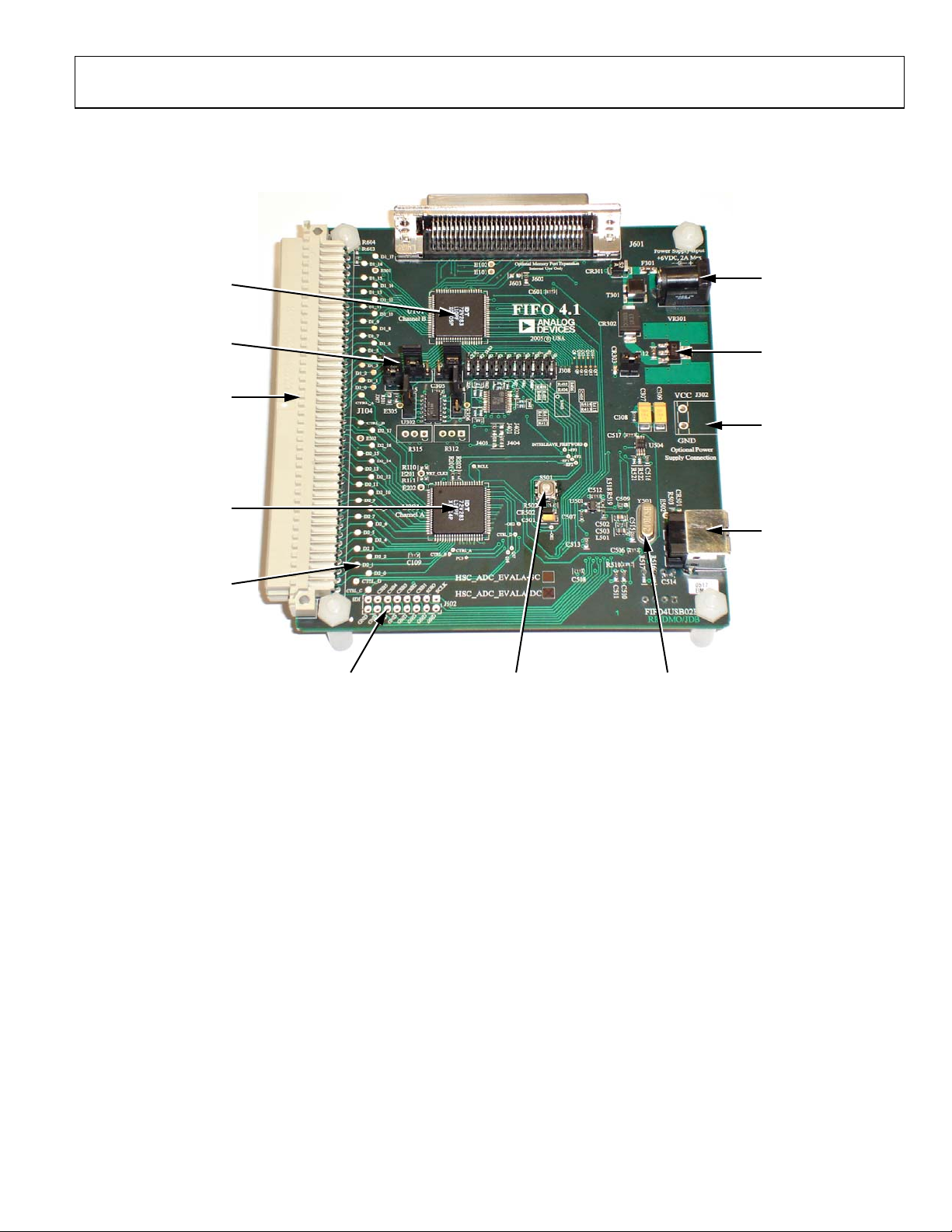
FIFO 4.1 DATA CAPTURE BOARD FEATURES
IDT72V283 32k ⋅
16-BIT 133MHz FIFO
TIMING ADJUSTMENT
16-BIT 133MHz FIFO
OPEN SOLDER MASK
CLOCK LINES FOR
JUMPERS
120-CONNECTOR
(PARALLEL CMOS
ON ALL DATA AND
INPUTS)
IDT72V283 32k ⋅
EASY PROBING
OPTIONAL SERIAL
PORT INTERFACE
CONNECTOR
RESET SWITCH
WHEN ENCODE RATE
IS INTERRUPTED
Figure 2. FIFO Components (Top View)
µCONTROLLER CRYSTAL
CLOCK = 24MHz,
OFF DURING
DATA CAPTURE
6V SWITCHING
POWER SUPPLY
CONNECTION
ON BOARD +3.3V
REGULATOR
OPTIONAL POWER
CONNECTION
USB CONNECTION
TO COMPUTER
05870-002
Rev. 0 | Page 5 of 28
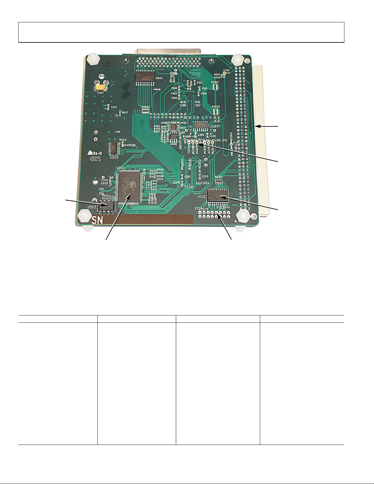
HSC-ADC-EVALB-SC/HSC-ADC-EVALB-DC
120-CONNECTOR
(PARALLEL CMOS
INPUTS)
TIMING ADJUSTMENT
JUMPERS
EPROM TO LOAD
USB FIRMWARE
DRIVER CIRCUIT FOR
SERIAL PORT INTERFACE
(SPI) LINES
CYPRESS Fx2 HIGH SPEED
USB 2.0 µCONTROLLER
Figure 3. FIFO Components (Bottom View)
OPTIONAL SERIAL
PORT INTERFACE
(SPI) CONNECTOR
05870-003
FIFO 4.1 SUPPORTED ADC EVALUATION BOARDS
The evaluation boards in Tab l e 1 can be used with the high speed ADC FIFO evaluation kit. Some evaluation boards require an adapter between
the ADC evaluation board connector and the FIFO connector. If an adapter is needed, send an email to
the part number of the adapter and a mailing address.
Table 1. HSC-ADC-EVALB-DC- and HSC-ADC-EVALB-SC-Compatible Evaluation Boards
Evaluation Board Model Description of ADC FIFO Board Version Comments
AD6644ST/PCB 14-bit, 65 MSPS ADC SC
AD6645-80/PCB
14-bit, 80 MSPS ADC SC
AD6645-105/PCB 14-bit, 105 MSPS ADC SC
AD9051/PCB 10-bit, 60 MSPS ADC SC Requires AD9051FFA
AD9200SSOP-EVAL 10-bit, 20 MSPS ADC SC Requires AD922xFFA
AD9200TQFP-EVAL 10-bit, 20 MSPS ADC SC Requires AD922xFFA
AD9201-EVAL Dual 10-bit, 20 MSPS ADC
1
SC Requires AD922xFFA
AD9203-EB 10-bit, 40 MSPS ADC SC Requires AD922xFFA
AD9212-65EB
1
Octal 10-bit, 65 MSPS ADC DC Requires HSC-ADC-FPGA-8
AD9215BCP-65EB 10-bit, 65 MSPS ADC SC
AD9215BCP-80EB 10-bit, 80 MSPS ADC SC
AD9215BCP-105EB 10-bit, 105 MSPS ADC SC
AD9215BRU-65EB 10-bit, 65 MSPS ADC SC
AD9215BRU-80EB 10-bit, 80 MSPS ADC SC
AD9215BRU-105EB 10-bit, 105 MSPS ADC SC
AD9216-80PCB Dual 10-bit, 80 MSPS ADC DC
AD9216-105PCB Dual 10-bit, 105 MSPS ADC DC
highspeed.converters@analog.com with
1
Rev. 0 | Page 6 of 28
HSC-ADC-EVALB-SC/HSC-ADC-EVALB-DC
Evaluation Board Model Description of ADC FIFO Board Version Comments
AD9218-105PCB 10-bit, 105 MSPS ADC DC
AD9218-65PCB 10-bit, 65 MSPS ADC DC
AD9219-65EB
AD9220-EB 12-bit, 10 MSPS ADC SC Requires AD922xFFA
AD9222-65EB
AD9226-EB 12-bit, 65 MSPS ADC SC Requires AD922xFFA
AD9226QFP-EB 12-bit, 65 MSPS ADC SC Requires AD922xFFA
AD9228-65EB
AD9229-65EB
AD9233-80EB 12-bit, 80MSPS ADC SC
AD9233-105EB 12-bit, 105MSPS ADC SC
AD9233-125EB 12-bit, 125MSPS ADC SC
AD9234-EB 12-bit, 150MSPS ADC SC
AD9235BCP-20EB 12-bit, 20 MSPS ADC SC
AD9235BCP-40EB 12-bit, 40 MSPS ADC SC
AD9235BCP-65EB 12-bit, 65 MSPS ADC SC
AD9235-20PCB 12-bit, 20 MSPS ADC SC
AD9235-40PCB 12-bit, 40 MSPS ADC SC
AD9235-65PCB 12-bit, 65 MSPS ADC SC
AD9236BRU-80EB 12-bit, 80 MSPS ADC SC
AD9236BCP-80EB 12-bit, 80 MSPS ADC SC
AD9237BCP-20EB 12-bit, 20 MSPS ADC SC
AD9237BCP-40EB 12-bit, 40 MSPS ADC SC
AD9237BCP-65EB 12-bit, 65 MSPS ADC
AD9238BST-20PCB Dual 12-bit, 20 MSPS ADC DC
AD9238BST-40PCB Dual 12-bit, 40 MSPS ADC DC
AD9238BST-65PCB Dual 12-bit, 65 MSPS ADC DC
AD9238BCP-20EB Dual 12-bit, 20 MSPS ADC DC
AD9238BCP-40EB Dual 12-bit, 40 MSPS ADC DC
AD9238BCP-65EB Dual 12-bit, 65 MSPS ADC DC
AD9240-EB 14-bit, 40 MSPS ADC SC Requires AD922xFFA
AD9241-EB 14-bit, 1.25 MSPS ADC SC Requires AD922xFFA
AD9243-EB 14-bit, 3 MSPS ADC SC Requires AD922xFFA
AD9244-40PCB 14-bit, 40 MSPS ADC SC
AD9244-65PCB 14-bit, 65 MSPS ADC SC
AD9245BCP-20EB 14-bit, 20 MSPS ADC
AD9245BCP-40EB 14-bit, 40 MSPS ADC
AD9245BCP-65EB 14-bit, 65 MSPS ADC
AD9245BCP-80EB 14-bit, 80 MSPS ADC
AD9246-80EB 14-bit, 80 MSPS ADC
AD9246-105EB 14-bit, 105 MSPS ADC
AD9246-125EB 14-bit, 125 MSPS ADC
AD9248BST-65EB Dual 14-bit, 65 MSPS ADC DC
AD9248BCP-20EB Dual 14-bit, 20 MSPS ADC DC
AD9248BCP-40EB Dual 14-bit, 40 MSPS ADC DC
AD9248BCP-65EB Dual 14-bit, 65 MSPS ADC DC
AD9259-50EB
AD9260-EB 16-bit, 2.5 MSPS ADC SC Requires AD922xFFA
AD9280-EB 8-bit, 32 MSPS ADC SC Requires AD922xFFA
AD9281-EB Dual 8-bit, 28 MSPS ADC SC Requires AD922xFFA
AD9283/PCB 8-bit, 100 MSPS ADC SC Requires AD9283FFA
AD9287-100EB
AD9289-65EB
AD9411/PCB 10-bit, 200 MSPS ADC DC Requires DEMUX BRD
1
1
1
1
Quad 10-bit, 65 MSPS ADC DC Requires HSC-ADC-FPGA-4/-8
Octal 12-bit, 65 MSPS ADC DC Requires HSC-ADC-FPGA-8
Quad 12-bit, 65 MSPS ADC DC Requires HSC-ADC-FPGA-4/-8
Quad 12-bit, 65 MSPS ADC DC Requires HSC-ADC-FPGA-4/-8
SC
SC
SC
SC
SC
SC
SC
SC
1
1
1
Quad 14-bit, 50 MSPS ADC DC Requires HSC-ADC-FPGA-4/-8
Quad 8-bit, 100 MSPS ADC DC Requires HSC-ADC-FPGA-4/-8
Quad 8-bit, 65 MSPS ADC DC Requires HSC-ADC-FPGA-9289
Rev. 0 | Page 7 of 28

HSC-ADC-EVALB-SC/HSC-ADC-EVALB-DC
Evaluation Board Model Description of ADC FIFO Board Version Comments
AD9430-CMOS/PCB 12-bit, 210 MSPS ADC DC
AD9430-LVDS/PCB
AD9432/PCB 12-bit, 105 MSPS ADC SC
AD9433/PCB 12-bit, 125 MSPS ADC SC
AD9444-CMOS/PCB 14 bit, 80 MSPS ADC SC
AD9444-LVDS/PCB 14 bit, 80 MSPS ADC SC
AD9445-IF-LVDS/PCB 14-bit, 125 MSPS ADC SC
AD9445-BB-LVDS/PCB 14-bit, 125 MSPS ADC SC
AD9446-80LVDS/PCB 16-bit, 80 MSPS ADC SC
AD9446-100LVDS/PCB 16-bit, 100 MSPS ADC SC
AD9460-80EB-IF 16-bit, 80 MSPS ADC SC
AD9460-80EB-BB 16-bit, 80 MSPS ADC SC
AD9460-105EB-IF 16-bit, 105 MSPS ADC SC
AD9460-105EB-BB 16-bit, 105 MSPS ADC SC
AD9461-130EB-IF 16-bit, 130 MSPS ADC SC
AD9461-130EB-BB 16-bit, 130 MSPS ADC SC
AD9480-LVDS/PCB
AD9481-PCB 8-bit, 250 MSPS ADC DC
AD10200/PCB Dual 12-bit, 105 MSPS ADC DC Requires GS09066
AD10201/PCB Dual 12-bit, 105 MSPS ADC DC Requires GS09066
AD10226/PCB Dual 12-bit, 125 MSPS ADC DC Requires GS09066
AD10265/PCB Dual 12-bit, 65 MSPS ADC DC Requires GS09066
AD10465/PCB Dual 14-bit, 65 MSPS ADC DC Requires GS09066
AD10677/PCB 16-bit, 65 MSPS ADC SC Requires GS09066
AD10678/PCB 16-bit, 80 MSPS ADC SC Requires GS09066
AD15252/PCB 12-bit, Dual 65 MSPS ADC DC
AD15452/PCB 12-bit, Quad 65 MSPS ADC DC Requires HSC-ADC-FPGA-4/-8
1
The high speed ADC FIFO evaluation kit can be used to evaluate two channels at a time.
2
If a DEMUX BRD is needed, send an email to highspeed.converters@analog.com.
2
2
12-bit, 210 MSPS ADC DC Requires DEMUX BRD
8-bit, 250 MSPS ADC DC Requires DEMUX BRD
Rev. 0 | Page 8 of 28

HSC-ADC-EVALB-SC/HSC-ADC-EVALB-DC
THEORY OF OPERATION
The FIFO evaluation board can be divided into several circuits,
each of which plays an important part in acquiring digital data
from the ADC and allows the PC to upload and process that
data. The evaluation kit is based around the IDT72V283 FIFO
chip from Integrated Device Technology, Inc (IDT). The system
can acquire digital data at speeds up to 133 MSPS and data
record lengths up to 32 kB using the HSC-ADC-EVALB-SC
FIFO evaluation kit. The HSC-ADC-EVALB-DC, which has
two FIFO chips, is available to evaluate multichannel ADCs or
demultiplexed data from ADCs sampling faster than 133 MSPS.
A USB 2.0 microcontroller communicating with ADC Analyzer
allows for easy interfacing to newer computers using the USB 2.0
(USB 1.1-compatible) interface.
The process of filling the FIFO chip or chips and reading the
data back requires several steps. First, ADC Analyzer initiates
the FIFO chip fill process. The FIFO chips are reset, using a
master reset signal (MRS). The USB microcontroller is then
suspended, which turns off the USB oscillator and ensures that
it does not add noise to the ADC input. After the FIFO chips
completely fill, the full flags from the FIFO chips send a signal
to the USB microcontroller to wake up the microcontroller
from suspend. ADC Analyzer waits for approximately 30 ms
and then begins the readback process.
During the readback process, the acquisition of data from
FIFO 1 (U201) or FIFO 2 (U101) is controlled via Signal OEA
and Signal OEB. Because the data outputs of both FIFO chips
drive the same 16-bit data bus, the USB microcontroller
controls the OEA and OEB signals to read data from the correct
FIFO chip. From an application standpoint, ADC Analyzer
sends commands to the USB microcontroller to initiate a read
from the correct FIFO chip, or from both FIFO chips in dual or
demultiplexed mode.
CLOCKING DESCRIPTION
Each channel of the buffer memory requires a clock signal to
capture data. These clock signals are normally provided by the
ADC evaluation board and are passed along with the data
through Connector J104 (Pin 37 for both Channel A and
Channel B). If only a single clock is passed for both channels,
they can be connected together by Jumper J303.
Jumpers J304 and J305 at the output of the LVDS receiver allow
the output clock to be inverted by the LVDS receiver. By default,
the clock outputs are inverted by the LVDS receiver.
The single-ended clock signal from each data channel is
buffered and converted to a differential CMOS signal by two
gates of a low voltage differential signal (LVDS) receiver, U301.
This allows the clock source for each channel to be CMOS,
TTL, or ECL.
The clock signals are ac-coupled by 0.1 μF capacitors.
Potentiometer R312 and Potentiometer R315 allow for fine
tuning the threshold of the LVDS gates. In applications where
fine-tuning the threshold is critical, these potentiometers can be
replaced with a higher resistance value to increase the
adjustment range. Resistors R301, R302, R303, R304, R311,
R313, R314, and R316 set the static input to each of the
differential gates to a dc voltage of approximately 1.5 V.
At assembly, Solder Jumper J310 to Solder Jumper J313 are set
to bypass the potentiometer. For fine adjustment using the pot,
the solder jumpers must be removed, and R312 and R315 must
be populated.
U302, an XOR gate array, is included in the design to let users
add gate delays to the FIFO memory chip clock paths. They are
not required under normal conditions and are bypassed at
assembly by Jumper J314 and Jumper J315. Jumper J306 and
Jumper J307 allow the clock signals to be inverted through an
XOR gate. In the default setting, the clocks are not inverted by
the XOR gate.
The clock paths described above determine the WRT_CLK1 and
WRT_CLK2 signals at each FIFO memory chip (U101 and
U201). The timing options above should let you choose a clock
signal that meets the setup and hold time requirements to
capture valid data.
A clock generator can be applied directly to S1 and/or S3. This
clock generator should be the same unit that provides the clock
for the ADC. These clock paths are ac-coupled, so that a sine
wave generator can be used. DC bias can be adjusted by
R301/R302 and R303/R304.
The DS90LV048A differential line receiver is used to square the
clock signal levels applied externally to the FIFO evaluation
board. The output of this clock receiver can either directly drive
the write clock of the IDT72V283 FIFO(s), or first pass through
the XOR gate timing circuitry described above.
SPI DESCRIPTION
The Cypress IC (U502) supports the HSC SPI standard to allow
programming of ADCs that have SPI-accessible register maps.
U102 is a buffer that drives the 4-wire SPI (SCLK, SDI, SDO,
1
CSB
) through the 120-pin connector (J104) on the third or top
row. J502 is an auxiliary SPI connector to monitor the SPI
signals connected directly to the Cypress IC. For more
information on this and other functions, consult the user
manual titled Interfacing to High Speed ADCs via SPI at
www.analog.com/hsc-FIFO.
1
Note that CSB1 is the default CSB line used.
Rev. 0 | Page 9 of 28
HSC-ADC-EVALB-SC/HSC-ADC-EVALB-DC
The SPI interface designed on the Cypress IC can communicate
with up to five different SPI-enabled devices. The CLK and data
lines are common to all SPI devices. The correct device is
chosen to communicate by using one of the five active low chip
select pins. This functionality is controlled by selecting a SPI
channel in the software.
CLOCKING WITH INTERLEAVED DATA
ADCs with very high data rates can exceed the capability of a
single buffer memory channel (~133 MSPS). These converters
often demultiplex the data into two channels to reduce the rate
required to capture the data. In these applications, ADC Analyzer
must interleave the data from both channels to process it as a
single channel. The user can configure the software to process
the first sample from Channel A, the second from Channel B,
and so on, or vice versa. The synchronization circuit included in
the buffer memory forces a small delay between the write enable
signals (WENA and WENB) to the FIFO memory chips (Pin 1,
U101, and U201), ensuring that the data is captured in one
FIFO before the other. Jumper J401 and Jumper J402 determine
which FIFO receives WENA and which FIFO receives WENB.
CONNECTING TO THE HSC-ADC-FPGA-4/-8
ADCs that have serial LVDS outputs require another board that
is connected between the ADC evaluation board and the FIFO
data capture card. This board converts the serial data into
parallel CMOS so that the FIFO data capture card can accept
the data. For more detailed information on this board, refer to
the HSC-ADC-FPGA datasheet at
www.analog.com/hsc-FIFO.
CONNECTING TO THE DEMUX BRD
ADCs that have parallel LVDS outputs require another board
that is connected between the ADC evaluation board and the
FIFO data capture card. This board converts parallel LVDS to
parallel CMOS, using both channels of the FIFO data capture
card. For more detailed information on this board, send an
email to highspeed.converters@analog.com
UPGRADING FIFO MEMORY
The FIFO evaluation board includes one or two 32 kB FIFOs
that are capable of 133 MHz clock signals, depending on the
model number. Pin-compatible FIFO upgrades are available
from IDT. See
Table 2. IDT Part Number Matrix
Part Number FIFO Depth FIFO Speed
IDT72V283-L7-5PF (Default ) 32 kB 133 MHz
IDT72V293-L7-5PF 64 kB 133 MHz
IDT72V2103-L7-5PF 132 kB 133 MHz
IDT72V2113-L7-5PF 256 kB 133 MHz
IDT72V283-L6PF 32 kB 166 MHz
IDT72V293-L6PF 64 kB 166 MHz
IDT72V2103-L6PF 132 kB 166 MHz
IDT72V2113-L6PF 256 kB 166 MHz
For more information, visit www.idt.com.
Table 2 for the IDT part number matrix.
Rev. 0 | Page 10 of 28

HSC-ADC-EVALB-SC/HSC-ADC-EVALB-DC
JUMPERS
Use the legends in Tab le 3 and Table 4 to configure the jumpers. On the FIFO evaluation board, Channel A is associated with the bottom
IDT FIFO chip, and Channel B is associated with the top IDT FIFO chip (closest to the Analog Devices logo).
Table 3. Jumper Legend
Position Description
In Jumper in place (2-pin header).
Out Jumper removed (2-pin header).
Position 1 or Position 3 Denotes the position of a 3-pin header. Position 1 is marked on the board.
Table 4. Solder Jumper Legend
Position Description
In Solder pads should be connected with 0 Ω resistor.
Out Solder pads should not be connected with 0 Ω resistor.
DEFAULT SETTINGS
Tabl e 5 lists the default settings for each model of the FIFO evaluation kit. The single channel (SC) model is configured to work with a
single channel ADC using the bottom FIFO, U201. The dual channel (DC) model is configured to work with demultiplexed ADCs (such
as the AD9430). Dual channel ADC settings are shown in a separate column, as are settings for the opposite (top) FIFO, U101 for a single
channel ADC. To align the timing properly, some evaluation boards require modifications to these settings. Refer to the
Description
section in the Theory of Operation section for more information.
Clocking
Another useful way to configure the jumper settings easily for various configurations is to consult ADC Analyzer under Help > About
HSC_ADC_EVALB, and click Set Up Default Jumper Wizard. Then click the configuration setting that applies to the application of
interest. A picture of the FIFO board is displayed for that application with a visual of the correct jumper settings already in place.
Table 5. Jumper Configurations
Single Channel
Settings, Default
Jumper #
J303 In Out Out In Position 2 to Position 4, ties write clocks together
J304 In In In In
J305 In In In In
J306 Out Out Out Out
J307 Out Out Out Out
J310 to
J313
J314 In In In In
J315 In In In In
J316 In In In In Power connected using switching power supply
J401 In In In In
J402 Out Out Out Out
J403 Out Out Out Out
J404 In In In In
J405 Out In Out Out
(Bottom)
In In In In
Demultiplexed
Settings
Dual-Channel
Settings
Single-Channel
Settings (Top)
1
Description
Position 1 to Position 2, POS3: invert clock out of
DS90 (U301)
Position 2 to Position 3, POS3: invert clock out of
DS90 (U301)
No invert to encode clock from XOR (U302),
0 Ω resistor
No invert to encode clock from XOR (U302),
0 Ω resistor
All solder jumpers are shorted with 0 Ω resistors
(bypass level shifting to input of DS90)
Position 1 to Position 2, one XOR gate timing
delay for top FIFO (U101)
Position 1 to Position 2, one XOR gate timing
delay for bottom FIFO (U201)
Controls if top FIFO (U101) gets write enable
before or after bottom FIFO, 0 Ω resistor
Controls if top FIFO (U101) gets write enable
before or after bottom FIFO, 0 Ω resistor
Controls if bottom FIFO (U201) gets a write
enable before or after the top FIFO, 0 Ω resistor
Controls if bottom FIFO (U201) gets a write
enable before or after the top FIFO, 0 Ω resistor
When in, WRT_CLK1 is used to create write enable
signal for FIFOs, 0 Ω resistor (significant only for
interleave mode)
Rev. 0 | Page 11 of 28

HSC-ADC-EVALB-SC/HSC-ADC-EVALB-DC
Single Channel
Demultiplexed
Settings
Jumper #
Settings, Default
(Bottom)
J406 In In In In
J503 In In In In
J504 Out Out Out Out N/A
J505 In In In In
J506 Out Out Out Out N/A
J602 Out Out Out Out N/A
J603 In In In In N/A
1
Some jumpers can be a 0 Ω resistor instead of a physical jumper. This is shown in Table 5 in the jumper description column.
Dual-Channel
Settings
Single-Channel
Settings (Top)
1
Description
WRT_CLK2 is used to create write enable signal
for FIFOs, 0 Ω resistor (significant only for
interleave mode)
Connect enable empty flag of top FIFO (U101)
to USB MCU, 0 Ω resistor
Connect enable full flag of top FIFO (U101)
to USB MCU, 0 Ω resistor
Rev. 0 | Page 12 of 28

HSC-ADC-EVALB-SC/HSC-ADC-EVALB-DC
T
EVALUATION BOARD
The FIFO provides all of the support circuitry required to
accept two channels of an ADC’s digital parallel CMOS outputs.
Each of the various functions and configurations can be selected by
proper connection of various jumpers (see
Tabl e 5). When
using this in conjunction with an ADC evaluation board, it is
critical that the signal sources used for the analog input and
clock have very low phase noise (<1 ps rms jitter) to realize the
ultimate performance of the converter. Proper filtering of the
analog input signal to remove harmonics and lower the integrated
or broadband noise at the input is also necessary to achieve the
specified noise performance.
Figure 5 to Figure 15 for complete schematics and layout plots.
See
POWER SUPPLIES
The FIFO board is supplied with a wall mount switching power
supply that provides a 6 V, 2 A maximum output. Connect the
supply to the rated 100 ac to 240 ac wall outlet at 47 Hz to 63 Hz.
The other end is a 2.1 mm inner diameter jack that connects to
the PCB at J301. On the PC board, the 6 V supply is then fused
and conditioned before connecting to the low dropout 3.3 V
linear regulator that supplies the proper bias to the entire board.
WALL OUTLE
100V TO 240V AC
47Hz TO 63Hz
SWITCHING
POWER
SUPPLY
EVALUATION
XFMR
INPUT
CLK
BOARD
ROHDE & SCHWARZ,
SMHU,
2V p-p SIGNAL
SYNTHESIZER
ROHDE & SCHWARZ,
SMHU,
2V p-p SI GNAL
SYNTHESIZER
BAND-PASS
FILTER
Figure 4. Example Setup Using Quad ADC Evaluation Board and FIFO Data Capture Board
PAR ALL EL
OUTPUTS
PAR ALL EL
OUTPUTS
When operating the evaluation board in a non-default
condition, J316 can be removed to disconnect the switching
power supply. This enables the user to bias the board
independently. Use P302 to connect an independent supply to
the board. A 3.3 V supply is needed with at least a 1 A current
capability.
CONNECTION AND SETUP
The FIFO board has a 120-pin (40-pin, triple row) connector
that accepts two 16-bit channels of parallel CMOS inputs (see
Figure 6). For those ADC evaluation boards that have only an
80-pin (40-pin, double row) connector, it is pertinent for the
lower two rows of the FIFO’s triple row connector to be connected
in order for the data to pass to either FIFO channel correctly.
The top or third row is used to pass SPI signals across to the
adjacent ADC evaluation board that supports this feature.
3.3V
–+
VCC
GND
HSC-ADC-EVALB-DC
FIFO DATA
CAPTURE
BOARD
USB
CONNECT ION
SPI
PC
RUNNING
ADC
ANALYZER
SPISPI
05870-004
CHB
CMOS
CHB
CMOS
6V DC
2A MAX
Rev. 0 | Page 13 of 28

HSC-ADC-EVALB-SC/HSC-ADC-EVALB-DC
A
FIFO SCHEMATICS AND PCB LAYOUT
SCHEMATICS
LLOW Fx2 TO CONTROL FIFO’S OUTPUT WIDTH
PC2: TRISTATED, NORMAL 16-BIT DATA PATH
PC2: DRIVEN HIG H, 9-BIT OUTPUT ALLOWS
READING 18 BITS IN TWO READS.
10kΩ
EF1_TF
REN1
RCLK
E101
VCC
PC2
R1010ΩR102
WRT_CLK1
MRS
FF1_TF
WRT_CLK1
R108
DNP
R109
DNP
VCC
75
76
80
WEN1
E102
POPULATE WITH PIN SOCKET
D1_17
D1_16
D1_15
D1_14
D1_13
D1_12
D1_11
D1_10
D1_9
D1_8
1
2
3
4
5
6
7
8
9
10
11
12
13
14
15
16
17
18
19
20
U101
WEN
SEN
DNC
VCC
DNC
IW
GND
D17
VCC
D16
D15
D14
D13
GND
D12
D11
D10
D9
D8
VCC
WCLK
D7
21
77
78
79
LD
PRS
MRS
D6
GND
23
24
22
FF/IR
FWFT/SI
D5
D4D3D2D1D0
26
25
72
73
74
OW
PAF
70
71
HF
FSEL1
FSEL0
IDT72V283
TQFP80
TOP FIFO
CHANNEL B
Q0
GND
31
30
29
28
27
67
68
69
IP
BE
VCC
Q1
Q2
GND
32
33
34
64
65
66
PAE
PFM
Q3
VCC
36
35
62
63
61
RM
REN
RCLK
EF/OR
Q4
Q5
GND
39
37
38
60
RT
59
OE
VCC
Q17
Q16
GND
GND
Q15
Q14
VCC
Q13
Q12
GND
Q11
GND
Q10
VCC
Q9
Q8
Q7
Q6
40
OE1
58
57
Q17
56
Q16
55
54
53
Q15
52
Q14
51
50
Q13
49
Q12
48
47
Q11
46
45
Q10
44
43
Q9
42
Q8
41
Q7
D1_1
D1_0
D1_2
C106
0.1µF
Q0
C107
0.1µF
Q1
C108
0.1µF
Q2
Q3
C109
0.1µF
Q4
Q5
Q6
5870-005
VCC
C101
0.1µF
C102
0.1µF
D1_3
D1_5
C104
0.1µF
D1_4
C105
0.1µF
D1_7
D1_6
C103
0.1µF
Figure 5. PCB Schematic
Rev. 0 | Page 14 of 28

HSC-ADC-EVALB-SC/HSC-ADC-EVALB-DC
CMOS INPUTS
CHB
CHA
J104
CLKB
MSB
LSB
CLKA
MSB
LSB
A1
A2
A3
A4
A5
A6
A7
A8
A9
A10
A11
A12
A13
A14
A15
A16
A17
A18
A19
A20
A21
A22
A23
A24
A25
A26
A27
A28
A29
A30
A31
A32
A33
A34
A35
A36
A37
A38
A39
A40
TEST POINTS
D1_15
D1_14
D1_13
D1_12
D1_11
D1_10
D1_9
D1_8
D1_7
D1_6
D1_5
D1_4
D1_3
D1_2
D1_1
D1_0
CTRL_B
D2_15
D2_14
D2_13
D2_12
D2_11
D2_10
D2_9
D2_8
D2_7
D2_6
D2_5
D2_4
D2_3
D2_2
D2_1
D2_0
CTRL_D
DUT_CLK1
D1_15
D1_14
D1_13
D1_12
D1_11
D1_10
D1_9
D1_8
D1_7
D1_6
D1_5
D1_4
D1_3
D1_2
D1_1
D1_0
CTRL_B
DUT_CLK2
D2_15
D2_14
D2_13
D2_12
D2_11
D2_10
D2_9
D2_8
D2_7
D2_6
D2_5
D2_4
D2_3
D2_2
D2_1
D2_0
CTRL_D
J104
B1
B2
B3
B4
B5
B6
B7
B8
B9
B10
B11
B12
B13
B14
B15
B16
B17
B18
B19
B20
B21
B22
B23
B24
B25
B26
B27
B28
B29
B30
B31
B32
B33
B34
B35
B36
B37
B38
B39
B40
TEST POINTS
D1_17
D1_16
CTRL_A
D2_17
D2_16
CTRL_C
D1_17
D1_16
CTRL_A
D2_17
D2_16
CTRL_C
PLACEMENT OF HEADER KEY HERE
J104
C1
C2
C3
C4
C5
C6
C7
C8
C9
C10
C11
C12
C13
C14
C15
C16
C17
C18
C19
C20
C21
C22
C23
C24
C25
C26
C27
C28
C29
C30
C31
C32
C33
C34
C35
C36
C37
C38
C39
C40
SDO
ALL SPI LABELS ARE WITH
RESPECT TO THE DUT.
19
18
16
15
14
13
12
11
10
1
2
17
3
16
15
4
14
5
6
13
7
22
9
RZ101
12
11
8
20
OE2
Y0
Y1
U102
Y2
74VHC541MTC
Y3
Y4
Y5
Y6
Y7
GND
10
VCC
VCC
1
OE
2
A0
3
A1
A2
A3
A4
A5
A6
A7
CSB1
4
CSB2
5
6
SCLK
7
CSB3
8
CSB4
9
R103
10kΩ
R104
10kΩ
SDI
PLACEMENT OF HEADER KEY HERE
Figure 6. Schematic (Continued)
Rev. 0 | Page 15 of 28
05870-006
HSC-ADC-EVALB-SC/HSC-ADC-EVALB-DC
A
E201
VCC
TE WITH PI N SOCKET
POPUL
E202
WEN2
D2_17
D2_16
D2_15
D2_14
D2_13
D2_12
D2_11
D2_10
D2_9
D2_8
WRT_CLK2
1
WEN
2
SEN
3
DNC
4
VCC
5
DNC
6
IW
7
GND
8
D17
9
VCC
10
D16
11
D15
12
D14
13
D13
14
GND
15
D12
16
D11
17
D10
18
D9
19
D8
20
VCC
U201
MRS
76
80
WCLK
D7
21
77
78
79
LD
PRS
MRS
D5
D6
GND
23
25
24
22
PC3
R2010ΩR202
FF2
75
FF/IR
FWFT/SI
72
73
74
OW
PAF
BOTTOM FIFO
D4D3D2D1D0
29
28
27
26
10kΩ
70
71
HF
FSEL1
FSEL0
IDT72V283
TQFP80
CHANNEL A
Q0
GND
31
30
EF2
67
68
69
IP
BE
VCC
Q1
Q2
GND
32
33
34
64
65
66
PAE
PFM
EF/OR
Q3
Q4
VCC
36
35
37
REN2
RCLK
62
63
61
RM
REN
RCLK
Q5
GND
39
38
60
RT
59
OE
VCC
Q17
Q16
GND
GND
Q15
Q14
VCC
Q13
Q12
GND
Q11
GND
Q10
VCC
Q9
Q8
Q7
Q6
40
OE2
58
57
Q17
56
Q16
55
54
53
Q15
52
Q14
51
50
Q13
49
Q12
48
47
Q11
46
45
Q10
44
43
Q9
42
Q8
41
Q7
R203
DNP
R204
DNP
VCC
WRT_CLK2
VCC
C201
0.1µF
C202
0.1µF
Q0
Q1
Q2
Q3
Q4
Q5
D2_1
D2_3
D2_5
D2_7
D2_6
C203
0.1µF
D2_4
C204
0.1µF
C205
0.1µF
D2_0
D2_2
C206
C207
0.1µF
C208
0.1µF
0.1µF
Q6
05870-007
Figure 7. Schematic (Continued)
Rev. 0 | Page 16 of 28

HSC-ADC-EVALB-SC/HSC-ADC-EVALB-DC
R
R
TOP FIFO
WRT_CLK1
CONTROLS
3
J314
6
U302
4
U302
1
C305
R303
0.1µF
BOTTOM FIFO
C303
13
6
9
DUT_CLK2
0.1µF
331Ω
R302
331Ω
INVERT CLOCK 1
VCC
EN
EN
R304
VCC
TOP FIFO
DUT_CLK1
C302
0.1µF
E301E302
PIN SOCKET
POPULATE WITH
VCC
VCC
R301
331Ω
GATE DELAYS
1
SET 0, 1, OR 2 XO
E306
74VCX86
5
3
74VCX86
1kΩ
R309
2
J306
3
J304
1
14
15
ROUT2
ROUT1
DS90LV048A
RIN1+
RIN1–1RIN2+3RIN2–4RIN3+6RIN3–5RIN4+7RIN4–
2
J303
331Ω
INVERT CLOCK 1
VCC
VCC
2
1
DNP
R310
1kΩ
J307
C306
0.1µF
INVERT CLOCK 2
ROUT311ROUT4
4
3
R314
331Ω
DNP
J312
12
12U301
J313
DNP
CHANNEL CONFIG URATION
74VCX86
INVERT CLOCK 2
ON TOP SIDE
GATE DELAYS
1
SET 0, 1, O R 2 XO
WRT_CLK2WRT_CLK1
RCLK
E305
2
74VCX86
C311
0.1µF
R316
331Ω
J308
1
34
56
VCC
AUX CLOCK SIGNAL MONITOR CONNECTOR
VR301
ADP3339AKC-3.3
CR302
SK33MSCT
T103
12
PLACE JUMPERS BETWEEN PADS
F301
EF2
FF2
10
11 12
78
9
FF1_F
EF1_F
TOP FIFO BOTTOM FIFO
2
VOVI
4
VO
3
43
CR301
S2A
2.2A
C301
10µF
+
OE2
13 14
OE1
C313
ADJ
C312
REN2
15 16
REN1
J316
12
1µF
1
1µF
WENS
20
DNP
17 18
19
MRS
OPTIONAL POWER
R317
C309
+
C308
C307
+
INPUT HEADER
CR303
499Ω
10µF
0.1µF
10µF
J302
VCC
12
DNP
CONTROL S
WRT_CLK2
BOTTOM FIFO
3
J315
11
U302
13
8
U302
9
10
1
J305
3
10
GND
8
REMOVE JUMPER FOR DUAL
R315
C310
0.1µF
SHORT C302 AND C303
REMOVE R301- R304 AND
FOR COHERENT SAMPL ING
J310
VCC
R311
331Ω
R312
J311
DNP
R313
331Ω
Figure 8. Schematic (Continued)
POWER SUPPLY INPUT 6V, 2A MAX
J301
PJ-102A
132
5870-008
Rev. 0 | Page 17 of 28

HSC-ADC-EVALB-SC/HSC-ADC-EVALB-DC
CONTROLS TOP FI FO
CONTROLS BOTTOM FIFO
WEN2
WEN1
DNP
J403
J404
J401
J402
DNP
6
U403
MC100EPT23
4
3
R414
49.9Ω
R415
40.2Ω
R413
49.9Ω
R412
R411
7
U403
MC100EPT23
1
2
40.2Ω
49.9Ω
R410
49.9Ω
S0 18
R0 19
Q0 17
Q0 16
S
R
3
VBB
Q
Q
D
CLK
MC100EP29
VCC
VCC
10
R406
40.2Ω
R405
49.9Ω
1
R404
49.9Ω
7
VCC
DNP
R402
R401
20KΩ
WENS
1D0
2
R403
DNP
C401
2D0
U401
DNP
4CLK0
5CLK0
6CLK
MC100EPT22
S1 13
S
8D1
6
DNP
R1 12
Q
Q
CLK
GND
11
U402
9D1
R409
R408
R407
4
J406
40.2Ω
49.9Ω
49.9Ω
WRT_CLK2
Q1 15
Q1 14
R
D
7CLK
3
U401
MC100EPT22
J405
WRT_CLK1
C405
0.1µF
C404
0.1µF
C403
0.1µF
C402
0.1µF
VCC
05870-009
Figure 9. Schematic (Continued)
Rev. 0 | Page 18 of 28

HSC-ADC-EVALB-SC/HSC-ADC-EVALB-DC
123456789101112131415
DNP
J502
CONTROL FIFO
Q16
72
DPLUS
18
Q17
PC0/GPIFADR0
PC2
PC1/GPIFADR1
DMINUS
PC3
757473
PC2/GPIFADR2
U502
A0
OUTPUT W IDTH
PC3/GPIFADR3
CY7C68013_128AXC
A1
76
PC4/GPIFADR4
A2
77
PC5/GPIFADR5
A3
9796959419
PC6/GPIFADR6
VCC;17,26, 43,48,64, 68,81,100,107
GND;20;27; 49;58;65;80; 93;116 ;12 5
A4
117
PC7/GPIFADR7
A5
118
SDI
CSB1
CSB2
SCLK
111
110
1087978
109
PE2/T2OUT
PE0/T0OUT
PE1/T1OUT
SDO
CSB5
CSB3
CSB4
15
115
114
113
112
PE5/INT6
PE6/T2EX
PE4/RXD1OUT
PE3/RXD0OUT
PE7/GPI FADR8
16
14
NC3
NC2
NC1
ALL SPI
TO THE DUT
LABELSARE
WITH RESPECT
A15
A14
A13
A12
A11
A10A9A8
A7
A6
119
120
21
128
127
126
25
242322
INTERLEAVE _ F I R S T W O R D
OE1
CTRL_A
CTRL_B
CTRL_C
R504 24.9Ω
R505 24.9Ω
R506 24.9Ω
82
28
106
OE2
CTRL_D
R507 24.9Ω
R520 24.9Ω
R525 24.9Ω
R526 24.9Ω
929190
89
858483
INT4
PA1/I NT1
PA0/I NT0
Q0
Q1
Q2
Q3
Q4
Q5
Q6
Q7
Q8
Q9
Q10
Q11
C501
1µF
S501 = RESET USB CONTROLLER
+
3
4
Q12
Q13
Q14
Q15
S501
1
2
FF_USB
VCC
R502
100kΩ
CR502
VCC
C503
PB1/FD1
45
PB2/FD2
46
PB3/FD3
47
PB4/FD4
54
PB5/FD5
55
PB6/FD6
56
PB7/FD7
57
PD0/FD8
102
PD1/FD9
103
104
105
121
122
123
124
RXD1
53
TXD1
52
RXD0
51
TXD0
50
101
RESET
99
DVCC
2
AVCC
10
IFCLK
CLKOUT INT5
1
32
0.1µF
PB0/FD0
44
PA3/ *WU2
PA2/ *SLOE
PA6/ *PKTEND
PA5/FIFOADR1
PA4/FIFOADR0
PA7/*F LAG/SLC S
PD2/FD10
PD3/FD 11
PD4/FD12
PD5/FD13
PD6/FD14
PD7/FD15
*WAKEU P
RDY1/*SLWR
RDY0/*SLR D
4
RDY5
RDY4
RDY3
RDY2
XTALIN
XTALOUT
98765
11
12
D7
D6
D5
D4
D3
D2
D1
D0
T0
T1
T2
CTL5
CTL4
CTL3
CTL2/*FLAGC
CTL1/*FLAGB
CTL0*FLAG A
RESE RVED
BKPT
EA
SCL
SDA
OE
PSEN
RD
WR
CS
GND
AGND
16
CONNECTIO N
AUX SPI PORT
88
87
86
63
62
61
60
59
29
30
31
98
67
66
71
70
69
33
34
35
36
37
38
39
40
41
42
3
13
REN2M
R515 24.9Ω
REN2
R514 24.9Ω
R513 24.9Ω
R512 24.9Ω
R511 24.9Ω
R510 24.9Ω
R509 10kΩ
R508 10kΩ
VCC
RENEXT
REN1
WENS
MRS
2kΩ
2kΩ
R516
R517
VCC
5
6
7
8
WP
SCL
SDA
VCC
A0
A1
VSS
A2
U503
1
2
4
3
RCLK
C502
2.2µF
L501
12
VCC
FF_USB
4
3
5
+V
GND
VCC
1
2
U501
R518
10kΩ
R519
10kΩ
FF2
FROM TO P FIFO
FIFO
FROM
BOT TOM
J503
J504
DNP
J506 J505
EF1_BHB EF1_TF
FF1_BHB FF1_TF
FF2
EF2
1423
Y501
24MHz
1
2
12pF
C504
12pF
C505
J501
R503
E502
USB_VBUS
499Ω
CR501
C517
0.1µF
C516
0.1µF
C515
0.1µF
INTERLEAVE_FIRSTWORD
0Ω
C514
0.1µF
DNP
USB CONNECTIO N
E503
E504
E505
GROUND TEST POINTS
C513
0.1µF
C512
0.1µF
C511
0.1µF
C510
0.1µF
VCC
VCC
R522
C509
0.1µF
C508
0.1µF
C507
0.1µF
C506
0.1µF
VCC
R524
R523
2kΩ
VCC
6
U505
5
MRS
6
5
3
Q
Q
8
VCC
U504
7
4
332Ω
U505
3
FF1_TF
4
GND
CLK
D
PRE CLR
2
1
VCC
2
R521
332Ω
7
14
U505
VCC
1
TOP
FIFO
FROM
FIFO
FROM
FF2
BOT TOM
05870-010
Figure 10. Schematic (Continued)
Rev. 0 | Page 19 of 28

HSC-ADC-EVALB-SC/HSC-ADC-EVALB-DC
V
D1_8
D1_9
D1_10
D1_12
D1_13
D1_14
D1_15
D1_0
D1_1
D1_2
D1_3 DC3
D1_4
D1_5
D1_6
D1_7
1
2
3
4
5
6
7
RZ601
1
2
3
4
5
6
7
89
RZ602
R603
0Ω
R604
0Ω
EXTERNAL MEMORY OVERRIDES ON BOARD MEMORIES WHEN PLUGGED IN. ONLY A SIDE DATA.
16
DC8
15
DC9
14
DC10
13
DC11D1_11
12
DC12
11
DC13
10
DC14
98
DC15
16
DC0
15
DC1
14
DC2
13
12
DC4
11
DC5
10
DC6
DC7
DC16D1_16
DC17D1_17
CONNECTIONS FOR 2M WO RD EXTERNAL MEMORY
DNP
J601
35
1
DC0
DC3
DC2
DC6
DC8
DC7
DC11
DC10
DC13
DC4
DC5
DC9
DC17
EF1_BHB
FF1_BHB
WRT_CLK1
QL0
QL3
QL4
QL7
36
2
37
3
4
38
5
39
6
40
7
41
8
42
9
43
44
10
45
11
46
12
47
13
48
14
49
15
50
16
51
17
52
18
53
19
54
20
55
21
56
22
57
23
58
24
59
25
60
26
61
27
62
28
63
29
64
30
65
31
66
32
67
33
68
34
DC14
DC15
DC16
DC1
DC12
REN1
RCLK
MRS
WEN1
QL1
QL2
QL5
QL6
RENEXT
QL0
QL1
QL2
QL3
QL4
QL5
QL6
QL7
1
2
3
4
5
6
7
8
9
10
J603: ALLOW S 2 MEG BUF FER TO READ BACK DATA
ON EACH RCLK EDGE.
J602: ALLOW S 2 MEG BUF FER TO READ BACK 1 DATA
ON EVERY 3RD RCLK EDGE. J602 IS FOR
BACKWARD COMPATABILITY IF NEEDED.
Figure 11. Schematic (Continued)
CC
C601
0.1µF
U601
D0
D1
D2
D3
D4
D5
D6
D7
GND
74LCX574
REN2M RCLK
VCCOUT_EN
Q0
Q1
Q2
Q3
Q4
Q5
Q6
Q7
CLOCK
J602
DNP
20
VCC
19
18
17
16
15
14
13
12
11
1
2
3
4
5
6
7
J603
16
15
14
13
12
11
10
98
RZ605
Q0
Q1
Q2
Q3
Q4
Q5
Q6
Q7
05870-011
Rev. 0 | Page 20 of 28
HSC-ADC-EVALB-SC/HSC-ADC-EVALB-DC
PCB LAYOUT
05870-012
Figure 12. Layer 1—Primary Side
Figure 13. Layer 2—Ground Plane
Rev. 0 | Page 21 of 28
05870-013
HSC-ADC-EVALB-SC/HSC-ADC-EVALB-DC
05870-014
Figure 14. Layer 3—Power Plane
05870-015
Figure 15. Layer 4—Secondary Side
Rev. 0 | Page 22 of 28

HSC-ADC-EVALB-SC/HSC-ADC-EVALB-DC
BILL OF MATERIALS
Table 6. HSC-ADC-EVALB-SC/HSC-ADC-EVALB-DC Bill of Materials
Item Qty Reference Designation Device Package Description Manufacturer Mfg Part Number
1 42 C101 to C109, C201 to C208,
C302, C303, C305, C306, C308,
C310, C311, C402 to C405,
C503, C506 to C517, C601
2 3 C301, C307, C309 Capacitor 6032-28 Tantalum, 10 μF, 16 V,
3 2 C312, C313 Capacitor 603 Ceramic, 1 μF, 10 V,
4 1 C501 Capacitor 3216-18 Tantalum, 1 μF, 16 V,
5 1 C502 Capacitor 805 Ceramic, 2.2 μF, 25 V,
6 2 C504, C505 Capacitor 402 Ceramic, 12 pF,
7 1 CR301 Diode DO-214AA Schottky diode,
8 1 CR302 Diode DO-214AB Schottky diode,
9 2 CR303, CR501 LED 603 Green, 4 V 5 m,
10 1 CR502 Diode SOD-123 Switching, 75 V,
11 1 F301 Fuse 1210 6.0 V, 2.2 A trip current
12 1 J104 Connector 120-pin, female,
13 1 J301 Connector 0.08”, PCMT RAPC722, power
14 1 J303 Connector 4-pin Male, straight,
15 4 J304, J305, J314, J315 Connector 3-pin Male, straight, 100 mil SAMTEC TWS-103-08-G-S
16 8 J310 to J313, J401, J404, J406,
J603
17 1 J316 Connector 2-pin Male, straight, 100 mil SAMTEC TSW-1002-08-G-S
18 1 J501 Connector 4-pin USB, PC mount, right
19 1 L501 Ferrite
20 5 R101, R201, R524, R603, R604 Resistor 402 0 Ω, 1/16 W, 5% Panasonic ERJ-2GE0R00X
21 8 R102 to R04, R202, R508, R509,
R518, R4519
22 10 R301 to R304, R311, R313,
R314, R316, R521, R522
23 2 R309, R310 Resistor 402 1 kΩ, 1/16 W, 1% Panasonic ERJ-2RKF1002X
24 2 R317, R503 Resistor 402 499 Ω, 1/16 W, 1% Panasonic ERJ-2RKF1001X
25 1 R401 Resistor 402 20 kΩ, 1/16 W, 1% Panasonic ERJ-2RKF4990X
26 8 R404, R405, R407, R408, R410,
R411, R413, R414
27 4 R406, R409, R412, R415 Resistor 402 40.2 Ω, 1/16 W, 1% Panasonic ERJ-2RKF40R2X
28 1 R502 Resistor 402 100 kΩ, 1/16 W, 1% Panasonic ERJ-2RKF1003X
29 13 R504, R506, R507, R510 to R515,
R520, R525, R526
30 3 R516, R517, R523 Resistor 402 2 kΩ, 1/16 W, 1% Panasonic ERJ-2RKF2001X
31 1 RZ101 Resistor Resistor array, 22 Ω,
32 1 S501 Switch Momentary (normally
Capacitor 402 Ceramic, 0.1 μF, 16 V,
Connector 603 2-pin solder jumper,
805 500 mA, 600 Ω @
Bead
Resistor 402 10 kΩ, 1/16 W, 1% Panasonic ERJ-2RKF1002X
Resistor 402 332 Ω, 1/16 W, 1% Panasonic ERJ-2RKF3320X
Resistor 402 49.9 Ω, 1/16 W, 1% Panasonic ERJ-2RKF2002X
Resistor 402 24.9 Ω, 1/16 W, 1% Panasonic ERJ-2RKF24R9X
Rev. 0 | Page 23 of 28
X5R, 10%
10%
X5R, 10%
20%
X5R 10%
NPO, 50 V, 5%
50 V, 2 A, SMC
30 V, 3 A, SMC
candela
150 mA
resettable fuse
PC mount, right angle
supply connector
100 mil
0 Ω, 1/10 W, 5%
angle, Type B, female
100 MHz
1/4 W, 5%
open), 100 GE, 5 mm,
SPST
Panasonic ECJ-0EB1C014K
Kemet T491C106K016AS
Panasonic ECJ-1VB1A105K
Panasonic ECS-T1CY105R
Panasonic ECJ-2FB1E225K
Panasonic ECJ-0EC1H120J
Micro Commercial
Group
Micro Commercial
Group
Panasonic LNJ314G8TRA
Diodes, Inc. 1N4148W-7
Tyco, Raychem NANOSMDC110F-2
AMP 650874
Switchcraft SC1153
SAMTEC TSW-1-10-08-GD
Panasonic ERJ-3GEY0R00V
AMP 787780-1
Steward HZ0805E601R-00
Panasonic EXB-2HV220JX
Panasonic EVQ-PLDA15
S2A
SK33MSCT

HSC-ADC-EVALB-SC/HSC-ADC-EVALB-DC
Item Qty Reference Designation Device Package Description Manufacturer Mfg Part Number
33 1 T301 Choke 2020 10 μH, 5 A, 50 V,
3412 U101, U201 IC TQFP80 3.3 V,
35 1 U102 IC SOIC20 74VHC541,
36 1 U301 IC SOIC16 DS90LV048A National
37 1 U302 IC SOIC14 74VCX86 Fairchild 74VCX86
38 1 U401 IC SO8M1 MC100EPT22D Motorola MC100EPT22D
39 1 U402 IC TSSOP20 MC100EP29DT ON Semiconductor MC100EP29DT
40 1 U403 IC SO8M1 MC100EPT23D Motorola MC100EPT23D
41 1 U501 IC SOT23L5 NC7SZ32M5,
42 1 U502 IC TQFP128 CY7C68013 Cypress CY7C68013-128AXC
43 1 U503 IC DIP8 24LC00P Microchip 24LC00P
44 1 U504 IC DCT_8PIN_06,
5 mm
45 1 U505 IC SOIC 14 74LVQ04SC, low
46 1 U601 IC DIP20/SOL 74LCX574WM-ND,
47 1 VR301 IC SOT-223HS High accuracy,
48 1 Y501 Crystal Crystal Oscillator, 24 MHz Ecliptek EC-12-24.000M
49 6 See schematic for placement Connector 100 mil
50 4 Insert from bottom side of
51 2 See schematic for placement Connector Third-row
1
Only U201 is populated for the single-channel version (HSC-ADC-EVALB-SC).
board
Standoff Plastic mount
jumper
standoffs
header key
190 Ω @ 100 MHz
IDT72V283L7-5PF
octal buffer/line
driver, three-state
NC7SZ32, tiny log
UHS 2-input or gate
SN74LVC2G74DCTR,
D-type flip-flop,
DCT_8PIN_0.65MM
voltage hex inverter
74LCX574 octal D-type
flip-flop
ADP3339AKC-3.3, 3.3 V
0.1” jumpers Samtec SNT-100-BK-G-H
7/8” height, standoffs Richco CBSB-14-01A-RT
These header inserts
for J104, Pin 81, and
Pin 120 are located
on the edges of the
top row
Murata DLW5BSN191SQ2L
IDT IDT72V283L7-5PF
Fairchild 74VHC541M
DS90LV048A
Semiconductor
Fairchild NC7SZ32M5
or
CY7C68014A-128AXC
Texas Instruments SN74LVC2G74DCTR
Fairchild 74LVQ04SC
Fairchild 74LCX574WM-ND
Analog Devices ADP3339AKC-3.3
Samtec TSW-104-07-T-S
Rev. 0 | Page 24 of 28

HSC-ADC-EVALB-SC/HSC-ADC-EVALB-DC
ORDERING INFORMATION
ORDERING GUIDE
Model Description
HSC-ADC-EVALB-SC Single FIFO Version of USB Evaluation Kit
HSC-ADC-EVALB-DC Dual FIFO Version of USB Evaluation Kit
HSC-ADC-FPGA-4/-8
HSC-ADC-FPGA-9289 Quad Serial LVDS to Dual Parallel CMOS Interface for the AD9289 Only (Not Included in Evaluation Kit)
AD922XFFA
AD9283FFA
AD9059FFA
AD9051FFA
LG-0204A
1
If an adapter is needed, send an email to highspeed.converters@analog.com.
1
1
1
1
1
ESD CAUTION
ESD (electrostatic discharge) sensitive device. Electrostatic charges as high as 4000 V readily accumulate on
the human body and test equipment and can discharge without detection. Although this product features
proprietary ESD protection circuitry, permanent damage may occur on devices subjected to high energy
electrostatic discharges. Therefore, proper ESD precautions are recommended to avoid performance
degradation or loss of functionality.
Quad/Octal Serial LVDS to Dual Parallel CMOS Interface; supports all Quad/Octal ADCs in this family except
the AD9289 (not Included in Evaluation Kit)
Adapter for AD922x Family (Not Included in Evaluation Kit)
Adapter for the AD9283 and AD9057 (Not Included in Evaluation Kit)
Adapter for the AD9059 (Not Included in Evaluation Kit)
Adapter for the AD9051 (Not Included in Evaluation Kit)
Adapter for the AD10xxx and AD13xxx Families (Not Included in Evaluation Kit)
Rev. 0 | Page 25 of 28

HSC-ADC-EVALB-SC/HSC-ADC-EVALB-DC
NOTES
Rev. 0 | Page 26 of 28

HSC-ADC-EVALB-SC/HSC-ADC-EVALB-DC
NOTES
Rev. 0 | Page 27 of 28

HSC-ADC-EVALB-SC/HSC-ADC-EVALB-DC
NOTES
©2006 Analog Devices, Inc. All rights reserved. Trademarks and
registered trademarks are the property of their respective owners.
EB05870-0-2/06(0)
Rev. 0 | Page 28 of 28
 Loading...