

Page 1

Evaluation Kit for the
PRODUCT DESCRIPTION
This evaluation board allows the ADM1191/ADM1192 devices
to be easily evaluated. The ADM1191/ADM1192 are integrated
current sense amplifiers that offer digital current and voltage
monitoring via an on-chip analog-to-digital converter (ADC)
communicated through an I
sense amplifier senses voltage across the sense resistor in the
power path via the VCC and SENSE pins.
The ADC can measure the current seen in the sense resistor
and the supply voltage on the VCC pin. An industry standard
2
I
C interface allows a controller to read current and voltage data
from the ADC. Measurements can be initiated by an I
command. Alternatively, the ADC can run continuously, and
the latest conversion can be read whenever it is required.
The devices have a SETV pin. A voltage applied to this pin is
internally compared to the output voltage on the current sense
amplifier. The output of the SETV comparator asserts when the
current sense amplifier output exceeds the SETV voltage.
When this event occurs for the ADM1191, the ALERTB output
asserts; when the event occurs for the ADM1192, the ALERT
output asserts. This alert signal can be used as a flag to warn a
microcontroller or field programmable gate array (FPGA) of an
overcurrent condition. The alert output of multiple devices can
be tied together and used as a combined alert.
2
C interface. An internal current
2
C
C6
ADM1191/ADM1192
EVAL-ADM1191/ADM1192
EVALUATION BOARD DESCRIPTION
The ADM1191/ADM1192 digital power monitor evaluation
board can be controlled using the configuration tool, allowing
the device to be actively simulated through software. This
evaluation board provides an I
power supply of between 3.15 V and 26 V connected through
the J2 and J4 connectors. The latest version of the configuration
tool can be downloaded from the Analog Devices, Inc., website
www.analog.com/powermonitorsw.
Note that, when changing devices, the software should first be
shut down and the power supply to the board removed. J7 is an
2
I
C connector that connects the evaluation board to a PC via a
5-pin SMBus cable.
PACKAGE CONTENTS
ADM1191/ADM1192 evaluation board
5-pin SMBus cable
5-pin interconnection cable
ADM1191/ADM1192 device samples
R8
PIN 1 IDENTIFIER
2
C interface requiring a bench
ADM1191/ADM1192 DEVICESOCKET
Figure 1. Sample Device Placement
Rev. 0
Evaluation boards are only intended for device evaluation and not for production purposes.
Evaluation boards are supplied “as is” and without warranties of any kind, express, implied, or
statutory including, but not limited to, any implied warranty of merchantability or fitness for a
particular purpose. No license is granted by implication or otherwise under any patents or other
intellectual property by application or use of evaluation boards. Information furnished by Analog
Devices is believed to be accurate and reliable. However, no responsibility is assumed by Analog
Devices for its use, nor for any infringements of pate nts or other rights of third parties t hat may result
from its use. Analog Devices reserves the right to change devices or specifications at any time
without notice. Trademarks and registered trademarks are the property of their respective owners.
Evaluation boards are not authorized to be used in life support devices or systems.
6486-001
One Technology Way, P.O. Box 9106, Norwood, MA 02062-9106, U.S.A.
Tel: 781.329.4700 www.analog.com
Fax: 781.461.3113 ©2008 Analog Devices, Inc. All rights reserved.
Page 2

EVAL-ADM1191/ADM1192
TABLE OF CONTENTS
Product Description......................................................................... 1
Evaluation Board Description......................................................... 1
Package Contents.............................................................................. 1
Revision History ............................................................................... 2
Evaluation Board Hardware............................................................ 3
Hardware Components................................................................ 3
Switch Functions .......................................................................... 3
Jumper Functions......................................................................... 4
LED Functions.............................................................................. 4
Links and Connectors.................................................................. 5
Evaluation Board Software.............................................................. 6
Powering the Evaluation Board.................................................. 6
Communicating with the Evaluation Board............................. 6
Configuration Tool....................................................................... 6
Installing the Evaluation Software ............................................. 7
Uninstalling the Evaluation Software ........................................ 8
Manually Uninstalling the Evaluation Software....................... 8
USB–Communicating for the First Time.................................. 9
Starting the Evaluation Software.............................................. 10
Evaluation Software—Main Panel Tab ........................................ 11
Command Register Controls.................................................... 11
Alert Register Controls.............................................................. 11
Status Register Controls ............................................................ 12
Force Alert Off Control............................................................. 12
Overcurrent Output Flag........................................................... 12
Trace Data Display Controls..................................................... 12
Readback Update Rate Control ................................................ 13
Data Logger................................................................................. 13
Convert Pin Control .................................................................. 13
Communication Status Indicator............................................. 14
Real-Time Graphs of Voltage, Current, and Power ................... 15
Evaluating Multiple Devices in Parallel....................................... 16
Communicating with Interconnected ADM1191/ADM1192
Evaluation Boards ...................................................................... 16
Interconnecting a Combination of ADM1191 and ADM1192
Devices......................................................................................... 18
Evaluation Board Schematic......................................................... 19
Ordering Information.................................................................... 20
Bill of Materials........................................................................... 20
Ordering Guide .......................................................................... 21
ESD Caution................................................................................ 21
REVISION HISTORY
5/08—Revision 0: Initial Version
Rev. 0 | Page 2 of 24
Page 3

EVAL-ADM1191/ADM1192
EVALUATION BOARD HARDWARE
HARDWARE COMPONENTS
Main Evaluation Board
The evaluation board contains all of the circuitry necessary to
simulate power monitoring events, such as a control FET, a
sense resistor, and timing components. VR1 adjusts a variable
load; turning VR1 clockwise reduces the load resistance,
thereby increasing the load current to a maximum of 550 mA.
The load circuit is useful when evaluating the performance of the
device under varying load conditions.
5-Pin SMBus Cable
The 5-pin SMBus cable connects the main evaluation board to a
standard PC through connector J7.
SWITCH FUNCTIONS
Table 1.
Switch Description Default
S1 On Pin Setting Switch.
S1-1 Connects the resistor dividers R5B, R5A/R6B, R6A to the CONV/SETV pin of the device. Open
S1-2 Connects the resistor dividers R14B, R14A/R26B, R26A to the CONV/SETV pin of the device. Closed
S2 Timer Adjust Capacitor. Sets current limit on time.
S2-1 Connects the 4.7 nF capacitor (C1) to the SETV/TIMER pin. Open
S2-2 Connects the 47 nF capacitor (C2) to the SETV/TIMER pin. Closed
S2-3 Connects the 470 nF capacitor (C3) to the SETV/TIMER pin. Open
S2-4 Connects the user-defined capacitors (C4 and C5) to the SETV/TIMER pin. Open
S3 Additional Board Address Control Switch. Applies to the ADM1191.
S3-1 Connects the A1 pin of the board to 3.3 V. Open
S3-2 Pulls the A1 pin of the board to GND through a 150 k resistor. Open
S3-3 Pulls the A1 pin of the board to GND. Open
S3-4 N/C.
S4 Board Address Control Switch.
S4-1 Connects the A0/ADR pin of the board to 3.3 V. Open
S4-2 Pulls the A0/ADR pin to GND through a 150 k resistor. Open
S4-3 Pulls the A0/ADR pin to GND. Open
S4-4 N/C.
S5 Applies to the ADM1191 only; controls the CONV pin of the ADM1191. When depressed, the convert pin is high. Closed
S6
VR1
Applies to the ADM1192 only; controls the CLRB pin of the ADM1192 device. When depressed, the CLRB pin is
pulled low.
Adjusts a variable load; turning VR1 clockwise reduces the load resistance, thereby increasing the load current to
a maximum of 550 mA.
5-Pin Interconnection Cable
The interconnection cable is used for multiple evaluation board
parallel connection setup. Two or more boards can be connected in
parallel through the J1 and J5 connectors using the 5-pin
interconnection cable. Each device should be assigned to a
different address using an address pin. The maximum number
of devices that can be interconnected is four for the ADM1192
and 16 for the ADM1191.
Device Samples
Some loose samples of the device to be evaluated are included
in a samples box. A single device should be placed in the socket
before powering up the evaluation board. The device should be
oriented in the socket so that Pin 1 is in the top left corner, near
C6, as shown in
Figure 1.
Closed
N/A
Rev. 0 | Page 3 of 24
Page 4

EVAL-ADM1191/ADM1192
JUMPER FUNCTIONS
Table 2.
Jumper Description Default
JP1 In Position A, the ALERTB pin of the ADM1191 is connected to the D5 LED circuitry.
In Position B, the ALERTB pin of the ADM1191 is connected to J1-5, J5-5, and J7-5.
JP2 In Position A, the CONV pin of the ADM1191 is connected to S5.
In Position B, the CONV pin of the ADM1191 is connected to J5-4, J1-4, and J7-4.
JP3 In Position A, the ALERTB pin of the ADM1192 is connected to the gate of FET Q1.
In Position B, the ALERTB pin of the ADM1192 is connected to +3.3 V rail.
JP4 In Position A, the ADM1192 ALERT output controls LED D1 (note that JP3 must be set to Position B).
In Position B, the ADM1192 ALERT output is connected to J1-5, J5-5, and J7-5.
JP5 When inserted, the output LED D4 circuitry is active. Inserted
JP6 When inserted, the A1/CLRB pin is connected to S3 (ADM1191) or S6 (ADM1192). Inserted
JP7 When inserted, the A0/ADR pin is connected to S4. Inserted
J8 When in Position A, the SENSE pin of the device is connected to the source of FET Q1 (applies only to the ADM1192).
In Position B, the SENSE pin of the device is connected to J10.
J10 When in Position A, the drain of Q1 is connected to J3 (applies only to the ADM1192).
When in Position B, the variable load circuit is active.
LED FUNCTIONS
Table 3.
LED Name Description
D1 ALERT
D3 INPUT Indicates that the supply voltage is present.
D4 OUTPUT Indicates that the output voltage is present.
D5 ALERTB
Applies to the ADM1192. Indicates that an overcurrent condition has been detected; the level at which the
overcurrent condition is detected depends on the voltage on the SETV pin. This can also be programmed
digitally.
Applies to the ADM1191. Indicates that an overcurrent condition has been detected; the level at which the
overcurrent condition is detected depends on the voltage on the SETV pin. This can also be programmed
digitally.
A
B
A
B
B
B
Rev. 0 | Page 4 of 24
Page 5

EVAL-ADM1191/ADM1192
LINKS AND CONNECTORS
Solder pads SL1 to SL13 are preset on the EVAL-ADM1191EBZ and the EVAL-ADM1192EBZ, with different settings for the devices they
are designed to test. A board that is set up to test the ADM1191 device can be used later to test the ADM1192 device by changing the
connections on the solder pad.
Table 4. Configuration Links Used to Configure an Evaluation Board for a Specific Device
Link Description
SL1 Inserted for the ADM1191
SL2 Inserted for the ADM1192
SL3 Inserted for the ADM1191
SL4 Inserted for the ADM1192
SL5 Inserted for the ADM1192
SL6 Inserted for the ADM1191
SL7 Inserted with high current link
SL9 Inserted for the ADM1192
SL10 Inserted for the ADM1191
SL11 Inserted with high current link
SL12 Inserted for the ADM1191
SL13 Inserted for the ADM1192
Table 5. Connector Functions
Connector Description
J1 Minimolex Connector. Used for interconnecting devices.
J2 Red Banana Connector. Input Voltage Line.
J3 Red Banana Connector. Output Voltage Line.
J4 Black Banana Connector. Ground.
J5 Minimolex Connector. Used for interconnecting devices.
J7 5-Pin Header. I2C Connector.
J9 Black Banana Connector. Ground.
Rev. 0 | Page 5 of 24
Page 6
EVAL-ADM1191/ADM1192
EVALUATION BOARD SOFTWARE
For the ADM1191, measurements can be initiated by an I2C
command or via the convert (CONV) pin. The CONV pin is
especially useful for synchronizing reads on multiple ADM1191
devices. Up to 16 unique I
on the way the A0 and A1 pins are connected.
For the ADM1192, a CLRB pin is provided to clear fault
conditions, and a timer pin is provided to time overcurrent
conditions. Up to four unique I
depending on the way the ADR pin is connected.
2
C addresses can be created, depending
2
C addresses can be created,
VIN (J2)
GND (J4)
POWERING THE EVALUATION BOARD
The evaluation board is powered using a bench supply of
between 3.15 V and 26 V, connected to the J2 (VIN) and J4
(GND) connectors.
COMMUNICATING WITH THE EVALUATION BOARD
Communication with the ADM1191/ADM1192 devices is
facilitated by the graphical user interface (GUI) provided by
Analog Devices. The latest revision of this software is available
for download at
software is compatible with Windows® 2000 and Windows® XP.
Communication between a PC and the evaluation board is
achieved through the 5-pin header (J7), which should be
connected to the PC using the cable provided.
www.analog.com/powermonitorsw. The
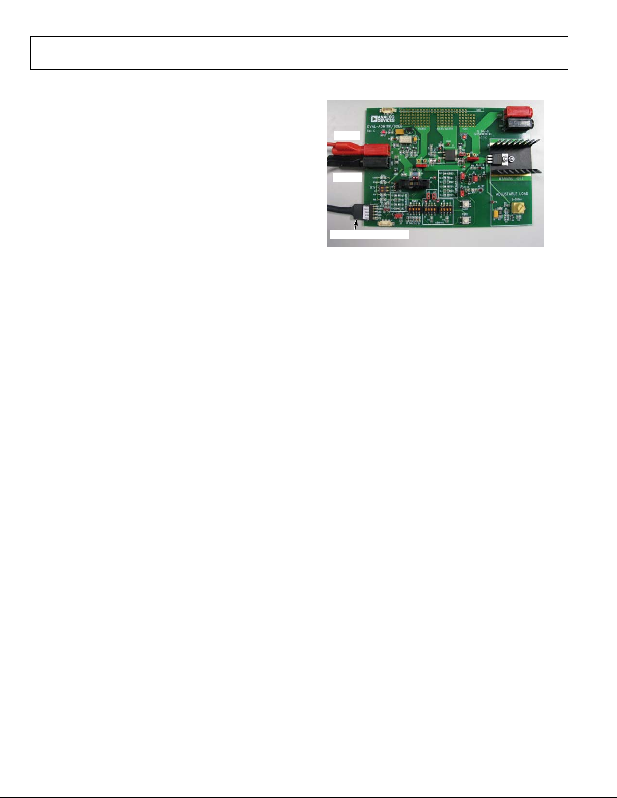
5-PIN SMBus CABLE (J7)
Figure 2. ADM1191/ADM1192 Evaluation Board
06486-002
CONFIGURATION TOOL
The evaluation kit configuration tool allows you to program
and monitor the many features of the ADM1191/ADM1192
current sense amplifiers through an intuitive GUI-based
interface. With the evaluation kit, you can verify a configuration
before using the ADM1191/ADM1192 in system applications.
The following minimum system requirements apply:
• Windows 2000
• 500 MHz processor
• 80 MB free disc space
• 256 MB RAM
• Minimum monitor resolution: 800 × 600 high color
(16 bit).
The software interface is arranged in a tabbed format, each tab
enabling the control of a key feature of the device.
Rev. 0 | Page 6 of 24
Page 7
EVAL-ADM1191/ADM1192
INSTALLING THE EVALUATION SOFTWARE
Install the ADM1191/ADM1192 software as follows:
1. Download the .zip file containing the software from
www.analog.com/powermonitorsw.
2. When the download is complete, extract the files from the
.zip file.
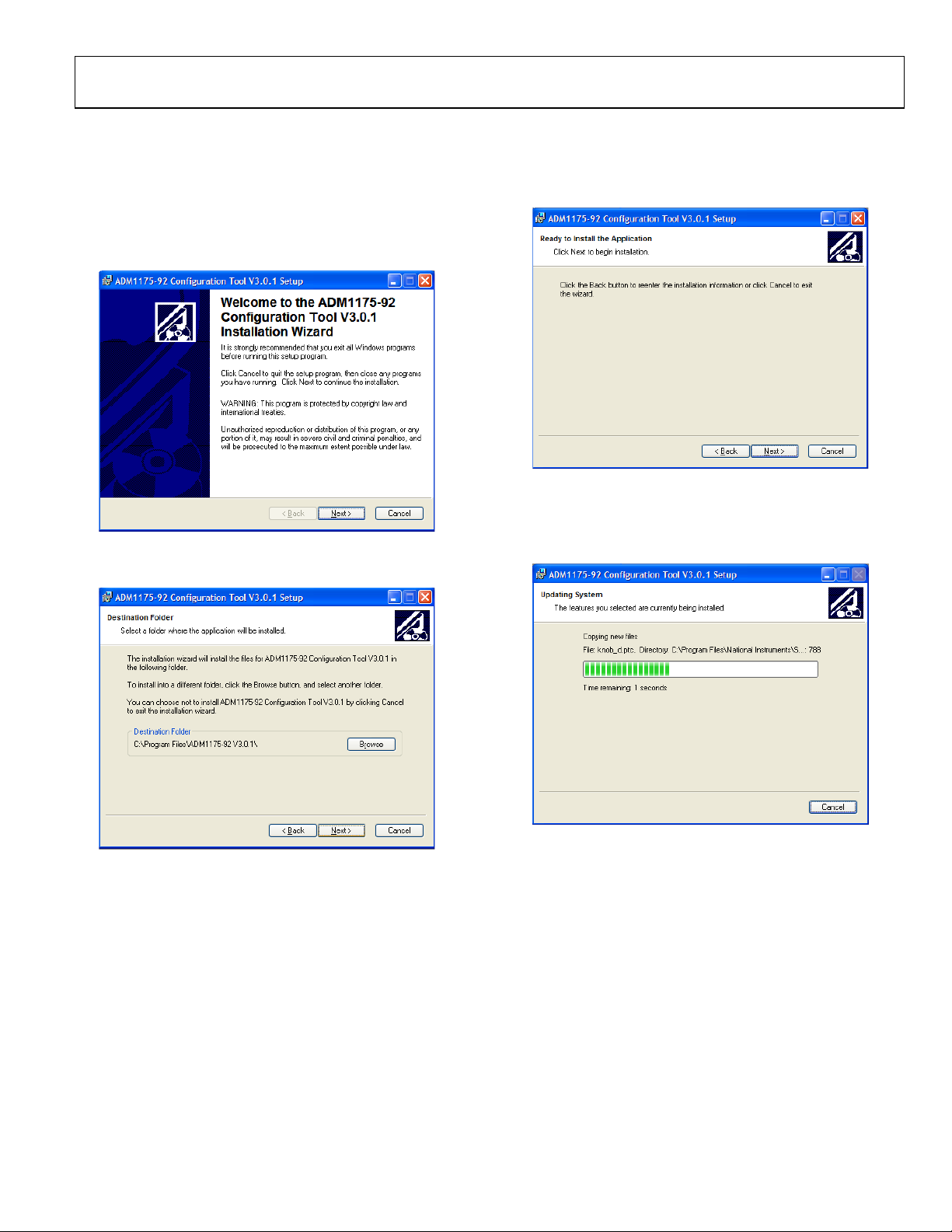
3. Double-click setup.exe. The setup window appears.
Figure 3. Evaluation Software Installation Wizard
4. Click Next to display the Destination Folder box.
06486-003
5. To create a new destination folder, click Browse. If the
default destination folder is acceptable, click Next. The
following box appears:
Figure 5. Installing the Evaluation Software
6. Choose to step back and reenter installation information,
stop installation, or begin installation. To begin installation,
click Next. The installation runs as shown in
Figure 6.
06486-005
Figure 4. Evaluation Software—Choosing a Destination Folder
06486-004
Rev. 0 | Page 7 of 24
Figure 6. Installation in Progress
06486-006
Page 8
EVAL-ADM1191/ADM1192
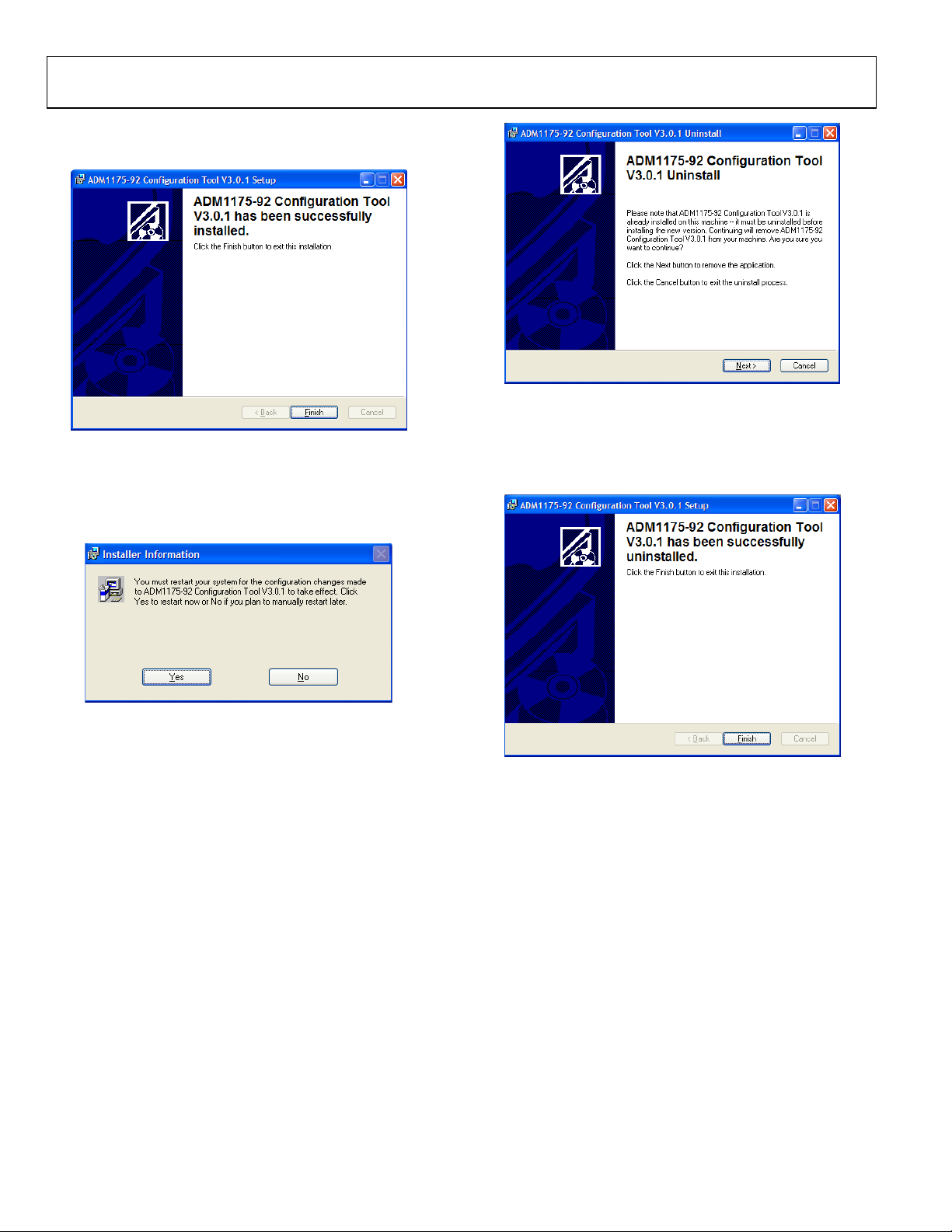
7. When installation is complete, the following message box
appears:
Figure 7. Evaluation Software—Installation Complete
8. Click Finish. The message shown in Figure 8 appears,
indicating that you must restart the system for the
configuration changes to take effect. Click Ye s to restart the
PC immediately; click No to manually restart later.
06486-009
Figure 9. Evaluation Software—Uninstalling
06486-007
When you click Next, the software uninstalls the software,
providing status as it does so, and displays the following
message to indicate that the previous version has successfully
uninstalled:
06486-008
Figure 8. Installation Restart Reminder
UNINSTALLING THE EVALUATION SOFTWARE
Before an updated version of the evaluation software is
installed, any previous version is uninstalled automatically after
the newly downloaded setup.exe is double-clicked (see Step 3).
The message shown in
previous version will be uninstalled.
Figure 9 appears, notifying you that the
Figure 10. Evaluation Software—Uninstalling Complete
MANUALLY UNINSTALLING THE EVALUATION SOFTWARE
If you want to manually uninstall the ADM1191/ADM1192
software (without upgrading it to a newer version), do the
following:
1. On the PC desktop, click Start.
2. Click Control Panel.
3. Click Add or Remove Programs.
4. Select the ADM1191 or ADM1192 program and click
Remove to uninstall it.
06486-010
Rev. 0 | Page 8 of 24
Page 9

EVAL-ADM1191/ADM1192
USB–COMMUNICATING FOR THE FIRST TIME
When the evaluation board is launched for the first time using a
USB connection, Windows does not recognize the external
board and begins installing drivers automatically. To identify
the USB converter to Windows, select the ADM1191/ADM1192
software and, when the box shown in
Install the software automatically (Recommended).
Figure 11. Automatically Installing Drivers for the Evaluation Board
In Windows XP, a warning is displayed indicating that the
hardware has not passed Windows logo testing, which verifies
compatibility with Windows XP. Because the evaluation board
has been tested and is compatible with Windows XP, you can
simply click Contine Anyway to install the necessary drivers as
shown in
Figure 12.
Figure 11 appears, select
06486-012
Figure 12. Windows XP Compatibility
After this process is complete, the message shown in Figure 13
appears. To close the installation wizard, click Finish. The
software can now be opened again and run normally.
06486-011
Rev. 0 | Page 9 of 24
Figure 13. Completing Installation
06486-013
Page 10

EVAL-ADM1191/ADM1192
STARTING THE EVALUATION SOFTWARE
1. Click Start> All Programs> ADM1175-92 Configuration
Tool 3.0.1> ADM1175-92 Configuration Tool 3.0.1 (note
that the actual folder name is version dependent).
2. When the software starts, the software agreement window
appears. Read the use conditions, select I Agree to agree
with the conditions, and click Continue.
06486-014
Figure 14. Software Agreement
If the evaluation board is powered up and an ADM1191/
ADM1192 device is in the socket, the window shown in
appears, displaying a green highlighted box that corresponds to
the device I
As shown in
2
C address.
Figure 15, there are four possible I2C addresses for
the ADM1175, ADM1177, ADM1178, and ADM1192, while
there are 16 possible I
ADM1191. In
2
C addresses for the ADM1176 and
Figure 15, an ADM1191 has responded with I2C
address 7Eh.
Figure 15
3. To c o n t inu e , cl i ck OK.
The window shown in
you are prompted to accept the sense resistor value R
(R8). The default value of the sense resistor, R
Figure 16 appears. In this example,
SENSE
, on the
SENSE
ADM1191/ADM1192 evaluation boards is 0.2 Ω.
06486-016
Figure 16. Sense Resistor Value Entry
4. Enter the value of the correct sense resistor and click OK to
continue.
Note that related information on interconnecting devices can be
found in the
Evaluating Multiple Devices in Parallel section.
06486-015
Figure 15. Device Address Detection Window
Rev. 0 | Page 10 of 24
Page 11

EVAL-ADM1191/ADM1192
EVALUATION SOFTWARE—MAIN PANEL TAB
The Main Panel tab of the evaluation software is shown in
Figure 17. It is divided into 10 control areas that you can use to
test and evaluate the ADM1191/ADM1192 devices.
Figure 17. Main Panel Tab on the User Interface
COMMAND REGISTER CONTROLS
06486-017
Alert Register controls consist of four buttons you can use to
enable or disable the various alerts generated by the device
being evaluated.
The four alert types are
• ADC OC1 (analog-to-digital converter overcurrent
Alert 1): When you enable this alert, a message box appears
prompting you to enter the current limit that triggers the
alert. When you set the sense resistor to the default value
0.2 Ω, the range is 0 to 0.529 A. If a lower value sense
resistor is used, the range increases; similarly, if a higher
value is used, the range is reduced.
Press Enter after entering the value to set it. The ADC
overcurrent alert is then triggered when a current greater
than the specified level is detected by a single ADC sample.
06486-018
Figure 18. Register Control Panel
Command Register controls allow you to manage the way in
which the device reads the data. There are five toggle buttons
with which to select the data reading method and voltage range.
The voltage range is set at 14:1 by default (7:2 if the Range
button is selected). You have the option of reading the current
and voltage just once or continuously. Once you have selected
the range and reading method, click Write D ata t o Co m ma n d
Register to pass the change to the register of the device.
Note that Read Current Once and Continuous Current Read
cannot be selected simultaneously; the same rule applies to the
voltage read buttons.
ALERT REGISTER CONTROLS
06486-019
Figure 19. Alerts Panel
06486-020
Figure 20. Analog to Digital Converter Overcurrent Alert 1
• ADC OC4 (analog-to-digital converter overcurrent
Alert 4): The ADC OC4 alert is similar to the ADC OC1
alert except that it triggers only if a current greater than the
specified level is detected for four consecutive ADC samples.
This prevents a single transient event from triggering an
ADC overcurrent condition.
• Over current Alert: This alert is enabled when an over-
current condition is present.
• OFF ALERT: This alert enables the Software Off Alert.
By default, the overcurrent alert is enabled when ADC OC1,
ADC OC4, and OFF ALERT are disabled. An enabled alert is
highlighted in yellow; a disabled alert is gray in color. To enable
or disable an alert, simply select the corresponding button in
the Alert Register.
Rev. 0 | Page 11 of 24
Page 12

EVAL-ADM1191/ADM1192
STATUS REGISTER CONTROLS
06486-021
Figure 21. Status Register
Status Register controls monitor the following alert types:
• ADC overcurrent alert
• Overcurrent alert
• Software off alert
The status register panel has six alert indicators. The upper row
shows the real-time alert status, while the lower row shows the
latched alert status. Each type of alert can be enabled or disabled
with Alert Register controls, as discussed in the
Controls
section.
To read the alert status, click Read Status Register. If the color
of an alert indicator turns from green to red, it indicates that the
alert has been triggered.
To clear latched alerts, click Clear Latched Alerts and then
click Read Status Register.
Alert Register
The Force Alert OFF control manually overrides the
ALERT/ALERTB output. The off status alert triggers when the
software turns off, and the OFF STATUS control turns from
green to red in the Status Register control panel.
OVERCURRENT OUTPUT FLAG
To the right of the Status Register controls, there is an indicator
called the Overcurrent Output Flag. For the ADM1191, it is
labeled ALERTB, while for the ADM1192, it is labeled ALERT.
This indicator updates in real time. If an overcurrent condition
is detected, the indicator changes from green to red.
06486-024
Figure 24. ADM1191 Overcurrent Output Flag
Figure 25. ADM1192 Overcurrent Output Flag
When the overcurrent condition is removed, the indicator
changes to green after Read Status Register in the Status
Register panel is selected.
Note that the positions of Jumper JP1 for the ADM1191 and
Jumper JP4 for the ADM1192 on the evaluation board affect the
status of this indicator. When the appropriate jumper is inserted
in Position A on the board, the Overcurrent Output Flag is
represented by the on-board LEDs, and the indicator in the
software is constantly green, even when an overcurrent event
occurs.
06486-025
06486-022
Figure 22. Status Register Showing Triggered Alerts
When the overcurrent alert is triggered, as shown in Figure 22,
the device goes into overcurrent protection mode. To restart the
board, cycle the power or toggle the ON pin of the device or the
software ON bit.
FORCE ALERT OFF CONTROL
06486-023
Figure 23. Software On/Off Switch
TRACE DATA DISPLAY CONTROLS
06486-026
Figure 26. Trace Data Display
The trace data display area displays the digitized current,
voltage, and power data. You have the option of changing the
name of the trace using the Trace n a m e box. The color box to
the right of the Power box indicates the color with which the
trace is plotted on the voltage, current, and power (V, I & P
graphs) tab.
When the software is supporting multiple board connections,
multiple traces appear. For more information, see the
Evaluating Multiple Devices in Parallel section.
Rev. 0 | Page 12 of 24
Page 13

EVAL-ADM1191/ADM1192
READBACK UPDATE RATE CONTROL
06486-027
Figure 27. Readback Update Rate Options
The readback update rate is set using the Readback update rate
control box shown in
Figure 27. You can choose from four
update options: every 100 ms, 200 ms, 500 ms, and 1000 ms.
Each option changes the rate at which the data in the trace data
display area is updated. The readback update rate also sets the
rate for data display in the Data Logger and the real-time
graphs on the V, I & P g r a ph s tab.
DATA LOGGER
06486-028
Figure 28. Data Logger Panel
Data Logger controls allow you to log the digitized data that is
collected to a Microsoft Excel® format file, giving you more
flexibility to monitor and compare data. You must set up the
data sampling rules. Enter the number of times to perform a
sample in the Set log limit box. If this value is zero, there is no
limit on the number of samples the data logger can log.
The sampling rate is set using one of the four options in the
Readback update rate box. In
100 samples, with 100 ms between each sample.
Figure 29, the data logger logs
CONVERT PIN CONTROL
06486-030
Figure 30. Convert Pin Control (ADM1191 Only)
The Convert Pin Control options apply to the ADM1191
device only. You can use these options to control the analog-todigital conversion of voltage and current.
Jumper JP2 should be in Position B to allow the evaluation
software to control the convert pin. If the jumper is in Position B,
the on-board switch S6 can be used to control the conversion.
The four options on the panel control the type of data conversion
carried out.
• Press to Stop Converting allows you to stop a continuous
conversion.
• Convert Once carries out a single conversion by issuing a
single pulse to the CONV pin. The result of the conversion
appears in the trace data display area at the top right of the
Main Panel tab.
• Continuously Converting begins a continuous conversion
by pulling the CONV pin high. The results of the continuous
conversion are displayed in the trace data display area.
• Pulse Convert line controls pulse frequency, as shown in
Figure 31. You can choose from one of four pulse frequencies:
100 ms, 200 ms, 500 ms, and 1000 ms.
06486-029
Figure 29. Data Logging
After you set up the data logger, click Log data to file. A file
browser box appears so that you can specify a file name and
location for storing the data. In the box, click Log to start
logging data to the file. The data is sampled at the chosen rate
and logged to the selected Excel file.
After the data begins logging, the total number of samples
logged is displayed at the bottom of the Data Logger area. This
number increases with the sampling rate. The log progress is
complete when it reaches the log limit value. Alternatively, you
can click Stop data log to file to terminate the process. After
the data is imported to the Excel file you specify, the data can be
easily evaluated.
Rev. 0 | Page 13 of 24
06486-031
Figure 31. Pulse Frequency Selection
Note that, if you set the pulse frequency for the ADM1191,
you will not be able to change the readback update rate.
Page 14

EVAL-ADM1191/ADM1192
COMMUNICATION STATUS INDICATOR
At the lower right corner of the Main Panel tab, there is a
communication status indicator that reports the status of the
connection between the software and the evaluation board.
There are three possible indicators, as shown in
Figure 32. Device Communication Indicator
Figure 32.
06486-032
The leftmost indicator reports normal communication. The
middle indicator spins to report a write data to register. The
third indicator reports that communication between the device
and the user interface has been lost. The software should be
restarted to reestablish communication with the device.
Rev. 0 | Page 14 of 24
Page 15

EVAL-ADM1191/ADM1192
REAL-TIME GRAPHS OF VOLTAGE, CURRENT, AND POWER
On the V, I & P g ra ph s tab, you can monitor data collected
through the evaluation board using the software generated
graphs. On the tab, there are three sets of controls and graphs
corresponding to voltage, current, and power. Voltage and
current graphs are displayed using actual voltage and current
data from the device. The values for the power graph are
calculated using P = V.I.
06486-033
Figure 33. Panel Selection Tabs
The Readback update rate control on the Main Panel tab sets
the rate at which the ADC samples are taken and, consequently,
the speed at which the graphs update.
format. The options are Strip Chart, Scope Chart, and Sweep
Chart. The default is Scope Chart.
06486-037
Figure 37. Pause Graph and Chart Type Selection
Figure 38 shows the result of varying the supply voltage. Note
that the power graph also changes.
06486-034
Figure 34. Voltage, Current, and Power Plot
The digitized values for voltage, current, and power are displayed at
the left in each set of controls and graphs.
06486-035
Figure 35. Trace Identifier
For ease of viewing, you can scale the y-axis of a plot.
06486-036
Figure 36. Scale Adjustment Bar
At the top right corner of the tab, there is a Pause button that
you can use to pause the graph from real-time plotting. There is
also a chart selection box that you can use to choose a graph
Figure 38. Plot with Voltage Variation
Figure 39 shows that the supply voltage is constant but that the
current is changing as a result of varying the load resistance by
turning switch VR1. Turning VR1 clockwise reduces the load
resistance, thereby increasing the current; turning VR1
counterclockwise has the opposite effect. Again, notice the
variation in the power graph as the current graph changes.
Figure 39. Plot with Current Variation
06486-038
06486-039
Rev. 0 | Page 15 of 24
Page 16

EVAL-ADM1191/ADM1192
EVALUATING MULTIPLE DEVICES IN PARALLEL
For the ADM1191, up to 16 unique I2C addresses can be created,
allowing you to interconnect up to 16 devices. For the ADM1192,
up to four I
connect up to four ADM1192 devices.
Each evaluation board is fitted with switches labeled A0 and A1.
A0 is used on an ADM1192 device to assign an address, via the
ADR pin, to that particular device. For the ADM1191, both A0
and A1 are used to assign up to 16 I
ensure that each device has a unique I
When interconnecting ADM1191/ADM1192 devices, you should
power each device using a bench supply of between 3.15 V and
26 V, connected to J2 (VIN) and J4 (GND).
The first evaluation board should be connected to the PC
parallel port using a 5-pin SMBus cable from the 5-pin header
labeled J7. Each board is fitted with two Minimolex connectors,
J1 and J5. To interconnect multiple boards, use the red 5-pin
Minimolex cables provided.
COMMUNICATING WITH INTERCONNECTED ADM1191/ADM1192 EVALUATION BOARDS
Figure 40 displays the result of the device address search when
two ADM1191s, one ADM1192, and one ADM1176 are
cascaded. Note that the I
highlighted in green.
2
C addresses can be created, allowing you to inter-
2
C addresses. You must
2
C address.
2
C addresses of the four devices are
Figure 41. Sense Resistor Value Input Panel for Multiple Devices
Click OK to proceed. The evaluation software Main Panel tab
appears.
06486-041
Figure 40. Device Address Search for Four Interconnected
ADM1191/ADM1192 Devices
After you click OK, the window shown in Figure 41 appears,
prompting you to enter the value of the current sense resistors.
The default value of the sense Resistor, R8, is 0.2 Ω.
06486-042
Figure 42. Main Panel for Multiple Devices
Note the Device selector drop-down box at the top of the tab.
06486-043
Figure 43. Multidevice Selector
06486-040
You can use this box to select each device and select the configuration settings for that device. After you select the range and
reading methods, click Write Data to Command Register in
the Command Register control panel to pass the changes to the
device register.
Rev. 0 | Page 16 of 24
Page 17

EVAL-ADM1191/ADM1192
You can view the voltage, current, and power graphs on the
V, I & P g r a p h s tab.
06486-046
06486-047
Figure 44. Voltage, Current, and Power Plot for Multiple Devices
The digitized values for voltage, current. and power are displayed at the left in each set of controls and graphs. You can
select the traces to view by clicking the box to the left of each
trace name. You can also scale the y-axis of the plots for easy
viewing.
Figure 45 depicts the result of altering the input voltage. Note
the corresponding change on the power graph.
Figure 46. Multidevice Plot with Current Variation
06486-044
If more than four boards are interconnected, there are
additional tabs for the voltage, current, and power graphs. As
shown in
Figure 47, four traces are displayed in each graph, up
to a maximum of 16 traces on four graph tabs when 16 ADM1191
devices are set up in parallel.
Figure 47. Multidevice Panel Selection Tab
06486-045
Figure 45. Plot with Voltage Variation for Multiple Devices
As shown in Figure 45, the supply voltage is constant and the
current associated with traces is varied. The current is changed
by changing the load resistance. Turning VR1 clockwise on each
evaluation board reduces the load resistance, thereby increasing
the current, and turning VR1 counterclockwise increases the
load resistance and, thus, reduces the current.
Rev. 0 | Page 17 of 24
Figure 48. Multidevice Plotting Screen for Device 1 Through Device 4
06486-048
Page 18

EVAL-ADM1191/ADM1192
INTERCONNECTING A COMBINATION OF ADM1191 AND ADM1192 DEVICES
ALERT/ALERTB output is not supported by the evaluation
tool when a combination of ADM1191 and ADM1192 devices
is interconnected. This is because the ADM1191 and ADM1192
have alert outputs with opposing polarity (ALERTB and
ALERT), and these output flags cannot be supported as a single
logic signal via J7 through J5 to the PC.
06486-049
Figure 49. Overcurrent Flag Indicator for Interconnected Devices with ALERT
and ALERTB Output
The Main Panel tab of the configuration tool has a different
appearance in this situation. To the right of Status Register,
there is no Overcurrent Output Flag for either the ADM1191
or the ADM1192 device.
Note that the Overcurrent Output Flag appears when
ADM1178 and ADM1191 devices are interconnected. The
reason is that both devices have the ALERTB type output.
Therefore, when interconnecting a combination of ADM1191
and ADM1192 devices, it is recommended that you use the
LEDs on the evaluation board that correspond to ALERT (D1)
and ALERTB (D5) to give a hardware alert. When an overcurrent condition is detected, the corresponding LED lights up.
To configure the evaluation board to give a hardware alert for
ALERT/ALERTB, position the jumpers as shown in
Tabl e 6.
Table 6. Jumper Positions for ALERT/ALERTB
Device Jumper
ADM1191 JP1 Position A
ADM1192 JP3 Position B
ADM1192 JP4 Position A
Note that, if an overcurrent condition occurs for the ADM1192,
you can press the on-board CLRB button to clear the alert after
the overcurrent condition is eliminated. This does not apply to
the ADM1191.
Rev. 0 | Page 18 of 24
Page 19

EVAL-ADM1191/ADM1192
EVALUATION BOARD SCHEMATIC
06486-050
Figure 50.
Rev. 0 | Page 19 of 24
Page 20

EVAL-ADM1191/ADM1192
ORDERING INFORMATION
BILL OF MATERIALS
Table 7.
Reference
Designator
Qty
1 C1
1 C2
1 C3
2 C4, C5 User-defined capacitor
5
C6, C10, C11, C12,
C17
1 C7
1 C9
1 C13
2 C15, C16 10 pF, 5%, 0603, multilayer ceramic capacitor Epcos B37930K5100J60 FEC 9753478
4 D1, D3, D4, D5 LED-0805, red SMD LED Avago HLMP-6000-E0011 FEC 1003354
1 D2 3.3 V, 5%, SOT23, Zener diode Philips BZX84-C3V3 T/R FEC 1081419
1 D6 10 V, DIODE-SMB, Zener diode Philips BZV55-C10 FEC 1081361
2 J1, J5
2 J2, J3 Red 4 mm banana Deltron 571-0500-01 FEC 1101127
1 J7 MOLEX, 5-way right angle header Molex 22-12-2054 FEC 3116890
2 J8, J10
2 J9, J4 Black 4 mm banana socket Deltron 571-0100-01 FEC 1101128
7
JP1, JP2, JP3, JP4,
JP5, JP6, JP7
1 P10 TO220 heat sink AAVID Thermalloy TV40 FEC 170074
1 Q1
4 Q2, Q3, Q4, Q7
1 Q5
2 Q6, Q8
1 R1 22 kΩ, 1%, 0805, SMD resistor Multicomp MC 0.1W 0805 1% 22K FEC 9332820
9
R2, R6A, R7, R9, R22,
R25, R27, R28, R29
2 R3, R4 2.2 kΩ, 1%, 0805, SMD resistor Multicomp MC 0.1W 0805 1% 2K2 FEC 9332812
1 R5 1 MΩ, 1%, 0805, SMD resistor Multicomp MC 0.1W 0805 1% 1M FEC 9332413
1 R5A 3.3 kΩ, 1%, 0805, SMD resistor Multicomp MC 0.1W 0805 1% 3K3 FEC 9333045
1 R8 0.2 Ω, 1%, 2512, current sense SMD resistor Welwyn LR2512-R20FW FEC 1100068
2 R10, R11 1.8 kΩ, 0805, SMD resistor Multicomp MC 0.1W 0805 1% 1K8 FEC 9332715
2 R12, R13 150 kΩ, 1%, 0805, SMD resistor Multicomp MC 0.1W 0805 1% 150K FEC 9332626
Description Manufacturer
4.7 nF, 10%, 0805,
capacitor
47 nF, 10%, 0805,
capacitor
470 nF, 10%, 0805,
capacitor
0.1μF, 10%, 0805,
capacitor
10 μF, 10%, CAP\TAJ_D, 35 V Tantalum
capacitor
100 μF, 10%, CAP\TAJ_C, 10 V Tantalum
capacitor
10 μF, 10%, CAP\TAJ_A, 10 V Tantalum
capacitor
MOLEX53398-0671, 6-way SMD straight mini
header
PCB_SELECTOR_PLUGS_DIP4, 4-pin (2 x 2)
shorting and socket
LINK-3P, 3-pin (0.1" pitch) header and jumper
socket
IRFR_U3910_TRIPLE_FOOTPRINT, MOSFET, P,
D2-PAK
BC849BLT1G, SOT23, NPN small signal
transistor
TO-220_EXPOSED_PAD_HEATSINK, MOSFET,
N logic
SOT23, N-channel, enhancement mode,
TMOSFET
1 kΩ, %, 0805, SMD resistor Multicomp MC 0.1W 0805 1% 1K FEC 9332383
multilayer ceramic
multilayer ceramic
multilayer ceramic
multilayer ceramic
Phycomp 2238 580 15632 FEC 3019913
Phycomp 2238 580 15645 FEC 718683
Multicomp B0805R474KCT FEC 9406336
Multicomp U0805R104KCT FEC 9406387
Kemet T495D106K035ATE300 FEC 9229248
AVX TAJC107K010R FEC 197180
AVX TPSA106K010R1800 FEC 1135105
Molex 533980671–Molex FEC 1125368
Harwin
Harwin
Vishay SUB65P06-20 FEC 9551395
On Semiconductor BC849BLT1G FEC 9558616
Fairchild FDP7030BL FEC 9845151
Fairchild NDS7002A FEC 9845437
Manufacturer
Number
D3086-98 & H316101/ D3086-98
M20-9990346/
M7566-05
Supplier
Number
FEC 149318/
149306
FEC 1022249/
150411
1
Rev. 0 | Page 20 of 24
Page 21

EVAL-ADM1191/ADM1192
Reference
Qty
Designator Description Manufacturer
1 R14A 2.4 kΩ, 1%, 0805, SMD resistor Multicomp MC 0.1W 0805 1% 2K4 FEC 9332880
2 R15, R17 100 kΩ, 1%, 0805, SMD resistor Multicomp
1 R16 510 Ω 1%, 0805, SMD resistor Multicomp MC 0.1W 0805 1% 510R FEC 9333312
1 R18 100 Ω 1%, 0805, SMD resistor Multicomp
1 R19 3 kΩ,1%, 0805, SMD resistor Multicomp MC 0.1W 0805 1% 3K FEC 9332995
1 R20 10 Ω, 1%, 0805, SMD resistor Multicomp MC 0.1W 0805 1% 10R FEC 4762113
1 R21 1 Ω, 5, 0805, SMD resistor Phycomp 232276260108 FEC 9235833
1 R23 13.3 kΩ, 5, SMD resistor Yageo RC0805FR-0713K3L
1 R24 47 kΩ, 0805, SMD resistor Multicomp MC 0.1W 0805 1% 47K FEC 9333274
1 R26A 3.3 Ω, 1%, 0805, SMD resistor Multicomp MC 0.1W 0805 1% 3K3 FEC 9333096
1 RL1 RELAY-IM02GR, SMD DPCO 4.5VDC, relay Tyco IM02GR FEC 4148344
1 S1
SW\2_DIP_SMD, DIP4_SMD, 2-way SMD
Omron A6S-2102 FEC 9901850
switch
3 S2, S3, S4 SW\4DIP, DIP8_SMD, 4-way SMD switch Omron A6S-4101 FEC 9901868
2 S5, S6
SW-PUSH-SMD, SW_PB_SMD_6MM, SMD
Omron B3S-1000 FEC 177807
push button switch (sealed)
13
DRAIN, GATE,
Red testpoint Vero 20-313137 FEC 8731144
SOURCE, TP1, TP2,
TP3, TP4, TP5, TP6,
TP7, TP8, TP11,
TP12
2 TP13, TP14 Black testpoint Vero 20-2137 FEC 8731128
1 U1 MSO10 Analog Devices ADM1191ARMZ/
1 U2 TO-92C, 3.3 V regulator STMicroelectronics LE33CZ FEC 9755349
1 U3 MSO10-SKT, 10-pin MSOP socket Wells 656-0102211
1 VR1 VRES_ROTARY, trimmer pot Vishay Spectrol 63M-T607-202 FEC 9608214
4
R5B, R6B, R14B,
User-defined resistor
R26B
4 Stick-on feet 3M FEC 148-922
1
FEC indicates the Farnell Electronic Components company.
ORDERING GUIDE
Model Description
EVAL-ADM1191EBZ
EVAL-ADM1192EBZ
CABLE-SMBUS-5PINZ
USB-5PSMBUS-CABLEZ
1
Z = RoHS Compliant Part.
1
1
1
ADM1191 Evaluation Board
ADM1192 Evaluation Board
5-Pin SMBus Cable (Parallel Port)
1
5-Pin SMBus Cable (USB Port)
ESD CAUTION
Manufacturer
Number
MC 0.1W 0805 1%
100K
MC 0.1W 0805 1%
100R
ADM1192ARMZ
Supplier
Number
1
FEC 9332405
FEC 9332375
Digikey 311-
13.3KCRCT-ND
Abrel Products
656-0102211
Rev. 0 | Page 21 of 24
Page 22

EVAL-ADM1191/ADM1192
NOTES
Rev. 0 | Page 22 of 24
Page 23

EVAL-ADM1191/ADM1192
NOTES
Rev. 0 | Page 23 of 24
Page 24

EVAL-ADM1191/ADM1192
NOTES
Purchase of licensed I2C components of Analog Devices or one of its sublicensed Associated Companies conveys a license for the purchaser under the Philips Rights to
use these components in an I2C system, provided that the system conforms to the I2C Standard Specification as defined by Philips.
©2008 Analog Devices, Inc. All rights reserved. Trademarks and
registered trademarks are the property of their respective owners.
EB06486–0–5/08(0)
Rev. 0 | Page 24 of 24
 Loading...