

现货库存、技术资料、百科信息、热点资讯,精彩尽在鼎好!
PRELIMINARY TECHNICAL DA T A
Evaluation Board Documentation
a
Preliminary Technical Data
FEATURES
Single +5 V Power Supply
Easy Connection of External Transducers via Screw
Terminals
Easy Modification of Signal Conditioning Components
Using PCB Sockets
Trim Pot for Analog Calibration of Meter Constant
Optically Isolated Output for Calibration/Test Purposes
External Reference Option Available for Reference
Evaluation
ADE7757 Energy Metering IC
EVAL-ADE7757EB
GENERAL DESCRIPTION
The ADE7757 is a high accuracy energy measurement IC
with integrated oscillator. The part specifications surpass
the accuracy requirements as quoted in the IEC1036 standard.
The ADE7757 supplies average real power information on the
low frequency outputs F1 and F2. These logic outputs may be
used to directly drive an electromechanical counter or interface
to an MCU. The evaluation board provides screw connectors
for easy connection to an external counter. The CF logic output gives instantaneous real power information. This output is
intended to be used for calibration purposes. The evaluation
board allows this logic output to be connected to an LED or
optoisolator.
The ADE7757 evaluation board can easily be converted into
an energy meter by the addition of a local power supply and
the connection of the appropriate current sensor. A large
amount of prototype area is made available on the evaluation
board for this purpose.
V2P
V2N
V1N
V1P
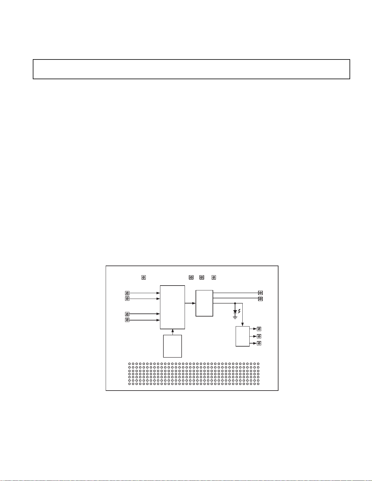
FUNCTIONAL BLOCK DIAGRAM
VCC
AGND
ADE7757
AD780
VDD
74HC08
PROTOTYPE
AREA
DGND
CF
H11L1
F1
F2
VPLUS
CFOUT
VMINUS
REV. PrF
Information furnished by Analog Devices is believed to be accurate and
reliable. However, no responsibility is assumed by Analog Devices for its
use, nor for any infringements of patents or other rights of third parties
which may result from its use. No license is granted by implication or
otherwise under any patent or patent rights of Analog Devices.
One Technology Way, P.O. Box 9106, Norwood, MA 02062-9106, USA
Tel: 781/329-4700 www.analog.com
Fax: 781/326-8703 © Analog Devices, Inc., June 2002
EVAL-ADE7757EB
PRELIMINAR Y TECHNICAL DA T A
ANALOG INPUTS (SK1 AND SK2)
Voltage and current signals are connected at the screw terminals SK1 and SK2 respectively. All analog input signals are
filtered using the on-board antialias filters before being presented to the analog inputs of the ADE7757. Some analog
inputs offer additional signal conditioning, e.g., attenuation on
the voltage channel. The default component values included
with the evaluation board are the recommended values to be
used with ADE7757. The user can easily change these components, but this is not recommended unless the user is familiar
with sigma-delta converters as well as the criteria used for selecting the analog input filters—see ADE7757 datasheet.
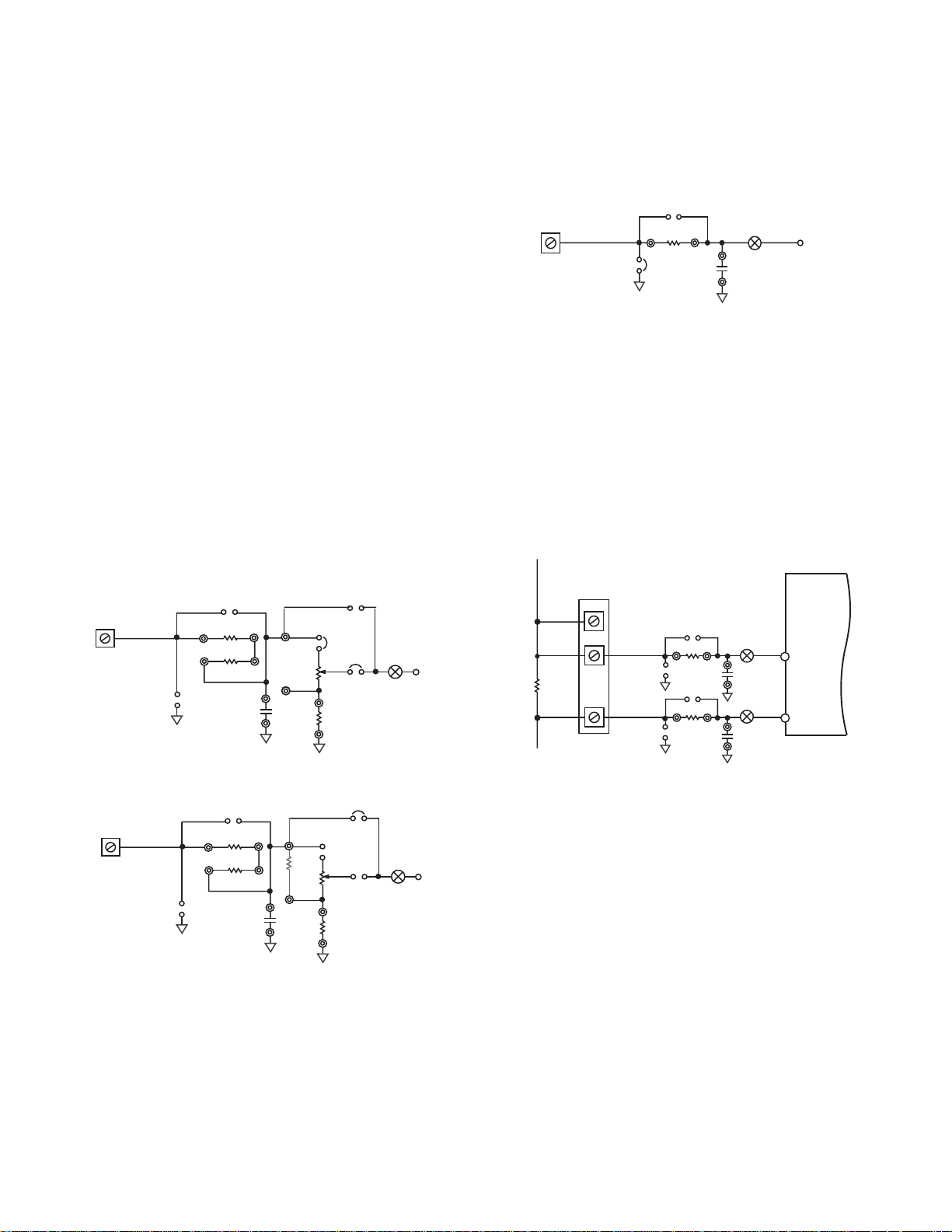
Voltage Input
SK2 is a two-way connection block that can be directly
connected to a high voltage source, e.g., 220 V rms. The
resistor network R15 (trim pot), R19, R20, R21, and R22
make up a very flexible attenuation and calibration network—see schematic. The attenuation network is designed
such that the corner frequency (–3 dB frequency) of the
network matches that of the RC (antialiasing) filters on
the other analog inputs. This is important, because if they
do not match there will be large errors at low power factors. Figure 1 shows how the attenuation network may be
used with fixed resistors or the trim pot. The trim pot
allows the voltage signal on V2P to be scaled to calibrate
the frequency on CF to some given constant, e.g., 100
imp/kWhr. Some examples are given later.
If Channel 2 is being used in a single-ended mode of operation, the unused input of the pair should be connected
to analog ground (AGND) via an antialias filter. This is
shown in Figure 2 where V2N is connected to AGND
using jumper JP8.
JP7
SK2B
R18
JP8
TP5
V2N
C19
Figure 2. Unused Analog Inputs Connected to AGND
All passive components (resistors and capacitors) which
make up the attenuation network and antialias filters may
be modified by the user. The components are mounted using
PCB jack sockets for easy removal and replacement of
components.
Current Input
SK1 is a two-way connection block, which allows the
ADE7757 to be connected to a current sensor through one
differential input channel. In this example, we chose a shunt as
the current sensor. Figure 3 shows a typical connection diagram for shunt connection.
JP5
SK2A
R19
R20
JP6
JP18
R21
R15
C18
a. Attenuation Using Trim Pot (R15)
JP5
SK2A
JP6
R19
R20
R21
R15
C18
b. Attenuation Using Fixed Resistors
Figure 1. Attenuation Network on Channel 2
JP18
R22
R22
B
JP17
A
JP17
SK1A
SK1B
V2P
B
SHUNT
SK1C
Figure 3. Typical Shunt Connection for Channel 1
AGND
JP2
JP4
JP1
R16
JP3
R17
TP1
C16
TP2
C17
ADE7757
V1N
V1P
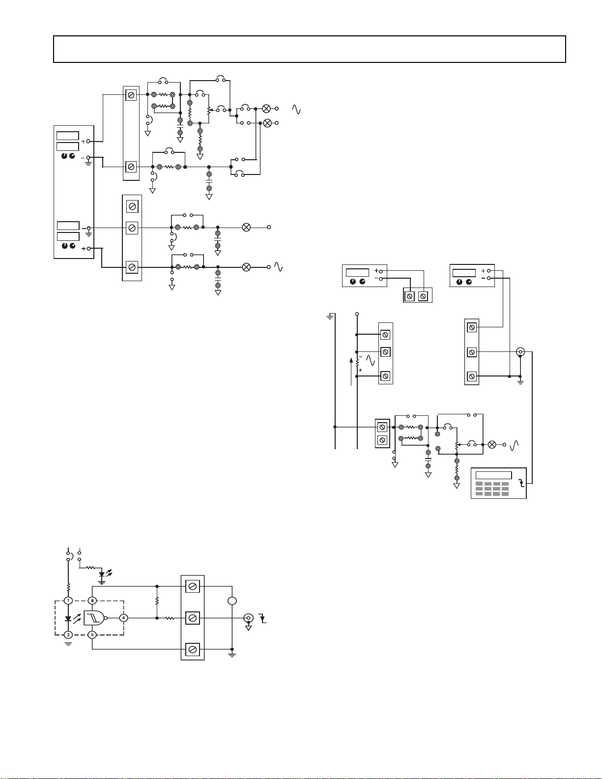
EVALUATION BOARD SETUP (ANALOG INPUTS)
Figure 4 shows how the ADE7757 evaluation board can be set
A
V2P
up for a simple evaluation. Two signal generators are used to
provide the sinusoidal (ac) signals for Channel 1 and Channel
2. The user must have some way of phase locking the generators. Also if the ADE7757 performance-over-power factor is
being evaluated, two separate signal sources will be required.
The generators are shown connected in a single-ended configuration. The grounded analog inputs of Channel 1 and Channel
2 (V1N and V2N) are connected to AGND via an antialias
filter. In Figure 4, analog input V2N is grounded via R21 and
R22. The capacitor C18 is connected in parallel.
–2–
REV. PrF
PRELIMINARY TECHNICAL DA T A
EVAL-ADE7757EB
JP5
A
50Hz
220V
50Hz
30mV
SK2A
SK2B
SK1A
SK1B
SK1C
R19
R20
JP6
JP8
AGND
C18
JP7
R18
JP2
JP4
JP1
R16
JP3
R17
JP18
R21
R15
R22
JP17
C19
P
TP4
B
N
JP16
P
N
JP9
TP1
C16
TP2
C17
V2P
V2N
TP5
V1N
V1P
Figure 4. Typical Connection for Analog Inputs
LOGIC OUTPUTS
ADE7757 provides the active power information in the
form of an output frequency. The three frequency outputs
are F1, F2 and CF. Consult the datasheet for more information on these outputs. The logic outputs F1 and F2 are
intended to be used to drive an impulse counter or stepper
motor. The outputs are buffered and available at the connector SK6. A stepper motor may be directly connected
here. The power supply for the buffer is +5V (SK4A) and
may be connected to the ADE7757 supply using jumper
JP15, or to its own supply.
The logic output CF can be directly connected to an LED
using JP14 (Position B) or to an optically isolated output (Position A). By closing Positions A and B, both options are selected. The optically isolated output is available at connector
SK5. This isolated output is useful when the evaluation board
is connected directly to a high voltage (e.g., 220 V residential). A
typical connection diagram for this isolated output is shown in
Figure 5.
JP14
B
A
R11
OUTPUT FREQUENCY SELECTION
ADE7757 provides up to four different output frequencies
on F1 and F2. The output frequency selection is made via
the logic inputs S0 and S1—see ADE7757 datasheet. On
the evaluation board these inputs are set by using jumpers
JP12 and JP13. The logic input SCF is set via jumper 11
(JP11). For a full explanation of the ADE7757 output
frequency selection see the datasheet.
INTERNAL CLOCK
The ADE7757’s integrated oscillator serves as the clock
source to the chip. A precise 6.2 k
Ω
resistor with low
tolerance and low drift is used to drive the internal oscillator.
NEUTRAL
SHUNT
5.000V
PHASE
220V
SK1A
SK1B
5A
2mV
SK1C
SK2A
SK2B
LOAD
JP1 = OPEN
JP2 = OPEN
JP3 = OPEN
JP4 = OPEN
JP5 = OPEN
JP6 = OPEN
JP7 = OPEN
JP8 = CLOSED
JP9 = N
SK3A
VDD
AGND
AGND
V1N
V1P
JP5
R19
R20
JP6
C18
JP11 = 1
JP12 = 1
JP13 = 0
JP14 = A,B
JP16 = P
JP17 = A
JP18 = CLOSED
R21 = REMOVED
SK3B
R21
5.000V
JP18
R15
R22
SK5A
SK5B
SK5C
B
JP17
A
TP4
V2
54.5mV
0.9776 Hz
FREQUENCY DISPLAY
100
imp/kWhr
R12
U4
H11L1
VPLUS
CFOUT
VMINUS
R4
R5
SK5A
SK5B
SK5C
+
5V to 12V
COUNTER
Figure 5. Typical Connection for Opto Output
All logic outputs can be monitored via test points 6 to 8
(TP6 to TP8). These test points provide easy access for
scope probes and meter probes.
REV. PrF
Figure 6. ADE7757 Evaluation Board as an Energy Meter
EVALUATION BOARD SET UP AS AN ENERGY
METER
Figure 6 shows a wiring diagram that allows a simple
energy meter to be implemented using the ADE7757
evaluation board. The current transducer used in this ex-
Ω
ample is a 400 µ
shunt. The meter is intended to be used
with a line voltage of 220 V and a maximum current of
25 A. The frequency outputs F1 and F2 can be used to
drive a mechanical counter. These outputs will be calibrated to provide 100 imp/kWhr. The logic output CF
has an output frequency that can be up to 2048 times higher
–3–

EVAL-ADE7757EB
PRELIMINAR Y TECHNICAL DA T A
than the frequency on F1 and F2. This output can be used
for calibration purposes and is shown connected to a frequency counter via the optoisolator in Figure 6.
At maximum current (25 A), the power seen by the meter
will be 5.5 kW. This will produce a frequency of 0.153 Hz
on F1 and F2 when these outputs are calibrated to
100imp/kWhr (100imp/hr = 0.02777 Hz, 0.02777 x 5.5 =
0.153 Hz). From Table V in the ADE7757 datasheet, the
closest frequency to 0.153 Hz in the half-scale ac inputs
column is for F
tor frequency of 466k Hz. Therefore F
ting S1 = 1 and S0 = 0. The choice of CF frequencies in
this mode (see Table III in the ADE7757 datasheet) are
32 times F1 and 16 times F1. For this example 32 times
F1 is selected by setting SCF = 1.
Since the voltage on Channel 1 is fixed, the only possible
way of calibrating (adjusting) the output frequency in F1
and F2 is by varying the voltage on Channel 2. This is
carried out by varying the attenuation of the line voltage
using the trim pot.
First we can calculate the voltage required in Channel 2 in
order to calibrate the frequency on the logic outputs F1 and F2
to 100imp/kWhr. The ADE7757 datasheet gives the equation
which relates the voltage on Channel 1 and Channel 2 to the
output frequency on F1 and F2.
First a current is selected for calibration, 5 A for example.
This gives a Channel 1 voltage of 400 µ
rms. The on-chip or external reference of 2.5 V is selected
using JP10.
The output frequency at 5 A on F1 and F2 should be
(100imp/kWhr) x 1.1 kW = 0.03055 Hz, where (220 V x
5 A = 1.1 kW).
From Equation 1 the voltage on Channel 2 should be set
to 54.4 mV. The attenuation network as shown in Figure
1 is used to attenuate 220 V to 54.4 mV. R19 = 590 k
R20 = 200 k
However, since the meter is being calibrated at CF and
CF is set to 32 times F1, the voltage on Channel 2 should
be adjusted until CF = 32 x 0.03055 Hz = 0.9776 Hz is
registered on the frequency counter. The counter should
be set up to display the average of ten frequency measurements on CF. This will remove any ripple due to the
instantaneous power signal. See the ADE7757 datasheet
for more details.
JUMPER SELECTION
The ADE7757 evaluation board comes with several
jumper selections that allow the user to exercise all of
the ADE7757 functionality. There are also some options
such as attenuation networks and optically isolated outputs
that allow the ADE7757 to be evaluated under the same
conditions as the end application. Table I outlines all the
jumper options and explains how they are used. Table I
should be used in conjugation with Figure 7, which will
make it easier to locate the jumper in question.
, i.e., 0.18 Hz for a nominal internal oscilla-
3
84515
.
=
Freq
Ω,
R22 = 100Ω and the trim pot R15 =100Ω.
2
V
is selected by set-
3
×××
FVV
4121
−
ref
Ω
x 5 A = 2 mV
Ω
(1)
,
–4–
Table I.
Jumper Option Description
JP1 Closed Closing this jumper will short resistor
R16 and connect analog input V1N
directly to SK1B. This has the effect
of removing the antialias filter from
this input.
Open Antialias filter in input V1N is en-
abled.
JP2 Closed Analog input V1N is connected to
analog ground (AGND) via the
antialias filter. This jumper should be
closed if the Channel 1 is used in a
single-ended mode.
Open When evaluating the ADE7757, Chan-
nel 1 is best used in a differential
mode and this jumper should be left
open. An example is shown in Figure
3. In this example a shunt is used to
sense the current. The shunt can be
referenced to the AGND of the board
by using TP9 as shown.
JP3 Closed Closing this jumper will short resistor
R17 and connect analog input V1P
directly to SK1C. This has the effect
of removing the antialias filter from
this input.
Open Antialias filter in input V1P is enabled.
JP4 Closed Analog input V1P is connected to ana-
log ground (AGND) via the antialias
filter.
Open Normal operation.
JP5 Closed Closing this jumper will short resistors
R19 and R20. The analog input V2P is
connected directly to SK2A. This has
the effect of removing the antialias
filter/attenuation network from this
input. Note: if the board is being connected to a high voltage, this jumper
must be left open.
Open Antialias filter/attenuation network on
the input V2P is enabled.
JP6 Closed Analog input V2P is connected to ana-
log ground (AGND) via the antialias
filter/attenuation network. Note: SK2A
is also connected to AGND. Be careful when connecting this input a high
voltage source.
Open Normal operation.
JP7 Closed Closing this jumper will short resistor
R18 and connect analog input V2N
directly to SK2B. This has the effect
of removing the antialias filter/attenuation network from this input.
Open Antialias filter/attenuation network in
input V2N is enabled.
REV. PrF

PRELIMINARY TECHNICAL DA T A
JP8 Closed Analog input V2N is connected to
analog ground (AGND) via the
antialias filter/attenuation network.
This option should be selected if
Channel 2 is used in a single-ended
mode.
Open V2N connected to SK2B for differential
operation.
JP9 N SK2B connected to V2N.
P SK2B connected to V2P.
JP10 Open ADE7757 internal (on-chip) reference
selected.
Closed External (AD780) reference selected.
JP11 1 SCF connected to VDD.
0 SCF connected to DGND.
JP12 1 S1 connected to VDD.
0 S1 connected to DGND.
JP13 1 S0 connected to VDD.
0 S0 connected to DGND.
JP14 A CF logic output connected to optically
isolated output at SK5.
B CF logic output connected to LED.
JP15 Closed VDD and +5V connected together.
Note: VDD is power supply for
ADE7757 IC (U1) and +5V is power
supply for buffer (U2)
JP16 N SK2A connected to V2N.
P SK2A connected to V2P.
JP17 A Trim pot R15 is connected to V2P or
V2N (depending on the position of
JP16)—see Figure 8. This allows the
output frequency to be scaled using the
voltage on V2P.
B When option B is selected, the jumper
JP18 should be left open. In this configuration the attenuation for V2P is
provided via the fixed resistors R19,
R20, R21 and R22.
JP18 Open When open, the attenuation on V2P is
provided by fixed resistor as explained
above. Also see Figure 10.
Closed When closed, the trim pot becomes
part of the attenuation network. In this
mode of operation, the resistor R21
should be removed from its PCB jack
sockets and JP17B must be opened
EVAL-ADE7757EB
REV. PrF
–5–

EVAL-ADE7757EB
PRELIMINAR Y TECHNICAL DA T A
Figure 7. ADE7757 Evaluation Board Jumper Positions
–6–
JUMPER OPEN
JUMPER CLOSED
REV. PrF

PRELIMINARY TECHNICAL DA T A
EVAL-ADE7757EB
Evaluation Board Bill of Material
Designator Value Description
R1, R2, R3, R4 1 k
R5 100
R7, R8, R9 10 k
R11, R12 820
R13, R14 20
R15 100
R16, R17, R18 200
R19 402 k
R20 200 k
R21, R22 100
C1 1 µF, 10% 16V Voltage reference decoupling capacitor.
C2, C3, C4 10 µF, 10% 16V Power supply decoupling capacitors, 20%, Philips CW20C 104,
C5 6.2 k
C7, C8, C9, C10, C11, 100 nF, 10% 100 V Power Supply Decoupling Capacitors, 10%, X7R type, AVXC12, C20 KYOCERNA, FARNELL Part No. 146-227.
Ω
, 5%, 1/4 W Resistor, No Special Requirements.
Ω
, 5%, 1/4 W Resistor, No Special Requirements.
Ω
, 5%, 1/4 W Resistor, No Special Requirements.
Ω
, 1%, 1/4 W Resistor, No Special Requirements.
Ω
, 5%, 1/4 W Resistor, No Special Requirements.
Ω
, 10%, 1/2 W Trim Pot Resistor, 25 Turn.
BOURNS.
Ω
, 0.05%, 1/8 W ±15 ppm/°C Resistor, good tolerance, used as part of the analog filter
network. These resistors are not soldered, but are plugged into PCB
mount sockets for easy modification by the customer. Low drift
WELWYN RC6 Series, FARNELL Part No. 339-179.
Ω
, 1%,1/4 W ±50 ppm/°C, FARNELL Part No. 336-660.
Ω
, 1%, 1/4 W ±15 ppm/°C, FARNELL Part No. 341-094.
Ω
, 0.1%, 1/4 W ±15 ppm/°C Resistor, Good Tolerance. Low Drift.
FARNELL Part No. 338-886.
FARNELL Part No. 643-579.
Ω
, 0.1%, 1/4 W ±15 ppm/°C Resistor, Good Tolerance. Used to drive internal oscilla-
tor.
C13, C14, C15 10 nF 10% 100V Philips CW15C 103 M, FARNELL Part No. 146-224.
C16, C17, C18, C19 0.15 µF, 10%, 50 V X7R Capacitor, Part of the Filter Network. These resistors are not
soldered, but are plugged into PCB mount sockets for easy modification by the customer. SR15 series AVX-KYOCERNA, FARNELL
Part No. 108-948.
C21 N/A Capacitor placeholder for external reference compensation
SKT1 SOIC-nb socket Socket to hold ADE7757 chip. Loranger International Corp., 16 Gull
Wing Leaded, SOT-109A (so16), File NO. 3337161S
U1 ADE7757 Energy measurement IC by Analog Devices Inc. (see ADE7757
datasheet)
U2 74HC08 Quad CMOS AND gates.
U3 AD780 2.5 V Reference, Supplied by Analog Devices Inc.
U4 H11L1 Optical Isolator, by QT, FARNELL Part No. 326-896.
D1 L E D Low Current, Red, FARNELL Part No. 637-087.
SK2, SK3, SK4, SK6 2-pin Screw Terminal 15 A, 2.5 mm Cable Screw Terminal Sockets. FARNELL Part No.
151-785. Length 10 mm, Pitch 5 mm, Pin diameter 1 mm.
SK1, SK5 3-pin Screw Terminal 15 A, 2.5 mm Cable Screw Terminal Sockets. FARNELL Part No.
151-786. Length 15 mm, Pitch 5 mm, Pin diameter 1 mm.
REV. PrF
–7–
EVAL-ADE7757EB
JP5
C21
R19
R20
JP6
C18
JP7
R18
JP8
JP1
R16
JP2
JP3
R17
JP4
VDD
C8
2
U3
AD780
3
4
PCB MOUNT SOCKETS
TEST POINT
SK2A
V2
SK2B
SK1A
SK1B
V1
SK1C
C2
PRELIMINAR Y TECHNICAL DA T A
SK4A
+5V
C10
U2
74HC08
1
2
4
5
12
13
9
10
C14
R2
R3
1
1
0
0
JP12 JP13
AGND
TP10
DGND
14
7
C15
DGND
JP18
R21
R15
6
SK3A
AGND
R22
JP10
JP17
C19
C16
C17
B
A
TP1
TP2
C1
SK3B
VDD
JP9
VDD
C4
C9
1
VDD
U1
JP16
P
N
ADE7757
TP3
TP4
TP5
2
V2P
V2P
V2N
V2N
3
4
V1N
5
V1P
REF
7
RCLKIN
IN/OUT
AGND
6
P
N
C7
REVP
SCF
DGND
13
TP8
F1
F2
CF
S0
S1
R9
16
TP7
R8
15
TP6
14
12
C5
11
10
9
8
C13
R1
1
0
JP11
Figure 8. Evaluation Board Schematic
C3
R7
TP9
SK4B
3
6
11
8
C11
C12
VDD
B
A
JP14
R13
R14
R11
D1
R12
6
1
2
5
VDD
JP15
SK6A
SK6B
TO IMPULSE
COUNTER /
STEPPER MOTOR
VPLUS
U4
R4
4
R5
CFOUT
H11L1
VMINUS
+5V
SK5A
SK5B
C20
SK5C
–8–
REV. PrF

PRELIMINARY TECHNICAL DA T A
EVAL-ADE7757EB
REV. PrF
Figure 9. PCB Layout–Component Side
–9–
EVAL-ADE7757EB
PRELIMINAR Y TECHNICAL DA T A
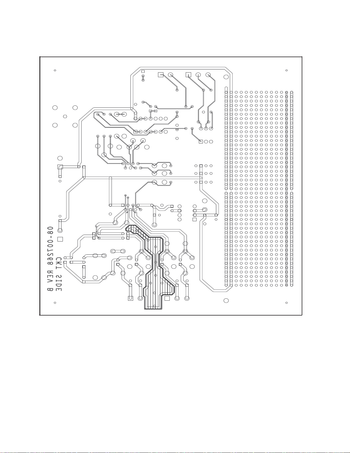
Figure 10. PCB Layout–Solder Side
–10–
REV. PrF
PRELIMINARY TECHNICAL DA T A
EVAL-ADE7757EB
REV. PrF
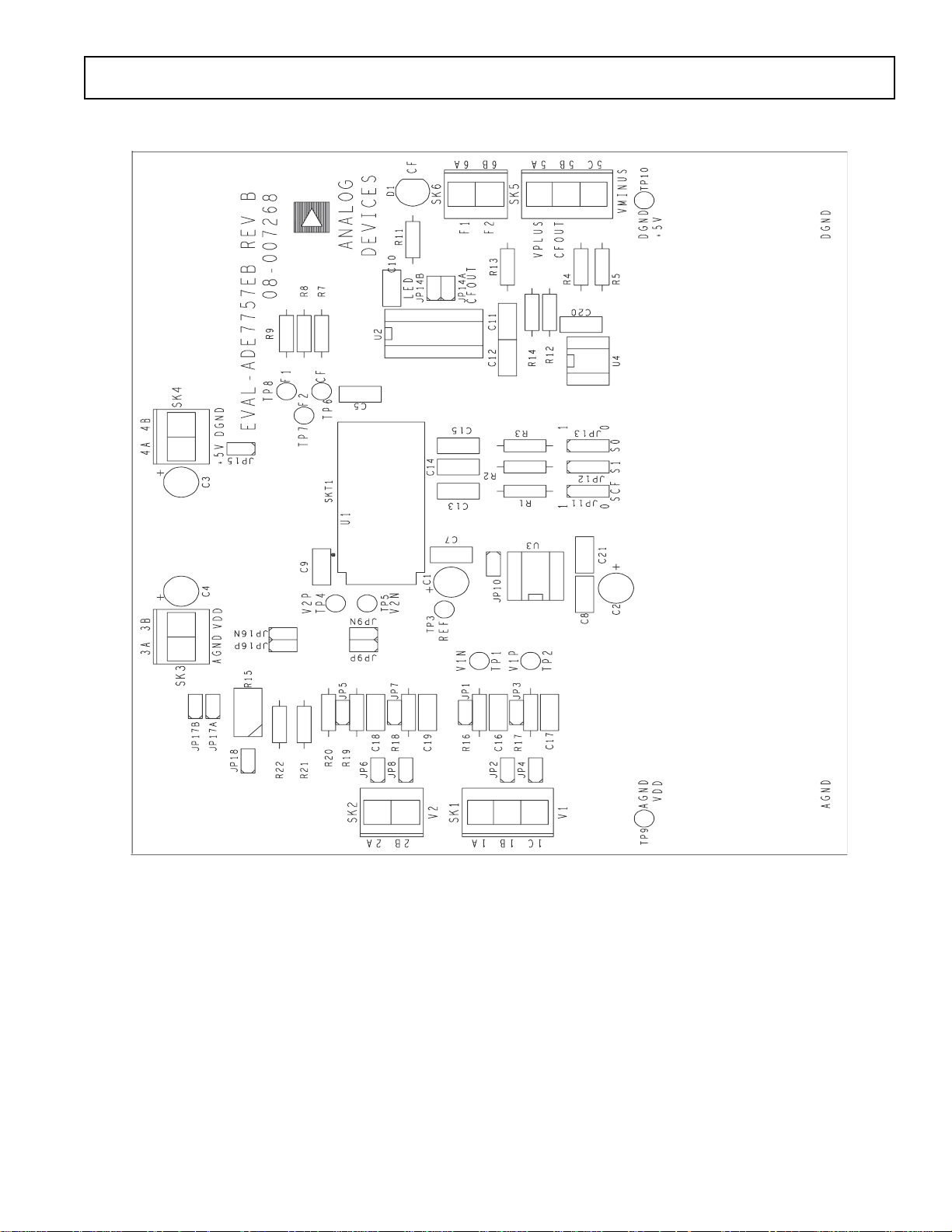
Figure 11. PCB Layout–Component Placement
–11–
 Loading...