

查询EVAL-AD974CB供应商
Evaluation Board
a
AD974 4-Channel, 16-Bit, 200 kSPS ADC
FEATURES
Versatile Analog Signal Conditioning Circuitry
Jumper Selectable Analog Input Ranges
Analog and Digital Prototyping Area
Flexible Power and Grounding Schemes
On-Board Reference and Buffers
16-Bit Serial and Parallel Buffered Outputs
Ideal For DSP and Data Acquisition Card Interfaces
EVAL-CONTROL BOARD Compatibility
PC Software for Control and Data Analysis
GENERAL DESCRIPTION
The EVAL-AD974CB is an evaluation board for the AD974
four-channel, 16-bit data-acquisition system. The AD974 is
capable of a 200 kSPS throughput rate, operates from a
single +5 V supply and uses a flexible serial interface.
The AD974 evaluation board is designed to demonstrate
the ADC’s performances and to provide an easy to understand interface for a variety of system applications. A full
description of the AD974 is available in the AD974 data
sheet and should be consulted when using this evaluation
board.
EVAL-AD974CB
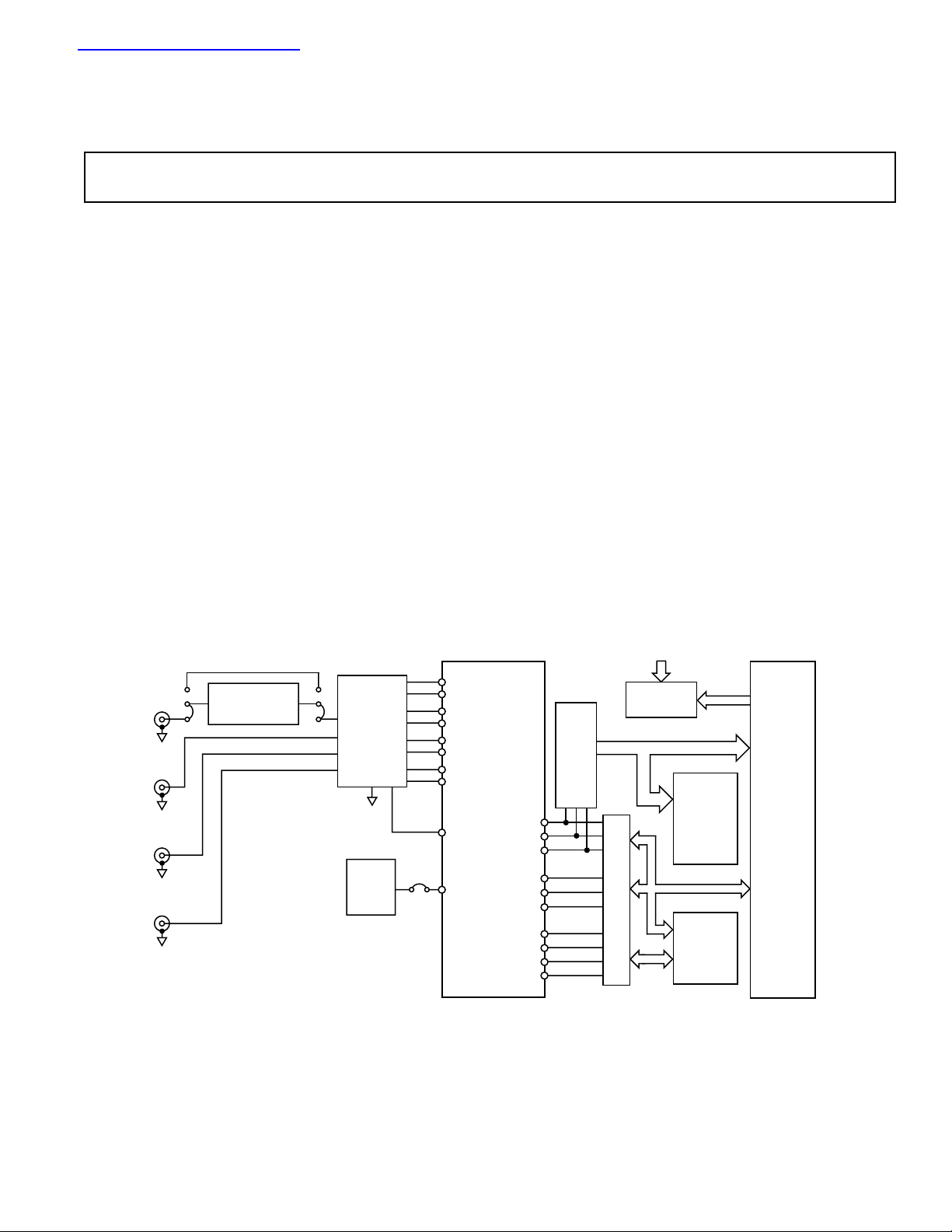
The EVAL-AD974CB is ideal for use as either a stand-alone
evaluation board to interface with customer application, or with
the EVAL-CONTROL BOARD, also available from Analog
Devices. The design offers the flexibility of applying external
control signals and is capable of generating 16-bit conversion
results as both serial and parallel buffered outputs.
On-board components include an AD780, a +2.5 V ultrahigh
precision bandgap reference, an AD845 signal conditioning op
amp, and digital buffers. The board interfaces with a 96-pin
connector for the EVAL-CONTROL BOARD, a 20-pin IDC
connector for both externally applied control signals and serial
output interfaces, and a 40-pin IDC connector for parallel
output data. SMB connectors are provided for the low noise
analog signal source and BNC connectors are provided for an
external data clock and an external read/convert input.
AIN1
AIN2
AIN3
AIN4
SIGNAL
CONDITIONING
AD845
FUNCTIONAL BLOCK DIAGRAM
SELECTABLE
INPUT
RANGE
VA
VB
VA
VB
VA
VB
VA
VB
EXT/INT
1
1
2
2
3
3
4
4
PWRD
AD974
DATA
DATACLK
BUSY
R/C
A0
A1
WR2
WR1
SYNC
CS
REF 2.5V
AD780
BIP
REF
DATA
SHIFT
REG
SELECTABLE
SUPPLY
B
U
F
F
E
R
S
40-PIN
CONNECTOR
20-PIN
CONNECTOR
ⴞ5V
ⴞ12V
V
CC
96-PIN
CONNECTOR
REV. A
Information furnished by Analog Devices is believed to be accurate and
reliable. However, no responsibility is assumed by Analog Devices for its
use, nor for any infringements of patents or other rights of third parties
which may result from its use. No license is granted by implication or
otherwise under any patent or patent rights of Analog Devices.
One Technology Way, P.O. Box 9106, Norwood, MA 02062-9106, U.S.A.
Tel: 781/329-4700 World Wide Web Site: http://www.analog.com
Fax: 781/326-8703 © Analog Devices, Inc., 2000
EVAL-AD974CB
OPERATING THE EVAL-AD974CB
The AD974-CB is a four-layer board carefully laid out and tested
to demonstrate the specific high accuracy performance of the
device. Figure 2 shows the schematics of the evaluation board.
Figure 3 shows the component side silkscreen. The layouts of
the board are given in:
Component Layer – Figure 4
Power Layer – Figure 5
Ground Layer – Figure 6
Circuit Side Layer – Figure 7.
The AD974-CB is a flexible design that enables the user to
choose among many different board configurations. The available test points are listed in Table IV and a description of each
selectable jumper is listed in Table V.
The evaluation board schematic shows the factory installed
jumper selections. The AD974 is configured for ±10 V input
range on each channel, powered through the EVAL-CONTROL
BOARD, the AD780 external reference applied to the REF pin
and on-board R/C generation used. The serial interface is configured to operate with its internal data clock, DCLK. Conversion data is available at the outputs of two 8-bit shift registers,
U4 and U5, for parallel transfer via the 40-pin IDC connector,
J4, or the 96-pin DIN connector, P5. Additionally, conversion
results are available in serial format from the 20-pin connector,
P4. The AD974 conversion control inputs, R/C and CS, are
configured to provide continuous conversions with the CS
input set low and the R/C input connected to the output of
the counter, U6.
Power Supplies and Grounding
The AD974-CB power supply connectors and ground planes are
configured to provide the multiple power and grounding configurations used in most system applications.
The evaluation board ground plane is separated into two sections: a plane for the digital interface circuitry and an analog
plane for the AD974 and its analog input and external reference
circuitry. To attain high resolution performance the board was
designed to ensure that all digital ground return paths do not
cross the analog ground return paths.
The EVAL-AD974CB has three power supply blocks: a single
+5 V supply for the AD974 V
ANA
and V
power pins (P1), a
DIG
+5 V supply for the digital interface circuitry (P2), and a ±12 V
supply for the analog signal conditioning circuitry (P3). All
supplies are decoupled to ground with 10 µF tantalum and
0.1 µF ceramic capacitors. Figure 1 shows the recommended
power connection diagram.
ANALOG
POWER SUPPLIES
+15V –15VGND +5V GND +5V GND
DIGITAL
SYSTEM POWER
Analog Input Ranges
The AD974-CB provides the flexibility of operating the AD974
in each of its specified analog input ranges. Through easy to
follow jumper selections, the four channels of the AD974 can be
operated independently in the bipolar input range ±10 V, or in
all two unipolar input ranges of 0 V to +4 V, and 0 V to +5 V.
Table I through Table III list the jumper configurations for each
input range.
Table I. ⴞ10 V Analog Input Range
Jumper Designation Header Shunt Position
JP12, JP27, JP23, JP25 B
JP11, JP26, JP22, JP24 B
Table II. 0 V to +4 V Analog Input Range
Jumper Designation Header Shunt Position
JP12, JP27, JP23, JP25 A
JP11, JP26, JP22, JP24 B
Table III. 0 V to +5 V Analog Input Range
Jumper Designation Header Shunt Position
JP12, JP27, JP23, JP25 A
JP11, JP26, JP22, JP24 A
Table IV. EVAL-AD974CB Test Points
Test Point Available Signal
TP1 AIN1 (BUFFERED)
TP2 BUSY
TP3 R/C
TP4 DGND
TP5 VDIG
TP6 AGND1
TP7 SYNC
TP8 DCLK
TP9 DATA
TP10 CAP
TP11 AGND
TP12 AIN1 (SMB)
TP13 –VCC
TP14 +VCC
TP15 VANA
TP16 AGND
TP17 R/C (BNC)
+V
–V
AGND V
CC
P3 P1
P4
AGND
EE
ANA
P2
V
DGND
DIG
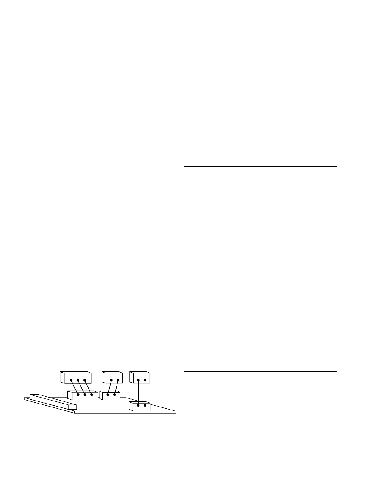
Figure 1. Power Connection Diagram
–2–
REV. A

EVAL-AD974CB
EVAL-CONTROL BOARD Interface
The EVAL-AD974CB interfaces to the EVAL-CONTROL
BOARD through the 96-pin connector.
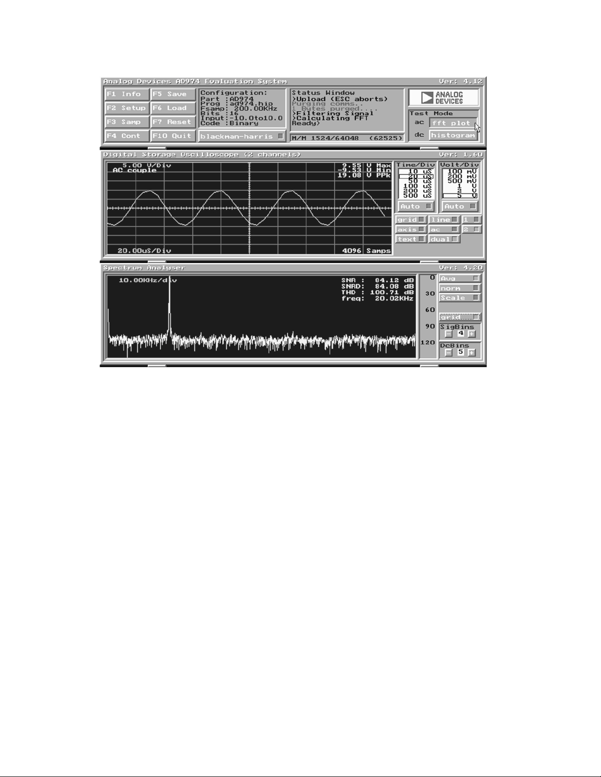
RUNNING THE EVAL-AD974CB SOFTWARE
Software Description
The EVAL-AD974CB comes with software for analyzing the
AD974. Through the EVAL-CONTROL BOARD one can
perform a histogram to determine code transition noise, and
Fast Fourier Transforms (FFT’s) to determine the Signal to
Noise Ratio (SNR), Signal to Noise plus Distortion (SNRD)
and Total Harmonic Distortion (THD). The front-end PC
software has three screens as shown in Figures 8, 9 and 10.
Figure 8 is the Setup Screen where channel selection, input
voltage range, sample rate, number of samples are selected.
Figure 9 is the Histogram Screen, which allows the code distribution for dc input and computes the mean and standard
deviation. Figure 10 is the FFT Screen, which performs an
FFT on the captured data, computes the Signal-to-Noise
Ratio (SNR), Signal to Noise plus Distortion (SNRD) and
Total Harmonic Distortion (THD).
Table V. Jumper Description
Jumper
Designation Function
JP1 JP1 controls the state of the AD974 power-down pin, PWRD. With JP1 in Position B, conversions are inhibited
and the AD974 power consumption is significantly reduced. For normal operation of the AD974, JP1 should be in
Position A.
JP2 JP2 selects the EXT/INT input to the AD974. Set JP2 to Position B and the AD974 requires an external data
clock to transmit data. Position A chooses the internal clock mode.
JP3 JP3 allows use of an external DCLK. When J2 is in Position A, internal clock mode is used and JP3 should be
removed. When J2 is in Position B, external clock mode is used and the signal EXT DCLK from BNC connector,
J2 is applied to the DCLK input of the AD974.
JP4 With JP5 set to Position A, JP4 selects the signal source for the R/C input to the AD974. Set JP4 to Position A to
use the on-board 200 kHz signal from the 74HC190. Select Position B to use the external R/C signal from the
BNC connector, J1.
JP5 With JP5 in Position A, the R/C input to the AD974 is applied from either the 74HC190 or the external source,
J1. With JP5 in Position B, the R/C input is a buffered signal (FL0) from the EVAL-CONTROL BOARD and an
input from the 20-pin IDC connector.
JP6 JP6 selects the WR2 input to the AD974. With shunt header in JP6, the AD974 WR2 input is tied to a logic low.
When shunt header in JP6 is removed, the AD974 WR2 input comes from the 20-pin IDC connector.
JP7 JP7 selects the WR1 input to the AD974. With shunt header in JP7, the AD974 WR1 input is tied to a logic low.
When shunt header in JP7 is removed, the AD974 WR1 input comes from the 20-pin IDC connector.
JP8 JP8 selects the CS input to the AD974. With shunt header in JP8, the AD974 CS input is tied to a logic low.
When shunt header in JP8 is removed, the AD974 CS input comes from the 20-pin IDC connector.
JP9 JP3 allows use of an external read clock, EXT RCLK. With shunt header in JP9, the AD974 BUSY signal enables
the data reading. When shunt header in JP9 is removed, the signal EXT RCLK from BNC connector, J5 enables
the data reading.
JP10 With JP10 set to Position A, gain adjustment for the AD974 is possible. Position B selects the AD780 for use as an
external reference. Remove the shunt header of JP10 to use the AD974 internal reference without gain adjustment.
JP11, JP12 These TWO jumpers set the analog input ranges for Channel 1 according to Table I through Table III.
JP13 With JP13 tied to Position A, the analog Channel 1 input comes from either the analog signal source (AIN1) from
J3, or the output of the op amp, U3. Set to Position B, the analog input is tied to analog ground.
Software Installation
The AD974-CB software runs under DOS 4.0 or higher. It
requires a minimum of 386-based machine, with 500 kB of base
RAM and 500 kB of free hard disk space. It may be necessary to
disable some TSRs (network TSRs for example) or load them
into high memory, to ensure that adequate base memory is available. Operation under Windows
the Windows COM interrupt can interfere with communication
between the PC and the EVAL-CONTROL BOARD. For PC
running under Windows 95, it is recommended to shut it down
using the option restart with the computer in MS-DOS mode.
The AD974-CB software installation process is:
– Create a new directory on the main PC drive and label this
“AD974.”
– Copy into this directory all files contained in the disk that
accompanies the EVAL-AD974CB.
– The software can be started by typing “AD974.”
Note that the Mouse Driver on the PC should be enabled
before running the software. If this has not been loaded,
the program will not run.
®
3.x is not recommended since
Windows is a registered trademark of the Microsoft Corporation.
–3–REV. A

EVAL-AD974CB
Jumper
Designation Function
JP14 JP14 determines the source of the analog Channel 1 input of the AD974. To supply the AD974 analog Channel 1
input signal directly from the SMB connector, J3, set JP14 to Position B. Set JP14 to Position A to select the op
amp output.
JP15, JP16 These two jumpers are used to select the configuration of the op amp, U3. To configure the op amp as an inverter,
install the header shunt of JP15 to Position A and JP16 to Position B. To configure the op amp as a noninverter,
install the header shunt of JP15 to Position B and JP16 to Position A.
JP17 JP17 selects the digital power source for the AD974-CB digital interface circuitry. Install the jumper to provide a
single +5 V supply to all of the on-board components. Remove this header shunt to separate the analog supply
for the AD974 from the supply for the digital interface circuitry. When used in conjunction with the EVALCONTROL BOARD, V
header shunt is installed, JP28 must also be installed.
JP18 With JP19 in Position B, the header shunt for JP18 allows the positive supply voltage of op amp, U3, to come
from either connector P3 (Position A), or the +12 V supply from the EVAL-CONTROL BOARD (Position B).
JP19 With JP19 set to Position A, the positive supply for the op amp, U3, is connected to VANA. When JP19 is set to
Position B, U3’s positive supply voltage is connected to either the +12 V from the EVAL-CONTROL BOARD
(JP18 Position B), or the external supply (+V
JP20 With JP21 in Position A, the header shunt for JP20 allows the negative supply voltage of op amp, U3, to come
from either connector P3 (Position B), or the –12 V supply from the EVAL-CONTROL BOARD (Position A).
JP21 With JP21 set to Position B, the negative supply for the op amp, U3, is connected to analog ground (AGND).
When JP21 is set to Position A, U3’s negative supply voltage comes from either the –12 V from the EVAL-CON-
TROL BOARD (JP20 Position A) or the external supply (–V
JP22, JP23 These TWO jumpers set the analog input ranges for Channel 3 according to Tables I through Table III.
JP24, JP25 These TWO jumpers set the analog input ranges for Channel 4 according to Tables I through Table III.
JP26, JP27 These TWO jumpers set the analog input ranges for Channel 2 according to Tables I through Table III.
JP28 Install JP28 when using a single +5 V supply for the EVAL-CONTROL BOARD. Thus, install JP28 when JP17 is
connected.
ANA
and V
are respectively the +5 V and VDD from the 96-pin connector. When this
DIG
) from connector P3 (JP18 Position A).
CC
) from connector P3 (JP20 Position B).
CC
–4–
REV. A

EVAL-AD974CB
CS (C-10)
D15 (C-19)
D14 (C-18)
D13 (B-18)
12
D15
D14
D13
NC
9
7
65432115
QH
QH
QG
74HC595
CC
V
GND
1681312101114
DIG
V
C18
0.1F
–12V
+12V
CC
–V
CC AGND
+V
A
JP20
P3
B
A
JP18
B
ANA
V
P2
DGND
DIG
V
DD
V
DIG
V
TP5TP15
JP28
ANA
V
+5V
P1
ANA
V
AGND
D12 (A-18)
D11 (B-17)
D10 (B-15)
D12
D11
QF
QE
QDQCQB
U4
RCLK
G
B
JP21
A
TP13
B
TP14
JP19
A
TP4
C15
0.1F
C14
10F
JP17
C13
10F
C12
0.1F
TP16
D9 (B-14)
D8 (B-13)
D7 (B-11)
D6 (B-10)
D5 (B-9)
D4 (B-7)
D3 (B-6)
D2 (B-5)
D1 (B-3)
D0 (B-2)
D9D8D7D6D5D4D3D2D1
D10
9
QA
74HC595
SRCLK
SRCLR
SER
DIG
V
R9
49.9k⍀
CC
–V
C16
0.1F
1,8,12,14,15
74HC366
16
DIG
V
DIG
CC
V
+V
DIG
V
U7
C21
0.1F
1,10,19
20
U8
TP1
B
CC
+V
C11
R3
2k⍀
C10
2nF
C17
JP15
TP12
AIN1
AVDD (A,B,C-32)
+5V
+12V (C-30)
AVSS (A,B,C-31)
–5V
+12V
–12V
D0
BUSY
7
65432115
QF
QE
QH
QH
QG
QDQCQB
U5
CC
V
GND
RCLK
G
SRCLR
1681312101114
C19
0.1F
C22
0.1F
1,4–10,19
74HC541
20
U9
B
A
JP11
74HC541
JP12
A
B
B
A
A
JP13
JP14
CC
–V
C8
10F
10F
0.1F
C9
U3
AD845
R1
R2
1k⍀
B
A
J3
0.1F
499⍀
B
A
JP16
J8
AIN2
–12V (A-30)
DD
V
QA
SRCLK
SER
B
JP27
JP26
A
AIN3
(A,B,C-8)
CC
V
39 40
40-PIN IDC
CONNECTOR
J4
U7
U7 U7 U7
23456789
28
2726252423
VB2
VA2
AGND1
VA3
1
2
TP6
B
JP23
JP22
A
A
B
J6
IRQ2 (C-17)
BUSY
VB1
VB3
A
B
JP25
AIN4
3
ANA
V
B
A
VA1
VA4
4
A
JP24
J7
FL1 (B-1)
A0
C7
0.1F
V
VB4
5
B
FL0 (A-17)
R/C
3
U8
17
4
U8
16
A0
ANA
BIP
6
ANA
V
RFS0 (C-6)
DATA
BUSY
12
U8
8
TP2
22
A1
U1
AD974
CAP
7
TP10
C6
A
R4
576k⍀
VR2
50k⍀
DR0 (C-5)
SCLK0 (A,C-7)
DCLK
11
U8
9
JP9
21
20
CS
BUSY
REF
AGND2
9
8
2.2F
C4
B
JP10
SCLK1 (A,C-3)
F0 (A-1)
A1
15
5
6
U8
14
TP9
1918171615
WR1
WR2
DATA
DIG
R/C
V
PWRD
1011121314
TP3
C5
0.1F
ANA
V
2.2F
C1
876
O/P
NC
OUT
V
5
TRIM
SELECT
IN
+V
NC
TEMP
GND
4
3
2
1
C2
ANA
V
C3
1F
DGND
(A,B,C-4,12,16,20)
U8
TP8
17
U9
3
DCLK
SYNC
EXT/INT
DGND
TP11
VR1
50k⍀
330F
R5
U2
AD780
0.1F
AGND
(A,B,C-21,22,23,24,
25,26,29 B-27,28,30)
JP8
JP6
18
JP3
TP7
13
18
B
JP5
JP4
A
A
C21
0.1F
ANA
+V
V
1M⍀
OUT
C20
0.1F
ANA
V
16151413121110
A
CC
V
CLK
BQBQA
3
2
1
P5
96-PIN DIN
CONNECTOR
JP7
2
U9
DIG
V
7
U8
DIG
V
2
U8
B
GND
ANA
V
RCO
CTEN
4
P4
20-PIN IDC CONNECTOR
1
2
20
19
J5
J2
EXT DCLK EXT RCLK
R8
49.9⍀
B
JP2
A
R10
49.9k⍀
B
JP1
A
R7
49.9k⍀
J1
R/C
R6
TP17
49.9⍀
X1
2.000MHz
98
C
D
LOAD
MX/MN
D/UQCQD
5
U6
GND
7
6
74HC190
Figure 2. Schematic
–5–REV. A

EVAL-AD974CB
Figure 3. Component Side Silkscreen (Not to Scale)
Figure 4. Component Side (Not to Scale)
Figure 5. Ground Layer (Not to Scale)
Figure 6. Power Layer (Not to Scale)
Figure 7. Circuit Side (Not to Scale)
–6–
REV. A

EVAL-AD974CB
Figure 8. Setup Screen
Figure 9. Histogram Screen
–7–REV. A
EVAL-AD974CB
C00910–0–7/00 (rev. A)
Figure 10. FFT Screen
PRINTED IN U.S.A.
–8–
REV. A
 Loading...