

查询EVAL-AD7650CB供应商查询EVAL-AD7650CB供应商
PRELIMINAR Y TECHNICAL DATA
=
Preliminary Technical Data
FEATURES
Versatile Analog Signal Conditioning Circuitry
On-Board Reference, Crystal Oscillator and Buffers
16-Bit Parallel Buffered Outputs
Ideal For DSP and Data Acquisition Card Interfaces
Analog and Digital Prototyping Area
EVAL-CONTROL BOARD Compatibility
PC Software for Control and Data Analysis
GENERAL DESCRIPTION
The EVAL-AD766XCB/AD767XCB is an evaluation board
for the AD766X/AD767X 16-bit A/D converter family. The
AD766X/AD767X family ( see ordering guide for product list )
is a high speed, successive approximation based architecture
with very high performance, low power family of 16-Bit ADCs
which operate from a single +5V supply with a 100kSPS to
1MSPS throughput rate range, and a flexible parallel or serial
interface. The AD766X/AD767X evaluation board is designed
to demonstrate the ADC's performance and to provide an easy
to understand interface for a variety of system applications. A
full description of the AD766X/AD767X is available in the
Analog Devices AD766X/AD767X data sheets and should be
consulted when utilizing this evaluation board.
Evaluation Board AD766X/AD767X
EV AL-AD766XCB/AD767XCB
The EVAL-AD766XCB/AD767XCB is ideal for use with
either the Analog Devices EVAL-CONTROL BOARD, or as a
stand-alone evaluation board. The design offers the flexibility
of applying external control signals and is capable of generating
16-bit conversion results on a parallel buffered outputs.
On-board components include an AD780, a +2.5V ultrahigh
precision bandgap reference, a signal conditioning circuit
with two op-amps and digital logic. The board interfaces with
a 96-way connector for the EVAL-CONTROL BOARD, a
20-pin IDC connector for serial output interface, and a 40pin IDC connector for parallel output data. SMB connectors
are provided for the low noise analog signal source, an external master clock and an external start/convert input.
ORDERING GUIDE
Evaluation board Model Product
EVAL-AD7650CB AD7650AST
EVAL-AD7660CB AD7660AST
EVAL-AD7662CB AD7662YST
EVAL-AD7663CB AD7663AST
EVAL-AD7664CB AD7664AST
EVAL-AD7665CB AD7665AST
EVAL-AD7668CB AD7668YST
EVAL-AD7671CB AD7671AST
EVAL-AD7675CB AD7675AST
EVAL-AD7676CB AD7676AST
EVAL-AD7677CB AD7677AST
EVAL-CONTROL BRD2 Controller Board
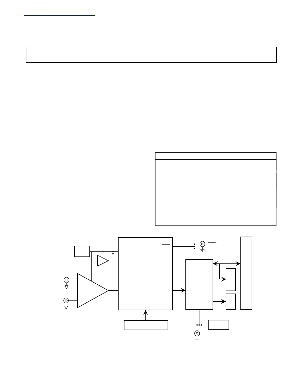
FUNCTIONAL BLOCK DIAGRAM
REF 2.5V
AD780
REF
AD766x
or
AUX_IN
SIGNAL
CONDITIONING
IN
REV. PrK
Information furnished by Analog Devices is believed to be accurate and
reliable. However, no responsibility is assumed by Analog Devices for its
use, nor for any infringements of patents or other rights of third parties
which may result from its use. No license is granted by implication or
otherwise under any patent or patent rights of Analog Devices.
AD767x
IN
Configuration switches
+/-5 V
+/-12 V
+5 V
V
L
96
PIN
CONN
MCLK
CNVST
Clock
40
PIN
CONN
20
PIN
CONN
CNVST
BUSY
DIGITAL LOGIC
DATA
MCLK
One Technology Way, P.O. Box 9106, Norwood, MA 02062-9106, U.S.A.
Tel: 781/329-4700 www.analog.com
Fax: 781/326-8703 © Analog Devices, Inc., 2001

PRELIMINARY TECHNICAL DATA
EVAL-AD766XCB/AD767XCB
OPERATING THE EVAL-AD766XCB/AD767XCB
The EVAL-AD766XCB/AD767XCB is a four-layer board
carefully laid out and tested to demonstrate the specific high
accuracy performance of the AD766X/AD767X. Figure 1
shows the schematics of the evaluation board. The layouts of
the board are given in :
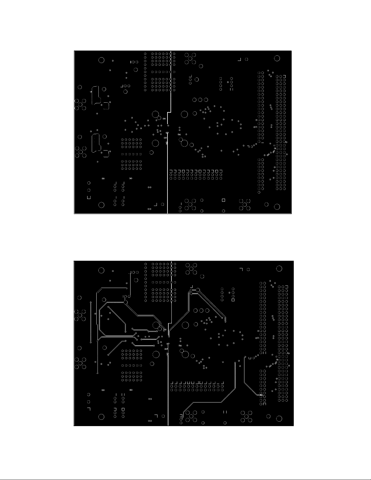
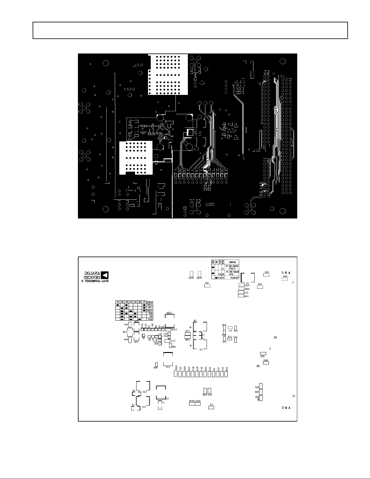
Top side silk-screen - Figure 2
Top side layer - Figure 3
Ground layer - Figure 4
Shield layer - Figure 5
Bottom side layer - Figure 6
Bottom side silk-screen - Figure 7.
The EVAL-AD766XCB/AD767XCB is a flexible design that
enables the user to choose among many different board configurations. A description of each selectable jumper/switch is
listed in Table II and the available test points are listed in
Table III. Note that the button of a switch in position A ( U3
side ) defines a low level.
The EVAL-AD766XCB/AD767XCB is configured in factory
with 0 to 2.5 V ADC input range for the AD7660, AD7664,
and AD7675/7676/7677 and +/-5V for the AD7663/7665/
7671; front-end amplifiers U6 and U7 set with a gain of +1,
powered through the EVAL-CONTROL BOARD, and the
on-board CNVST generation used.
On-board or external CNVST could be used. When an external CNVST signal is applied, this signal should have very low
jitter and sharp edges to get the best noise performance of the
part. Meanwhile, it is recommended to use the on-board
CNVST generation which is done by dividing MCLK signal
(20MHZ) by the numbers shown in Table I, which are entered in the software. Activity on BUSY pin of the ADC
turns on the LED.
Table I. CNVST GENERATION
Part Division Factor Throughput Rate
AD7660 200 100KSPS
AD7662/68 40 500KSPS
AD7663 80 250KSPS
AD7664/50 35 571KSPS
AD7665 35 571KSPS
AD7671 20 1MSPS
AD7675 200 100KSPS
AD7676 35 571KSPS
AD7677 20 1MSPS
Conversion data is available at the output bus BD on U3, on
the 40-pin connector P2, and on the 96-pin connector P3.
Additionally, BD data is updated on the falling/rising edge of
DBUSY and BBUSY on P3, low when BD data is valid are
delayed from the BD data by about 20 ns to ease the interface. When either parallel or serial reading mode of the ADC
is used, the data is available on this parallel bus. When serial
reading mode of the ADC is used, the serial interface signals
of the ADC are buffered and available on the 20-pin connec-
tor P1. When slave serial reading mode of the
AD766X/AD767X is used, the external serial clock SCLK
applied to the ADC is at half the MCLK frequency.
Power Supplies and Grounding
The evaluation board ground plane is separated into two
sections: a plane for the digital interface circuitry and an analog plane for the analog input and external reference
circuitry. To attain high resolution performance, the board
was designed to ensure that all digital ground return paths do
not cross the analog ground return paths.
The EVAL-AD766XCB/AD767XCB has three power supply
blocks: a single 5V supply VA
and the reference voltage circuitry, a digital 5V supply VL
for the digital interface circuitry and the digital section of the
ADC, and a selectable +/-12V (with a possibility of +/-15V
with control Brd2) or +/-5V supply for the analog signal conditioning circuitry (SJ3). All supplies are decoupled to ground
with 10 F tantalum and 0.1 F ceramic capacitors.
Analog Input Ranges
The analog front-end amplifier circuitry U6 and U7 allows
flexible configuration changes such as positive or negative
gain, input range scaling, filtering, addition of a DC component, use of different op-amp and supplies.
Figure 1 shows the front end op-amp configuration used with
the AD7660/7663/7664/7665/7671/7675/7676/7677.
In some applications, it is desired to use a bipolar or wider
analog input range like, for instance, ± 10V, ± 5V, ± 2.5V, or
0 to +5V. For the AD76XX parts which do not have directly
those input ranges like the AD7660/7664/7675/7676/7677,
by simple modifications of the input driver circuitry of the
EVAL-AD766XCB/AD767XCB, bipolar and wider input
ranges can be used without any performance degradation.
Components values required and resulting full-scale ranges
are shown in table IV and table V.
In factory, the analog input of U6 is set at mid-scale
(R6=R7=590⍀) for the AD7660/7664/7675/7676/7677. For
AD7663/7665/7671, R7 is not connected to maintain the
input at 0V (mid-scale). This allows a transition noise test
without any other equipment. An FFT test can be done by
applying a very low distortion AC source.
EVAL-CONTROL BOARD INTERFACE
The EVAL-AD766XCB/AD767XCB interfaces to the EVALCONTROL BRD2 through the 96-way connector.
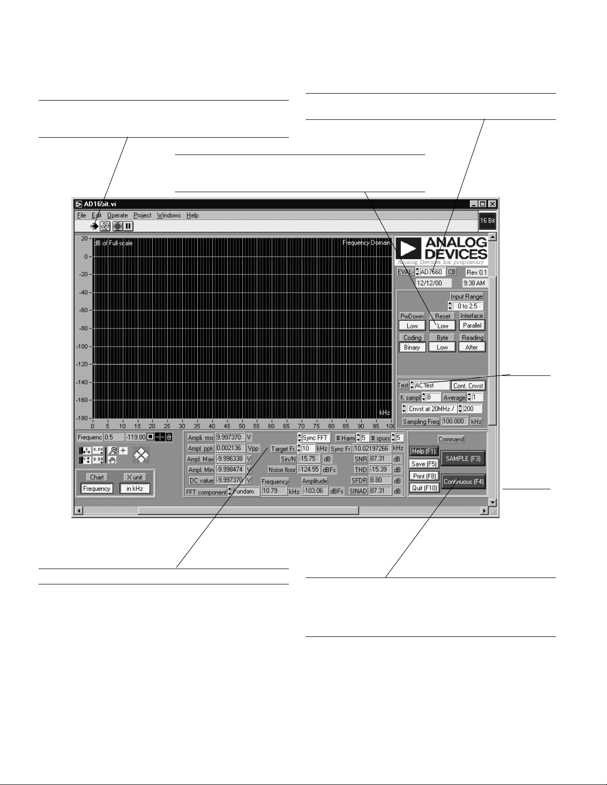
RUNNING THE EVAL-AD766X/AD767XCB SOFTWARE
Software Description
The EVAL-AD766XCB/AD767XCB comes with software for
analyzing the AD766X/AD767X. Through the EVAL-CONTROL BRD2 one can perform a histogram to determine code
transition noise, and Fast Fourier Transforms (FFT's) to
determine the Signal-to-Noise Ratio (SNR), Signal-to-Noiseplus-Distortion (SNRD) and Total-Harmonic-Distortion
(THD). The front-end PC software has four screens as
shown in Figure 8,9,10 and 11. Figure 8 is the Setup Screen
where input voltage range, sample rate, number of samples
are selected. Figure 9 is the Histogram Screen, which allows
the code distribution for DC input and computes the mean
and standard deviation.
–2–
(SJ1) for the AD766X/AD767X
REV. PrK
(SJ2)

PRELIMINARY TECHNICAL DATA
EVAL-AD766XCB/AD767XCB
Figure 10 is the FFT Screen, which performs an FFT on the
captured data, computes the Signal-to-Noise Ratio (SNR),
Signal-to-Noise-plus-Distortion (SINAD) and total-Harmonic-Distortion (THD). Figure 11 is the time domain
representation of the output. When the on-board CNVST
generation is used, a synchronous FFT could be achieved by
synchronizing the external AC generator with the Fsync signal
(TP11) which is an exact division by 2 of MCLK.
TABLE II. JUMPER DESCRIPTION
Jumper Default position Function
Designation with the control
board ( Factory
settings)
JP1 A Selection of the positive supply of the front-end amplifier U6. When JP1 is in posi-
tion A, the +12V supply from the control board is applied to JP3 otherwise VS+ on
SJ3 is used.
Software Installation
- Double-Click on Setup.exe from the CD-ROM and follow the
installation instructions.
NOTE: The software runs under Windows 95/98 only.
JP2 A Selection of the negative supply of the front-end amplifier U6. When JP2 is in posi-
tion A, the -12V supply from the control board is applied to JP4 otherwise VS- on
SJ3 is used.
JP3 A Selection of the positive supply of the front-end amplifier U6. When JP3 is in posi-
tion A, the +5V supply from the control board is used otherwise JP1 output is used.
JP4 A Selection of the negative supply of the front-end amplifier U6. When JP4 is in posi-
tion A, the -5V supply from the control board is used otherwise JP2 output is used.
JP5 not A Selection of the master clock MCLK signal. When JP5 is in position A, the signal on
J4 is used otherwise the on-board 20 MHz clock is used as a MCLK signal. MCLK
signal is used to generate the on-board CNVST signal and the external serial clock
SCLK.
JP6 A, U3 side Selection of RDC ( Read during convert ). When the button of the switch is close to
J4 connector ( not A position ) and when the serial reading mode is selected, the data
are read during conversion otherwise the data are read after conversion. JP6 has no
use in parallel reading mode.
JP7 A, U3 side Selection of PD ( Powerdown ). When the button of the switch is close to J4 connec-
tor ( not A position ), the ADC is in power-down mode.
JP8 A, U3 side Spare switch.
JP9 A, U3 side Selection of RESET. When the button of the switch is close to J4 connector ( not A
position ), the ADC is reset.
JP10 A, U3 side Selection of SER/PAR ( serial/parallel reading mode ). When the button of the switch
is close to J4 connector ( not A position ), the data are read in serial mode otherwise
the data are read in parallel mode.
JP11 not A, SJ4 side Selection of OC/2C ( coding ). When the button of the switch is close to J4 connector
( not A position ), the ADC uses a straight binary coding otherwise the twos complement coding is used.
JP12 A, U3 side Selection of WARP. When the button of the switch is close to J4 connector ( not A
position ), the ADC uses the WARP mode which is the fastest one. With the AD7660,
JP12 is a spare switch.
REV PrK
–3–

PRELIMINARY TECHNICAL DATA
EVAL-AD766XCB/AD767XCB
TABLE II. JUMPER DESCRIPTION
Jumper Default position Function
Designation with the control
board ( Factory
settings)
JP13 A, U3 side Selection of IMPULSE. When the button of the switch is close to J4 connector
( not A position ), the ADC uses the IMPULSE mode which is the mode with the
lowest power dissipation. With the AD7660, JP13 is a spare switch.
JP14 A, U3 side TEST1. For factory use only and it is pull down.
JP15 A, U3 side TEST0. For factory use only and it is pull down.
JP16 A, U3 side Selection of EXT/INT ( use of external or internal serial clock ). When the button of
the switch is close to J4 connector ( not A position ) and when the serial reading
mode is selected, the data are read with an external serial clock SCLK generated from
the master clock MCLK otherwise the data are read with the ADC serial clock. When
external serial clock reading mode is selected, MCLK has to be fast enough to be able
the read the data properly as explained in the AD766X data sheet. JP16 has no use in
parallel reading mode.
JP17 A, U3 side Selection of INVSYNC ( SYNC active level ). When the button of the switch is close
to J4 connector ( not A position ) and when the master serial reading mode is se
lected, the SYNC signal is active Low. JP17 has no use in parallel reading mode or
slave serial reading mode.
JP18 A, U3 side Selection of INVSCLK ( SCLK active edge ). When the button of the switch is close
to J4 connector ( not A position ) and when the serial reading mode is selected,
INVSCLK is high. JP18 has no use in parallel reading mode.
JP19 not A Selection of CNVST signal. When JP19 is in position A, the signal on J3 is used
otherwise the on-board CNVST generation is used. MCLK signal is used to generate
the on-board CNVST signal.
JP20 not A Selection of REF signal. When JP20 is in position A, the REF is buffered. When
JP20 is not in position A, the REF is not buffered.
Table III. EVAL-AD766XCB/AD767XCB Test Points
Test Point Available Signal
TP1 DGND Digital ground
TP2 DGND Digital ground
TP3 SIG+ ADC Analog input
TP4 AGND Analog ground close to SIG+
TP 5 REF ADC Reference input
TP6 BUSY ADC BUSY signal
TP7 RD ADC RD signal
TP8 CS ADC CS signal
TP9 AGND Analog ground close to REF
TP10 CNVST ADC CNVST signal
TP11 F
TP12 OVDD ADC digital output supply
TP13 DVDD ADC digital core supply
TP14 VANA1 ADC analog supply
TP15 AGND Analog ground close to SIGTP16 SI G- ADC Analog input
SYNC
MCLK divided by 2
Table IV. Component values Vs. Input ranges ( AD7660 )
Input range R1 R3 R6 R7
± 10V 8k⍀ 1k⍀ 8k⍀ 10k⍀
± 5V 8k⍀ 2k⍀ 6.67k⍀ 10k⍀
0 to -5V 8k⍀ 8k⍀ 0⍀ none
Table V. Component values Vs. Input ranges ( AD7664 )
Input range R1 R3 R6 R7
± 10V 2k⍀ 250⍀ 8k⍀ 10k⍀
± 5V 2k⍀ 500⍀ 6.67k⍀ 10k⍀
0 to -5V 1k⍀ 1k⍀ 0⍀ none
–4–
REV. PrK

PRELIMINARY TECHNICAL DATA
EVAL-AD766XCB/AD767XCB
TESTING METHODS
Histogram
To perform a histogram test, apply a DC signal to the input. It
is advised to filter the signal to make the DC Source noise compatible with that of the ADC. C26 provides this filtering.
AC Testing
To perform an AC test, apply a sinusoidal signal to the
evaluation board. Low distortion, better than 100dB, is required
to allow true evaluation of the part. One possibility is to filter the
input signal from the AC source. There is no suggested
bandpass filter but consideration should be taken in the choice.
Furthermore, when the full-scale input range is more than a few
Vpp, it is recommended that you use the on board amplifier to
amplify the signal, thus preventing the filter from distorting the
input signal.
Please refer to Figures 8,9,10 and 11 to see the screens of the
software.
Software Description
The AD16bit.exe is the software which allows you to analyze
different performance characteristics of the AD766X,
AD767X, AD97X and AD67X 16-bit ADC family. The software allows you to test the histogram as well as perform
different AC tests.
Setup Requirements
- Evaluation Control Board 2 (ADSP2189)
- Evaluation Board
- Power Supply (AC 15V/1A source could be bought from
ADI)
- Parallel Port Cable (provided with the evaluation control
board)
- AC Source (low distortion)
- DC Source (low noise)
- Bandpass Filter (value based on your signal frequency, low
distortion)
USE OF EVAL-AD766XCB/AD767XCB AS STANDALONE EVALUATION BOARD
You have the option of using the
EVAL-AD766XCB/AD767XCB as a stand-alone evaluation
board. This method does not require the control board, nor does
it require use of the accompanied software. The digital output
will now be available on P1 (20-pin connector, for use in serial
mode) or P2 (40-pin connector, for use in parallel mode). Certain modifications have to be made on the board to allow proper
operation of the evaluation board. Refer to Table II to obtain
the jumper positions for stand-alone operation. When in standalone, CNVST could be externally applied or is generated
internally according to Table I.
Please refer to Figure 1 to obtain the data output pins on the
connectors.
Data is updated on the falling edge of BUSY. BCS and BWR
are inputs to the FPGA and are connected to P1 and P2.
When BCS, CONTROL are low and BWR is high, which is
the default value defined by the on-board pull-up/pull-down
resistors, the data bus BD available on the P2 connector is
enabled.
SUPPLYING THE BOARD FOR STAND-ALONE USE
SJ1 is the analog supply. Connect VA+ to +5V and AGND to
GND. SJ2 is the digital supply. SJ2 requires the same values as
SJ1, and SJ2 may be connected to SJ1. SJ3 is the supply for the
front end amplifier (U6). Connect +12V to VS+, GND to
AGND, and -12V to VS-.
REV PrK
–5–

PRELIMINARY TECHNICAL DATA
EVAL-AD766XCB/AD767XCB
EVAL-BOARD SETTING FOR INPUT
CONFIGURATIONS
The AD7663/AD7665 and AD7671 have the ability to operate both unipolar and bipolar range. The available options are
+/- 10V, +/- 5V, +/- 2.5V, 0 to 10V, 0 to 5V and 0 to 2.5V.
Table VI shows the required configurations for each input
range. (REF = 2.5V). Table VII lists the default settings of
the board for all parts.
Table VI. AD7663/7665/7671 Analog Input Configuration
Input Voltage IND(4R) INC(4R) INB(2R) INA(R)
Range
±4 REF V
±2 REF V
±REF V
0 V to 4REF V
0 V to 2REF V
0 V to REF V
IN
IN
IN
IN
IN
IN
INGND INGND REF
V
IN
V
IN
V
IN
V
IN
V
IN
INGND REF
V
IN
INGND INGND
V
IN
V
IN
REF
INGND
V
IN
Table VII. Default Settings
Component/Part R7 S9 S10 R48 C40 R47 C39
AD7660 590⍀ None 0⍀ 0⍀ None
AD7663 None None 0⍀ 0⍀ None
AD7664 590⍀ None 0⍀ 15⍀ 2.7nF
AD7665 None None 0⍀ 0⍀ None
AD7671 None None 0⍀ 0⍀ None
AD7675 590⍀ 0⍀ None 15⍀ 2.7nF 15⍀ 2.7nF
AD7676 590⍀ 0⍀ None 15⍀ 2.7nF 15⍀ 2.7nF
AD7677 590⍀ 0⍀ None 15⍀ 2.7nF 15⍀ 2.7nF
–6–
REV PrK

PRELIMINARY TECHNICAL DATA
EVAL-AD766XCB/AD767XCB
D[0..15]
VANA2
V+
C10
10uF
TP14
VANA
C9T
R34
0.0
VANA2
C1
.1uf
TP13
DVDD
OVDD
GND
TP12
VANA
DVDD
C9B
.1uF
OVDD
R67
0.0
1
S19
S18
U2A
1
-2+
4 8
GND
3
R66
GND
5
6
+
AD8032AR
U2B
7
SIG_2.5V
C33
10uF
GND
C25
.1uF
GND
VOUT
GND
U5
1uF
2
AD780BR
C30
8
6
VOUT
2.5/3vSEL
+VIN
7
GND
C27
VANA2
VANA2
D[0..15]
GND
D0
D1
D2
D4
D5
D6
D7D8D9
D10
D11
15
14
D4/EXT/INT
D6/INVSCLK
D5/INVSYNC
22
16
21
D8/SDOUT
D7/RDC/SDIN
38
23
D9/SCLK
D10/SYNC
REFGND
24
D11/RDERROR
12
11
13
9
U1
DGND
17
D110D0
DGND
20
AGND
1
2
19
18
AVDD
DVDD
OVDD
REF
TP5
D3/DIVSCLK(1)
D2/DIVSCLK(0)
REF
37
C32B
47uF
C31B
A
1uF
REF
C31T
JP20
AGND
TP9
GND
C5
10uF
GND
VR1
50K
TP3
R8
1 Meg
C20
C29
.1uF
.1uF
.1uF
V+
5
TRIM
GND
4
GND
TEMP
N/C1N/C
3
C28
.1uF
SIG+
GND
U6
7
S16
R3
C19
0.0
R2
GND
D12
D13
D1225D1326D1427D15
S13
S12
8
2
R1
J1
AIN+
D14
D15
28
SIG_2.5V
SIG+
6
3
R5
CNVST
35
CNVST
AD766X
IN_D
S11
R48
R46
5
AD8021
4
1
0.0
BUSY
RD
A0
29
31
3
A0
RD
BUSY
IN_A40IN_B/INA141IN_C/REFA42IN_D/IN+43INGND/IN-39INB146T047INB244INBN45T1
IN_A
IN_B
IN_C
S14
S15
S6
S4
S1 S2
15
0.0
C34
10pF
C22
.1uF
V-
R70
C26
R6
590
R7
590
GND
CS
32
CS
INGND
AD766X Evaluation Board
T0
T1
PD
BYTE
WARPD3OB/2C
RESET
SER/PAR
T0/EOC
IMPULSE
INB1
INB2
INBN
T0/E0C
T1/PDREF
SER/PAR
OB/2C
WARP
IMPULSE
RESET
BYTESWAP
PD
48
T1/PDREF
36
30
8
5
6
7
33
4
34
C13
GND
B
Date:
Date:
M.M
A.G
D
23
Drawn By:
Appr. By:
Rev# Size
Sheet of
Printing Date: 4-Oct-2001
S9
S10
S8
S20
GND
S7
S3 S5
C40
C39
R47
15
C38
0.0
R45
TP16
SIG-
SIG-
C35
10pF
GND
C42
.1uF
V-
R71
C41
R29
590
R60
590
SIG_2.5V
GND
SIG_2.5V
C37
.1uF
GND
U7
V+
R44
S17
V+
7
C36
R42
0.0
R43
GND
V-
5
6
AD8021
4
1
8
2
3
R59
R61
0.0
J2
AIN-
GND
Figure 1. Schematic
REV PrK
TP4
AGND
–7–
TP15
AGND

PRELIMINARY TECHNICAL DATA
EVAL-AD766XCB/AD767XCB
R10
10K
R40
10K
DATA DCL K
R32
10K
R62
1K
R58
1K
R23
1K
EPC1441
U8
C7
.1uF
C18
.1uF
VDIG
C17
.1uF
C16
.1uF
C15
.1uF
C12
.1uF
C11
.1uF
R31
VDIG
CNVOUT
BWR
CONFIG
CONF_DONE
CS4OE
DATA1DCLK
DATA
GND
86
DATA
U3
27
D0D1D2D3D4D5D6
D[0..15]
D[0..15]
TP10
&1967
1 Meg
JP19
STATUS
3
2
DCLK
89
DCLK
D324D225D126D0
17
CNVST
CNVSTIN
P3A
C5C6C7
C19
B18
A18
B17
B15
C18
SDOUT
SYNC
SCLK
BD10
BD11
BD12
BD13
BD14
BD15
1 2
3 4
5 6
7 8
P2
BD11
BD12
BD13
BD14
BD15
BD0
BD1
BD2
BD3
BD4
AD0
AD1
78
77
82
41
BD3
AD040AD1
D811D714D615D516D4
D12
D11
D10
D13
D9
2
8
9
1
10
100
D10
D8
D9
D11
D7
D12
D13
D14
TP6
BUSY
5'
TP7
TP8
&6
R10B
100
A
R10A
100
J3
GND
B14
B13
B11
B10
BD6
BD7
BD8
BD9
9 10
11 12
13 14
15 16
BD7
BD8
BD9
BD10
BD5
BD6
BD7
BD8
BD4
EPF6010T(100)
BUSY
D1599D14
SCLKIN
98
96
13
D15
BUSY
B9
BD5
17 18
19 20
BD6
BD9
BD966BD873BD774BD675BD576BD279BD180BD0
CS95RD
CS
RD
B7B6B5B3B2
BD2
BD3
BD4
21 22
23 24
25 26
BD3
BD4
BD5
BD10
BD11
BD12
61
CNVST
BYTE
CNVSTOUT
90
32
91
BYTE
CNVST
BYTE
49.9
R41
CNVST
CNVOUT
BD1
BD2
BD13
94
RESET
BD0
27 28
BD1
BD14
51
RESET
WARP
RESET
OVDD DVDD
29 30
BD14
WARP
L2
A14
AD1
BD0
BD15
OB/2C
C15
AD0
31 32
DBUSY
83
BD1550BD1358BD1259BD1160BD10
SER/PAR
OB/2C
A32
+5V
33 34
35 36
CONTROL
84
DBUSY
CONTROL
IMPULSE29SER/PAR28OB/2C31WARP30PD
IMPULSE
SER/PAR
IMPULSE
B32
C32
A31
-5V
37 38
39 40
BCS
BWR
ADCOK
BRD
49
64
65
BWR
ADCOK
TEST0
TEST1_OUT
93
92
97
T0
PD
TEST1_OUT
T0
C8
10uF
C5B
P3B
A8B8C8
B31
C31
C30
-12V
+12V
VDIG
GND
VDIG
A9C9B1
A30
A4
C10
C17
A12
A16
A20B4B12
B16C4C12
C16
C20
A17
R24
BCS
BBUSY
BRD
BWR
DSEL
CONTROL
10K
B20
B26
B27
B28
B29
B30
C21
C22
C23
C24
C25
C26
C29
A21
A22
R26
R27
R30
R33
10K
10K
10K
357
10K
A23
A24
A25
R28
D3
SDIN
SCNVST
GND
BCS
A26
P3C
GND
A29
B21
B22
B23
B24
B25
B
3
Date:
Date: AD766x Evaluation Board
M.MD9A.G
D
A K
1 2
3 4
5 6
7 8
9 10
11 12
13 14
15 16
SDOUT
43
SDOUT
17 18
SYNC
SCLK
SDIN
MCLK
STATUS
CONF_DONE
39
35
42
72
SDIN
MCLK
STATUS
CONF_DONE
P1
DATA
DCLK
BBUSY
DSEL
SCNVST
SCLK
SYNC
44
48
63
62
46
47
BCS
BRD
DSEL
SCLK
SYNC
BBUSY
SCNVST
A0
EOC12PDREF
33
34
PD
A0
0.0
R64
R65
R63
0.0
T0/EOC
T1/PDREF
.1uF
GND
V+V-
19 20
CONFIG
36
CONFIG
V+V-
1K
J5
FSYNC
GND
22
4
CE
MSEL
ADCOK
GND
C3
.1uF
4
2
VDIG
+5v
GND
OUT
20MHz osc
U4
3
1
VDIG
J4
MCLK
JP5
A
RDC
D7
D6
D5
D4
T0
TEST1_OUT
SER/PAR
OB/2C
WARP
IMPULSE
RESET
BYTE
PD
C21
10uF
GND
C23
10uF
R35
10K
10K
10K
10K
100
10K
10K
10K
10K
INVSCLK
R22 10K
INVSYNC
R21
EXT/INT
R20
TEST0_IN
R19
T1
R18
R15
R14
R16 10K
R17
R13 10K
R12
R11 10K
VDIG
T1
D1
R36
TP2
TP1
R23B
R23A
R38
TEST1_OUT
TEST0_IN
R37
DGND
DGND
10K
10K
10K
10K
Drawn By:
JP6
JP18
JP17
JP16
JP15
JP14
JP10
JP11
JP12
JP13
JP9
JP8
JP7
Appr. By:
GND
Rev# Size
2of
Printing Date: 28-Sep-2001
.1uF
C2
10uF
GND
VANA2+5v
VANA2
L1
1
2
SJ1
VA+
AGND
GND
GND
VDIG OVDD DVDD
C5T C7T C7B
C6
10uF
L3
C4
10uF
1
2
SJ2
VL
DGND
+5V
+12V
L4
L5
A
JP3
GND
A
JP1
123
SJ3
VS-
VS+
AGND
-5V
A
JP4
-12V
A
JP2
Figure 1 Schematic
–8 –
REV. PrK

PRELIMINARY TECHNICAL DATA
EVAL-AD766XCB/AD767XCB
Figure 2. Top side silk-screen ( Not to Scale ).
Figure 3. Top side ( Not to Scale ).
REV PrK
–9–
PRELIMINARY TECHNICAL DATA
EVAL-AD766XCB/AD767XCB
Figure 4. Ground Layer ( Not to Scale ).
Figure 5. Shield Layer ( Not to Scale ).
–10–
REV. PrK
PRELIMINARY TECHNICAL DATA
EVAL-AD766XCB/AD767XCB
Figure 6. Bottom side layer ( Not to Scale ).
Figure 7. Bottom side silk-screen ( Not to Scale ).
REV PrK
–11–
PRELIMINARY TECHNICAL DATA
EVAL-AD766XCB/AD767XCB
1) The Run button starts the software. All input configurations
are read by the software after running the software. You will
need to press this button first.
3) Input Configurations are chosen here. For the AD766X/
AD767X, the available choices are: PwDown, Reset, Interface,
Coding, Byte, and Reading.
2) The part under evaluation is chosen from this menu. The
available choices are AD766X, AD97x and AD67x.
4) The
choice of
test is made
here. You
may choose
to perform
either a
Histogram
test or an
AC test.
This is the performance window.
Figure 8. Setup Screen
5) You may choose to take one sample (Sample,F3), or perform continuous sampling (Continuous,F4). You may also
choose the Help, Save, Print or Quit options. The Help menu
will show you a description of the functionality of the chosen
command.
–12–
REV. PrK
PRELIMINARY TECHNICAL DATA
EVAL-AD766XCB/AD767XCB
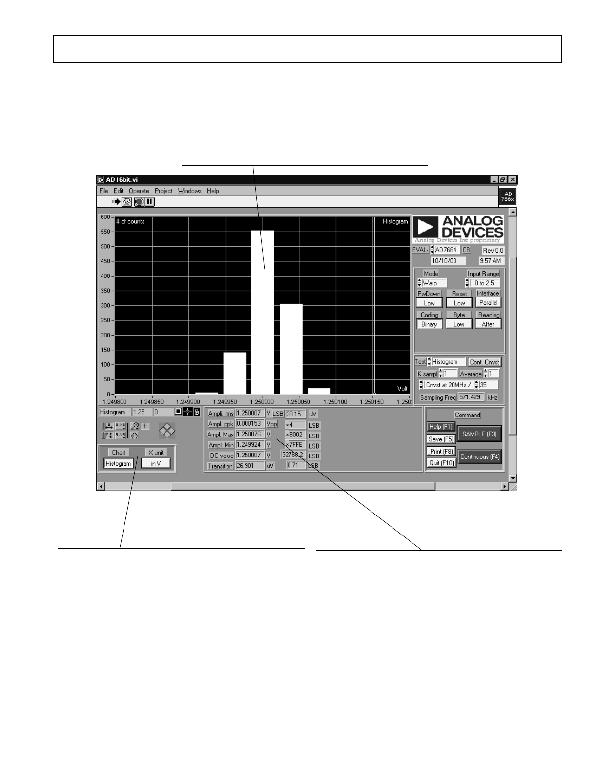
The results are displayed on this chart. You may also use the
cursor (yellow) and drag it to your desired location, where the
X-axis value and the Y-axis value will be displayed.
This control allows you the choice of display. You have the
option of Time or Histogram. You also have the option of
changing the X-axis unit
REV PrK
Figure 9. Histogram Screen
Different measurements are displayed here. The DC value,
transition noise, and other values.
–13–
PRELIMINARY TECHNICAL DATA
EVAL-AD766XCB/AD767XCB
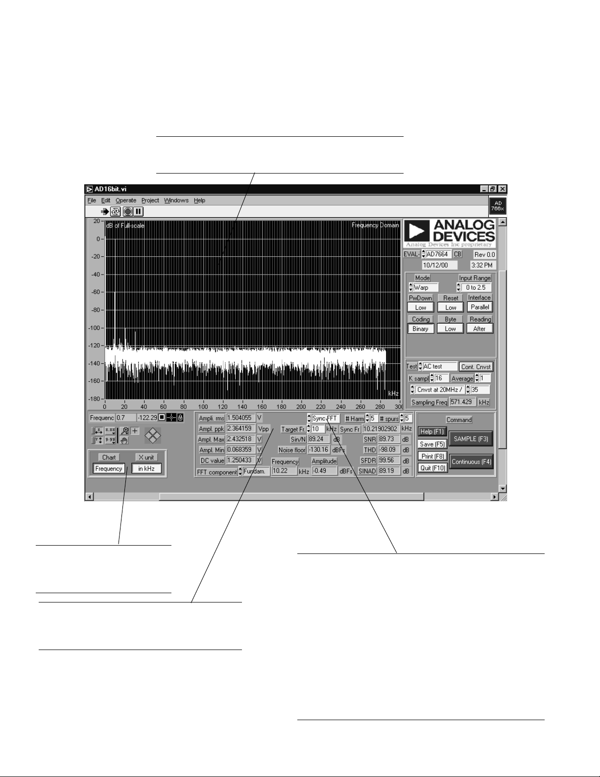
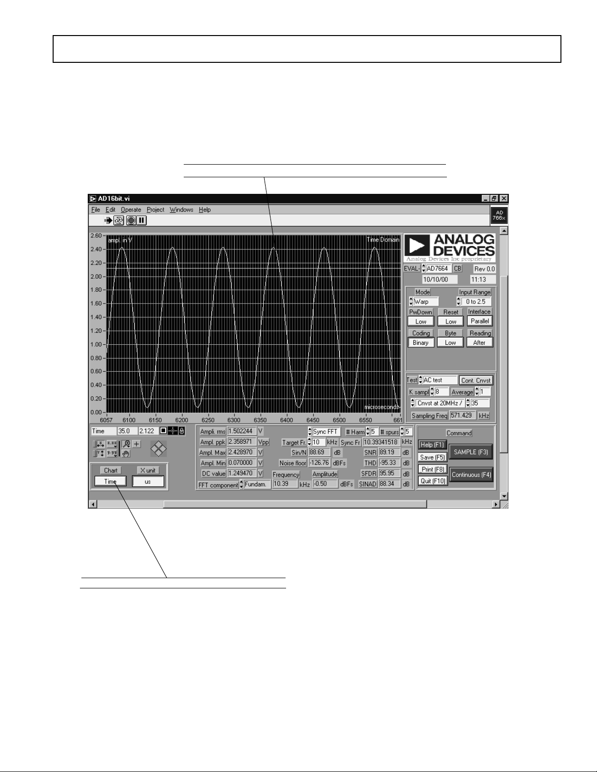
The results are displayed on this chart. You may also use the
cursor (yellow) and drag it to your desired location, where the
X-axis value and the Y-axis value will be displayed.
This is the control that allows you
the choice of either time domain
or frequency domain. You may
also change the X-axis unit here.
AC test results are shown here. You also have the
choice of viewing the amplitude of a certain FFT
component by changing the FFT component
menu.
Figure 10. FFT Screen
You may choose either a Kaiser window or a Blackmann-Harris window or a Sync FFT from this menu. . When choosing a
Sync FFT, you will need to synchronize your analog source to
the sampling frequency. The input frequency should be the
value Sync Fr, which is to the right of Target frequency. The
process for this is as follows:
1. You Choose a Target frequency
2. The software calculates an integer n based on the target
frequency you entered and the sampling frequency, Fsamp.
3. The software rounds up the value n to the next prime
number.
4. The software then calculates the corresponding input frequency (Fin) and displays that as Sync Fr.
The equation, (capture window size) is shown below:
(1/Fsamp) * (number of samples) = n * (1/Fin)
–14–
REV. PrK
PRELIMINARY TECHNICAL DATA
EVAL-AD766XCB/AD767XCB
You can also view the output in the Time domain as shown below.
Figure 11. Time-Domain Screen
To view the Time domain, select Time in this menu.
REV PrK
–15–
 Loading...