

查询EVAL-AD7476供应商查询EVAL-AD7476供应商
a
Evaluation Board for 1MSPS,
12-/ 10-Bit ADCs
EVAL-AD7476/77CB
FEATURES
Full-Featured Evaluation Board for the AD7476/
AD7477
EVAL-CONTROL BOARD Compatible
Stand Alone Capability
On-Board Analog Buffering and Reference
Various Linking Options
PC Software for Control and Data Analysis when used
with EVAL-CONTROL BOARD
INTRODUCTION
This Technical Note describes the evaluation board for
the AD7476/77. The AD7476/77 are, respectively, 12 bit
and 10 bit, high speed, low power, successive-approximation ADC's. The parts operate from a single 2.35 V to
5.25 V power supply and feature throughtput rates up to
1MSPS. The parts contain a low-noise, wide bandwidth
track/hold amplifier which can handle input frequencies in
excess of 1MHz. Full data on the AD7476/77 is available
in the AD7476/77 data sheet available from Analog Devices and should be consulted in conjunction with this
Technical Note when using the Evaluation Board.
On-board components include an AD780 which is a pin
programmable +2.5 V or +3 V ultra high precision
bandgap reference, an OP467 quad op-amp used to buffer
the analog inputs and the REF195 precision bandgap,
voltage reference, providing a 5 V reference voltage.
There are various link options which are explained in
detail on page 2.
Interfacing to this board is through a 96-way connector.
This 96-way connector is compatible with the EVALCONTROL BOARD which is also available from Analog
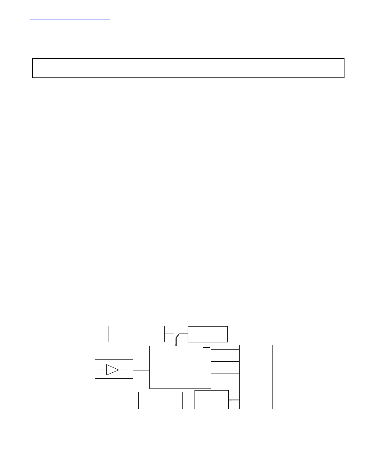
Figure 1. FUNCTIONAL BLOCK DIAGRAM
Devices. External sockets are provided for the AIN input,
the VIN input and the VBIASED input.
OPERATING THE AD7476/77 EVALUATION BOARD
Power Supplies
When using this evaluation board with the EVAL-CONTROL BOARD all supplies are provided from the EVALCONTROL BOARD through the 96 way connector.
When using the board as a stand alone unit external supplies must be provided. This evaluation board has seven
power supply inputs: AV
DV
DD
and D
. +5 V must be connected to the AV
GND
DD
, A
, +12 V, -12 V, A
GND
GND
DD
,
input to supply the AD780 and the Ref195 voltage reference. The V
for the AD7476/77 can be supplied from
DD
either the AVDD external supply or from the selected
voltage reference chip. +12 V and -12 V are used to supply the OP467 quad op-amp. 0V is connected to one or
both of the A
supply a separate +5V for the 74LS04 DV
D
input must be tied to 0V. The supplies are de-
GND
inputs. The DVDD input can be used to
GND
pin. The
DD
coupled to the relevant ground plane with 10µF tantalum
and 0.1µF multilayer ceramic capacitors at the point
where they enter the board. The supply pins of the quad
op-amp and references are also decoupled to A
GND
with
10µF tantalum and a 0.1µF ceramic capacitors. The
AD7476/77 AV
supply pin is decoupled to A
DD
GND
with
10uF tantalum and 0.1µF multilayer ceramic capacitors.
Extensive ground planes are used on this board to minimize the effect of high frequency noise interference. There
are two ground planes, A
GND
and D
. These are con-
GND
nected at one location close to the AD7476/77.
External
Power Supplies
Vdd
Input Buffer
AD7476/77
ADC
VIN
Bias-up
Circuit
REV. 0
Information furnished by Analog Devices is believed to be accurate and
reliable. However, no responsibility is assumed by Analog Devices for its
use, nor for any infringements of patents or other rights of third parties
which may result from its use. No license is granted by implication or
otherwise under any patent or patent rights of Analog Devices.
Voltage
Reference
CS
SCLK
SDATA
Power
Supply
Circuit
One Technology Way, P.O. Box 9106, Norwood. MA 02062-9106, U.S.A.
Tel: 617/329-4700 Fax: 617/326-8703
96 Pin
DIN
Connector

EV AL-AD7476/77CB
LINK AND SWITCH OPTIONS
There are 12 link options which must be set for the required operating setup before using the evaluation board. The
functions of these options are outlined below.
Link No. Function.
LK1 This link option is used to select a 50W termination on the analog input buffer circuit.
When this link is “inserted” the 50W termination is applied.
When this link is “removed” the 50W termination is removed.
LK2 This link option controls the program pin of the AD780 voltage reference.
When this link is “inserted” the AD780 output voltage is set to +3.0 V.
When this link is “removed” the AD780 output voltage is set to +2.5 V.
LK3 This link is used to select a 50W termination on the input of the bias-up circuit.
When this link is “inserted” the 50W termination is applied.
When this link is “removed” the 50W termination is removed.
LK4 This link option is used to connect the output of either the REF195 or the AD780 to the V
AD7476/77 ( if link 12 is in position C).
When this link is in position A the AD780 supplies the V
When this link is in position B the REF195 supplies the V
voltage for the AD7476/77.
DD
voltage for the AD7476/77.
DD
LK5 This link option sets the DC bias voltage that is applied to the optional bias-up/filter circuit.
When this link is in position “A”, the bias voltage is set to the same level as the voltage that is applied
to the AD7476/77 V
pin. In this configuration a bipolar analog input applied to the Vin SMB socket is
DD
biased up by the bias circuit and is presented at the Vbiased SMB as a uni-polar signal biased around
V
/2.
DD
When this link option is placed in position “B”, the bias voltage is set to A
. In this configuration the bias-
GND
up circuit is not used.
LK6 This link option is used to select the source of the +12 V supply.
In position A, the +12 V is supplied from the EVAL-CONTROL BOARD through the 96 way connector.
In position B, the +12 V is supplied from an external source through the power connector, J6.
LK7 This link option is used to select the source of the -12 V supply.
In position A, the -12 V is supplied from the EVAL-CONTROL BOARD through the 96 way connector.
In position B, the -12 V is supplied from an external source through the power connector, J6.
LK8-9 These links control the transfer of data from the AD7476/77 during a conversion for various frequencies of
SCLK.
Link 8 and 9 should be in position "A" for slower SCLK frequencies, giving valid data on the rising edge.
Link 8 and 9 should be in position "B" for fast SCLK frequencies, giving valid data on the following edge.
LK10 This link selects the source of the Vcc +5 V supply for the 74LS04.
When this link is in position "A", Vcc power is supplied from the same power source supplying the AD7476/
77 V
pin.
DD
When this link is in position "B", V
power must be must be supplied from an external source via the power
CC
connector, J5.
LK11 This link option is used to connect the input of the VIN analog buffer to the AIN input socket or to A
When this link is in position “A” the AIN socket is tied to the input of the VIN buffer. In this configuration,
an analog signal applied to the Ain input socket is buffered and presented at the AD7476/77 VIN input.
When this link is in position “B” the VIN buffer input is tied to A
LK12 This link selects the source of the V
DD
When this link is in position “A” the V
When this link is in position “B” the V
When this link is in position “C” the V
supplied to the AD7476/77.
must be supplied from an external source via J5.
DD
is supplied from the EVAL-CONTROL BOARD.
DD
is supplied from either the AD780 or the REF195 references.
DD
GND
.
pin of the
DD
GND
.
–2–
REV. 0

EV AL-AD7476/77CB
SET-UP CONDITIONS
Care should be taken before applying power and signals to the evaluation board to ensure that all link positions are
as per the required operating mode. Table I shows the position in which all the links are set when the evaluation
board is sent out.
Table I. Initial Link and Switch Positions
Link No. Position Function.
LK1 Removed 50W termination resistor is not applied to the input of the VIN circuit.
LK2 Removed AD780 is set to provide a +2.5V reference.
LK3 Removed 50W termination resistor is not applied to the input of the bias-up circuit.
LK4 Removed This is not relevant due to the position of LK12.
LK5 A EVAL-CONTROL BOARD is selected as the DC bias voltage for the optional
bias-up/filter circuit.
LK6 A +12V supplied from EVAL-CONTROL BOARD via J4.
LK7 A -12V supplied from EVAL-CONTROL BOARD via J4.
LK8 B SCLK signal from EVAL-CONTROL BOARD is not inverted, (for faster values
of SCLK).
LK9 B SCLK signal from EVAL-CONTROL BOARD is not inverted, (for faster values
of SCLK).
LK10 Removed This is not relevant due to the position of LK8 and LK9, (As 74LS04 is not in
use).
LK11 A Ain SMB is connected to the input of the analog input buffer.
LK12 B VDD for the AD7476/77 is supplied from the EVAL-CONTROL BOARD via J4.
REV. 0
–3–
EV AL-AD7476/77CB
EVALUATION BOARD INTERFACING
Interfacing to the evaluation board is via a 96-way connector, J4. J4 is used to connect the evaluation board to the
EVAL-CONTROL BOARD or other system. The pinout
for the J4 connector is shown in Figure 2 and its pin designations are given in Table II.
1
A
B
C
1
32
32
Figure 2. Pin Configuration for the 96-Way
Connector, J1
96-Way Connector Pin Description
D R0 Data Receive Zero. This input is connected to the
SDATA pin of the AD7476/77.
TFS0/RFS0 Transmit/Receive Frame Sync Zero. These two
outputs are connected to the CS pin of the
AD7476/77.
SCLK0 Serial Clock Zero. This serial clock is connected
to the SCLK pin of the AD7476/77 with the
option of an inverting buffer.
DGND Digital Ground. These lines are connected to
the digital ground plane on the evaluation
board. It allows the user to provide the digital
supply via the connector along with the other
digital signals.
AGND Analog Ground. These lines are connected to
the analog ground plane on the evaluation board.
AV
DD
Analog +5 V Supply. These lines are connected
to the AV
supply line on the board.
DD
+12V +12 V Supply. This line is connected to the +12
V supply line on the board via LK6.
-12V -12 V Supply. This line is connected to the -12
V supply line on the board via LK7.
Table II. 96-Way Connector Pin Functions.
Row A RowB RowC
1
2
3
4 DGND DGND DGND
5 DR0
6 TFS0 RFS0
7 SCLK0 SCLK0
8
9
10
11
12 DGND DGND DGND
13
14
15
16 DGND DGND DGND
17
18
19
20 DGND DGND DGND
21 AGND AGND AGND
22 AGND AGND AGND
23 AGND AGND AGND
24 AGND AGND AGND
25 AGND AGND AGND
26 AGND AGND AGND
27 AGND
28 AGND
29 AGND AGND AGND
30 -12 V AGND +12 V
31
32 AVDD AVDD AVDD
–4–
Note : The unused pins of the 96-way connector are not shown.
REV. 0

EV AL-AD7476/77CB
SOCKETS
There are three input sockets relevant to the operation of
the AD7476/77 on this evaluation board. The function of
these sockets is outlined in Table III.
Table III. Socket Functions
Socket Function
J1 Sub-Miniature BNC Socket for AIN analog
input.
J2 Sub-Miniature BNC Socket for analog in-
put to bias-up circuit.
J3 Sub-Miniature BNC Socket for analog out-
put from bias-up circuit.
CONNECTORS
There are three connectors on the AD7476/77 evaluation
board as outlined in Table IV.
Table IV. Connector Functions
Connector Function
J4 96-Way Connector used to Interface to
EVAL-CONTROL BOARD.
J5 External VDD & A
J6 External +12 V, -12 V & A
nector.
power connector.
GND
power con-
GND
OPERATING WITH THE EVAL-CONTROL BOARD
The evaluation board can be operated in a stand-alone
mode or operated in conjunction with the EVAL-CONTROL BOARD. This EVAL-CONTROL BOARD is
available from Analog Devices under the order entry
"EVAL-CONTROL BOARD". When operated with this
control board, all supplies and control signals to operate
the AD7476/77 are provided by the EVAL-CONTROL
BOARD when it is run under control of the AD7476/77
software which is provided with the AD7476/77 evaluation
board package. This EVAL-CONTROL BOARD will
also operate with all Analog Devices evaluation boards
which end with the letters CB in their title.
The 96-way connector on the EVAL-AD7476/77CB plugs
directly into the 96-way connector on the EVAL-CONTROL BOARD. No power supplies are required in the
system. The EVAL-CONTROL BOARD generates all
the required supplies for itself and the EVAL-AD7476/
77CB. The EVAL-CONTROL BOARD is powered from
a 12 V ac transformer. This is a standard 12 V ac transformer capable of supplying 1A current and is available as
an accessory from Analog Devices under the following
part numbers:
EVAL-110 VAC-US: For use in the U.S. or Japan
EVAL-220 VAC-UK: For use in the U.K.
EVAL-220 VAC-EU: For use in Europe
These transformers are also available for other suppliers
including Digikey (U.S.) and Campbell Collins (U.K.).
Connection between the EVAL-CONTROL BOARD and
the serial port of a PC is via a standard RS-232 cable
which is provided as part of the EVAL-CONTROL
BOARD package. Please refer to the manual which accompanies the EVAL-CONTROL BOARD for more
details on the EVAL-CONTROL BOARD package.
REV. 0
–5–

EV AL-AD7476/77CB
Figure 3. Main Screen
SOFTWARE DESCRIPTION
Included in the EVAL-AD7476/77CB evaluation board
package is a PC-compatible disk which contains software
for controlling and evaluating the performance of the
AD7476/77 when it is operated with the EVAL-CONTROL BOARD. The EVAL-AD7476/77CB Demonstration/Evaluation Software runs under DOS 4.0 or later and
requires a minimum of a 386-based machine with 400kB
of base RAM and 500kB of free hard disk space. The user
interface on the PC is a dedicated program written especially for the AD7476/77.
The disk which accompanies the EVAL-AD7476/77CB
contains several files. The user should create a new directory on the main PC drive and label this "AD7476/77".
Then, all files on the EVAL-AD7476/77CB disk should
be copied into this directory. The Mouse Driver on the
PC should be enabled before running the software. If this
has not been loaded, the program will not run.
To run the software, simply make the AD7476/77 directory the current directory and type "go". When the evaluation program starts, the user sees the screen shown on
Figure 3 (without any FFT or scope waveforms). This is
the main screen and it is divided into three parts. The top
part provides the main control interface for the AD7476/
77 evaluation software. The middle part of the main
screen functions as a Digital Storage Oscilloscope and the
bottom part of the main screen operates as either a Digital
Spectrum Analyzer or a Histogram analyzer.
Each part of the screen has several buttons that can be
pressed by using the mouse or the keyboard. To press a
button using the mouse, simply use it to move the onscreen pointer to the button to be activated and click. To
use the keyboard, simply press the appropriate key as
highlighted on the button. Lower case letters must be
used. When a button is pressed, it is highlighted on the
screen. The next button can be highlighted by using the
Tab key or the previous button by holding down the shift
key and the Tab key together. The highlighted button can
also be pressed by pressing the space bar. Pressing the
ESC key halts any operation currently in progress. In this
document, if a button can be activated from the keyboard
then the key used is shown in bold in the button name.
For example, "no prog" has the "p" highlighted in bold,
indicating that the button can be activated by pressing the
p key.
Some buttons have a red indicator. A red indicator on the
button means that the function associated with that button
is on. Absence of the red indicator light means that the
function associated with the button is off. The on/off
status of these buttons is changed simply by selecting the
button.
Setting up the EVAL-CONTROL BOARD
When the software is run, the "F2 Setup" button in the top
left of the screen should be selected to pop up the setup
menu (see fig. 4). This menu sets up the EVALCONTROL BOARD for use with the EVAL-AD7476/
77CB.
Firstly, a configuration file must be chosen. The configuration file contains the default configuration information for
the EVAL-CONTROL BOARD, the Digital Spectrum
Analyzer and the Digital Storage Oscilloscope. It also tells
the AD7476/77.EXE software which .HIP file to download
to the ADSP-2111. The .HIP file contains the DSP code
which is executed by the ADSP-2111. Normally, the "no
prog" button is off, so when the configuration file is loaded,
the .HIP file is automatically downloaded to the ADSP-
2111. However, if the "no prog" button is on, then the .HIP
file is not downloaded to the ADSP-2111.
–6–
REV. 0

EV AL-AD7476/77CB
There are two configuration files for the AD7476. (these are
AD7476 and AD7476D) and two for the AD7477 (these are
AD7477 and AD7477D). Each file is particular to a certain
mode of operation for the device. See modes of operation
selection in the AD7476/77 datasheet. The AD7476 file is
the normal mode program for the AD7476. This should
execute when the F3 button is pressed after the AD7476
configuration file has been loaded. When the button is
pressed the conversion result will be output on to the screen
as either an fft plot or as a historgram.
The AD7476 program also offers the user the option of
entering the "power down" mode. This can done by entering
the setup screen (see figure 4) and using the Power down
button. As there will be no valid data from this operation,
there will be no result on screen. To exit the "powerdown"
mode the user must "Power up" the part before preforming
a valid conversion. This can be done by again entering the
setup screen and pressing the "Power up" button. As there is
no valid data from this dummy conversion there is no result
to be output on screen.
The AD7477 program offers the same options as the AD7476
program but it is configured for a 10 bit part (AD7477).
When the AD7476D configuration file is loaded it offers the
user a "power up - convert - powerdown" sequence option.
This program is ideal for use when the device is not being
operated constantly, as it saves on power. The 12 bit result
from the conversion is output on the screen as either an fft
plot or a histogram.
To perform the same sequence (power up - convert powerdown)on the 10 bit AD7477 part, the AD7477D
configuration file should be used.
MAIN SCREEN
Figure 4. Setup Menu Screen
Th
e top left part of the main screen contains eight buttons
which are selected using the mouse or by using the function
keys from the keyboard. These buttons and the actions they
perform are:
F1: Info. This button shows information on the software.
F2: Setup. This button activates the setup menu.
F3: Samp. When this key is pressed, the software causes
the AD7476/77 to perform a number of conversions
as determined by the setup menu (see above). The
data from these conversions is then analyzed by the
AD7476/77 evaluation software. Another set of
samples may be taken by pressing the F3 key again.
F4: Cont. Pressing this button causes the software to
repeatedly perform conversions and analyze them.
Once the conversions and analysis has been done fo
one set of samples, the software automatically repeats
r
the process. It continues to do this until the ESC key
is pressed.
F5: Save. This saves a set of samples to a file for use either
at a later date or with other software. The samples can
be saved either as "volts", "ints" or "binary". The
format of all these files is ASCII text. Note that the
AD7476/77 software can only load files saved in the
"ints" format. Files saved in the "volts" and "ints"
formats can be used with packages such as Mathcad.
Files saved in the "binary" format are for viewing
purposes only.
F6: Load. This allows the user to load data from a file
with a .DAT extension. Only data that was saved as
ints can be loaded and analyzed. A configuration file
must be loaded via the "F2 Setup" menu before the
data file can be analyzed. If there is no EVALCONTROL BOARD connected to the PC, then the
"no prog" button in the "F2 Setup" menu must be on.
Once a configuration file has been loaded, the data
loaded from the .DAT file is analyzed according to
the settings in the "F2 Setup" menu.
F7: Reset. Choosing this option resets the EVAL-CON-
TROL BOARD.
F10: Quit. This quits the AD7476/77 evaluation software
and returns control to the operating system.
INFORMATION WINDOWS
There are three information windows at the top of the main
screen. The left-hand window is the configuration window
and gives details about part being evaluated. It shows the
name of the program that has been downloaded to the EVALCONTROL BOARD, the sampling frequency, the number
of bits, the analog input range of the part and the output code
format of the part. The right-hand large window is the Status
window. This window provides feedback to the user as to
what operations are currently being performed by the software and also displays error messages. Directly underneath
the status window is a small window that shows the selected
conversion sequence and the maximum and minimum values
of the most recently captured samples for all channels in the
conversion sequence.
Test Mode
At the top right of the main screen are the Test Mode buttons.
These buttons determine what sort of testing is done on the
samples captured by the software. Both an ac analysis and dc
analysis can be performed. The function of these buttons are:
fft plot Choosing this button causes the Digital Spectrum
Analyzer to appear at the bottom of the screen.
Histogram: Choosing this button causes the Histogram
Analyzer to be displayed at the bottom of the screen.
There is one other button near the top of the screen, beside
the "F10 Quit" button. This is:
blackman-harris: When performing a Fourier transform
of the sampled data, this button determines whether or not the
data is windowed by a blackman-harris window before the
transform. When this button is on, the data is windowed.
When this button is off, the data isn't windowed. See the
Digital Spectrum Analyzer section for more details.
REV. 0
–7–

EV AL-AD7476/77CB
DIGITAL STORAGE OSCILLOSCOPE.
When samples of data are captured, they are displayed on the
Digital Storage Oscilloscope. If the blackman-harris button
is turned on then the windowed data is also displayed on the
oscilloscope. The 'scope has been designed to act in a similar
way as a conventional oscilloscope. To the right of the
oscilloscope are several buttons that control the manner in
which data is displayed on the 'scope. The timebase for the
oscilloscope is automatically chosen by the software if the
Time/Div "Auto" button is on. The user can also select the
timebase by clicking in the Time/Div window and scrolling
up and down through the possible timebases. Similarly, the
vertical scale of the oscilloscope is chosen automatically if the
Volt/Div "Auto" button is on. The user also has the option
of selecting the desired vertical scale in a similar manner to
selecting the timebase.
The other buttons associated with the oscilloscope are:
grid This button toggles the grid display of the oscil-
loscope on and off.
axis This button toggles the axis display of the oscil-
loscope on and off
text This button toggles the text displayed on the
oscilloscope screen on and off.
li ne When the line button is on, the displayed samples
are joined together by lines. When this button is
off, the samples are displayed as points.
ac When this button is on, the dc component of the
sampled signal is removed and the signal is
displayed. This has the effect of centering the
signal vertically on the oscilloscope screen. When
this button is off, the dc component is not
removed and the signal is displayed with its
horizontal axis corresponding to a code of 0. The
ac display option is useful for zooming in on a
low-level signal that has a large dc offset.
dual When the "dual" button is on, the oscilloscope
screen is divided into two parts with the sampled
data display centered on one horizontal axis and
the windowed data display centered on another.
When the "dual" button is off, both traces are
centered on the same horizontal axis.
1 This button toggles the sampled data trace on and
off.
2 This button toggles the windowed data trace on
and off.
HISTOGRAM ANALYZER
The histogram analyzer counts the number of occurrences of
each code in the captured samples and displays a histogram
of these counts. The most frequently occurring code is
displayed in the center of the histogram. The analyzer is
normally used with a dc input signal and calculates the mean
and the standard deviation of the sampled data. The mean
and standard deviation are displayed in both volts and in units
of the lsb size of the converter. The histogram gives a good
indication of the dc noise performance of the ADC. The
standard deviation shows directly the noise introduced in the
conversion process.
Figure 5 Histogram Screen
–8–
REV. 0

EV AL-AD7476/77CB
REV. 0
Figure 6. AD7476/77 Evaluation Board Circuit Diagram
–9–

EV AL-AD7476/77CB
Table V. AD7476/77 Evaluation Board Bill Of Materials
Qty. Reference Designator Description/Value Manuf. No. Supplier No.
1 U1 AD7476ART/AD7477ART ADI AD7476ART/77ART ADI
1 U2 AD711KN ADI AD711KN ADI
1 U3 ADOP467G ADI ADOP467G ADI
1 U4 74LS04 DM74LS04N FEC 373-450
1 U5 ADREF195G ADREF195GP ADI
1 U6 AD780AN ADI AD780AN ADI
5 R1 - R4 R6 1K 0.25W 0.1% RC55 Welwyn FEC 339-179
1 R5 3K 0.25W 0.1% RC55 Welwyn FEC 339-635
2 R7 R8 51W 0.25W 1% Multicomp FEC 543-070
1 C10 0.1uF Ceramic 1206 Case 12065C104KATDA FEC 895-210
1 C9 10uF 20 V TAJ-C Case TAJC106K020X FEC 498-798
2 C11 C12 68pF Ceramic MR051A680JT0001 FEC 669-714
1 C33 0.01uF Ceramic 50 V MCDR25103X7RK0050 FEC 750-890
14 C2 C3 C5 C8 C13 C14 C16 0.1uF Ceramic 50 V MCDR25104X7RK0050 FEC 750-920
C18 C20 C23 C25 C26 C29 C31
15 C1 C4 C6 C7 C9 C15 C17 10uF 35 V Tant. TAP10K35CCSY FEC 664-881
C19 C21 C22 C24 C27 C28 C30 C32
3 J1 J2 J3 50W Gold Plated SMB MA-com FEC 310-682
1 J4 DIN41612 C96 900 plug Harting 0903-196-7921 FEC 104-986
1 J5 2 Pin Power Connector Lumberg KRM2 FEC 151-785
1 J6 3 PIN Power Connector Lumberg KRM3 FEC 151-786
3 LK1 LK2 LK3 2 Way Jumper Harwin FEC 511-705
8 LK4 - LK11 2x2 Way Jumper Harwin FEC 511-780
1 LK12 2x3 Way Jumper Harwin FEC 511-780
12 LK1 - LK12 Shorting links Harwin
4 T1 T2 T3 T4 White Testpoint Keystone Cat. No. 5002 Futura Elect.
5 U2 U3 U4 U5 U6 Ultra low profile socket pins Harwin FEC 519-959
4 Each Corner Rubber Stick on feet 3M FEC 148-922
1 EVAL-AD7476CB P.C.B.
–10–
FEC
150-410
REV. 0

EV AL-AD7476/77CB
Figure 7. Component Side Artwork
REV. 0
Figure 8. Solder Side Artwork
–11–

EV AL-AD7476/77CB
Figure 9. AD7476/77 Component Placement Drawing.
–12–
REV. 0
 Loading...