a
PLL/Multibit - DAC
AD1958
FEATURES
5 V Stereo Audio DAC System
Accepts 16-/18-/20-/24-Bit Data
Supports 24 Bits, 192 kHz Sample Rate
Accepts a Wide Range of Sample Rates Including:
32 kHz, 44.1 kHz, 48 kHz, 88.2 kHz, 96 kHz, and 192 kHz
Multibit Sigma-Delta Modulator with “Perfect Differential
Linearity Restoration” for Reduced Idle Tones and
Noise Floor
Data Directed Scrambling DAC—Least Sensitive to Jitter
Single-Ended Output for Easy Use
108 dB Signal-to-Noise (Not Muted) at 48 kHz Sample
Rate (A-Weighted Stereo)
109 dB Dynamic Range (Not Muted) at 48 kHz Sample
Rate (A-Weighted Stereo)
–96 dB THD + N (Stereo)
75 dB Stop Band Attenuation
On-Chip Clickless Volume Control
Hardware and Software Controllable Clickless Mute
Serial (SPI) Control for: Serial Mode, Number of Bits,
Sample Rate, Volume, Mute, De-Emphasis
Digital De-Emphasis Processing for 32 kHz, 44.1 kHz,
and 48 kHz Sample Rates
Programmable Dual Fractional-N PLL Clock Generator
27 MHz Master Clock Oscillator
Better than 100 ps rms Master Clock Jitter
Generated System Clocks
SCLK0: 33.8688 MHz
SCLK1: 22.5792 MHz, 24.576 MHz, 33.8688 MHz, or
36.864 MHz
SCLK2: 16.9344 MHz
Flexible Serial Data Port with Right-Justified, Left-
Justified, I
2
S-Compatible, and DSP Serial Port Modes
28-Lead SSOP Plastic Package
APPLICATIONS
DVD, CD, Home Theater Systems, Automotive Audio
Systems, Sampling Musical Keyboards, Digital Mixing
Consoles, Digital Audio Effects Processors
PRODUCT OVERVIEW
The AD1958 is a complete high-performance single-chip stereo
digital audio playback system. It is comprised of a multibit sigmadelta modulator, digital interpolation filters, and analog output
drive circuitry with an on-board dual PLL clock generator.
Other features include an on-chip stereo attenuator and mute,
programmed through an SPI-compatible serial control port.
The AD1958 is fully compatible with all known DVD formats
including 96 kHz and 192 kHz sample frequencies and 24 bits.
It also is backwards-compatible by supporting 50 µs/15 µs
digital de-emphasis for “redbook” compact discs, as well as
de-emphasis at 32 kHz and 48 kHz sample rates.
The AD1958 has a simple but flexible serial data input port that
allows for glueless interconnection to a variety of ADCs, DSP
chips, AES/EBU receivers, and sample rate converters. The
AD1958 can be configured in left-justified, I
2
S, right-justified,
or DSP serial-port-compatible modes. It can support 16, 20,
and 24 bits in all modes. The AD1958 accepts serial audio data
in MSB first, two’s-complement format, and operates from a
single 5 V power supply. It is fabricated on a single monolithic
integrated circuit and housed in a 28-lead SSOP package for
operation over the temperature range –40°C to +105°C.
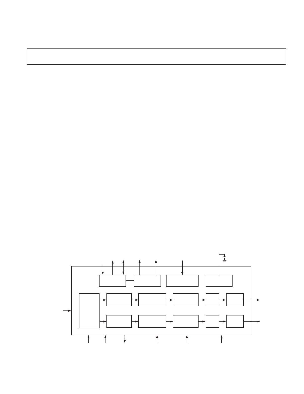
FUNCTIONAL BLOCK DIAGRAM
MCLK
XOUT
OSC
ATTEN/MUTE
ATTEN/MUTE
PLL
CIRCUIT
INTERPOLATOR
INTERPOLATOR
16-/20-/24BIT DIGITAL
DATA INPUT
XIN
AD1958
SERIAL
DATA
INTERFACE
3
RESET MUTE ZERO FLAG PLL SUPPLY DIGITAL SUPPLY ANALOG SUPPLY
LOOP
FILTERS
REV. 0
Information furnished by Analog Devices is believed to be accurate and
reliable. However, no responsibility is assumed by Analog Devices for its
use, nor for any infringements of patents or other rights of third parties that
may result from its use. No license is granted by implication or otherwise
under any patent or patent rights of Analog Devices.
CLOCK
OUTPUTS
8
f
S
8
f
S
CONTROL DATA
INPUT
323
SERIAL CONTROL
INTERFACE
MULTIBIT
SIGMA-DELTA
MODULATOR
MULTIBIT
SIGMA-DELTA
MODULATOR
One Technology Way, P.O. Box 9106, Norwood, MA 02062-9106, U.S.A.
Tel: 781/329-4700 www.analog.com
Fax: 781/326-8703 © Analog Devices, Inc., 2001
VO LTAG E
REFERENCE
DAC
DAC
OUTPUT
BUFFER
OUTPUT
BUFFER
322
ANALOG
OUTPUTS
L
R

AD1958–SPECIFICATIONS
TEST CONDITIONS UNLESS OTHERWISE NOTED
Supply Voltages
(AVDD, DVDD, PVDD) 5.0 V
Ambient Temperature 25°C
Input Clock 12.288 MHz (256 × f
Input Signal 996.0938 Hz,
0 dB Full Scale
Input Sample Rate 48 kHz
Measurement Bandwidth 20 Hz to 20 kHz
Word Width 24 Bits
Load Capacitance 100 pF
Load Impedance 47 kΩ
Input Voltage HI 2.0 V
Input Voltage LO 0.8 V
ANALOG PERFORMANCE
Resolution 24 Bits
Signal-to-Noise Ratio (20 Hz to 20 kHz)
No Filter (Stereo) 105 dB
With A-Weighted Filter (Stereo) 108 dB
Dynamic Range (20 Hz to 20 kHz, –60 dB Input)
No Filter (Stereo) 105 dB
With A-Weighted Filter (Stereo) 102 109 dB
Total Harmonic Distortion + Noise (Stereo) –90 –96 dB
PLL Performance
Master Clock Input Frequency 27 MHz
Generated System Clocks
SCLK0 33.8688 MHz
SCLK1 12.288 MHz
SCLK2 22.5792 MHz
Jitter (SCLK0 and SCLK1) 110 175 ps rms
Jitter (MCLK) 60 100 ps rms
Duty Cycle (SCLK0, SCLK1)
1
Duty Cycle (MCLK) 49 50 51 %
Analog Outputs
Single-Ended Output Range (±Full Scale) 3.17 V p-p
Output Capacitance at Each Output Pin 2 pF
Out-of-Band Energy (0.5 × f
(FILTR) 2.39 V
V
REF
to 100 kHz) –90 dB
S
DC Accuracy
Gain Error –5 ± 2.0 +5 %
Interchannel Gain Mismatch –0.15 ± 0.015 +0.15 dB
Gain Drift 150 250 ppm/°C
DC Offset –25 –3 +20 mV
Interchannel Crosstalk (EIAJ Method) –120 dB
Interchannel Phase Deviation ± 0.1 Degrees
Mute Attenuation –100 dB
De-Emphasis Gain Error ± 0.1 dB
NOTES
1
In some combinations with Clock Configuration Mode = 1 (see Table III), SCLK will not be 50%.
2
Performance of right and left channels is identical (exclusive of the Interchannel Gain Mismatch and Interchannel Phase Deviation specifications).
Specifications subject to change without notice.
DIGITAL I/O (–40°C to +105°C )
Input Voltage HI (VIH) 2.0 V
Input Voltage LO (V
Input Leakage (I
Input Leakage (I
High Level Output Voltage (V
Low Level Output Voltage (V
) 0.8 V
IL
@ VIH = 2.4 V) 10 µA
IH
@ VIL = 0.8 V) 10 µA
IL
) IOH = 1 mA 3.5 V
OH
) IOL = 1 mA 0.4 V
OL
Input Capacitance 20 pF
Specifications subject to change without notice.
Mode)
S
Min Typ Max Unit
50 %
Min Typ Max Unit
–2–
REV. 0

AD1958
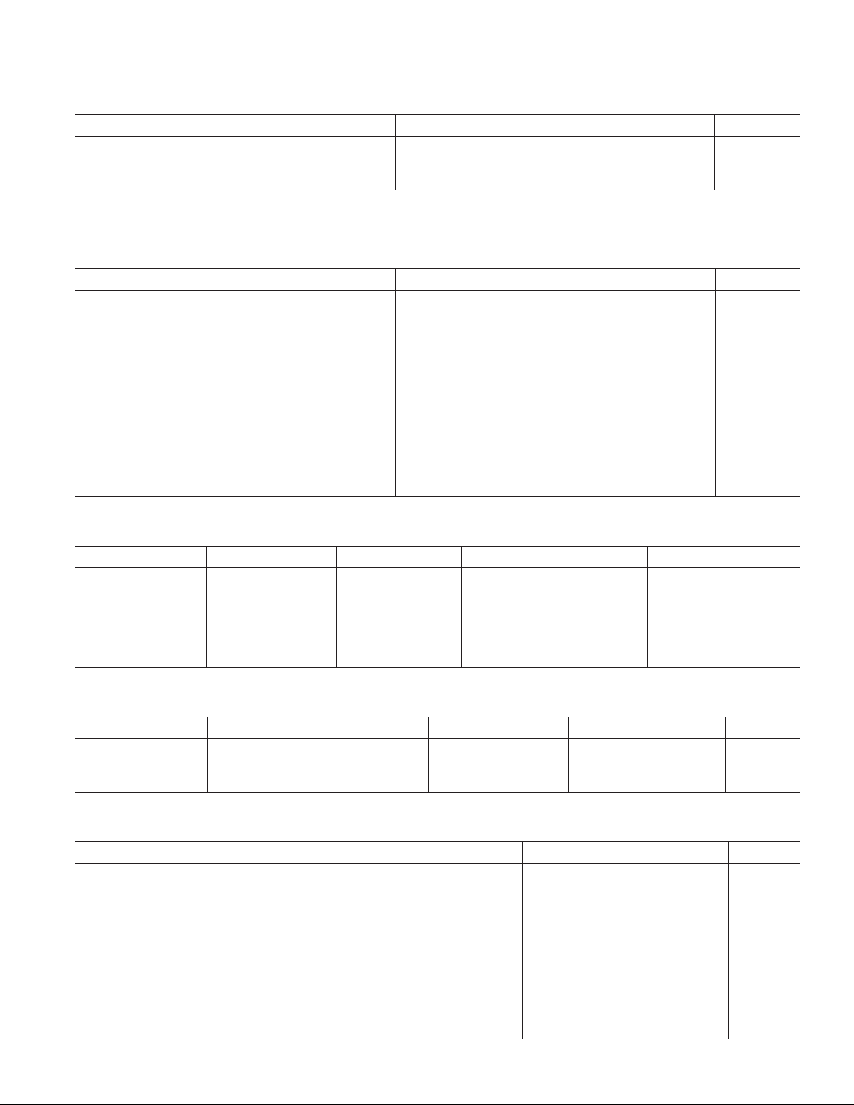
TEMPERATURE RANGE
Min Typ Max Unit
Specifications Guaranteed 25 °C
Functionality Guaranteed –40 +105* °C
Storage –55 +125 °C
NOTE
*105°C ambient guaranteed for a 4-layer board, two 1 oz. planes, two 2 oz. signal layers. Derate to 85 °C for 2-layer board, 2 oz. layers.
Specifications subject to change without notice.
POWER
Min Typ Max Unit
Supplies
Voltage, Analog Digital PLL 4.50 5 5.50 V
Analog Current 36 41 mA
Digital Current 25 29 mA
PLL Current 30 34 mA
Dissipation
Operation—All Supplies 455 540 mW
Operation—Analog Supply 180 mW
Operation—Digital Supply 125 mW
Operation—PLL Supply 150 mW
Power Supply Rejection Ratio
1 kHz 300 mV p-p Signal at Analog Supply Pins –60 dB
20 kHz 300 mV p-p Signal at Analog Supply Pins –50 dB
Specifications subject to change without notice.
DIGITAL FILTER CHARACTERISTICS
Sample Rate (kHz) Pass Band (kHz) Stop Band (kHz) Stop Band Attenuation (dB) Pass Band Ripple (dB)
44.1 DC–20 24.1–328.7 75 ± 0.0002
48 DC–21.8 26.23–358.28 75 ± 0.0002
96 DC–39.95 56.9–327.65 75 ± 0.0005
192 DC–87.2 117–327.65 60 0/–0.04 (DC–21.8 kHz)
0/–0.5 (DC–65.4 kHz)
0/–1.5 (DC–87.2 kHz)
Specifications subject to change without notice.
GROUP DELAY
Chip Mode Group Delay Calculation f
INT8× Mode 24.625/f
INT4× Mode 15.75/f
INT2× Mode 14/f
Specifications subject to change without notice.
S
S
S
S
48 kHz 513 µs
96 kHz 164 µs
192 kHz 72.91 µs
Group Delay Unit
DIGITAL TIMING (Guaranteed over –40°C to +105C, AVDD = DVDD = PVDD = 5.0 V 10%)
Min Unit
t
DMP
t
DML
t
DMH
t
DBH
t
DBL
t
DBP
t
DLS
t
DLH
t
DDS
t
DDH
t
RSTL
Specifications subject to change without notice.
REV. 0
MCLK Period (FMCLK = 256 × FLRCLK) 54 ns
MCLK LO Pulsewidth (All Modes) 15 ns
MCLK HI Pulsewidth (All Modes) 10 ns
BCLK HI Pulsewidth 20 ns
BCLK LO Pulsewidth 20 ns
BCLK Period 60 ns
LRCLK Setup 20 ns
LRCLK Hold (DSP Serial Port Mode Only) 20 ns
SDATA Setup 15 ns
SDATA Hold 15 ns
RST LO Pulsewidth 15 ns
–3–
 Loading...